Digi 50M1663 WLAN Module User Manual cc9m 2443
Digi International Inc WLAN Module cc9m 2443
UserManual.wiki
>
Digi
>
50M1663 User Manual
Hardware Reference Manual
Navigation menu
Upload a User Manual
Namespaces
Wiki Guide
HTML
PDF
Info
Views
User Manual
Discussion / Help
Navigation


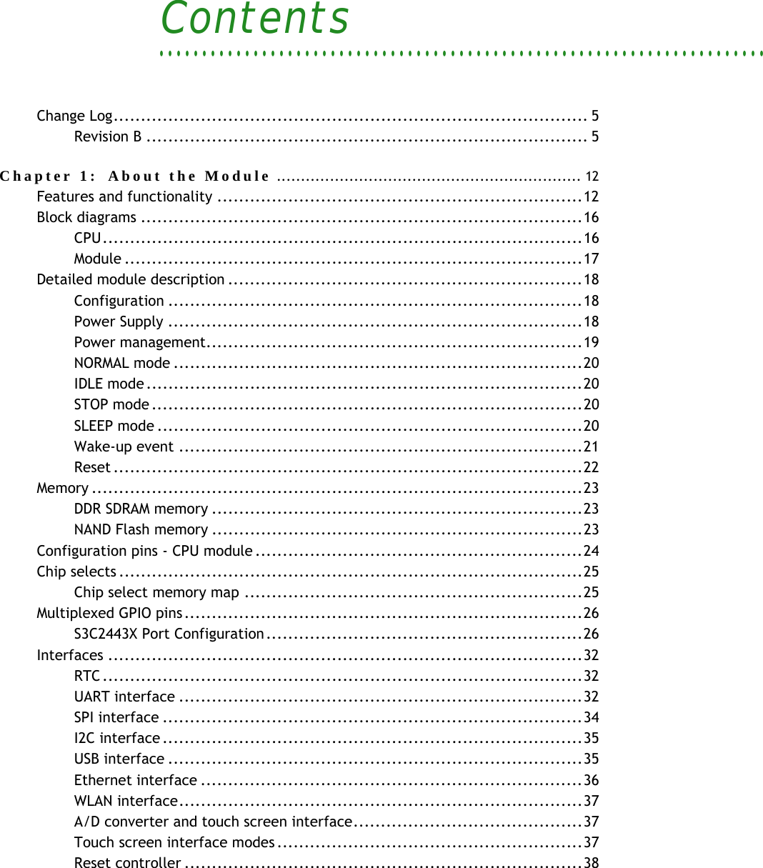
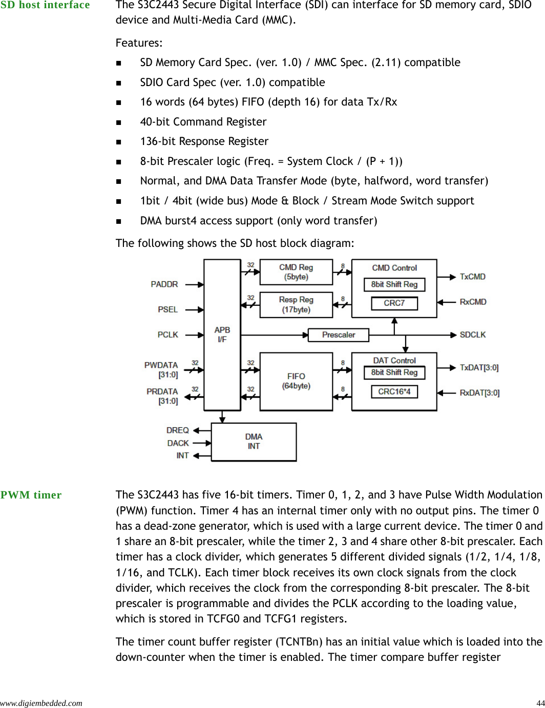
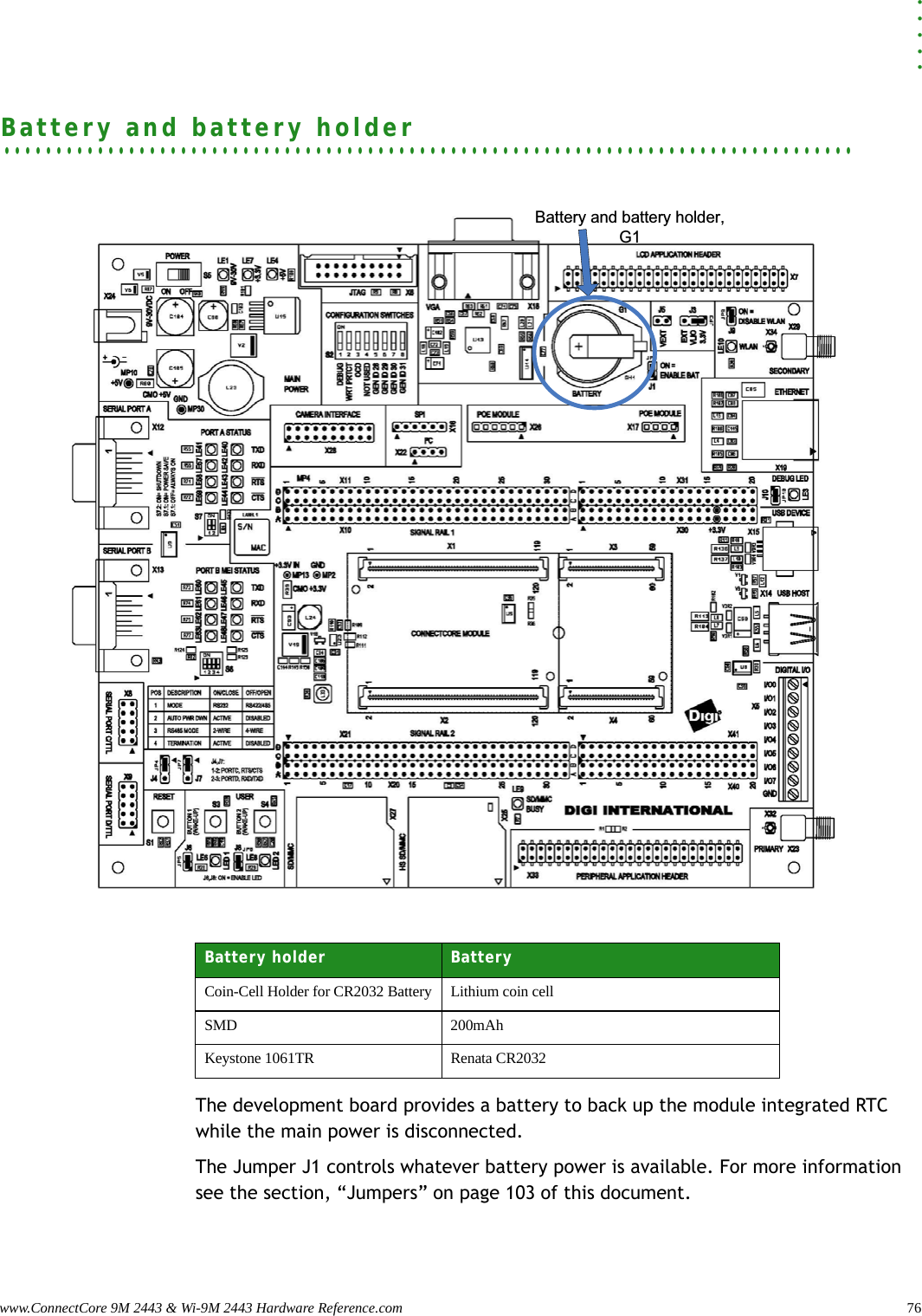
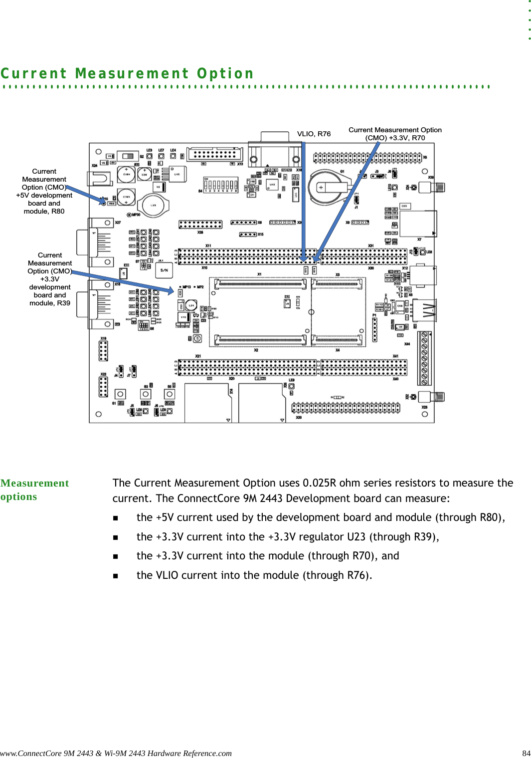
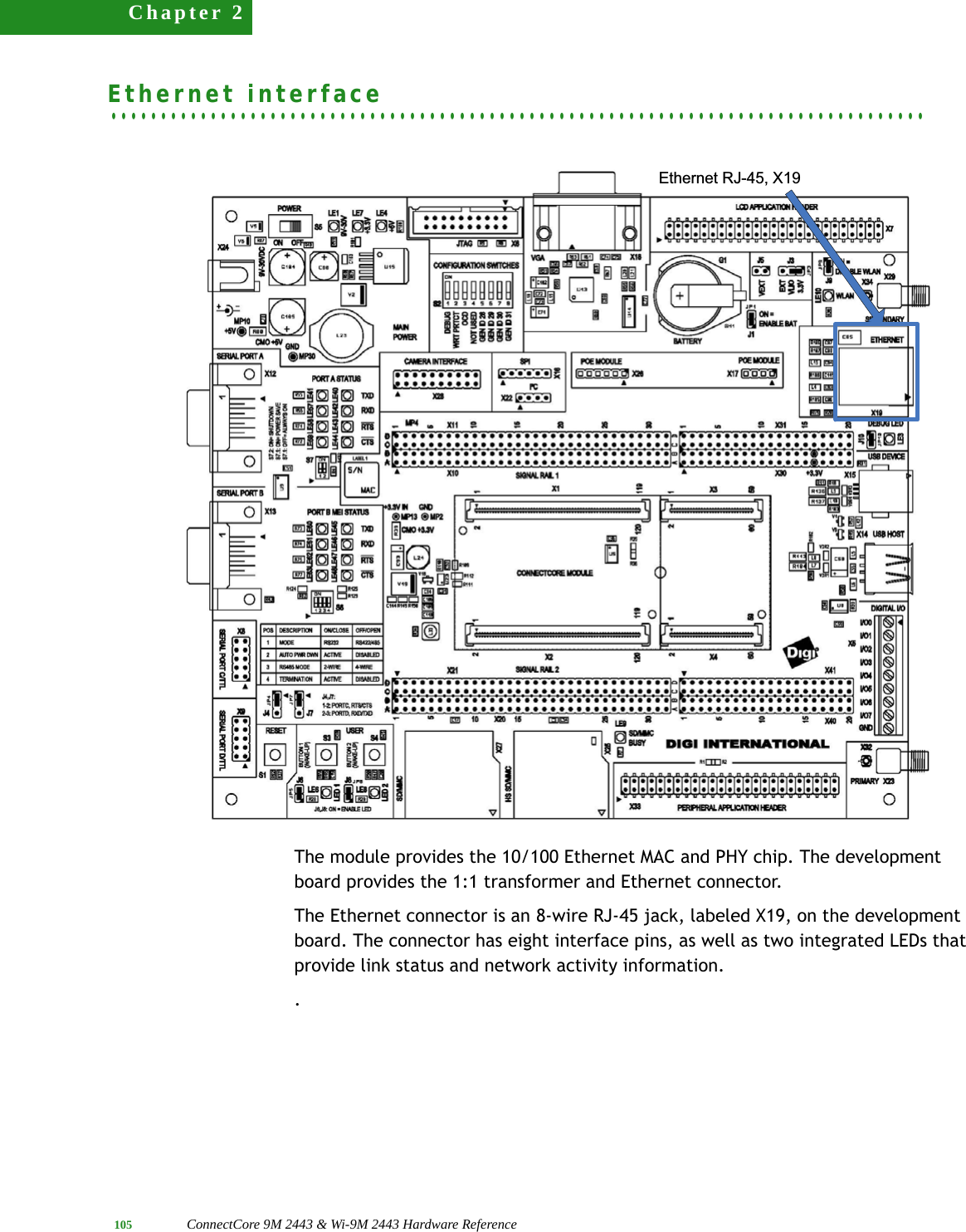
![www.digiembedded.com 18. . . . . . . . . . . . . . . . . . . . . . . . . . . . . . . . . . . . . . . . . . . . . . . . . . . . . . . . . . . . . . . . . . . . . . . . . . . . . . . . . .Detailed module descriptionConfiguration The ConnectCore 9M 2443 Module supports 8 configuration pins:4 pins provided for software configuration, which are routed to standard pin locations on the development board (CONF[7:4]).4 pins provided for hardware configuration, routed to the base board at standard pin locations, including debug enable (DEBUG_EN#) and NAND flash write protect (NAND_FWP#).Power Supply The common power supply for the module is 3.3VDC. VLIO has to be connected to 3.3V on the base board.The CPU specific core voltage of 1.2V@300MHz (1.3V@400MHz) and the voltage for VDD alive will be generated on the module from the VLIO input, while the voltage for memory power supply and I/OS is fed directly from the 3.3V.The following requirements have to be met by the power supply:The voltage at pin RTCVDD has been connected to 3.3V, even though the RTC is not used. If VDD_RTC is not used, it has to be high (VDD_RTC=3.3V).The S3C2443 supports DVS (dynamic voltage scaling). This means that the core voltage may be reduced to 1V in idle mode while clock frequency is also reduced. VRTC is used to connect a battery on the base board for the external RTC on the module. If the external RTC is not used, pin VRTC doesn't need to be connected. VRTC is only used to power the external RTC on the module.If a battery supplies the power for the module, the pin BATT_FLT# can be connected to a comparator output on the base board. The comparator may supervise the battery voltage on the base board. The CPU does not wake up at power-off mode in case of Power Supply @400MHz @533MHzModule Power Supply 3.3V 3.3V ±5% 3.3V ± 5%Module Power Supply VLIO 3.3V ±5% 3.3V ±5%Core Voltage 1.3V (1.25V - 1.35V) 1.375 (1.325V - 1.425V)VDD alive 1.15V - 1.35V 1.15V - 1.2VVoltage for internal RTC 3V (1.8V - 3.6V) 3V (1.8V - 3.6V)Power Supply for ext. RTC VRTC 3V (e.g. Li-Battery) 3V (e.g. Li-Battery)Analog Voltage 3.3V (3V - 3.6V) 3.3V (3V - 3.6V)VIN at common CPU pins -0.3V - 3.3V ± 0.3V -0.3V - 3.3V ± 0.3V](https://usermanual.wiki/Digi/50M1663/User-Guide-1175031-Page-18.png)
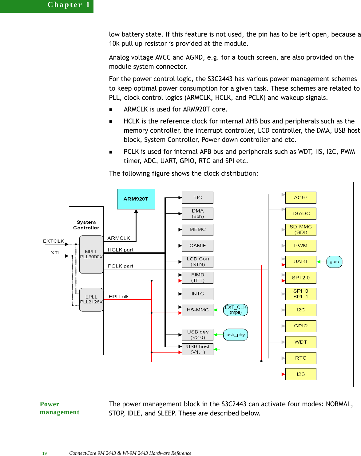
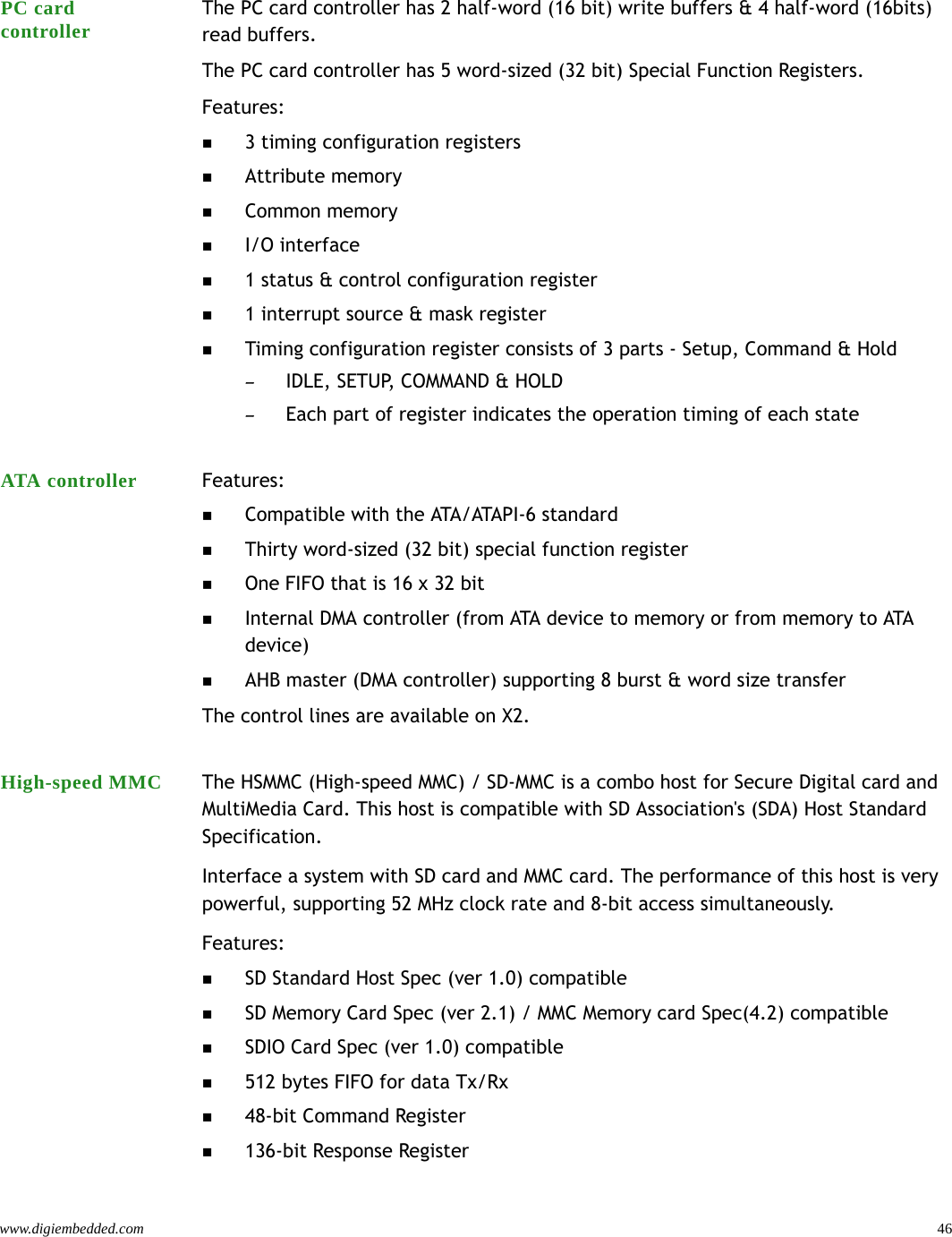
![21 ConnectCore 9M 2443 & Wi-9M 2443 Hardware ReferenceChapter 1The other power source supplies the CPU and internal logic, and should be controlled for power on/off. In SLEEP mode, the second power supply source for the CPU and internal logic will be turned off. The wake-up from SLEEP mode can be issued by EINT[15:0].In SLEEP mode, VDDi, VDDiarm, VDDMPLL and VDDEPLL will be turned off, and are controlled by PWREN. If the PWREN signal is activated (H), VDDi and VDDiarm are supplied by an external voltage regulator. If PWREN pin is inactive (L), VDDi and VDDiarm are turned off.In Power_OFF mode 1.2V have to be supplied to the VDD alive pin, and it is also necessary to provide the I/O-voltages of 1.8V/3.3V. Therefore the LDO, which supplies VDD alive will not be switched off.The following describes the sequence of entering SLEEP mode:1One of the SLEEP Mode entering events is triggered by the system software or by the hardware.2System controller requests bus controller to finish pending transaction.3Bus controller sends acknowledgement to system controller after bus transactions are completed.4System controller requests memory controller to enter self-refresh mode, preserving SDRAM contents.5System controller waits for self-refresh acknowledgement from memory controller.6After receiving the self-refresh acknowledge, disables the XTAL and PLL oscillation and also disables the external power source for the internal logic by asserting the PWR_EN pin to low state. The PWR_EN pin is the regulator disable control signal for the internal logic power source.The SLEEP mode exit sequence is as follows.1System controller enables external power source by deasserting PWR_EN to high state and initiates power settle down programmable through a register in the PWRSETCNT field of RSTCON register.2System controller releases the System Reset (synchronously, relatively to the system clock) after the power supply is stabilized.Wake-up event When S3C2443X wakes up from the STOP Mode by an External Interrupt, an RTC alarm interrupt and other interrupts, the PLL is turned on automatically. The initial-state of S3C2443X after wake-up from the SLEEP Mode is almost the same as the Power-On-Reset state except for the contents of the external DRAM is preserved. In contrast, S3C2443X automatically recovers the previous working state after wake-up from the STOP Mode. The following table shows the states of PLLs and internal clocks after wake-ups from the power-saving modes.](https://usermanual.wiki/Digi/50M1663/User-Guide-1175031-Page-21.png)
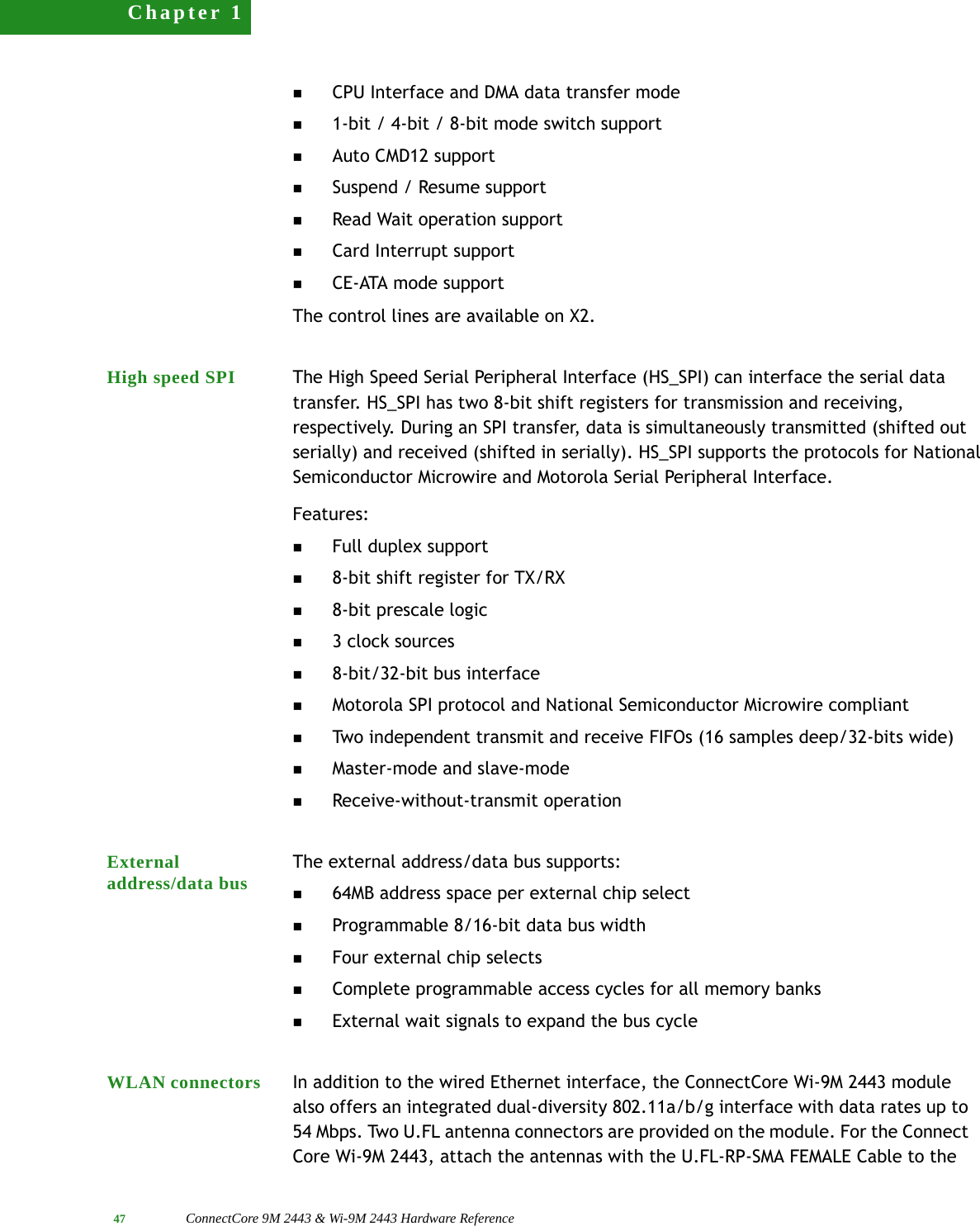
![25 ConnectCore 9M 2443 & Wi-9M 2443 Hardware ReferenceChapter 1At the module a pull up resistor is provided on the DEBUGEN# signal. Therefore only a jumper to GND is necessary on the base board.. . . . . . . . . . . . . . . . . . . . . . . . . . . . . . . . . . . . . . . . . . . . . . . . . . . . . . . . . . . . . . . . . . . . . . . . . . . . . . . . . .Chip selectsChip select memory map Name CPU Signal name Pin Address Range Size [Mb] Usage CommentsSCS0# SCS0# H15 0x3000_0000-0x37FF_FFFF128 SDRAM bank 0 First bank on moduleSCS1# SCS1# D17 0x3800_0000-0x3FFF_FFFF128 SDRAM bank 1RCS0# RCS0# A2 0x0000_0000-0x03FF_FFFF64 not availableRCS1# RCS1# A1 0x0800_0000-0x083F_FFFF64 external, RCS1#RCS2# RCS2# B3 0x1000_0000-0x103F_FFFF64 external, RCS2#RCS3# RCS3# C1 0x1800_0000-0x183F_FFFF64 external, RCS3#RCS4# RCS4# C4 0x2000_0000-0x203F_FFFF64 external, RCS4#RCS5# RCS5# E4 0x2800_0000-0x283F_FFFF64 internal, RCS5# Used for Ethernet Controller](https://usermanual.wiki/Digi/50M1663/User-Guide-1175031-Page-25.png)
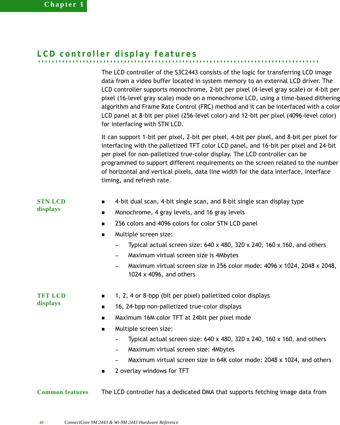
![27 ConnectCore 9M 2443 & Wi-9M 2443 Hardware ReferenceChapter 1Port B Selectable Pin Functions On module, default used as GPB10 Input/Output nXDREQ0 XDREQ0 InputGPB9 Input/Output nXDACK0 XDACK0 InputGPB8 Input/Output nXDREQ1 XDREQ1 InputGPB7 Input/Output nXDACK1 XDACK1 InputGPB6 Input/Output nXBREQ XBREQ InputGPB5 Input/Output nXBACK XBACK InputGPB4 Input/Output TCLK - InputGPB3 Input/Output TOUT3 - not used, reservedGPB2 Input/Output TOUT2 - InputGPB1 Input/Output TOUT1 - InputGPB0 Output only TOUT0 - InputPort C Selectable Pin Functions On module, default used asGPC15 Input/Output VD7 - VD7GPC14 Input/Output VD6 - VD6GPC13 Input/Output VD5 - VD5GPC12 Input/Output VD4 - VD4GPC11 Input/Output VD3 - VD3GPC10 Input/Output VD2 - VD2GPC9 Input/Output VD1 - InputGPC8 Input/Output VD0 - InputGPC7 Input/Output LCD_VF[2] - LCD_VF[2]GPC6 Input/Output LCD_VF[1] - LCD_VF[1]GPC5 Input/Output LCD_VF[0] - LCD_VF[0]GPC4 Input/Output VM - VMGPC3 Input/Output VFRAME - VFRAMEGPC2 Input/Output VLINE - VLINEGPC1 Input/Output VCLK - OutputGPC0 Input/Output LEND - Input](https://usermanual.wiki/Digi/50M1663/User-Guide-1175031-Page-27.png)
![www.digiembedded.com 383. Auto (Sequential) X/Y Position Conversion Mode is activated as follows:1Touch Screen Controller sequentially converts the X-Position or Y-Position that is touched. 2After touch controller writes X-measurement data to ADCDAT0 and writes Y-measurement data to ADCDAT1, the Touch Screen Interface generates Interrupt source to Interrupt Controller in Auto Position Conversion Mode.4. Waiting for Interrupt Mode is activated as follows:1The Touch Screen Controller generates an interrupt (INT_TC) signal when the stylus is down. Waiting for Interrupt Mode setting value is rADCTSC=0xd3; // XP_PU, XP_Dis, XM_Dis, YP_Dis, YM_En. 2After the Touch Screen Controller generates interrupt signal (INT_TC), the user must wait for the interrupt mode to be cleared (XY_PST sets to the No operation Mode).5. Standby Mode Standby Mode is activated when ADCCON [2] is set to '1.' In this mode, A/D conversion operation is halted and ADCDAT0, ADCDAT1 register contains the previous converted data.Reset controller On the module there is an Analog Devices ADM811SARTZ used. This device monitors 3.3V and has RSTIN# as debounced manual reset input and through a series resistor of 470R produces PWRGOOD as output. The voltage threshold is 2.93V. Reset output length is typically 240ms.JTAG The standard JTAG signals are provided at the system connector. A JTAG/Multi-ICE connector has to be provided at the base board for debugging.The signal DEBUGEN# (CONF0) from the base board to the module is necessary, to be able to switch on and off a connection between the system reset and the JTAG reset.The pull-up resistors, belonging to the JTAG interface, are placed on the module.Common features The LCD controller has a dedicated DMA that supports to fetch the image data from video buffer located in system memory. Its features also include:Dedicated interrupt functions (INT_FrSyn and INT_FiCnt)The system memory is used as the display memorySupports Multiple Virtual Display Screen (Supports Hardware Horizontal/Vertical Scrolling)Programmable timing control for different display panelsSupports little and big-endian byte ordering, as well as WinCE data formats](https://usermanual.wiki/Digi/50M1663/User-Guide-1175031-Page-38.png)
![45 ConnectCore 9M 2443 & Wi-9M 2443 Hardware ReferenceChapter 1(TCMPBn) has an initial value which is loaded into the compare register to be compared with the down-counter value. This double buffering feature of TCNTBn and TCMPBn makes the timer generate a stable output when the frequency and duty ratio are changed.Each timer has its own 16-bit down counter, which is driven by the timer clock. When the down counter reaches zero, the timer interrupt request is generated to inform the CPU that the timer operation has been completed. When the timer counter reaches zero, the value of corresponding TCNTBn is automatically loaded into the down counter to continue the next operation. However, if the timer stops, for example, by clearing the timer enable bit of TCONn during the timer running mode, the value of TCNTBn will not be reloaded into the counter.The value of TCMPBn is used for pulse width modulation (PWM). The timer control logic changes the output level when the down-counter value matches the value of the compare register in the timer control logic. Therefore, the compare register determines the turn-on time (or turn-off time) of a PWM output.Features:Five 16-bit timersTwo 8-bit prescalers & Two 4-bit dividerProgrammable duty control of output waveform (PWM)Auto reload mode or one-shot pulse modeDead-zone generatorAll of the Timer outputs are connected to the system connector.Clock output At the global pins of the system connector there is a clock signal available (BCLKOUT0), which is buffered by a clock buffer and can be chosen to be either MPLL CLK, EPLL CLK, FCLK, HCLK, PCLK or DCLK. The source of this clock signal is the CLKOUT0 port at the CPU, which can be programmed to different clocks, by the CLKSEL0 register.The following table shows the bits [6:4] of the CLKSEL0 register:CF/ATA The single-slot CF controller consists of 2 parts - PC card controller & ATA controller. They are multiplexing from or to PAD signals. Users can select either PC card or True-IDE mode operation. Default mode is PC card mode. The CF controller has a top level SFR with card power enable bit, output port enable bit & mode select (True-IDE or PC card) bit.CLKSELO [6.4] 000 001 010 011 100 101 11xCLKOUT0 MPLL CLK EPLL CLK FCLK HCLK PCLK DCLK0 Reserved](https://usermanual.wiki/Digi/50M1663/User-Guide-1175031-Page-45.png)
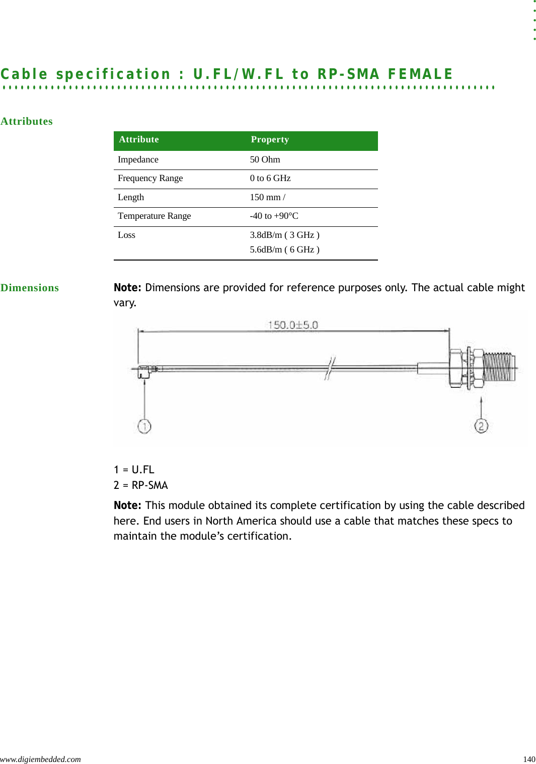
![www.digiembedded.com 48primary connector [X5] and the secondary connector [X4] on the module. You must use only this cable and antennas to carry on the module.Note When disconnecting U.FL connectors, the use of U.FL plug extraction tool (Hirose P/N U.FL-LP-N-2 or U.FL-LP(V)-N-2) is strongly recommended to avoid damage to the U.FL connectors on the ConnectCore Wi-9M 2443 module.To mate U.FL connectors, the mating axes of both connectors must be aligned. The "click" will confirm fully mated connection. Do not attempt insertion at an extreme angle.](https://usermanual.wiki/Digi/50M1663/User-Guide-1175031-Page-48.png)
![www.digiembedded.com 54X1-72 TOUT1 I/O TOUT1GPB1Timer outX1-73 NC I/O WLAN_DISABLE# Not connected; reserved for CCW9MX1-74 NC I/O WLAN_LED# Not connected; reserved for CCW9MX1-75 SDCLK I/O SD0_CLKGPE5AC_BIT_CLKSD-interfaceX1-76 SDCMD I/O SD0_CMDGPE6AC_SDISD-interfaceX1-77 SDDATA0 I/O SD0_DAT[0]GPE7AC_SDOSD-interfaceX1-78 SDDATA1 I/O SD0_DAT[1]GPE8AC_SYNCSD-interfaceX1-79 GND P GNDX1-80 SDDATA2 I/O SD0_DAT[2]GPE9AC_RESETSD-interfaceX1-81 SDDATA3 I/O SD0_DAT[3]GPE10SD-interfaceX1-82 EINT0 I/O EINT0GPF0External interruptsX1-84 TOUT2 I/O TOUT2GPB2Timer outX1-85 SS1# I/O SS1GPL14SPI1 InterfaceX1-86 SPIMISO1 I/O SPIMISO1GPL12SPI1 InterfaceX1-87 SPIMOSI1 I/O SPIMOSI1GPL11SPI1 InterfaceX1-88 SPICLK1 I/O SPICLK1GPL10SPI1 InterfaceX1-89 EINT17 I/O EINT17GPG9General purpose input / outputX1-90 EINT1\SD_CD# I/O EINT1GPF1General purpose input / outputPin Signal Type Signal name Description](https://usermanual.wiki/Digi/50M1663/User-Guide-1175031-Page-54.png)
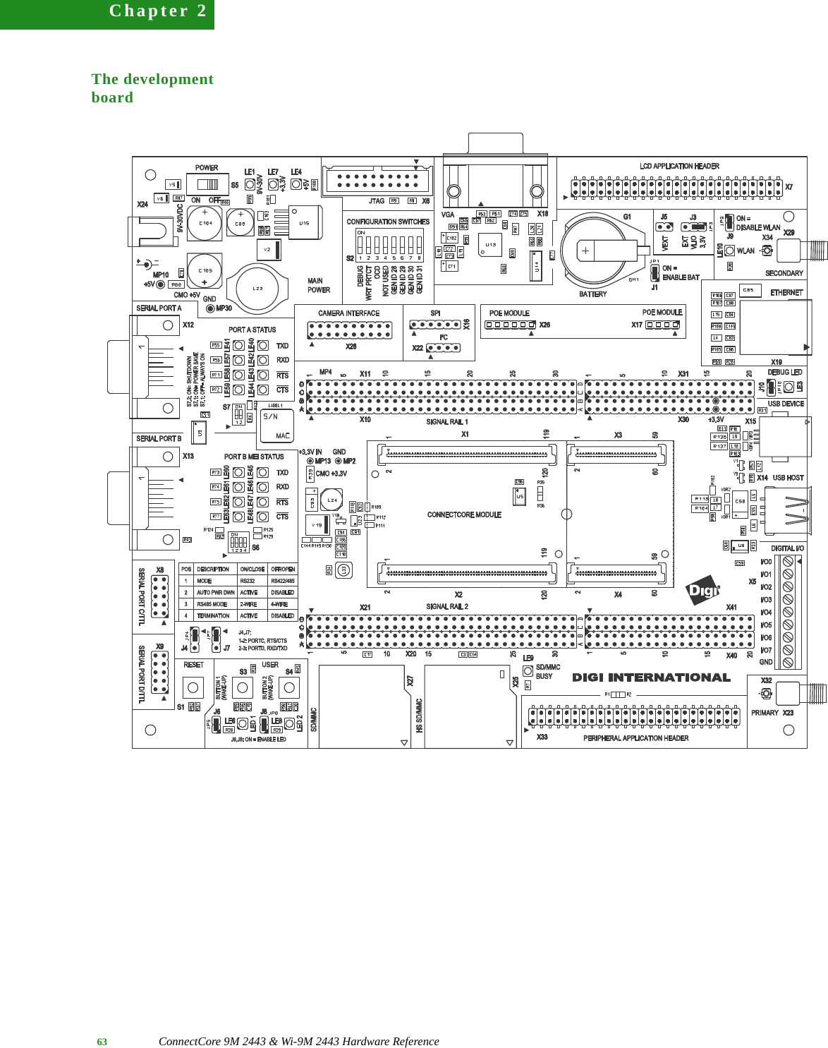
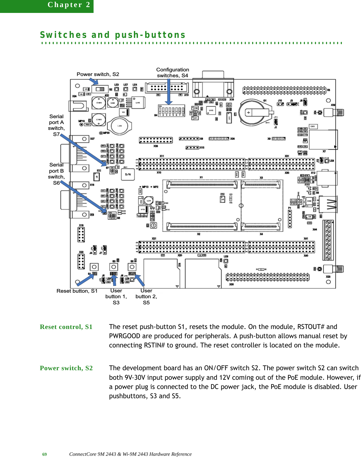
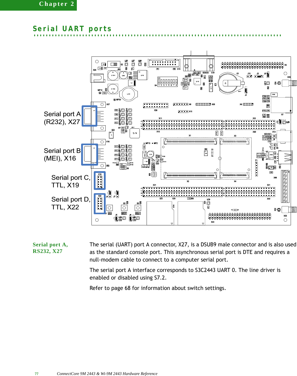
![. . . . .www.ConnectCore 9M 2443 & Wi-9M 2443 Hardware Reference.com 70Use the user push-buttons to interact with the applications running on the module. Use these module signals to implement the push-buttons:Legend for multi-pin switches Switches S4, S6, and S7 are multi-pin switches. In the description tables for these switches, the pin is designated as S[switch number].[pin number]. For example, pin 1 in switch 2 is specified as S4.1.Module configuration switches, S4Use S2 to configure the module:Serial port B MEI configuration switchesUse S6 to configure the line interface for serial port B MEI.Signal name Switch (pushbutton GPIO usedUSER_PUSH_BUTTON_1 S3 GPF0USER_PUSH_BUTTON_2 S5 GPF6Dip-switch positionUsage1 DEBUGEN#2 Reserved3OCD_EN4Reserved5 SW_CONF4Switch pin Function CommentsS6.1 On = RS232 transceiver enabledRS422/RS485 transceiver disabledOff= RS232 transceiver disabledRS422/RS485 transceivers enabledS6.2 On = Auto Power Down enabledOff = Auto Power Down disabledAuto Power Down is not supported on this board. This signal is only accessible to permit the user to completely disable the MEI interface for using signals for other purposes. To disable the MEI interface go in RS232 mode (S6.1 = ON) and activate the Auto Power Down feature (S6.2 = ON). Be sure that no cable is connected to connector X3.S6.3 On = 2 wire interface (RS422/RS485)Off = 4 wire interface (RS422)](https://usermanual.wiki/Digi/50M1663/User-Guide-1175031-Page-70.png)
![. . . . .www.ConnectCore 9M 2443 & Wi-9M 2443 Hardware Reference.com 108. . . . . . . . . . . . . . . . . . . . . . . . . . . . . . . . . . . . . . . . . . . . . . . . . . . . . . . . . . . . . . . . . . . . . . . . . . . . . . . . . .WLAN InterfaceFor the ConnectCore Wi-9M 2443, attach the antenna to the primary connector [X23] and the secondary connector [X34] on the development board. See figure below.](https://usermanual.wiki/Digi/50M1663/User-Guide-1175031-Page-108.png)