Hardware Reference Manual

ConnectCore™ 9M 2443
and Wi-9M 2443
Hardware Reference
90000952_B
Release date: August 2009

www.digiembedded.com
©2009 Digi International Inc.
All rights reserved.
Digi, Digi International, the Digi logo, a Digi International Company, Digi JumpStart Kit and ConnectCore are
trademarks or registered trademarks of Digi International, Inc. in the United States and other countries worldwide.
All other trademarks are the property of their respective owners.
All other trademarks mentioned in this document are the property of their respective owners.
Information in this document is subject to change without notice and does not represent a commitment on the part
of Digi International.
Digi provides this document “as is,” without warranty of any kind, either expressed or implied, including, but not
limited to, the implied warranties of fitness or merchantability for a particular purpose. Digi may make
improvements and/or changes in this manual or in the product(s) and/or the program(s) described in this manual at
any time.
This product could include technical inaccuracies or typographical errors. Changes are periodically made to the
information herein; these changes may be incorporated in new editions of the publication.

ConnectCore 9M 2443 & Wi-9M 2443 Hardware Reference

. . . . .
www.digiembedded.com
This guide provides information about the Digi ConnectCore 9M 2443 embedded
core module family. Visit the Digi support website:
www.digiembedded.com/support.
To access current technical documentation available for the S3C2443 processor,
please visit the Samsung website.
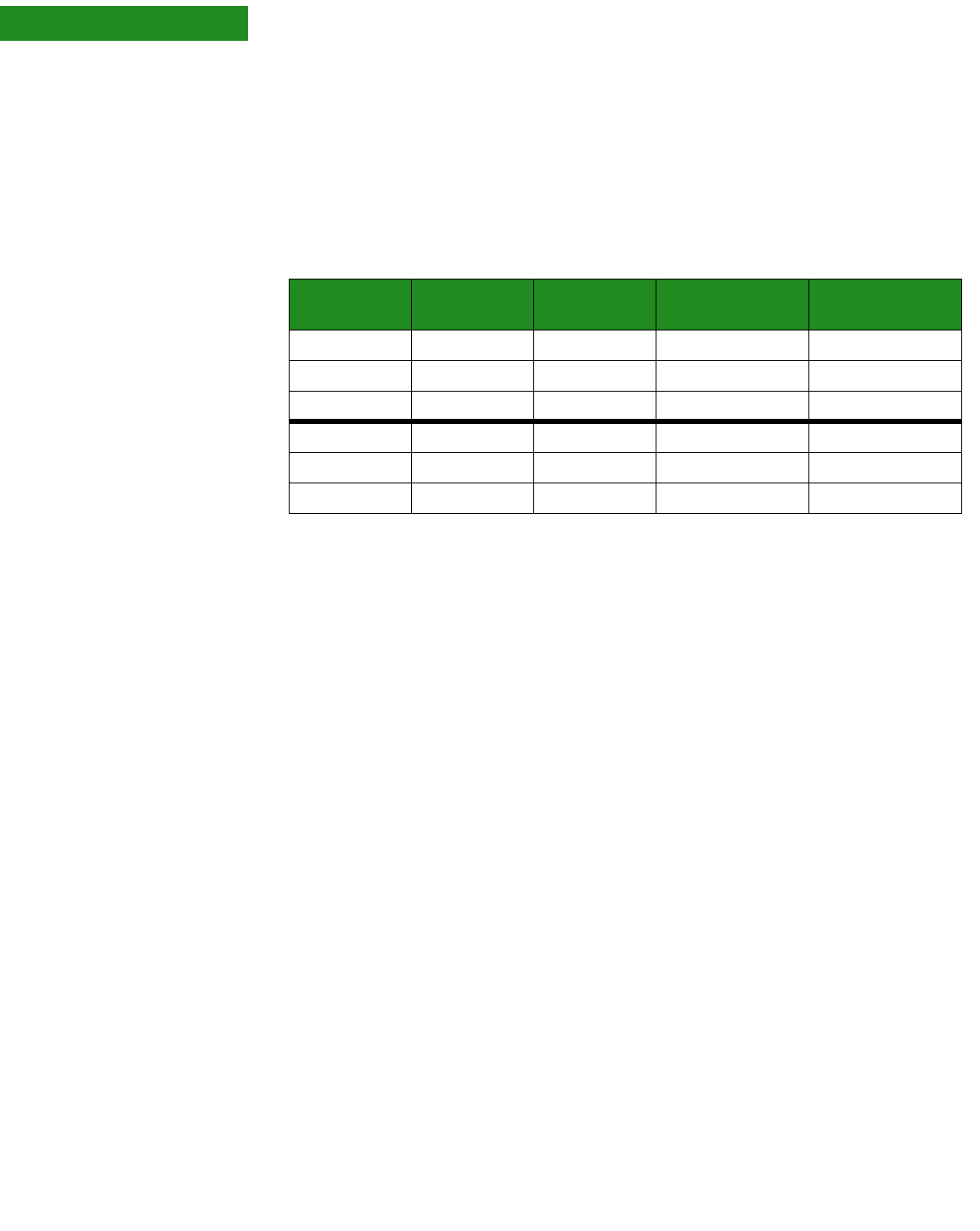
Conventions used
in this guide This table describes the typographic conventions used in this guide:
. . . . . . . . . . . . . . . . . . . . . . . . . . . . . . . . . . . . . . . . . . . . . . . . . . . . . . . . . . . . . . . . . . . . . . . . . . . . . . . . . .
Digi information
Documentation
updates Please always check the product specific section on the Digi support website for the
most current revision of this document: www.digiembedded.com/support.
. . . . . . . . . . . . . . . . . . . . . . . . . . . . . . . . . . . . . . . . . . . . . . . . . . . . . . . . . . . . . . . . . . . . . . . . . . . . . . . . . .
Change Log
Revision B Added WLan information for the ConnectCore Wi-9M 2443.
Added WLan information under environmental specifications in Appendix A.
Added a new drawing on page 136.
Made minor document updates.
This convention Is used for
italic type Emphasis, new terms, variables, and document titles.
monospaced type Filenames, pathnames, and code examples.

6ConnectCore 9M 2443 & Wi-9M 2443 Hardware Reference
Chapter 1
Contact
information For more information about your Digi products, or for customer service and
technical support, contact Digi International.
To contact Digi International by Use
Mail Digi International
11001 Bren Road East
Minnetonka, MN 55343
U.S.A
World Wide Web http://www.digiembedded.com/support/
email http://www.digiembedded.com/support/
Telephone (U.S.) (952) 912-3444 or (877) 912-3444
Telephone (other locations) +1 (952) 912-3444 or (877) 912-3444

Contents
. . . . . . . . . . . . . . . . . . . . . . . . . . . . . . . . . . . . . . . . . . . . . . . . . . . . . . . . . . . . . . . .
. . . . . . .
Change Log....................................................................................... 5
Revision B ................................................................................. 5
Chapter 1: About the Module ............................................................... 12
Features and functionality ...................................................................12
Block diagrams .................................................................................16
CPU........................................................................................16
Module ....................................................................................17
Detailed module description .................................................................18
Configuration ............................................................................18
Power Supply ............................................................................18
Power management.....................................................................19
NORMAL mode ...........................................................................20
IDLE mode ................................................................................20
STOP mode ...............................................................................20
SLEEP mode ..............................................................................20
Wake-up event ..........................................................................21
Reset ......................................................................................22
Memory ..........................................................................................23
DDR SDRAM memory ....................................................................23
NAND Flash memory ....................................................................23
Configuration pins - CPU module ............................................................24
Chip selects .....................................................................................25
Chip select memory map ..............................................................25
Multiplexed GPIO pins .........................................................................26
S3C2443X Port Configuration..........................................................26
Interfaces .......................................................................................32
RTC ........................................................................................32
UART interface ..........................................................................32
SPI interface .............................................................................34
I2C interface .............................................................................35
USB interface ............................................................................35
Ethernet interface ......................................................................36
WLAN interface..........................................................................37
A/D converter and touch screen interface..........................................37
Touch screen interface modes ........................................................37
Reset controller .........................................................................38

8ConnectCore 9M 2443 & Wi-9M 2443 Hardware Reference
Chapter 2
JTAG ......................................................................................38
Common features .......................................................................38
Watchdog timer .........................................................................39
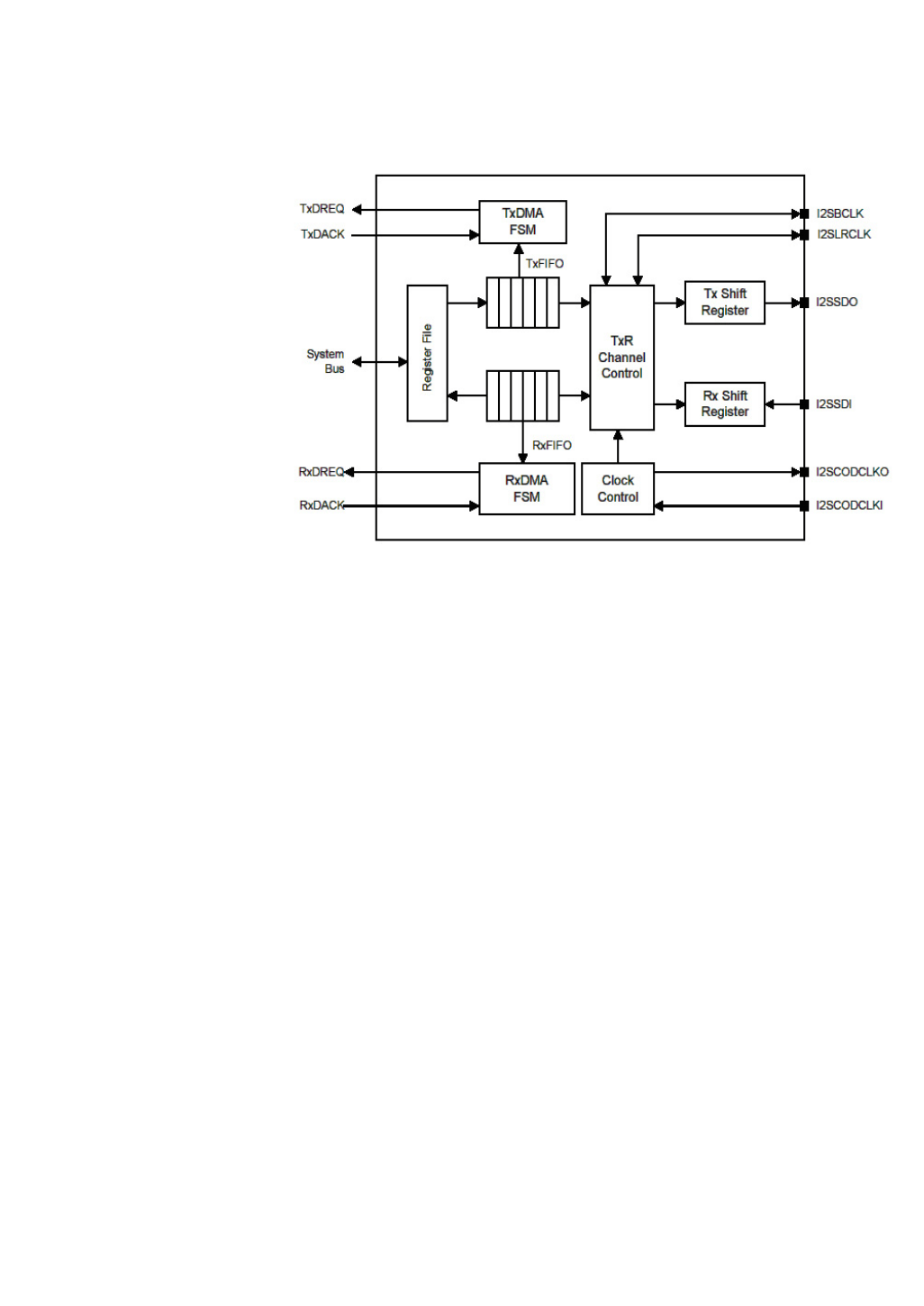
IIS-Bus interface .........................................................................39
IIS block diagram: .......................................................................40
IIS-Bus format............................................................................40
Camera interface........................................................................41
.............................................................................................41
AC97 Controller..........................................................................42
SD host interface ........................................................................44
PWM timer................................................................................44
Clock output .............................................................................45
CF/ATA....................................................................................45
PC card controller.......................................................................46
ATA controller ...........................................................................46
High-speed MMC .........................................................................46
High speed SPI ...........................................................................47
External address/data bus.............................................................47
WLAN connectors........................................................................47
LCD controller display features ..............................................................49
STN LCD displays ........................................................................49
TFT LCD displays ........................................................................49
Common features .......................................................................49
Module pinout ..................................................................................50
System connector X1 ...................................................................50
System connector X2 ...................................................................56
Configuration pins - CPU ......................................................................61
Chapter 2: About the Development Board .........................................62
What’s on the development board? ..................................................62
The development board................................................................63
User interface ..................................................................................64
Power management.....................................................................64
General information ...........................................................................64
Power supply.............................................................................64
3.3VDC power controller - VLIO.......................................................65
Power LEDs ...............................................................................65
Coin cell for RTC ........................................................................65
Current measuring option..............................................................65
Reset ......................................................................................65
JTAG interface ..........................................................................65
I²C interface .............................................................................65
PoE connectors ..........................................................................65
Peripheral application connector.....................................................66
LCD Application Kit Connector ........................................................66

. . . . .
www.digiembedded.com 9
VGA interface ........................................................................... 66
UARTs .................................................................................... 66
UART A - console ....................................................................... 66
UART B - UART / MEI................................................................... 66
UART C - TTL interface ................................................................ 66
UART D - TTL interface ................................................................ 66
SPI interface(s) ......................................................................... 67
Camera interface.............................................................................. 68
Switches and push-buttons .................................................................. 69
Reset control, S1 ....................................................................... 69
Power switch, S2 ....................................................................... 69
Legend for multi-pin switches........................................................ 70
Module configuration switches, S4................................................... 70
Serial port B MEI configuration switches............................................ 70
Test points ..................................................................................... 71
Numbers and description.............................................................. 71
Factory default interface configuration for development board ...................... 72
LEDs ............................................................................................. 73
WLAN, LE10.............................................................................. 73
Power LEDs, LE1, LE4, and LE7....................................................... 73
User LEDs, LE5 and LE6 ................................................................ 74
Serial status LEDs....................................................................... 74
Status LEDs Serial port A .............................................................. 75
Status LEDs Serial port B .............................................................. 75
Debug, LE3 .............................................................................. 75
Battery and battery holder .................................................................. 76
Serial UART ports.............................................................................. 77
Serial port A, RS232, X27.............................................................. 77
Serial port B, MEI interface, X16..................................................... 79
Serial port C, TTL interface, X19 .................................................... 79
Serial port D, TTL interface, X22 .................................................... 80
I2C interface ................................................................................... 81
I2C connector, X22 ..................................................................... 81
SPI interface ................................................................................... 82
X8-SPI connector........................................................................ 83
Current Measurement Option................................................................ 84
Measurement options .................................................................. 84
How the CMO works .................................................................... 85
PoE module connectors - IEEE802.3af...................................................... 86
The PoE module ........................................................................ 87
PoE connector (power in), X17 ....................................................... 87
PoE connector (power out), X26 ..................................................... 87
POE_GND................................................................................. 87
VGA connector ................................................................................. 88
VGA connector, X18.................................................................... 88

10 ConnectCore 9M 2443 & Wi-9M 2443 Hardware Reference
Chapter 2
USB connectors .................................................................................90
USB device connector, X15 ............................................................90
USB host connector, X14 ...............................................................90
Digital I/O .......................................................................................91
I2C digital I/O expansion, X44 ........................................................91
JTAG interface .................................................................................92
Standard JTAG ARM connector, X13..................................................93
Peripheral (extension) headers ..............................................................94
LCD application header, X5............................................................95
Peripheral application header, X3....................................................96
Module connectors and signal rails ..........................................................97
Signal rails................................................................................97
X10 pinout ................................................................................98
X11 pinout ................................................................................99
X20 pinout .............................................................................. 100
X21 pinout .............................................................................. 101
Power connector ............................................................................. 102
Jumpers ....................................................................................... 103
Jumpers................................................................................. 104
Ethernet interface ........................................................................... 105
RJ-45 pin allocation, X7 .............................................................. 106
WLAN Interface............................................................................... 108
Interfaces without special connectors.................................................... 109
ADC signals ............................................................................. 109
CF signals ............................................................................... 109
I2S/AC97 signals ....................................................................... 110
SPI1 signal .............................................................................. 110
Module and test connectors ................................................................ 111
X1 pinout ............................................................................... 111
X2 pinout ............................................................................... 121
Network interface ........................................................................... 128
WLAN interface............................................................................... 128
Environmental specifications............................................................... 130
ConnectCore
9M 2443 ................................................................................. 130
ConnectCore
Wi-9M 2443 ............................................................................. 130
Thermal specifications ...................................................................... 131
Standard Operating Temperature Ranges ......................................... 131
recommendations ..................................................................... 132
Power requirements ......................................................................... 133
Typical Power Requirements ............................................................... 133
ConnectCore 9M 2443 ................................................................ 133
ConnectCore “Wi-9M 2443”.......................................................... 134
Mechanical specifications................................................................... 136

. . . . .
www.digiembedded.com 11
ConnectCore 9M 2443................................................................. 136
ConnectCore
Wi-9M 2443 ............................................................................. 138
Connector Reference Parts ................................................................. 139
Base Board Connector X1, X2 ........................................................139
Base Board Connector X3, X4 ........................................................139
Cable specification : U.FL/W.FL to RP-SMA FEMALE.................................... 140
Attributes...............................................................................140
Dimensions ............................................................................. 140
Antenna specification: 802.11a/b/g antenna............................................ 141
Attributes...............................................................................141
Dimensions ............................................................................. 141
Antenna Specification: 802.11b/g antenna .............................................. 142
Attributes...............................................................................142
Dimensions ............................................................................. 142
Polar Plots ..................................................................................... 143
Safety statements ............................................................................ 144
........................................................................................... 144
FCC Part 15 Class B .......................................................................... 145

www.digiembedded.com 12
About the Module
CHAPTER 1
The network-enabled ConnectCore 9M 2443 core module family delivers leading
performance, low power operation, and rich peripheral interface support for a wide
variety of applications, including medical devices, transportation, security/access
control, networked displays, and more.
The modules utilize an innovative and power-efficient Samsung S3C2443 processor
with up to 533 MHz and a multilayered memory bus architecture that allows
simultaneous data transfer between processor, memory and peripherals. This
optimized design eliminates the traditional bus bandwith bottlenecks that are
common on other platforms. For example, updating graphical information through
the LCD controller and retrieving relevant data from memory at the same time can
now be realized without compromising overall performance and user experience.
Designed from the ground up with power budget conscious applications in mind, the
ConnectCore 9M 2443 module family is an ideal system platform for mobile and
battery-operated product designs with full off-the-shelf hard- and software support
for all power management modes. The modules also offer a wide variety of on-
board peripherals such as network connectivity options, a TFT/CSTN LCD controller,
camera interface, audio codec interfaces, hi-speed USB device, full-speed USB host,
high-speed memory card support, external mass storage, and other interfaces.
. . . . . . . . . . . . . . . . . . . . . . . . . . . . . . . . . . . . . . . . . . . . . . . . . . . . . . . . . . . . . . . . . . . . . . . . . . . . . . . . . .
Features and functionality
32-bit Samsung S3C2443 processor
ARM920T core at 400/533 MHz
16 KB of instruction/data cache
Up to 133 MHz memory bus speed
Up to 1 GB of NAND Flash
Up to 256 MB DDR SDRAM

13 ConnectCore 9M 2443 & Wi-9M 2443 Hardware Reference
Chapter 1
LCD controller (CSTN/TFT)
Up 1024x1024 pixels resolution
Up to 16 grey levels/4096 colors (STN)
Up to 24 bpp, two overlay windows (TFT)
Camera interface
ITU-R BT 601/656 8-bit mode support
4096x4096 pixels / 2048x2048 scaling
Mirror, 180° rotation, digital zoom in
RGB 16/24-bit, YCbCr 4:2:0/4:2:2 output
I2S and AC’97 audio codec controllers
USB support with integrated PHYs
USB 2.0 device, 1-port, high-/full-speed
USB 1.1 host, 2-port, low-/full-speed
Ethernet interface
–10/100 Mbit Ethernet MAC and PHY
WLAN interface
–802.11a/b/g WLAN interface with dual-diversity antenna setup
4-channel UART
Up to 921 kbps, IrDA 1.0 SIR mode
2-port SPI/Single-port HS-SPI
Master and slave mode
Up to 33 MHz
I2C-Bus Interface
1-ch Multi-Master IIC-Bus
Serial, 8-bit oriented and bi-directional data transfers up to 100 Kbit/s in
Standard mode or up to 400 Kbit/s in fast mode

www.digiembedded.com 14
SD/SDIO/MMC
1-/4-bit and block/stream, up to 25 MHzHigh-Speed (HS) MMC
SD HC 1.0, SD MC 2.1, SDIO 1.0, MMC 4.2
1-/4-/8-bit modes, up to 50 MHz
CE-ATA mode support
CF/ATA
Compact Flash 3.0 PC card mode
ATA/ATAP I-6 mode with PIO/UDMA
10-bit ADC & Touch Screen Interface
10-channel multiplexed, 500k samples/s
Timers/PWM
4-ch 16-bit timer/PWM, 1-ch 16-bit internal
8-/16-bit external memory bus interface
Power management modes
Normal, idle, stop, and sleep
Ext IRQ, RTC alarm, tick interrupt wake-up
GPIO options
Up to 15 external IRQs
Up to 134 GPIOs
Watchdog Timer (16-bit)
Real-time clock with calendar function
Two 120-pin board-to-board connectors
15 ConnectCore 9M 2443 & Wi-9M 2443 Hardware Reference
Chapter 1
JTAG signals available on module connectors
Standard module variants
The ConnectCore 9M 2443 module is currently available in the standard variants
below.
* See section "Thermal specifications" in this document for details.
Please visit the Digi website, www.digiembedded.com/support, or contact Digi for
additional population options.
Speed Flash SDRAM Operating
temperature P/N
533 MHz 128 MB 64 MB -40 to 85C CC-9M-NA37-Z1
533 MHz 64MB 32 MB -40 to 85C CC-9M-NA26-Z1
400 MHz 64 MB 32 MB -20 to 70C CC-9M-QA25-Z1
533 MHz 128 MB 64 MB -40 to 65C* CC-W9M-NA37-XE
533 MHz 64MB 32 MB -40 to 65C* CC-W9M-NA26-XE
400 MHz 64 MB 32 MB -20 to 65C* CC-W9M-QA25-XE
www.digiembedded.com 16
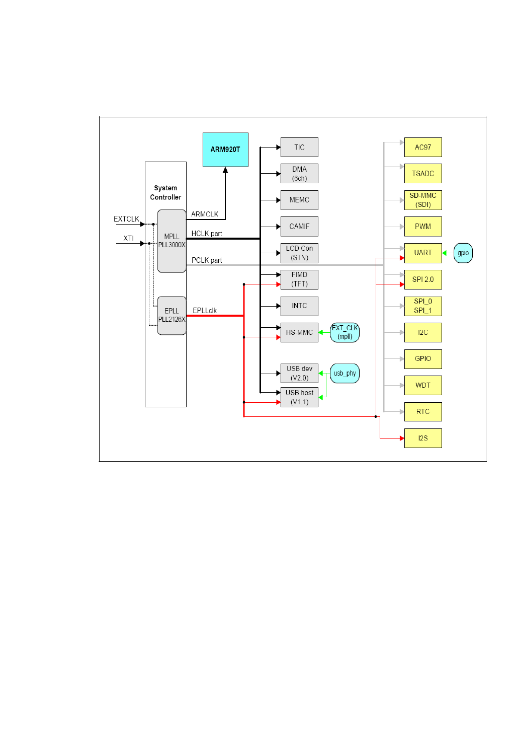
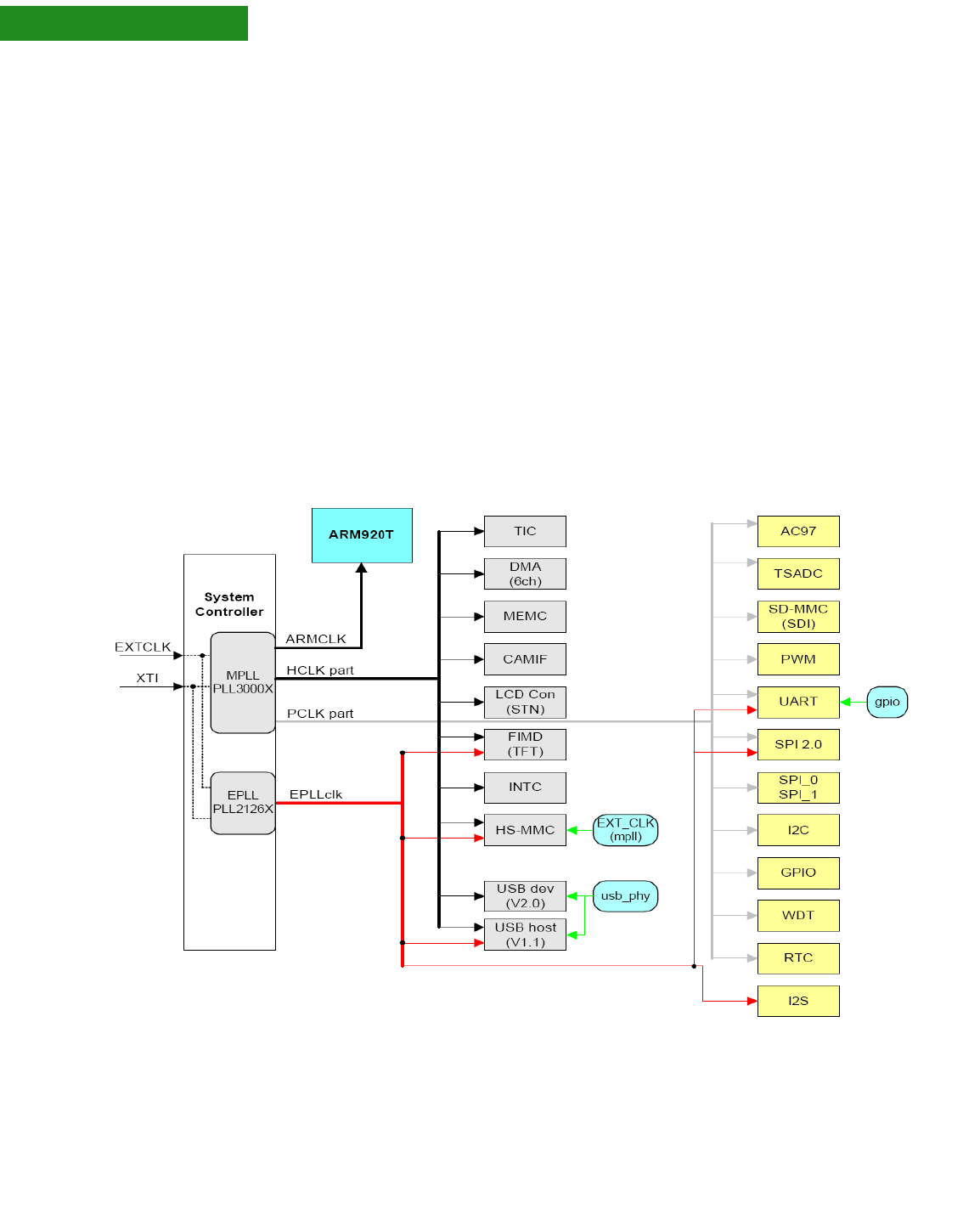
. . . . . . . . . . . . . . . . . . . . . . . . . . . . . . . . . . . . . . . . . . . . . . . . . . . . . . . . . . . . . . . . . . . . . . . . . . . . . . . . . .
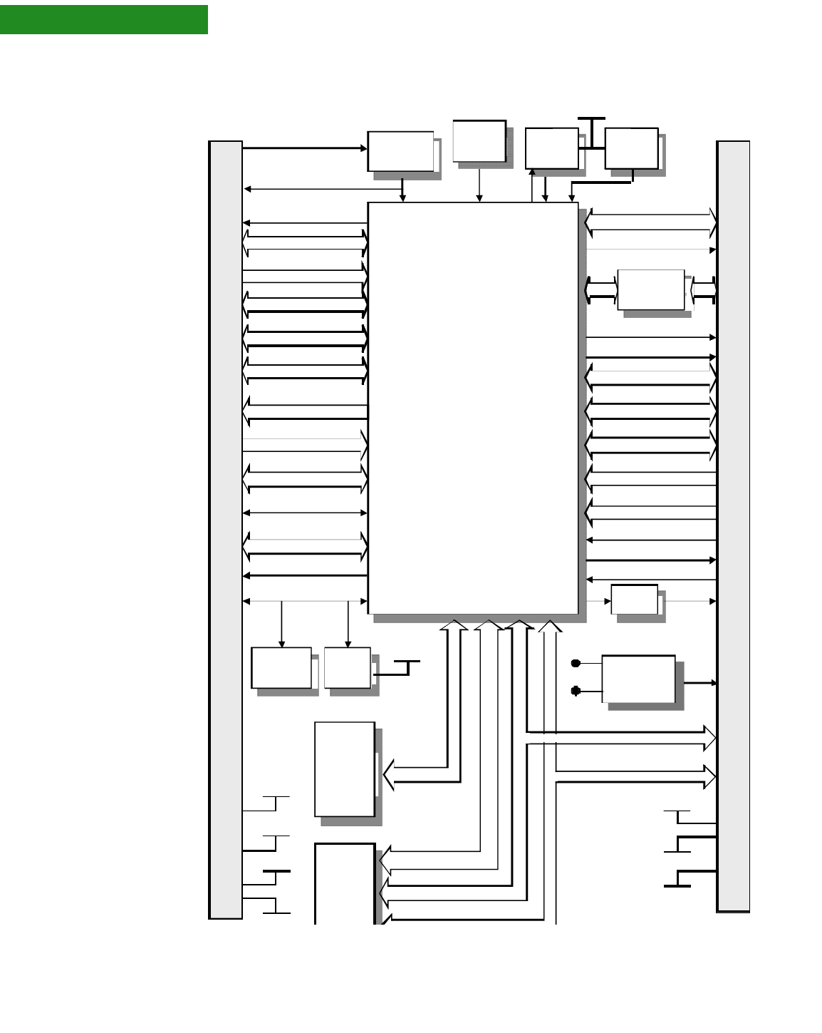
Block diagrams
CPU
17 ConnectCore 9M 2443 & Wi-9M 2443 Hardware Reference
Chapter 1
Module
S3C2443
Et he rn et -I/ F,
PHY
120pi n
Conn 1
2 b an k s
DDR
SDRAM
NAND
Flash
Reset
Generator
Flash Control
Address Bus
Dt B
COM 0/COM 1
JTAG
+3.3V
GND
RSTOUT#
RSTIN#
120pin
Conn 2
PW RGOOD
GND
VRTC
LEDLNK
LEDH0
Configuratio n
LCD/TF T-I/F
Bus Control
USB host1/device0
USB Detect/PWR Enable
Clock
Serial
EE P ROM
Ext. INT
AGND
AVCC
I2C
SP I
Timer Out
Address Bus
Data Bus
AC97/ I2S -I/F
SD-I/F
DMA
Analog In
Touch Screen
Timer In
PW R Enable Core
USB host0
USB PWR Enable
Buffer CLKOUT
RTC
VLIO
VRTC
Core
Voltag e
VLIO
Battery Fault
Camera-I/F
PLL
Volt ag e
SDRAM l/F
Wireless
PRIM. Antenna
SEC. Antenna
LED

www.digiembedded.com 18
. . . . . . . . . . . . . . . . . . . . . . . . . . . . . . . . . . . . . . . . . . . . . . . . . . . . . . . . . . . . . . . . . . . . . . . . . . . . . . . . . .
Detailed module description
Configuration The ConnectCore 9M 2443 Module supports 8 configuration pins:
4 pins provided for software configuration, which are routed to standard pin
locations on the development board (CONF[7:4]).
4 pins provided for hardware configuration, routed to the base board at
standard pin locations, including debug enable (DEBUG_EN#) and NAND flash
write protect (NAND_FWP#).
Power Supply The common power supply for the module is 3.3VDC. VLIO has to be connected to
3.3V on the base board.
The CPU specific core voltage of 1.2V@300MHz (1.3V@400MHz) and the voltage for
VDD alive will be generated on the module from the VLIO input, while the voltage for
memory power supply and I/OS is fed directly from the 3.3V.
The following requirements have to be met by the power supply:
The voltage at pin RTCVDD has been connected to 3.3V, even though the RTC is not
used. If VDD_RTC is not used, it has to be high (VDD_RTC=3.3V).
The S3C2443 supports DVS (dynamic voltage scaling). This means that the core
voltage may be reduced to 1V in idle mode while clock frequency is also reduced.
VRTC is used to connect a battery on the base board for the external RTC on the
module. If the external RTC is not used, pin VRTC doesn't need to be connected. VRTC
is only used to power the external RTC on the module.
If a battery supplies the power for the module, the pin BATT_FLT# can be connected
to a comparator output on the base board. The comparator may supervise the battery
voltage on the base board. The CPU does not wake up at power-off mode in case of
Power Supply @400MHz @533MHz
Module Power Supply 3.3V 3.3V ±5% 3.3V ± 5%
Module Power Supply VLIO 3.3V ±5% 3.3V ±5%
Core Voltage 1.3V (1.25V - 1.35V) 1.375 (1.325V - 1.425V)
VDD alive 1.15V - 1.35V 1.15V - 1.2V
Voltage for internal RTC 3V (1.8V - 3.6V) 3V (1.8V - 3.6V)
Power Supply for ext. RTC
VRTC 3V (e.g. Li-Battery) 3V (e.g. Li-Battery)
Analog Voltage 3.3V (3V - 3.6V) 3.3V (3V - 3.6V)
VIN at common CPU pins -0.3V - 3.3V ± 0.3V -0.3V - 3.3V ± 0.3V
19 ConnectCore 9M 2443 & Wi-9M 2443 Hardware Reference
Chapter 1
low battery state. If this feature is not used, the pin has to be left open, because a
10k pull up resistor is provided at the module.
Analog voltage AVCC and AGND, e.g. for a touch screen, are also provided on the
module system connector.
For the power control logic, the S3C2443 has various power management schemes
to keep optimal power consumption for a given task. These schemes are related to
PLL, clock control logics (ARMCLK, HCLK, and PCLK) and wakeup signals.
ARMCLK is used for ARM920T core.
HCLK is the reference clock for internal AHB bus and peripherals such as the
memory controller, the interrupt controller, LCD controller, the DMA, USB host
block, System Controller, Power down controller and etc.
PCLK is used for internal APB bus and peripherals such as WDT, IIS, I2C, PWM
timer, ADC, UART, GPIO, RTC and SPI etc.
The following figure shows the clock distribution:
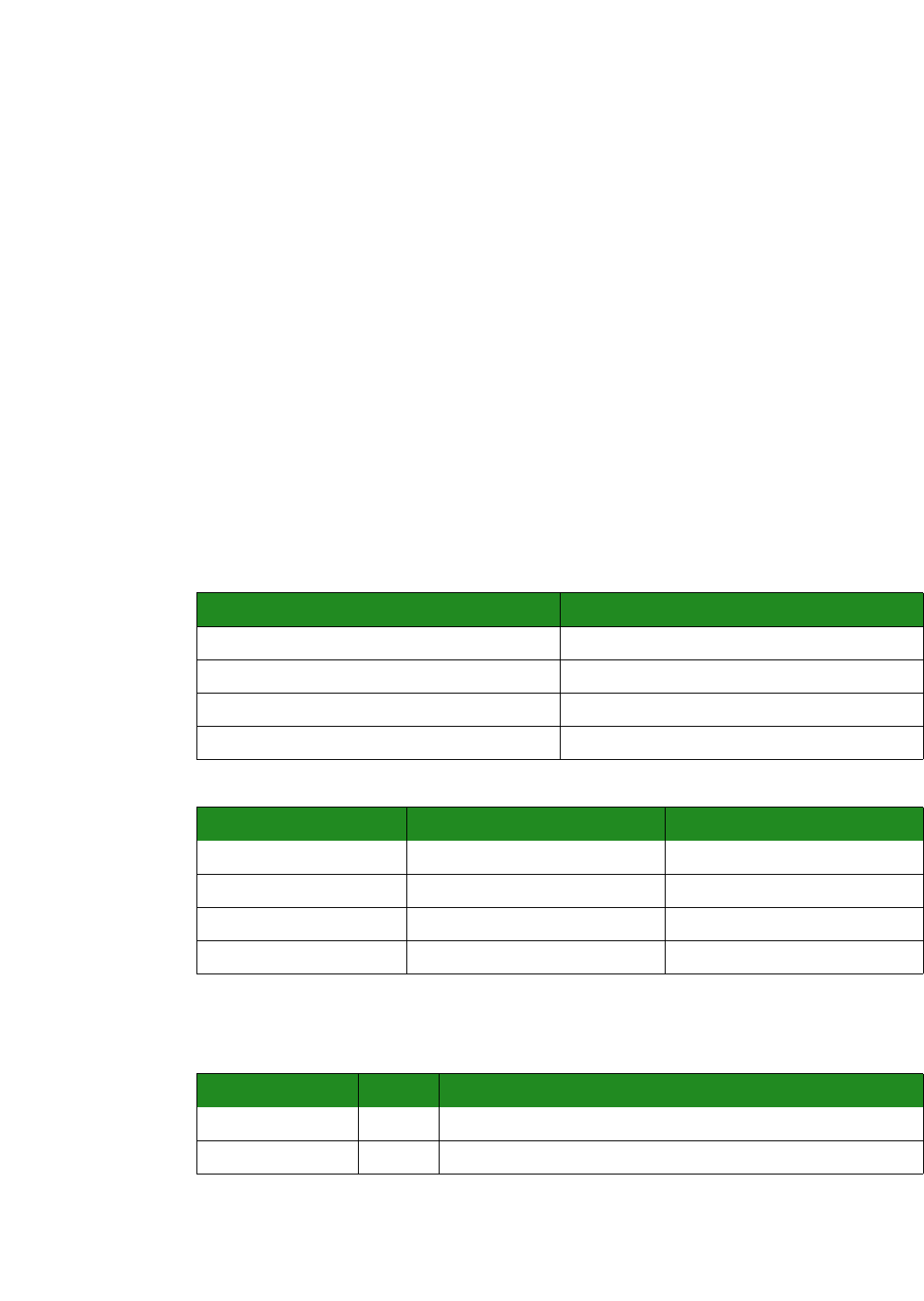
Power
management The power management block in the S3C2443 can activate four modes: NORMAL,
STOP, IDLE, and SLEEP. These are described below.

www.digiembedded.com 20
NORMAL mode In General Clock Gating mode, the On/Off clock gating of the individual clock
source of each IP block is performed by controlling each corresponding clock source
enable bit. The Clock Gating is applied instantly whenever the corresponding bit is
changed.
IDLE mode In IDLE mode, the clock to the CPU core is stopped. The IDLE mode is activated just
after the execution of the STORE instruction that enables the IDLE Mode bit. The
IDLE Mode bit should be cleared after wake-up from IDLE state.
STOP mode All clocks are stopped for minimum power consumption. Therefore, the PLL and
oscillator circuits are also stopped (oscillator circuit is controlled by PWRCFG
register). The STOP mode is activated after the execution of the STORE instruction
that enables the STOP mode bit. The STOP Mode bit should be cleared after wake-
up from STOP state.
To exit from STOP mode, external interrupt, RTC alarm, RTC Tick, or BATT_FLT has
to be activated. During the wake-up sequence, the crystal oscillator and PLL may
begin to operate. The crystal oscillator settle-down time and the PLL lock-time is
required for a stable ARMCLK and automatically inserted by the hardware of
S3C2443X. During these lock and settle-down times, no clock is supplied to the
internal logic circuitry.
The following describes the sequence initiating STOP mode:
1Set the STOP Mode bit (by the main CPU).
2System controller requests bus controller to finish pending transaction.
3Bus controller sends acknowledgement to system controller after bus
transactions are completed.
4System controller requests memory controller to enter self-refresh mode,
preserving SDRAM contents.
5System controller waits for self-refresh acknowledgement from memory
controller.
6After receiving the self-refresh acknowledge, system controller disables system
clocks, and switches SYSCLK source to MPLL reference clock.
7Disables PLLs and Crystal (XTI) oscillation. If OSC_EN_STOP bit in PWRCFG
register is 'high,' then system controller does not disable crystal oscillation.
Note: DRAM has to be in self-refresh mode during STOP and SLEEP mode to retain valid
memory data. LCD must be stopped before STOP and SLEEP mode, because DRAM can
not be accessed when it is in self-refresh mode.
SLEEP mode The block disconnects power to CPU, and the internal logic, with the exception of
the wake-up logic. Activating the SLEEP mode requires two independent power
sources. One of the two power sources supplies the power for the wake-up logic.

21 ConnectCore 9M 2443 & Wi-9M 2443 Hardware Reference
Chapter 1
The other power source supplies the CPU and internal logic, and should be
controlled for power on/off. In SLEEP mode, the second power supply source for the
CPU and internal logic will be turned off. The wake-up from SLEEP mode can be
issued by EINT[15:0].
In SLEEP mode, VDDi, VDDiarm, VDDMPLL and VDDEPLL will be turned off, and are
controlled by PWREN. If the PWREN signal is activated (H), VDDi and VDDiarm are
supplied by an external voltage regulator. If PWREN pin is inactive (L), VDDi and
VDDiarm are turned off.
In Power_OFF mode 1.2V have to be supplied to the VDD alive pin, and it is also
necessary to provide the I/O-voltages of 1.8V/3.3V. Therefore the LDO, which
supplies VDD alive will not be switched off.
The following describes the sequence of entering SLEEP mode:
1One of the SLEEP Mode entering events is triggered by the system software or by
the hardware.
2System controller requests bus controller to finish pending transaction.
3Bus controller sends acknowledgement to system controller after bus
transactions are completed.
4System controller requests memory controller to enter self-refresh mode,
preserving SDRAM contents.
5System controller waits for self-refresh acknowledgement from memory
controller.
6After receiving the self-refresh acknowledge, disables the XTAL and PLL
oscillation and also disables the external power source for the internal logic by
asserting the PWR_EN pin to low state. The PWR_EN pin is the regulator disable
control signal for the internal logic power source.
The SLEEP mode exit sequence is as follows.
1System controller enables external power source by deasserting PWR_EN to high
state and initiates power settle down programmable through a register in the
PWRSETCNT field of RSTCON register.
2System controller releases the System Reset (synchronously, relatively to the
system clock) after the power supply is stabilized.
Wake-up event When S3C2443X wakes up from the STOP Mode by an External Interrupt, an RTC
alarm interrupt and other interrupts, the PLL is turned on automatically. The initial-
state of S3C2443X after wake-up from the SLEEP Mode is almost the same as the
Power-On-Reset state except for the contents of the external DRAM is preserved. In
contrast, S3C2443X automatically recovers the previous working state after wake-
up from the STOP Mode. The following table shows the states of PLLs and internal
clocks after wake-ups from the power-saving modes.
www.digiembedded.com 22
To enter sleep mode by BATT_FLT, BATF_CFG bits of PWRCFG register must be
configured.
Do not exit from sleep mode when BATT_FLT is LOW; SLEEP_CFG bit of PWRCFG
register must be configured.
A Battery Fault Signal (BATT_FLT#) is provided at the CPU to recognize the battery
state of the battery at the base board, which powers the module. Therefore this pin
is routed to the system connector. At the base board a comparator has to supervise
the battery state and the output of the comparator delivers the BATT_FLT# signal.
The figure below shows the power management state diagram:
Reset There are 3 reset signals defined, which are routed to the system connector:
a reset input to the module (RSTIN#)
an output of the reset controller from the module (PWRGOOD)
a reset output from the CPU (RSTOUT#)
Mode before wake-up PLL on/off after wake-up SYSCLK after wake-up
and before the lock time SYSCLK after the lock
time by internal logic
IDLE Unchanged PLL output PLL output
STOP PLL state ahead of entering STOP
mode (PLL ON or not) PLL reference clock SYSCLK ahead of entering
STOP mode (PLL output or
not)
SLEEP Off PLL reference clock PLL reference (input) clock
Wake-up source Wake-up source
Reset or restricted
wake-up events

23 ConnectCore 9M 2443 & Wi-9M 2443 Hardware Reference
Chapter 1
RSTIN# signal from the base board is connected to the reset generator device
on the module. At the base board there could be a reset switch connected to
the RSTIN# signal. A 10k pull up resistor is connected to the RSTIN# signal on
the module.
PWRGOOD must be held to low level at least 4 FCLKs to recognize the reset
signal.
The low active reset of the reset controller is connected to the system via a 470R
series resistor.
RSTOUT# can be used for external device reset control. RSTOUT# is a function of
Watchdog Reset and Software Reset (RSTOUT# = PWRGOOD & WDTRST# &
SW_RESET).
. . . . . . . . . . . . . . . . . . . . . . . . . . . . . . . . . . . . . . . . . . . . . . . . . . . . . . . . . . . . . . . . . . . . . . . . . . . . . . . . . .
Memory
DDR SDRAM
memory On the module there are two banks provided for DDR SDRAM memory. Both banks can
support a 16-bit mobile DDR memory chip. Bank 1 provides one part of a 16bit DDR
SDRAM in a FBGA60 package, with 1.8V power supply.
Total size of memory is possible from 16MB (only one bank) up to 256MB (128MB each
bank).
Both banks have to be populated with equal devices since they share all control
signals with the exception of their chip selects.These are defined in the bank control
registers BANKCFG and BANKCON1-3 and Refresh Control Register.
NAND Flash
memory NAND Flash memory is provided, as a single Flash device. In order to support NAND
flash boot loader, the S3C2443 is equipped with an internal SRAM buffer called
Steppingstone. When booting, the first 4 KBytes of the NAND flash memory will be
loaded into Steppingstone and the boot code loaded into Steppingstone will be
executed.
Generally, the boot code will copy NAND flash content to DDR-SDRAM. Using hardware
ECC, the NAND flash data validity will be checked. Upon the completion of the copy,
the main program will be executed on the DDR-SDRAM.
Features:
NAND Flash memory I/F: Supports 512Bytes and 2KBytes Page.
Interface: 8-bit NAND flash memory interface bus.
Hardware ECC generation, detection and indication (Software correction).
www.digiembedded.com 24
SFR I/F: Supports Little Endian Mode, Byte/half word/word access to Data and
ECC Data register, and Word access to other registers.
Steppingstone I/F: Supports Little/Big Endian, Byte/half word/word access.
The Steppingstone 4-KB internal SRAM buffer can be used for another purpose
after NAND flash booting.
The write protect pin of the Flash device is routed to the hardware configuration
pin of the system connector FWP#. The device can be write protected at the base
board by connecting this pin to GND. At the module, a pull-up resistor is equipped.
. . . . . . . . . . . . . . . . . . . . . . . . . . . . . . . . . . . . . . . . . . . . . . . . . . . . . . . . . . . . . . . . . . . . . . . . . . . . . . . . . .
Configuration pins - CPU module
There are eight configuration pins provided on the system connector. Four of them
are provided as hardware configuration pins, and the other four can be used as
software configuration pins. A 10k pull up resistor is provided on each signal line of
the configuration pins.
The following pins on the connector are defined as hardware configuration pins:
The following port pins are defined as software configuration pins:
The signal DEBUGEN# (CONF0) from the base board to the module is necessary to
allow switching a connection on and off between the system reset and the JTAG
reset.
Signal Description
DEBUGEN# Debug enable
FWP# Write protect of internal flash
CONF2 Hardware configuration 2 (not yet used)
CONF3 Hardware configuration 3 (not yet used)
Signal Port Pin Description
CONF4 GPF2 Software configuration 0
CONF5 GPF3 Software configuration 1
CONF6 GPF4 Software configuration 2
CONF7 GPF5 Software configuration 3
Signal State Description
DEBUGEN# High Switch is on, TRST# and PWRGOOD are connected (default)
DEBUGEN# Low Switch is off, TRST# and PWRGOOD are disconnected

25 ConnectCore 9M 2443 & Wi-9M 2443 Hardware Reference
Chapter 1
At the module a pull up resistor is provided on the DEBUGEN# signal. Therefore only
a jumper to GND is necessary on the base board.
. . . . . . . . . . . . . . . . . . . . . . . . . . . . . . . . . . . . . . . . . . . . . . . . . . . . . . . . . . . . . . . . . . . . . . . . . . . . . . . . . .
Chip selects
Chip select
memory map Name CPU Signal
name Pin Address
Range Size [Mb] Usage Comments
SCS0# SCS0# H15 0x3000_0000-
0x37FF_FFFF
128 SDRAM bank 0 First bank on
module
SCS1# SCS1# D17 0x3800_0000-
0x3FFF_FFFF
128 SDRAM bank 1
RCS0# RCS0# A2 0x0000_0000-
0x03FF_FFFF
64 not available
RCS1# RCS1# A1 0x0800_0000-
0x083F_FFFF
64 external, RCS1#
RCS2# RCS2# B3 0x1000_0000-
0x103F_FFFF
64 external, RCS2#
RCS3# RCS3# C1 0x1800_0000-
0x183F_FFFF
64 external, RCS3#
RCS4# RCS4# C4 0x2000_0000-
0x203F_FFFF
64 external, RCS4#
RCS5# RCS5# E4 0x2800_0000-
0x283F_FFFF
64 internal, RCS5# Used for Ethernet
Controller

www.digiembedded.com 26
. . . . . . . . . . . . . . . . . . . . . . . . . . . . . . . . . . . . . . . . . . . . . . . . . . . . . . . . . . . . . . . . . . . . . . . . . . . . . . . . . .
Multiplexed GPIO pins
S3C2443X Port
Configuration Port A Selectable Pin Functions On module,
default used as
GPA15 Output only nWE_CF - Output
GPA14 Output only RSMAVD - Output
GPA13 Output only RSMCLK - Output
GPA12 Output only nRCS5 - nRCS5
GPA11 Output only nOE_CF - Output
GPA10 RDATA_OEN RADDR25 - RADDR25
GPA9 Output only RADDR24 - RADDR24
GPA8 Output only RADDR23 - RADDR23
GPA7 Output only RADDR22 - RADDR22
GPA6 Output only RADDR21 - RADDR21
GPA5 Output only RADDR20 - RADDR20
GPA4 Output only RADDR19 - RADDR19
GPA3 Output only RADDR18 - RADDR18
GPA2 Output only RADDR17 - RADDR17
GPA1 Output only RADDR16 - RADDR16
GPA0 Output only RADDR0 - RADDR0
27 ConnectCore 9M 2443 & Wi-9M 2443 Hardware Reference
Chapter 1
Port B Selectable Pin Functions On module,
default used as
GPB10 Input/Output nXDREQ0 XDREQ0 Input
GPB9 Input/Output nXDACK0 XDACK0 Input
GPB8 Input/Output nXDREQ1 XDREQ1 Input
GPB7 Input/Output nXDACK1 XDACK1 Input
GPB6 Input/Output nXBREQ XBREQ Input
GPB5 Input/Output nXBACK XBACK Input
GPB4 Input/Output TCLK - Input
GPB3 Input/Output TOUT3 - not used, reserved
GPB2 Input/Output TOUT2 - Input
GPB1 Input/Output TOUT1 - Input
GPB0 Output only TOUT0 - Input
Port C Selectable Pin Functions On module,
default used as
GPC15 Input/Output VD7 - VD7
GPC14 Input/Output VD6 - VD6
GPC13 Input/Output VD5 - VD5
GPC12 Input/Output VD4 - VD4
GPC11 Input/Output VD3 - VD3
GPC10 Input/Output VD2 - VD2
GPC9 Input/Output VD1 - Input
GPC8 Input/Output VD0 - Input
GPC7 Input/Output LCD_VF[2] - LCD_VF[2]
GPC6 Input/Output LCD_VF[1] - LCD_VF[1]
GPC5 Input/Output LCD_VF[0] - LCD_VF[0]
GPC4 Input/Output VM - VM
GPC3 Input/Output VFRAME - VFRAME
GPC2 Input/Output VLINE - VLINE
GPC1 Input/Output VCLK - Output
GPC0 Input/Output LEND - Input

www.digiembedded.com 28
Port D Selectable Pin Functions On module,
default used as
GPD15 Input/Output VD23 - VD23
GPD14 Input/Output VD22 - VD22
GPD13 Input/Output VD21 - VD21
GPD12 Input/Output VD20 - VD20
GPD11 Input/Output VD193 - VD193
GPD10 Input/Output VD18 - VD18
GDA9 Input/Output VD17 - Input
GPD8 Input/Output VD16 - Input
GPD7 Input/Output VD15 - VD15
GPD6 Input/Output VD14 - VD14
GPD5 Input/Output VD13 - VD13
GPD4 Input/Output VD12 - VD12
GPD3 Input/Output VD11 - VD11
GPD2 Input/Output VD10 - VD10
GPD1 Input/Output VD9 - Input
GPA0 Input/Output VD8 - Input
29 ConnectCore 9M 2443 & Wi-9M 2443 Hardware Reference
Chapter 1
Port E Selectable Pin Functions On module,
default used as
GPE15 Input/Output IICSDA - IICSDA
GPE14 Input/Output IICSCL - IICSCL
GPE13 Input/Output SPICLK0 - SPICLK0
GPE12 Input/Output SPIMOSI0 - SPIMOSI0
GPE11 Input/Output SPIMISO0 - SPIMISO0
GPE10 Input/Output SD0_DAT3 - SD0_DAT3
GPE9 Input/Output SD0_DAT2 AC_nRESET SD0_DAT2
GPE8 Input/Output SD0_DAT1 AC_SYNC SD0_DAT1
GPE7 Input/Output SD0_DAT0 AC_SDO SD0_DAT0
GPE6 Input/Output SD0_CMD AC_SDI SD0_CMD
GPE5 Input/Output SD0_CLK AC_BIT_CLK SD0_CLK
GPE4 Input/Output I2SSDO AC_SDO Input
GPE3 Input/Output I2SSDI AC_SDI Input
GPE2 Input/Output CDCLK AC_BIT_CLK Input
GPE1 Input/Output I2SSCLK AC_SYNC Input
GPE0 Input/Output I2SLRCK AC_nRESET Input
Port F Selectable Pin Functions On module,
default used as
GPF7 Input/Output EINT7 - Input
GPF6 Input/Output EINT6 - Input
GPF5 Input/Output EINT5 - Input
GPA4 Input/Output EINT4 - Internal Input
GPF3 Input/Output EINT3 - Internal Input
GPF2 Input/Output EINT2 - Internal Input
GPF1 Input/Output EINT1 - Input
GPF0 Input/Output EINT0 - Input
Port G Selectable Pin Functions On module,
default used as
GPA15 Input/Output EINT23 CARD_PWREN Input
GPA14 Input/Output EINT22 RESET_CF Input
GPG13 Input/Output EINT21 nREG_CF Input
GPG12 Input/Output EINT20 nlNPACK Input

www.digiembedded.com 30
GPG11 Input/Output EINT19 nlREQ_CF Input
GPG10 Input/Output EINT18 - Input
GPG9 Input/Output EINT17 - Input
GPG8 Input/Output EINT16 - Input
GPG7 Input/Output EINT15 - Internal Input
GPG6 Input/Output EINT14 - Input
GPG5 Input/Output EINT13 - Input
GPG4 Input/Output EINT12 LCD_PWREN Internal Input
GPG3 Input/Output EINT11 - Input
GPG2 Input/Output EINT10 - Internal output
GPG1 Input/Output EINT9 - Internal Input
GPG0 Input/Output EINT8 - Input
Port H Selectable Pin Functions On module,
default used as
GPH14 Input/Output CLKOUT1 - CLKOUT1
GPH13 Input/Output CLKOUT0 - CLKOUT0
GPH12 Input/Output EXTUARTCLK - Internal Input
GPH11 Input/Output nRTS1 - nRTS1
GPH10 Input/Output nCTS1 - nCTS1
GPH9 Input/Output mRTS0 - mRTS0
GPH8 Input/Output nCTS0 - nCTS0
GPH7 Input/Output RXD3 nCTS2 RXD3
GPH6 Input/Output TXD2 nRTS2 TXD2
GPH5 Input/Output TXD2 - TXD2
GPH4 Input/Output RXD1 - RXD1
GPH3 Input/Output RXD1 - RXD1
GPH2 Input/Output TXD1 - TXD1
GPH1 Input/Output RXD0 - RXD0
GPH0 Input/Output TXD0 - TXD0
Port J Selectable Pin Functions On module,
default used as
GPJ15 Input/Output nSD1_WP - Input
GPJ14 Input/Output nSD1_CD - Input
Port G Selectable Pin Functions On module,
default used as

31 ConnectCore 9M 2443 & Wi-9M 2443 Hardware Reference
Chapter 1
GPJ13 Input/Output SD1_LED - Input
GPJ12 Input/Output CAMRESET - Input
GPJ11 Input/Output CAMCLKOUT - Input
GPJ10 Input/Output CAMHREF - Input
GPJ9 Input/Output CAMVSYNC - Input
GPJ8 Input/Output CAMPCLK - Input
GPJ7 Input/Output CAMDATA7 - Input
GPJ6 Input/Output CAMDATA6 - Input
GPJ5 Input/Output CAMDATA5 - Input
GPJ4 Input/Output CAMDATA4 - Input
GPJ3 Input/Output CAMDATA3 - Input
GPJ2 Input/Output CAMDATA2 - Input
GPJ1 Input/Output CAMDATA1 - Input
GPJ0 Input/Output CAMDATA0 - Input
Port L Selectable Pin Functions On module,
default used as
GPL14 Input/Output SS1 - Input
GPL13 Input/Output SS0 - Input
GPL12 Input/Output SPIMISO1 - Input
GPL11 Input/Output SPIMOSI1 - Input
GPL10 Input/Output SPICLK1 - Input
GPL9 Input/Output SD1_CLK - SD1_CLK
GPL8 Input/Output SD1_CMD - SD1_CMD
GPL7 Input/Output SD1_DAT7 - SD1_DAT7
GPL6 Input/Output SD1_DAT6 - SD1_DAT6
GPL5 Input/Output SD1_DAT5 - SD1_DAT5
GPL4 Input/Output SD1_DAT4 - SD1_DAT4
GPL3 Input/Output SD1_DAT3 - SD1_DAT3
GPL2 Input/Output SD1_DAT2 - SD1_DAT2
GPL1 Input/Output SD1_DAT1 - SD1_DAT1
GPL0 Input/Output SD1_DAT0 - SD1_DAT0
Port J Selectable Pin Functions On module,
default used as

www.digiembedded.com 32
. . . . . . . . . . . . . . . . . . . . . . . . . . . . . . . . . . . . . . . . . . . . . . . . . . . . . . . . . . . . . . . . . . . . . . . . . . . . . . . . . .
Interfaces
RTC Instead of using the S3C2443-internal RTC, an external RTC (Dallas D1337) is
implemented on the module to optimize the power consumption characteristics in
sleep modes. Therefore the pin RTCVDD has to be connected to 3.3V and the pin
XTIrtc has also to be connected to 3.3V, while pin XTOrtc has to be left floating. An
external quartz is not necessary, if the internal RTC is not used.
The on-module RTC is connected to the I2C bus and powered by a 3V battery, which
has to be mounted on the base board. If no RTC is used, the pin VRTC at the system
connector can be left floating, because two Schottky diodes are used to power the
RTC either from 3.3V, or from the battery. The state of this battery will not be
supervised on the module.
The on-module RTC is a CMOS real time clock/calendar optimized for low power
consumption. An interrupt output is provided. All address and data are transferred
serially via a two-line bidirectional I2C-bus. Maximum bus speed is 400 kbit/s.
The low active interrupt output (CLK_INT#) of the RTC is connected to interrupt input
EINT7 of the CPU.
The I2C device address of the RTC is 0x68 (bits A7..A1), or 0xD0/0xD1 if expressed in
an 8-bit format, including the R/W bit at the end (bits A7..A1 + R/W bit).
UART interface The S3C2443 Universal Asynchronous Receiver and Transmitter (UART) provide four
independent asynchronous serial I/O (SIO) ports, each of which can operate in
Interrupt-based or DMA-based mode. In other words, the UART can generate an
interrupt or a DMA request to transfer data between CPU and the UART. The UART can
support bit rates up to 921.6K bps using system clock. Each UART channel contains
two 64-byte FIFOs for receiver and transmitter.
On the system connector, there are the signals for two UART interfaces provided.
Each interface consists of the data lines RXD/TXD and the handshake lines
RTS#/CTS#. The UARTs are part of the CPU. If the handshake lines of the third UART
interface (RTS2#/CTS2#) are not used, they could be used as data lines for a fourth
UART interface (TXD3/RXD3).
Port M Selectable Pin Functions On module,
default used as
GPM1 Input FRnB - FRnB
GPM0 Input RSMBWAIT - Internal Input

33 ConnectCore 9M 2443 & Wi-9M 2443 Hardware Reference
Chapter 1
The S3C2443 UART includes programmable baud rates, infrared (IR) transmit/receive,
one or two stop bit insertion, 5-bit, 6-bit, 7-bit or 8-bit data width and parity
checking.
Each UART provides a baud-rate generator, transmitter, receiver and a control unit.
The baud-rate generator can be clocked by PCLK or EPLLCLK/n. UEXTCLK (external
input clock) is used on the module as GPIO. The transmitter and the receiver contain
64-byte FIFOs and data shifters. Data is written to FIFO and then copied to the
transmit shifter before being transmitted. The data is then shifted out by the
transmit data pin (TxDn). Meanwhile, received data is shifted from the receive data
pin (RxDn), and then copied to FIFO from the shifter.
The S3C2443 UART block supports also infra-red (IR) transmission and reception,
which can be selected by setting the Infra-red-mode bit in the UART line control
register (ULCONn).
There are four UART baud rate divisor registers including UBRDIV0, UBRDIV1, UBRDIV2
and UBRDIV3 in the UART block. The value stored in the baud rate divisor register
(UBRDIVn) and dividing slot register(UDIVSLOTn), are used to determine the serial
Tx/Rx clock rate (baud rate) as follows:
DIV_VAL = (SRCCLK / (baud rate x 16 ) ) -1
Where DIV_VAL should be from 1 to (216-1) and SRCCLK is either PCLK or divided EPLL
clock.
DIV_VAL can be programmed in the S3C2443 registers the following way:
DIV_VAL = UBRDIVn + (num of 1's in UDIVSLOTn)/16
www.digiembedded.com 34
Where UBRDIVn is integer part of DIV_VAL - and UDIVSLOTn the floating point part of
DIV_VAL.
For example, if the baud rate is 115200 bps and SRCCLK is 66 MHz, UBRDIVn and
UDIVSLOTn are:
DIV_VAL = (66000000 / (115200 x 16)) -1
= 35.8 -1
= 34.8
* UBRDIVn = 34
(num of 1's in UDIVSLOTn)/16 = 0.8
(num of 1's in UDIVSLOTn) = 12.8=>13
The table below shows the recommended value table of UDIVSLOTn register.
As a result, DIV_VAL = 34.8125 = 34+13x(1/16)
The baud rate is finally:
66000000/(34.8125+1)/16 = 115167.2 baud
SPI interface The S3C2443 provides two SPI-interfaces, each of which have two 8-bit shift registers
for transmission and receiving, respectively. During an SPI transfer, data is
simultaneously transmitted (shifted out serially) and received (shifted in serially).
Four I/O pin signals are associated with SPI transfers: SCK (SPICLK0,1), MISO
(SPIMISO0,1) data line, MOSI (SPIMOSI0,1) data line, and the active low /SS (nSS0,1)
pin.
Both 4-pin SPI interfaces are provided at the system connector (Clock, Chip-Select,
Data-In and Data-Out). SPI0 interface is located at the general pins of the system
connector, while SPI1 interface shares its pins with interrupt functions at the specific
pins of the system connector.
Num of 1’s UDIVSLOTn Num of 1’s UDIVSLOTn
0 0x0000(0000_0000_0000_0000b) 8 0x5555(0101_0101_0101_0101b)
1 0x0080(0000_0000_0000_1000b) 9 0xD555(1101_0101_0101_0101b)
2 0x0808(0000_1000_0000_1000b) 10 0xD5D5(1101_0101_1101_0101b)
3 0x0888(0000_1000_1000_1000b) 11 0xDDD5(1101_1101_1101_0101b)
4 0x2222(0010_0010_0010_0010b) 12 0xDDDD(1101_1101_1101_1101b)
5 0x4924(0100_1001_0010_0100b) 13 0xDFDD(1101_1111_1101_1101b)
6 0x4A52(0100_1010_0101_0010b) 14 0xDFDF(1101_1111_1101_1111b)
7 0x54AA(0101_0100_1010_1010b) 15 0xFFDF(1111_1111_1100_1111b)

35 ConnectCore 9M 2443 & Wi-9M 2443 Hardware Reference
Chapter 1
Features:
SPI Protocol (ver. 2.11) compatible
8-bit Shift Register for transmit
8-bit Shift Register for receive
8-bit Prescaler logic
Polling, Interrupt, and DMA transfer mode
I2C interface The I2C signals clock and data are provided at the system connector.
USB interface The S3C2443 provides two USB ports. One port can only be used as host interface, the
other port can be configured either as host or device interface.
S3C2443 supports 2-port USB host interfaces as follows:
OHCI Rev 1.0 compatible
USB Rev1.1 compatible
Two down stream ports
Support for both LowSpeed and FullSpeed USB devices
The Samsung USB 2.0 Controller is designed to aid the rapid implementation of the
USB 2.0 peripheral device. The controller supports both High and Full speed mode.
Using the standard UTMI interface and AHB interface the USB 2.0 Controller can
support up to 9 Endpoints (including Endpoint0) with programmable Interrupt, Bulk
and Isochronous transfer mode.
Features:
Compliant to USB 2.0 specification
Supports FS/HS dual mode operation
EP 0 FIFO: 64 bytes
EP 1/2/3/4 FIFO: 512 bytes double buffering
EP 5/6/7/8 FIFO: 1024 bytes double buffering
Convenient Debugging
Support Interrupt, Bulk, Isochronous Transfer
One USB interface is provided at the general pins of the system connector, consisting
of the data lines USBP and USBN as well as the additional signal USB_DT/PW.

www.digiembedded.com 36
Depending on the base board, the USB interface can be realized either as host1 or
device0, the signals have the following meaning:
At the module specific pins of the system connector a second host interface (host0) is
provided with the differential data lines DP0 and DN0.
Ethernet interface The ConnectCore 9M 2443 module has a 10/100Mbit Ethernet controller with
integrated MAC and PHY on board.
Features:
Embedded 16Kbyte FIFO for packet buffers
Support burst-mode read for highest performance applications
Configurable Interrupt pin with programmable hold-off timer
Compatible with IEEE802.3, 802.3u standards
Integrate Fast Ethernet MAC/PHY transceiver in one chip
10Mbps and 100Mbps data rate
Full and half duplex operations
10/100Mbps Auto-negotiation operation
Twisted pair crossover detection and auto-correction (HP Auto-MDIX)
IEEE 802.3x flow control for full-duplex operation
Back-pressure flow control for half-duplex operation
Wake-on-LAN capabilities:
• Detection of a change in the network link state
• Receipt of a Magic Packet
LED pins for various network activity indications
The Ethernet controller is connected to CS5#. Its programmable polarity interrupt
output is connected to the interrupt input EINT9 of the CPU.
Global signals on the system connector only indicate the Link/Activity-LED is being
used.
On the base board a transformer with 1:1 turns ratio on TX and 1:1 on RX should be
used. For instance, PULSE H11022.
Signal USB host1 USB device0
USBP Differential data+ DP1 Differential data + PDPO
USBN Differential data- DN1 Differential data- PDNO
USB_DT/PW USB Power Enable USB Detect

37 ConnectCore 9M 2443 & Wi-9M 2443 Hardware Reference
Chapter 1
WLAN interface In addition to the on-module wired Ethernet interface, the ConnectCore Wi-9M 2443
module also provides an integrated 802.11a/b/g WLAN interface. The WLAN interface
is based on the Digi WM500ABG baseband processor and specifically designed for
embedded products with long-term product availability requirements.
A/D converter and
touch screen
interface
The 10-bit /10-channels CMOS ADC (Analog to Digital Converter) converts the analog
input signal into 10-bit binary digital codes at a maximum conversion rate of 500KSPS
with 2.5MHz A/D converter clock. A/D converter operates with on-chip sample-and-
hold function and power down mode is supported.
The touch screen Interface can control/select pads (ConnectCore 9M 2443, XP, XM,
YP, YM) of the Touch Screen for X, Y position conversion. The touch Screen Interface
provides Touch Screen Pads control logic and ADC interface logic with interrupt
generation.
Features:
Resolution: 10-bit
Differential linearity error: 1.0 LSB
Integral linearity error: 2.0 LSB
Maximum conversion rate: 500 KSPS
Low power consumption
Power supply voltage: 3.3V
Analog input range: 0 ~ 3.3V
On-chip sample-and-hold function
Normal conversion mode
Separate X/Y position conversion mode
Auto (Sequential) X/Y position conversion mode
Waiting for interrupt mode
Touch screen
interface modes 1. Normal conversion mode
Single Conversion Mode is used for General Purpose ADC Conversion. This mode can
be activated by:
1Set the ADCCON (ADC Control Register), and
2Set the read and write to the ADCDAT0 (ADC Data Register 0).
2. Separate X/Y position conversion mode is activated as follows:
1X-Position Mode writes X-Position Conversion Data to ADCDAT0, so Touch
Screen Interface generates the Interrupt source to Interrupt Controller.
2Y-Position Mode writes Y-Position Conversion Data to ADCDAT1, so Touch
Screen Interface generates the Interrupt source to Interrupt Controller.

www.digiembedded.com 38
3. Auto (Sequential) X/Y Position Conversion Mode is activated as follows:
1Touch Screen Controller sequentially converts the X-Position or Y-Position
that is touched.
2After touch controller writes X-measurement data to ADCDAT0 and writes
Y-measurement data to ADCDAT1, the Touch Screen Interface generates
Interrupt source to Interrupt Controller in Auto Position Conversion Mode.
4. Waiting for Interrupt Mode is activated as follows:
1The Touch Screen Controller generates an interrupt (INT_TC) signal when
the stylus is down. Waiting for Interrupt Mode setting value is
rADCTSC=0xd3; // XP_PU, XP_Dis, XM_Dis, YP_Dis, YM_En.
2After the Touch Screen Controller generates interrupt signal (INT_TC), the
user must wait for the interrupt mode to be cleared (XY_PST sets to the No
operation Mode).
5. Standby Mode
Standby Mode is activated when ADCCON [2] is set to '1.'
In this mode, A/D conversion operation is halted and ADCDAT0, ADCDAT1 register
contains the previous converted data.
Reset controller On the module there is an Analog Devices ADM811SARTZ used. This device monitors
3.3V and has RSTIN# as debounced manual reset input and through a series resistor of
470R produces PWRGOOD as output. The voltage threshold is 2.93V. Reset output
length is typically 240ms.
JTAG The standard JTAG signals are provided at the system connector. A JTAG/Multi-ICE
connector has to be provided at the base board for debugging.
The signal DEBUGEN# (CONF0) from the base board to the module is necessary, to
be able to switch on and off a connection between the system reset and the JTAG
reset.
The pull-up resistors, belonging to the JTAG interface, are placed on the module.
Common features The LCD controller has a dedicated DMA that supports to fetch the image data from
video buffer located in system memory. Its features also include:
Dedicated interrupt functions (INT_FrSyn and INT_FiCnt)
The system memory is used as the display memory
Supports Multiple Virtual Display Screen (Supports Hardware
Horizontal/Vertical Scrolling)
Programmable timing control for different display panels
Supports little and big-endian byte ordering, as well as WinCE data formats

39 ConnectCore 9M 2443 & Wi-9M 2443 Hardware Reference
Chapter 1
Watchdog timer The S3C2443 watchdog timer is used to resume the controller operation whenever it
is disturbed by malfunctions such as noise and system errors. It can be used as a
normal 16-bit interval timer to request interrupt service. The watchdog timer
generates the reset signal for 128 PCLK cycles.
Features:
16-bit Watchdog Timer
Interrupt request or system reset at time-out
The prescaler value and the frequency division factor are specified in the watchdog
timer control (WTCON) register. Valid prescaler values range from 0 to 28-1. The
frequency division factor can be selected as 16, 32, 64, or 128.
Use the following equation to calculate the watchdog timer clock frequency and the
duration of each timer clock cycle:
t_watchdog = 1/( PCLK / (Prescaler value + 1) / Division_factor )
IIS-Bus interface IIS (Inter-IC Sound) interface transmits or receives sound data from or to external
stereo audio code cs. For transmit and receive data, two 32x16 FIFOs (First-In-First-
Out) data structures are included and DMA transfer mode for transmitting or
receiving samples can be supported. IIS-specific clock can be supplied from internal
system clock controller through IIS clock divider or direct clock source.
Features:
1-ch IIS-bus for audio interface with DMA-based operation
Serial, 8-/16-bit per channel data transfers
128 Bytes (64-Byte + 64-Byte) FIFO for Tx/Rx
Supports two IIS formats (MSB-justified or LSB-justified data format)
www.digiembedded.com 40
IIS block
diagram:
IIS-Bus format The IIS bus has four lines including serial data input I2SSDI, serial data output I2SSDO,
left/right channel select clock I2SLRCLK, and serial bit clock I2SBCLK; the device
generating I2SLRCLK and I2SBCLK is the master.
Serial data is transmitted in 2's complement with the MSB first with a fixed position,
whereas the position of the LSB depends on the word length. The transmitter sends
the MSB of the next word at one clock period after the I2SLRCLK is changed. Serial
data sent by the transmitter may be synchronized with either the trailing or the
leading edge of the clock signal. However, the serial data must be latched into the
receiver on the leading edge of the serial clock signal, and so there are some
restrictions when transmitting data that is synchronized with the leading edge.
The LR channel select line indicates the channel being transmitted. I2SLRCLK may be
changed either on a trailing or leading edge of the serial clock, but it does not need
to be symmetrical. In the slave, this signal is latched on the leading edge of the clock
signal. The I2SLRCLK line changes one clock period before the MSB is transmitted.
This allows the slave transmitter to derive synchronous timing of the serial data that
will be set up for transmission. Furthermore, it enables the receiver to store the
previous word and clear the input for the next word.
MSB (Left) Justified
MSB-Justified (Left-Justified) format is similar to IIS bus format, except that in MSB-
justified format, the transmitter always sends the MSB of the next word at the same
time whenever the I2SLRCLK is changed.
LSB (Right) Justified

41 ConnectCore 9M 2443 & Wi-9M 2443 Hardware Reference
Chapter 1
LSB-Justified (Right-Justified) format is opposite to the MSB-justified format. In other
word, the transferring serial data is aligned with ending point of I2SLRCLK transition.
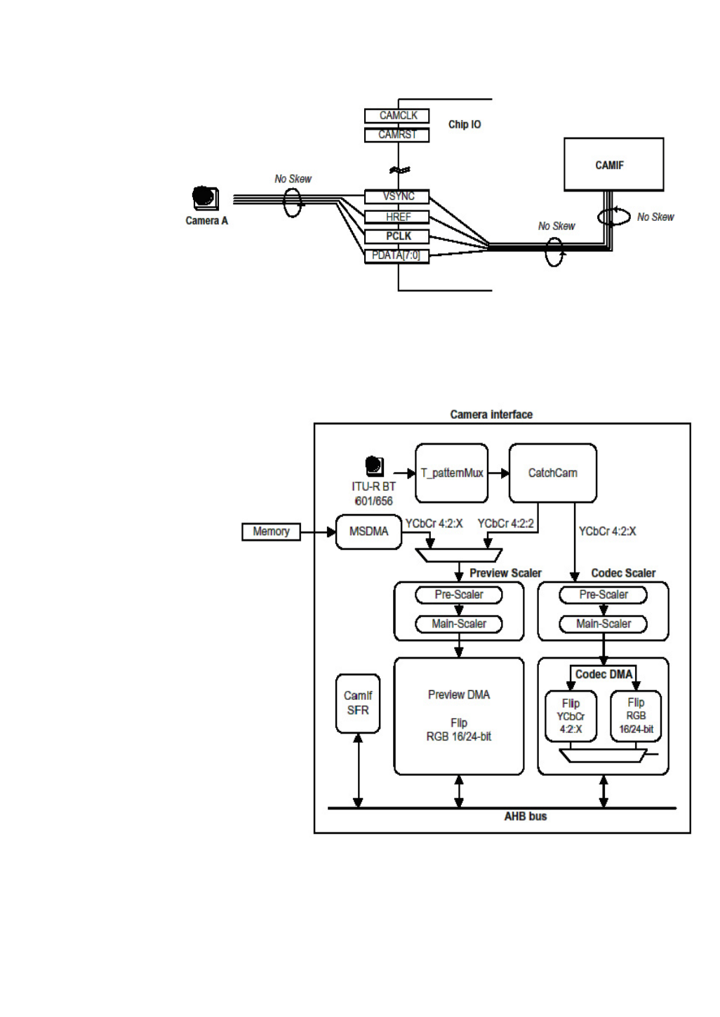
Camera interface The CAMIF (Camera Interface) within the S3C2443X consists of eight parts: pattern
mux, capturing unit, MSDMA (Memory Scaling DMA), preview scaler, codec scaler,
preview DMA, codec DMA, and SFR. The camera interface supports:
ITU R BT-601/656 YCbCr 8-bit standard and Memory
Maximum input size of 4096x4096 pixels (2048x2048 pixels for scaling)
Two scalers:
One is the preview scaler, which is dedicated to generating smaller size images for
previewing. The other one is the codec scaler, which is dedicated to generating codec
useful images like plane type YCbCr 4:2:0 or 4:2:2. Two master DMAs can do mirror
and rotate of the captured image for mobile environments. And test pattern
generation can be used to calibration of input sync signals as HREF, VSYNC. Also,
video sync signals and pixel clock polarity can be inverted in the camera interface
side with using register setting.
Features:
ITU-R BT 601/656 8-bit mode support
DZI (Digital Zoom In) capability
Programmable polarity of video sync signals
Max. 4096 x 4096 pixels input support (non-scaling)
Max. 2048 x 2048 pixels input support for codec scaling and 640 x 480 pixels
input support for preview scaling
Image mirror and rotation (X-axis mirror, Y-axis mirror and 180° rotation)
Preview DMA output image generation (RGB 16/24-bit format)
Codec DMA output image generation (RGB 16/24-bit format or YCbCr
4:2:0/4:2:2 format)
Capture frame control support in codec_path
Scan line offset support in codec_path (YCbCr)
YCbCr 4:2:2 codec image format interleave support
MSDMA supports memory data for preview path input
Image effect
CAMIF supports the following video standards:
ITU-R BT 601 YCbCr 8-bit mode
ITU-R BT 656 YCbCr 8-bit mode
www.digiembedded.com 42
The figure below provides an overview of the CAMIF interface signals.
All camera interface signals should have the same length.
Buffers should be Schmitt-triggered.
Below is the block diagram of the camera interface.
AC97 Controller The AC97 Controller Unit of the S3C2443 supports AC97 revision 2.0 features. AC97
Controller communicates with AC97 Codec using an audio controller link (AC-link).
Controller sends the stereo PCM data to Codec. The external digital-to-analog
converter (DAC) in the Codec then converts the audio sample to an analog audio
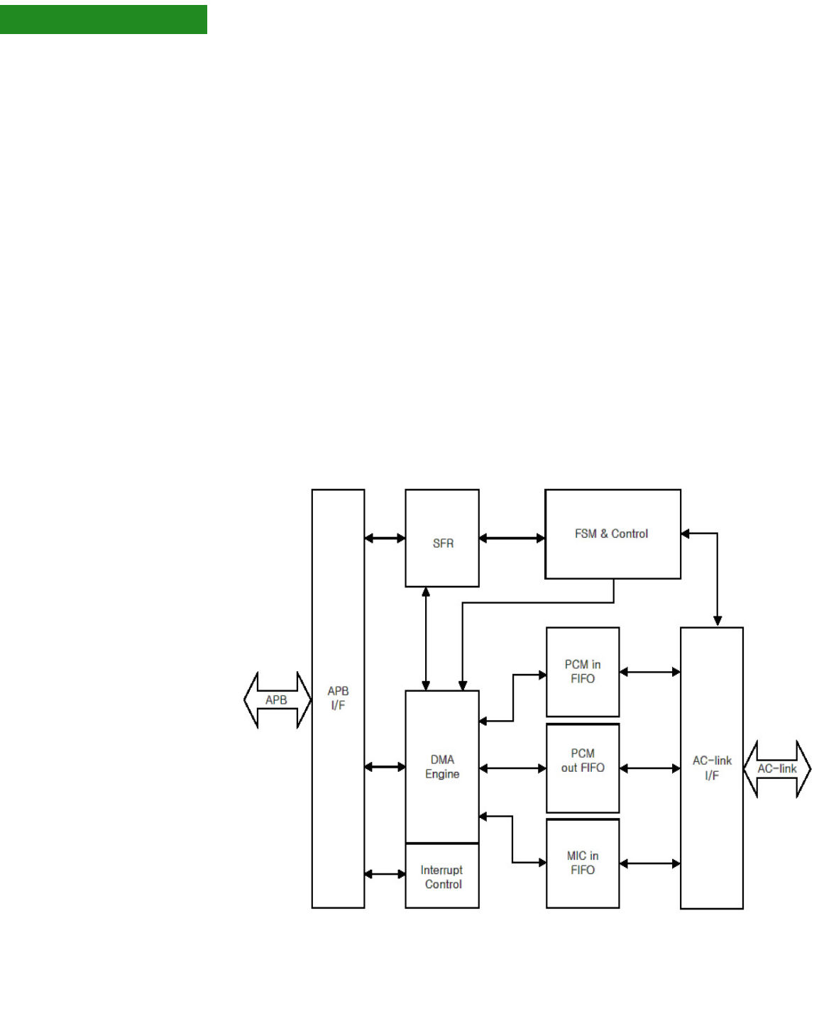
43 ConnectCore 9M 2443 & Wi-9M 2443 Hardware Reference
Chapter 1
waveform. Also, the Controller receives the stereo PCM data and the mono Mic data
from the Codec and then stores them in the memories. This chapter describes the
programming model for the AC97 Controller Unit. The information in this chapter
requires an understanding of the AC97 revision 2.0 specifications.
Note: The AC97 Controller and the IIS Controller must not be used at the same time.
Features:
Independent channels for stereo PCM In, stereo PCM Out, mono MIC In.
DMA-based operation and interrupt based operation.
All of the channels support only 16-bit samples.
Variable sampling rate AC97 Codec interface (48 KHz and below).
16-bit, 16 entry FIFOs per channel
Only Primary CODEC support
The following shows the functional block diagram of the S3C2443 AC97 Controller.
The AC97 signals form the AClink, which is a point-to-point synchronous serial
interconnect that supports full-duplex data transfers. All digital audio streams and
command/status information are communicated over the AC-link.
www.digiembedded.com 44
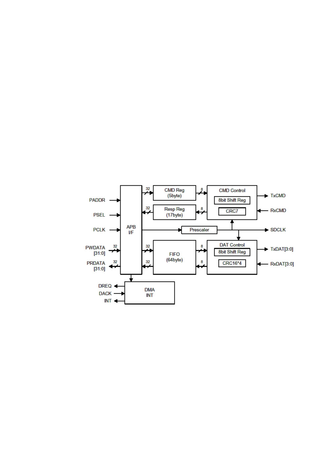
SD host interface The S3C2443 Secure Digital Interface (SDI) can interface for SD memory card, SDIO
device and Multi-Media Card (MMC).
Features:
SD Memory Card Spec. (ver. 1.0) / MMC Spec. (2.11) compatible
SDIO Card Spec (ver. 1.0) compatible
16 words (64 bytes) FIFO (depth 16) for data Tx/Rx
40-bit Command Register
136-bit Response Register
8-bit Prescaler logic (Freq. = System Clock / (P + 1))
Normal, and DMA Data Transfer Mode (byte, halfword, word transfer)
1bit / 4bit (wide bus) Mode & Block / Stream Mode Switch support
DMA burst4 access support (only word transfer)
The following shows the SD host block diagram:
PWM timer The S3C2443 has five 16-bit timers. Timer 0, 1, 2, and 3 have Pulse Width Modulation
(PWM) function. Timer 4 has an internal timer only with no output pins. The timer 0
has a dead-zone generator, which is used with a large current device. The timer 0 and
1 share an 8-bit prescaler, while the timer 2, 3 and 4 share other 8-bit prescaler. Each
timer has a clock divider, which generates 5 different divided signals (1/2, 1/4, 1/8,
1/16, and TCLK). Each timer block receives its own clock signals from the clock
divider, which receives the clock from the corresponding 8-bit prescaler. The 8-bit
prescaler is programmable and divides the PCLK according to the loading value,
which is stored in TCFG0 and TCFG1 registers.
The timer count buffer register (TCNTBn) has an initial value which is loaded into the
down-counter when the timer is enabled. The timer compare buffer register

45 ConnectCore 9M 2443 & Wi-9M 2443 Hardware Reference
Chapter 1
(TCMPBn) has an initial value which is loaded into the compare register to be
compared with the down-counter value. This double buffering feature of TCNTBn and
TCMPBn makes the timer generate a stable output when the frequency and duty ratio
are changed.
Each timer has its own 16-bit down counter, which is driven by the timer clock. When
the down counter reaches zero, the timer interrupt request is generated to inform
the CPU that the timer operation has been completed. When the timer counter
reaches zero, the value of corresponding TCNTBn is automatically loaded into the
down counter to continue the next operation. However, if the timer stops, for
example, by clearing the timer enable bit of TCONn during the timer running mode,
the value of TCNTBn will not be reloaded into the counter.
The value of TCMPBn is used for pulse width modulation (PWM). The timer control
logic changes the output level when the down-counter value matches the value of the
compare register in the timer control logic. Therefore, the compare register
determines the turn-on time (or turn-off time) of a PWM output.
Features:
Five 16-bit timers
Two 8-bit prescalers & Two 4-bit divider
Programmable duty control of output waveform (PWM)
Auto reload mode or one-shot pulse mode
Dead-zone generator
All of the Timer outputs are connected to the system connector.
Clock output At the global pins of the system connector there is a clock signal available
(BCLKOUT0), which is buffered by a clock buffer and can be chosen to be either MPLL
CLK, EPLL CLK, FCLK, HCLK, PCLK or DCLK. The source of this clock signal is the
CLKOUT0 port at the CPU, which can be programmed to different clocks, by the
CLKSEL0 register.
The following table shows the bits [6:4] of the CLKSEL0 register:
CF/ATA The single-slot CF controller consists of 2 parts - PC card controller & ATA controller.
They are multiplexing from or to PAD signals. Users can select either PC card or
True-IDE mode operation. Default mode is PC card mode. The CF controller has a
top level SFR with card power enable bit, output port enable bit & mode select
(True-IDE or PC card) bit.
CLKSELO [6.4] 000 001 010 011 100 101 11x
CLKOUT0 MPLL CLK EPLL CLK FCLK HCLK PCLK DCLK0 Reserved

www.digiembedded.com 46
PC card
controller The PC card controller has 2 half-word (16 bit) write buffers & 4 half-word (16bits)
read buffers.
The PC card controller has 5 word-sized (32 bit) Special Function Registers.
Features:
3 timing configuration registers
Attribute memory
Common memory
I/O interface
1 status & control configuration register
1 interrupt source & mask register
Timing configuration register consists of 3 parts - Setup, Command & Hold
–IDLE, SETUP, COMMAND & HOLD
–Each part of register indicates the operation timing of each state
ATA controller Features:
Compatible with the ATA/ATAPI-6 standar d
Thirty word-sized (32 bit) special function register
One FIFO that is 16 x 32 bit
Internal DMA controller (from ATA device to memory or from memory to ATA
device)
AHB master (DMA controller) supporting 8 burst & word size transfer
The control lines are available on X2.
High-speed MMC The HSMMC (High-speed MMC) / SD-MMC is a combo host for Secure Digital card and
MultiMedia Card. This host is compatible with SD Association's (SDA) Host Standard
Specification.
Interface a system with SD card and MMC card. The performance of this host is very
powerful, supporting 52 MHz clock rate and 8-bit access simultaneously.
Features:
SD Standard Host Spec (ver 1.0) compatible
SD Memory Card Spec (ver 2.1) / MMC Memory card Spec(4.2) compatible
SDIO Card Spec (ver 1.0) compatible
512 bytes FIFO for data Tx/Rx
48-bit Command Register
136-bit Response Register

47 ConnectCore 9M 2443 & Wi-9M 2443 Hardware Reference
Chapter 1
CPU Interface and DMA data transfer mode
1-bit / 4-bit / 8-bit mode switch support
Auto CMD12 support
Suspend / Resume support
Read Wait operation support
Card Interrupt support
CE-ATA mode support
The control lines are available on X2.
High speed SPI The High Speed Serial Peripheral Interface (HS_SPI) can interface the serial data
transfer. HS_SPI has two 8-bit shift registers for transmission and receiving,
respectively. During an SPI transfer, data is simultaneously transmitted (shifted out
serially) and received (shifted in serially). HS_SPI supports the protocols for National
Semiconductor Microwire and Motorola Serial Peripheral Interface.
Features:
Full duplex support
8-bit shift register for TX/RX
8-bit prescale logic
3 clock sources
8-bit/32-bit bus interface
Motorola SPI protocol and National Semiconductor Microwire compliant
Two independent transmit and receive FIFOs (16 samples deep/32-bits wide)
Master-mode and slave-mode
Receive-without-transmit operation
External
address/data bus The external address/data bus supports:
64MB address space per external chip select
Programmable 8/16-bit data bus width
Four external chip selects
Complete programmable access cycles for all memory banks
External wait signals to expand the bus cycle
WLAN connectors In addition to the wired Ethernet interface, the ConnectCore Wi-9M 2443 module
also offers an integrated dual-diversity 802.11a/b/g interface with data rates up to
54 Mbps. Two U.FL antenna connectors are provided on the module. For the Connect
Core Wi-9M 2443, attach the antennas with the U.FL-RP-SMA FEMALE Cable to the
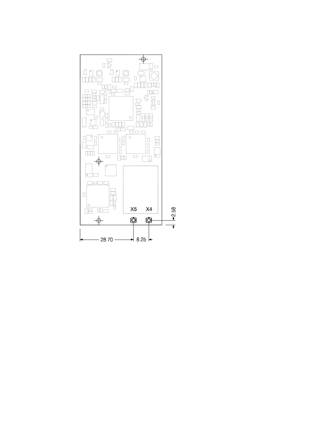
www.digiembedded.com 48
primary connector [X5] and the secondary connector [X4] on the module. You must
use only this cable and antennas to carry on the module.
Note
When disconnecting U.FL connectors, the use of U.FL plug extraction tool
(Hirose P/N U.FL-LP-N-2 or U.FL-LP(V)-N-2) is strongly recommended to
avoid damage to the U.FL connectors on the ConnectCore Wi-9M 2443
module.
To mate U.FL connectors, the mating axes of both connectors must be aligned. The
"click" will confirm fully mated connection. Do not attempt insertion at an extreme
angle.

49 ConnectCore 9M 2443 & Wi-9M 2443 Hardware Reference
Chapter 1
. . . . . . . . . . . . . . . . . . . . . . . . . . . . . . . . . . . . . . . . . . . . . . . . . . . . . . . . . . . . . . . . . . . . . . . . . . . . . . . . . .
LCD controller display features
The LCD controller of the S3C2443 consists of the logic for transferring LCD image
data from a video buffer located in system memory to an external LCD driver. The
LCD controller supports monochrome, 2-bit per pixel (4-level gray scale) or 4-bit per
pixel (16-level gray scale) mode on a monochrome LCD, using a time-based dithering
algorithm and Frame Rate Control (FRC) method and it can be interfaced with a color
LCD panel at 8-bit per pixel (256-level color) and 12-bit per pixel (4096-level color)
for interfacing with STN LCD.
It can support 1-bit per pixel, 2-bit per pixel, 4-bit per pixel, and 8-bit per pixel for
interfacing with the palletized TFT color LCD panel, and 16-bit per pixel and 24-bit
per pixel for non-palletized true-color display. The LCD controller can be
programmed to support different requirements on the screen related to the number
of horizontal and vertical pixels, data line width for the data interface, interface
timing, and refresh rate.
STN LCD
displays
4-bit dual scan, 4-bit single scan, and 8-bit single scan display type
Monochrome, 4 gray levels, and 16 gray levels
256 colors and 4096 colors for color STN LCD panel
Multiple screen size:
–Typical actual screen size: 640 x 480, 320 x 240, 160 x 160, and others
–Maximum virtual screen size is 4Mbytes
–Maximum virtual screen size in 256 color mode: 4096 x 1024, 2048 x 2048,
1024 x 4096, and others
TFT LCD
displays
1, 2, 4 or 8-bpp (bit per pixel) palletized color displays
16, 24-bpp non-palletized true-color displays
Maximum 16M color TFT at 24bit per pixel mode
Multiple screen size:
–Typical actual screen size: 640 x 480, 320 x 240, 160 x 160, and others
–Maximum virtual screen size: 4Mbytes
–Maximum virtual screen size in 64K color mode: 2048 x 1024, and others
2 overlay windows for TFT
Common features The LCD controller has a dedicated DMA that supports fetching image data from
www.digiembedded.com 50
a video buffer located in system memory.
Its features include:
Dedicated interrupt functions (INT_FrSyn and INT_FiCnt)
System memory used as display memory
Multiple Virtual Display Screen (supports hardware horizontal/vertical
scrolling)
Programmable timing control for different display panels
Little and big-endian byte ordering, as well as Windows Embedded CE data
formats
. . . . . . . . . . . . . . . . . . . . . . . . . . . . . . . . . . . . . . . . . . . . . . . . . . . . . . . . . . . . . . . . . . . . . . . . . . . . . . . . . .
Module pinout
System connector
X1 I = Input
O = Output
AI = Analog Input
P = Power
Pin Signal Type Signal name Description
X1-1 GND P GND
X1-2 RSTIN# I RSTIN# Input of a ADM811SARTZ supervisor which
produces PWRGOOD. 10k pull up on module
X1-3 PWRGOOD O PWRGOOD Output of a ADM811SARTZ supervisor. 470R
series resistor on module
X1-4 RSTOUT O RSTOUT# Softw + WDT + RSTIN#
X1-5 TCK I TCK JTAG
X1-6 TMS I TMS JTAG Mode Select
X1-7 TDI I TDI JTAG Data In
X1-8 TDO O TDO JTAG Data Out
X1-12 Conf2 I VD0
GPC8
VD0 can be used for LCD or 24 bit TFT.
On JSCC9M2443 a DIP switch is connected
X1-13 Conf3 I VD1
GPC9
VD1 can be used for LCD or 24 bit TFT.
On JSCC9M2443 a DIP switch is connected
X1-14 Conf4 I VD8
GPD0
VD8 can be used for LCD or 24 bit TFT.
On JSCC9M2443 a DIP switch is connected

51 ConnectCore 9M 2443 & Wi-9M 2443 Hardware Reference
Chapter 1
X1-15 Conf5 I VD9
GPD1
VD9 can be used for LCD or 24 bit TFT.
On JSCC9M2443 a DIP switch is connected
X1-16 Conf6 I VD16
GPD8
VD16 can be used for LCD or 24 bit TFT.
On JSCC9M2443 a DIP switch is connected
X1-17 Conf7 I VD17
GPD9
VD17 can be used for LCD or 24 bit TFT.
On JSCC9M2443 a DIP switch is connected
X1-18 TxDA O TXD0
GPH0
Serial PORT A Transmit Data
X1-19 RxDA I RXD0
GPH1
Serial PORT A Receive Data
X1-20 RTSA# O RTS0#
GPH9
Serial PORT A Request to send
X1-21 CTSA# I CTS0#
GPH8
Serial PORT A Clear to Send
X1-22 I CAMPCLK
GPJ8
Pixel clock driven by the camera processor
X1-23 I CAMHREF
GPJ10
Horizontal sync driven by the camera processor
X1-24 TxDB O TXD2
GPH4
Serial PORT C Transmit Data
X1-25 RxDB I RXD2
GPH5
Serial PORT C Receive Data
X1-26 RTSB# O TXD3
GPH6
RTS2#
Handshake PORT C or PORT D Transmit Data
X1-27 CTSB# I TXD3
GPH7
CTS2#
Handshake PORT C or PORT D Receive Data
X1-28 CAMVSYNC I CAMVSYNC
GPJ9
Frame sync driven by camera processor
X1-29 CAMDATA0 I CAMDATA0
GPJ0
Pixel data driven by the camera processor
X1-30 CAMDATA1 I CAMDATA1
GPJ1
Pixel data driven by the camera processor
X1-31 CAMDATA2 I CAMDATA2
GPJ2
Pixel data driven by the camera processor
X1-32 CAMDATA3 I CAMDATA3
GPJ3
Pixel data driven by the camera processor
Pin Signal Type Signal name Description

www.digiembedded.com 52
X1-33 CAMDATA4 I CAMDATA4
GPJ4
Pixel data driven by the camera processor
X1-34 CAMDATA5 I CAMDATA5
GPJ5
Pixel data driven by the camera processor
X1-35 CAMDATA6 I CAMDATA6
GPJ6
Pixel data driven by the camera processor
X1-36 CAMDATA7 I CAMDATA7
GPJ7
Pixel data driven by the camera processor
X1-37 USB_PWREN# O RSMVAD
GPA14
General purpose output
X1-38 EINT5
VBUSDET
I EINT5
GPF5
General purpose input/output
X1-39 P GND
X1-40 VD2 I/O VD2
GPC10
LCD/TFT Interface
X1-41 VD3 I/O VD3
GPC11
LCD/TFT Interface
X1-42 VD4 I/O VD4
GPC12
LCD/TFT Interface
X1-43 VD5 I/O VD5
GPC13
LCD/TFT Interface
X1-44 VD6 I/O VD6
GPC14
LCD/TFT Interface
X1-45 VD6
GPC14
I/O VD7
GPC15
LCD/TFT Interface
X1-46 EINT18\CF_CD# I/O EINT18
GPG10
LCD/TFT Interface
X1-47 EINT11 I/O EINT11
GPG3
General purpose input / output
X1-48 VD10 I/O VD10
GPD2
LCD/TFT Interface
X1-49 VD11 I/O VD11
GPD3
LCD/TFT Interface
X1-50 VD12 I/O VD12
GPD4
LCD/TFT Interface
X1-51 VD13 I/O VD13
GPD5
LCD/TFT Interface
X1-52 VD14 I/O VD14
GPD6
LCD/TFT Interface
Pin Signal Type Signal name Description
53 ConnectCore 9M 2443 & Wi-9M 2443 Hardware Reference
Chapter 1
X1-53 VD15 I/O VD15
GPD7
LCD/TFT Interface
X1-54 EINT14 I/O EINT14
GPG6
General purpose input / output
X1-55 TCLK0 I/O TCLK0
GPB4
General purpose input / output
X1-56 VD18 I/O VD18
GPD10
LCD/TFT Interface
X1-57 VD19 I/O VD19
GPD11
LCD/TFT Interface
X1-58 VD20 I/O VD20
GPD12
LCD/TFT Interface
X1-59 VD21 I/O VD21
GPD13
LCD/TFT Interface
X1-60 VD22 I/O VD22
GPD14
LCD/TFT Interface
X1-61 VD23 I/O VD23
GPD15
LCD/TFT Interface
X1-62 LCD_PWREN I/O EINT12
GPG4
LCD_PWREN
LCD/TFT Interface
X1-63 VM I/O VM
GPC4
LCD/TFT Interface
X1-64 VFRAME I/O VFRAME
GPC3
LCD/TFT Interface
X1-65 VLINE I/O VLINE
GPC2
LCD/TFT Interface
X1-66 VCLK I/O VCLK
GPC1
LCD/TFT Interface
X1-67 LEND I/O LEND
GPC0
LCD/TFT Interface
X1-68 LCD_LPCOE I/O LCDVF0
GPC5
LCD/TFT Interface
X1-69 LCD_LPCREV I/O LCDVF1
GPC6
LCD/TFT Interface
X1-70 LCD_LPCREVB I/O LCDVF2
GPC7
LCD/TFT Interface
X1-71 TOUT0 I/O TOUT0
GPB0
Timer out
Pin Signal Type Signal name Description

www.digiembedded.com 54
X1-72 TOUT1 I/O TOUT1
GPB1
Timer out
X1-73 NC I/O WLAN_DISABLE# Not connected; reserved for CCW9M
X1-74 NC I/O WLAN_LED# Not connected; reserved for CCW9M
X1-75 SDCLK I/O SD0_CLK
GPE5
AC_BIT_CLK
SD-interface
X1-76 SDCMD I/O SD0_CMD
GPE6
AC_SDI
SD-interface
X1-77 SDDATA0 I/O SD0_DAT[0]
GPE7
AC_SDO
SD-interface
X1-78 SDDATA1 I/O SD0_DAT[1]
GPE8
AC_SYNC
SD-interface
X1-79 GND P GND
X1-80 SDDATA2 I/O SD0_DAT[2]
GPE9
AC_RESET
SD-interface
X1-81 SDDATA3 I/O SD0_DAT[3]
GPE10
SD-interface
X1-82 EINT0 I/O EINT0
GPF0
External interrupts
X1-84 TOUT2 I/O TOUT2
GPB2
Timer out
X1-85 SS1# I/O SS1
GPL14
SPI1 Interface
X1-86 SPIMISO1 I/O SPIMISO1
GPL12
SPI1 Interface
X1-87 SPIMOSI1 I/O SPIMOSI1
GPL11
SPI1 Interface
X1-88 SPICLK1 I/O SPICLK1
GPL10
SPI1 Interface
X1-89 EINT17 I/O EINT17
GPG9
General purpose input / output
X1-90 EINT1\SD_CD# I/O EINT1
GPF1
General purpose input / output
Pin Signal Type Signal name Description
55 ConnectCore 9M 2443 & Wi-9M 2443 Hardware Reference
Chapter 1
X1-92 ROE# I/O ROE# Ext. bus control
X1-93 RWE# I/O RWE# Ext. bus control
X1-94 WAIT# I/O WAIT# Ext. bus control
X1-95 RCS1# I/O RCS1# Chip selects
X1-96 RCS2# I/O RCS2# Chip selects
X1-97 RCS3# I/O RCS3# Chip selects
X1-98 RCS4# I/O RCS4# Chip selects
X1-99 PWREN O PWREN 1.8V core power on-off control
X1-100 BATT_FLT# I BATT_FLT# Battery fault
X1-101 CAMCLKOUT O CAMCLKOUT
GPJ11
Master clock to the camera processor
X1-102 CAMRESET O CAMRESET
GPJ12
Software reset or power down to the camera
processor
X1-103 RBE0# O RBE0# Upper byte / lower byte enable
X1-104 RBE1# O RBE1# Upper byte / lower byte enable
X1-107 SS0# O SS0
GPL13
SPI0 chip select
X1-108 SPIMISO0 I SPIMISO0
GPE1
SPI_Master IN
X1-109 SPIMOSI0 O SPIMOSI0
GPE12
SPI_Master OUT
X1-110 SPICLK0 O SPICLK0
GPE13
SPI0 clock
X1-111 I2CSCL O I2CSCL I2C clock
X1-112 I2CSDA I/O I2CSDA I2C data
X1-113 EINT8
USB_DT/PW
I/O EINT8
GPG0
Not used
X1-114 USBP I/O USBP USB data host1, device
X1-115 USBN I/O USBN USB data host1, device
X1-116 VRTC P VRTC Power for RTC
X1-117 GND P GND
X1-118 +3.3V P +3.3V +3.3V for peripherals
X1-119 VLIO P VLIO Power from Li-Ion battery for core
Pin Signal Type Signal name Description
www.digiembedded.com 56
System connector
X2
X1-120 +3.3V P +3.3V +3.3V for peripherals
Pin Signal Type Signal name Description
Pin Signal Type Signal name Description
X2-1 USBP0 I/O USBP0 USB data host0
X2-2 GND P GND
X2-3 USBN0 I/O USBN0 USB data host 0
X2-4 RADDR0 O RADDR0
GPA0
X2-5 RADDR1 O RADDR1 Address line
X2-6 RADDR2 O RADDR2 Address line
X2-7 RADDR3 O RADDR3 Address line
X2-8 RADDR4 O RADDR4 Address line
X2-9 RADDR5 O RADDR5 Address line
X2-10 RADDR6 O RADDR6 Address line
X2-11 RADDR7 O RADDR7 Address line
X2-12 RADDR8 O RADDR8 Address line
X2-13 RADDR9 O RADDR9 Address line
X2-14 RADDR10 O RADDR10 Address line
X2-15 RADDR11 O RADDR11 Address line
X2-16 RADDR12 O RADDR12 Address line
X2-17 RADDR13 O RADDR13 Address line
X2-18 RADDR14 O RADDR14 Address line
X2-19 RADDR15 O RADDR15 Address line
X2-20 RADDR16 O RADDR16
GPA1
Address line
X2-21 RADDR17 O RADDR17
GPA2
Address line
X2-22 RADDR18 O RADDR18
GPA3
Address line
X2-23 RADDR19 O RADDR19
GPA4
Address line
X2-24 RADDR20 O RADDR20
GPA5
Address line
57 ConnectCore 9M 2443 & Wi-9M 2443 Hardware Reference
Chapter 1
X2-25 RADDR21 O RADDR21
GPA6
Address line
X2-26 RADDR22 O RADDR22
GPA7
Address line
X2-27 RADDR23 O RADDR23
GPA8
Address line
X2-28 RADDR24 O RADDR24
GPA9
Address line
X2-29 RADDR25 O RADDR25
RDATA_OEN
Address line
X2-30 NC - (A26) Pull down on module
X2-31 RxD1 I RXD1
GPH3
Serial PORT B
X2-32 TxD1 O TXD1
GPH2
Serial PORT B
X2-33 CTS1# I CTS1#
GPH10
Serial PORT B
X2-34 RTS1# O RTS1#
GPH11
Serial PORT B
X2-35 reserved
X2-36 XDREQ0# I/O XDREQ0#
GPB10
DMA
X2-37 XDREQ1# I/O XDREQ1#
GPB8
DMA
X2-38 XDACK0# I/O XDACK0#
GPB9
DMA
X2-39 XDACK1# I/O XDACK1#
GPB7
DMA
X2-40 GND P GND
X2-41 AIN4 AI AIN4 A/D converter
X2-42 AIN5 AI AIN5 A/D converter
X2-43 AIN0 AI AIN0 A/D converter
X2-44 AIN1 AI AIN1 A/D converter
X2-45 AIN2 AI AIN2 A/D converter
X2-46 AIN3 AI AIN3 A/D converter
X2-47 AIN6/YM AI AIN6/YM A/D converter or touch interface
X2-48 AIN7/YP AI AIN7/YP A/D converter or touch interface
Pin Signal Type Signal name Description

www.digiembedded.com 58
X2-49 AIN8/XM AI AIN8/XM A/D converter or touch interface
X2-50 AIN9/XP AI AIN9/XP A/D converter or touch interface
X2-51 AVCC P AVCC Analog VCC
X2-52 AGND P AGND Analog GND
X2-53 NC Reserved for CCW9M CPLD_TDI
X2-54 NC Reserved for CCW9M CPLD_TCK
X2-55 NC Reserved for CCW9M CPLD_TMS
X2-56 NC Reserved for CCW9M CPLD_TDO
X2-57 XBREQ# I/O XBREQ#
BPG6
Ext. bus control
X2-58 XBACK# I/O XBACK#
GPB5
Ext. bus control
X2-59 EINT16
USBH0PEN
IEINT16
GPG8
USB0 host power fault if low
X2-60 PME O PME Ethernet controller power management event
X2-61 I2SSDO I/O I2SSDO
GPE4
AC_SDO0
Audio interface
X2-62 I2SSDI I/O I2SSDI
GPE3
AC_SDI0
Audio interface
X2-63 I2SSCDCLK I/O I2SCDCLK
GPE2
AC_BIT_CLK0
Audio interface
X2-64 I2SSCLK I/O I2SSCLK
GPE1
AC_SYNC
Audio interface
X2-65 I2SLRCK I/O I2SLRCK
GPE0
AC_nRESET
Audio interface
X2-66 TPIN I TPIN Ethernet 0 input
X2-67 LEDLNK O LEDLNK Ethernet 0 link/activity LED
X2-68 TPIP I TPIP Ethernet 0 input +
X2-69 LEDSPD O LEDSPD Ethernet 0 speed LED
X2-70 TPON O TPON Ethernet 0 output
X2-71 ETHGPIO2
LED3#
O ETHGPIO2/LED3# Ethernet 0 full duplex LED
Pin Signal Type Signal name Description

59 ConnectCore 9M 2443 & Wi-9M 2443 Hardware Reference
Chapter 1
X2-72 TPOP O TPOP Ethernet 0 output +
X2-73 OE_CF# O OE_CF#
GPA11
Compact Flash interface
X2-74 WE_CF# O WE_CF#
GPA15
Compact Flash interface
X2-75 IREQ_CF# I IREQ_CF#
EINT19
GPG11
Compact Flash interface
X2-76 INPACK_CF# I INPACK_CF#
EINT20
GPG12
Compact Flash interface
X2-77 REG_CF# O REG_CF#
EINT21
GPG13
Compact Flash interface
X2-78 RESET_CF O RESET_CF
EINT22
GPG14
Compact Flash interface
X2-79 PWEN_CF O PWEN_CF
EINT23
GPG15
Compact Flash interface
X2-80 GND P GND
X2-81 RDATA0 I/O RDATA0 Data Bus
X2-82 RDATA1 I/O RDATA1 Data Bus
X2-83 RDATA2 I/O RDATA2 Data Bus
X2-84 RDATA3 I/O RDATA3 Data Bus
X2-85 RDATA4 I/O RDATA4 Data Bus
X2-86 RDATA5 I/O RDATA5 Data Bus
X2-87 RDATA6 I/O RDATA6 Data Bus
X2-88 RDATA7 I/O RDATA7 Data Bus
X2-89 RDATA8 I/O RDATA8 Data Bus
X2-90 RDATA9 I/O RDATA9 Data Bus
X2-91 RDATA10 I/O RDATA10 Data Bus
X2-92 RDATA11 I/O RDATA11 Data Bus
X2-93 RDATA12 I/O RDATA12 Data Bus
X2-94 RDATA13 I/O RDATA13 Data Bus
X2-95 RDATA14 I/O RDATA14 Data Bus
Pin Signal Type Signal name Description

www.digiembedded.com 60
X2-96 RDATA15 I/O RDATA15 Data Bus
X2-97 SD1_DAT0 I/O SD1_DAT0
GPL0
SD card interface 1
X2-98 SD1_DAT1 I/O SD1_DAT1
GPL1
SD card interface 1
X2-99 SD1_DAT2 I/O SD1_DAT2
GPL2
SD card interface 1
X2-100 SD1_DAT3 I/O SD1_DAT3
GPL3
SD card interface 1
X2-101 SD1_DAT4 I/O SD1_DAT4
GPL4
SD card interface 1
X2-102 SD1_DAT5 I/O SD1_DAT5
GPL5
SD card interface 1
X2-103 SD1_DAT6 I/O SD1_DAT6
GPL6
SD card interface 1
X2-104 SD1_DAT7 I/O SD1_DAT7
GPL7
SD card interface 1
X2-105 SD1_CMD I/O SD1_CMD
GPL8
SD card interface 1
X2-106 SD1_CLK I/O SD1_CLK
GPL9
SD card interface 1
X2-107 SD1_WP# I/O SD1_nWP
GPJ15
SD card interface 1
X2-108 SD1_CD# I/O SD1_nCD
GPJ14
SD card interface 1
X2-109 SD1_LED# I/O SD1_LED
GPJ13
SD card interface 1
X2-110 EINT6 I/O EINT6
GPF6
General purpose input / output
X2-111 EINT13 I/O EINT13
GPG5
General purpose input / output
X2-116 CLKOUT1 I/O CLKOUT1
GPH14
Timer output
X2-119 CLKOUT O BCLKOUT0 Buffered clockout0
X2-120 GND P GND
Pin Signal Type Signal name Description

61 ConnectCore 9M 2443 & Wi-9M 2443 Hardware Reference
Chapter 1
. . . . . . . . . . . . . . . . . . . . . . . . . . . . . . . . . . . . . . . . . . . . . . . . . . . . . . . . . . . . . . . . . . . . . . . . . . . . . . . . . .
Configuration pins - CPU
The following configuration pins are hardwired on the module: Default module CPU
configuration.
x = don't care
OM0 is fixed to GND for setting XTAL.
OM4 is fixed to GND for setting NAND.
OM1-3 are depending of the FLASH type.
No pins are available on the module connectors.
MCONF0
(GPF3) MCONF1
(GPF4) MCONF2
(GPM0) MCONF3
(GPF2) MCONF4
(GPH12)
SDRAM-Type 16 MB00xxx
32 MB01xxx
64 MB10xxx
128 MB11xxx
SDRAM-CL 2 xx00x
3 xx01x
4 xx10x
5 xx11x
CPU 400 MHzxxxx0
533 MHzxxxx1

. . . . .
www.ConnectCore 9M 2443 & Wi-9M 2443 Hardware Reference.com 62
About the Development Board
CHAPTER 2
The ConnectCore 9M 2443 Development Board supports the ConnectCore 9M 2443
and ConnectCore Wi-9M 2443 module. This chapter describes the different
components of the development board, which provides the following main features:
What’s on the
development
board?
RJ-45 Ethernet Connector
Connectors for Digi 802.3af PoE application board (sold separately)
1 x UART RS232 with status LEDs and SUB-D 9-pin connector
1 x UART MEI (RS232/RS4xx) with status LEDs and SUB-D 9-pin connectors
2 x UART with TTL levels
USB Host Connector
USB Device Connector
SPI, I2C headers
LCD Application Connector with Touch Screen Interface
VGA interface
2 x User LEDs (green)
2 x User Keys
1 x Debug LED
Screw-flange connector for GPIO
Peripheral application header 0
–Including access to 16-bit data /10-bit address bus signals
Connectors with 1:1 copies of module pins
Eight-position configuration DIP switch
Flexible 9-30VDC power supply
Test points and current measurement options (+3.3V & 5V)
3V coin cell battery
JTAG connector
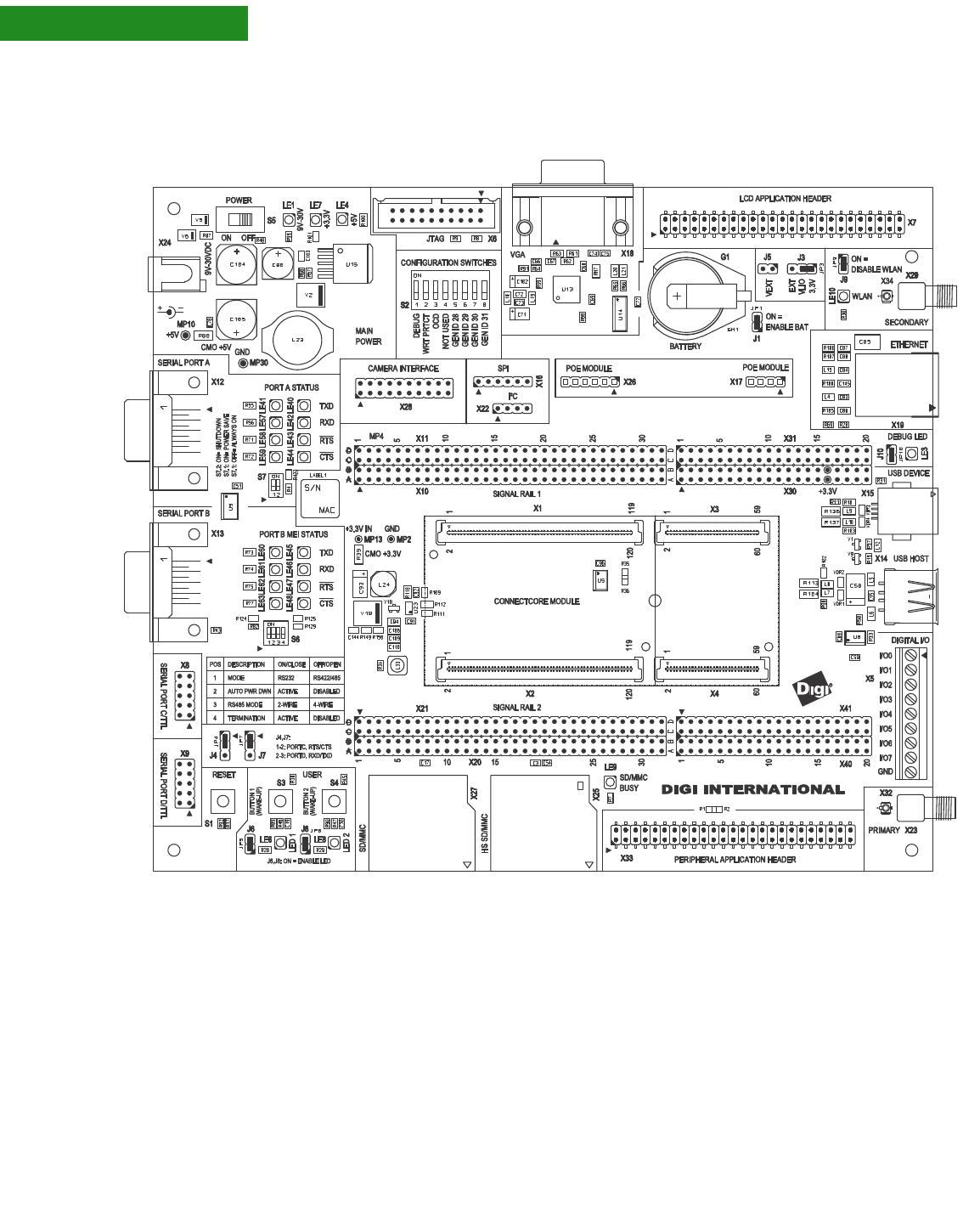
63 ConnectCore 9M 2443 & Wi-9M 2443 Hardware Reference
Chapter 2
The development
board
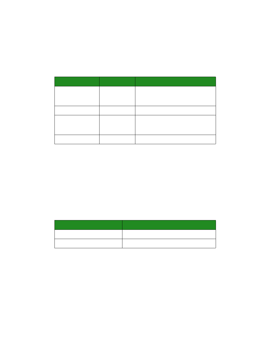
. . . . .
www.ConnectCore 9M 2443 & Wi-9M 2443 Hardware Reference.com 64
. . . . . . . . . . . . . . . . . . . . . . . . . . . . . . . . . . . . . . . . . . . . . . . . . . . . . . . . . . . . . . . . . . . . . . . . . . . . . . . . . .
User interface
The ConnectCore 9M 2443 development board implements two user buttons and two
user LEDs in addition to those provided on the module. The user LEDs on the
development board can be enabled or disabled by correctly setting jumper J5 and
J6. The table below shows which S3C22443 GPIO is available for implementing the
user interface.
Both push-buttons can also be used for wake-up functions.
Power
management User buttons can also be used as a wake-up event for power management modes.
The user LEDs on the development board can be enabled or disabled by correctly
setting J5/J6.
. . . . . . . . . . . . . . . . . . . . . . . . . . . . . . . . . . . . . . . . . . . . . . . . . . . . . . . . . . . . . . . . . . . . . . . . . . . . . . . . . .
General information
The integrated on-chip functions of the module are outlined below.
Power supply ConnectCore 9M 2443 Development Board is powered by either the main 9-
30VDC power supply or by the PoE (IEEE 802.3af) module near to the Ethernet
connector.
Both power supply sources can be switched off through one power switch.
From the varying input voltage (9-30VDC), a stable base power supply is
created on the ConnectCore 9M 2443 development board. The 3.3VDC power
supply is provided to the module, where other power supplies can be
generated.
Signal name GPIO used Comments
USER_BUTTON1 GPF0 100 Ohm serial resistors should be used to
avoid conflicts with the CPU functions when
the buttons are pushed.
USER_LED1# GPL11 Jumper JP5 as to be set.
USER_BUTTON2 GPF1 100 Ohm serial resistors are used to avoid
conflicts with the CPU functions when the
buttons are pushed.
USER_LED2# GPL10 Jumper JP6 as to be set.
Signal name GPIO used
USER_LED_1 GPL11
USER_LED_2 GPL10

65 ConnectCore 9M 2443 & Wi-9M 2443 Hardware Reference
Chapter 2
3.3VDC power
controller - VLIO
The ConnectCore 9M 2443 module supports another external power source:
VLIO. This power source normally comes from a battery and is used in Mobile
application for generating the S3C2443 core voltage. On the ConnectCore 9M
2443 development board, VLIO is selectable by jumper setting onboard
+3.3VDC, or external VLIO.
Power LEDs Two power LEDs are available on the development board, and indicate:
–presence of 9-30VDC power supply,
–presence of +5V, or
–presence of 3.3VDC power supply.
All power LEDs are red.
Coin cell for RTC A 3.0V coin cell should be used on the ConnectCore 9M 2443 development
board for powering the RTC unit on the module.
Current
measuring option
Measuring the current on the development board allows evaluation of power
needed for various board designs.
A current measuring option is implemented by adding a weak resistor in a
series with the power supply that needs to be measured.
Current measurement values might be performed for 3.3VDC, VLIO and VRTC.
Coin cell battery voltage can also be monitored by adding a jumper between
the coincell and the VRTC power supply on the ConnectCore 9M 2443 module.
Reset A push-button allows manual reset by connecting RSTIN# to ground. The reset
controller is located on the ConnectCore 9M 2443 module.
JTAG interface The module JTAG interface is supported through a 20-pin Multi-ICE JTAG
connector, which is located on the ConnectCore 9M 2443 development board.
This connector supports RTCK signal (optional).
TRST# signal has a 2.2K pull-down resistor on module. This means a debugger
with push-pull output at TRST# is needed and open drain is not working.
I²C interface The ConnectCore 9M 2443 module provides access to one I²C channel. 4k7 pull-
ups resistors are used on the module for these signals.
I²C signals are accessible on the 1:1 expansion connectors and on the
dedicated I²C header.
PoE connectors The POE connectors support the PoE Application Module.

. . . . .
www.ConnectCore 9M 2443 & Wi-9M 2443 Hardware Reference.com 66
Peripheral
application
connector
The Peripheral application connector supports the JumpStart Application
Modules.
LCD Application
Kit Connector
The LCD Application Kit Connector supports the JumpStart LCD modules.
VGA interface A standard VGA Interface is provided to support an external monitor.
UARTs The ConnectCore 9M 2443 development board is supporting the 4 UARTs
available on the ConnectCore 9M 2443 module. Detailed usage, of each UART is
described in the following chapters.
UART A - console The ConnectCore 9M 2443 UART A signals are used as the standard console.
This UART supports TXD, RXD and CTS#, RTS# handshake lines.
UART A signals are available on RS232 levels. This connector is a DSUB9 male
which will connect to the host via null modem cable.
UART A is providing status LEDs on TXD, RXD, RTS# and CTS# handshake signals.
UART A line drivers can be disabled if required.
UART B - UART /
MEI
The ConnectCore 9M 2443 UART B signals are full-function UART, providing
access to TXD, RXD and CTS#, RTS# handshake signals.
UART B signals are available on RS232 levels. This connector is a DSUB9 male
which will connect to the host via null modem cable.
UART B is providing status LEDs on TXD, RXD, RTS#, CTS#.
UART B is also the interface supporting the Digi MEI interface (RS422/RS485).
UART B line drivers can be disabled if required.
UART C - TTL
interface
The ConnectCore 9M 2443 UART C signals provide access to TXD, RXD and CTS#,
RTS# (if UART D is not used, else TXD, RXD only).
UART C signals are available on TTL levels. Connector is a 2x5-pin 2.54mm
header compatible with TTL2RS232 adapter (P/N: FS-276).
UART D - TTL
interface
The ConnectCore 9M 2443 UART D signals provide access to TXD and RXD signals
(if UART C handshake is not used).
UART D signals are available on TTL levels. This connector is a 2x5-pin 2.54mm
header compatible with TTL2RS232 adapter (P/N: FS-276).

67 ConnectCore 9M 2443 & Wi-9M 2443 Hardware Reference
Chapter 2
SPI interface(s) The ConnectCore 9M 2443 development board provides access to ConnectCore
9M 2443 module's SPI interfaces SPI0 and SPI1.
HS SPI0 signals are available on the dedicated SPI 6-pin header.
HS SPI0 and SPI1 are also available on the 1:1 extension connectors.
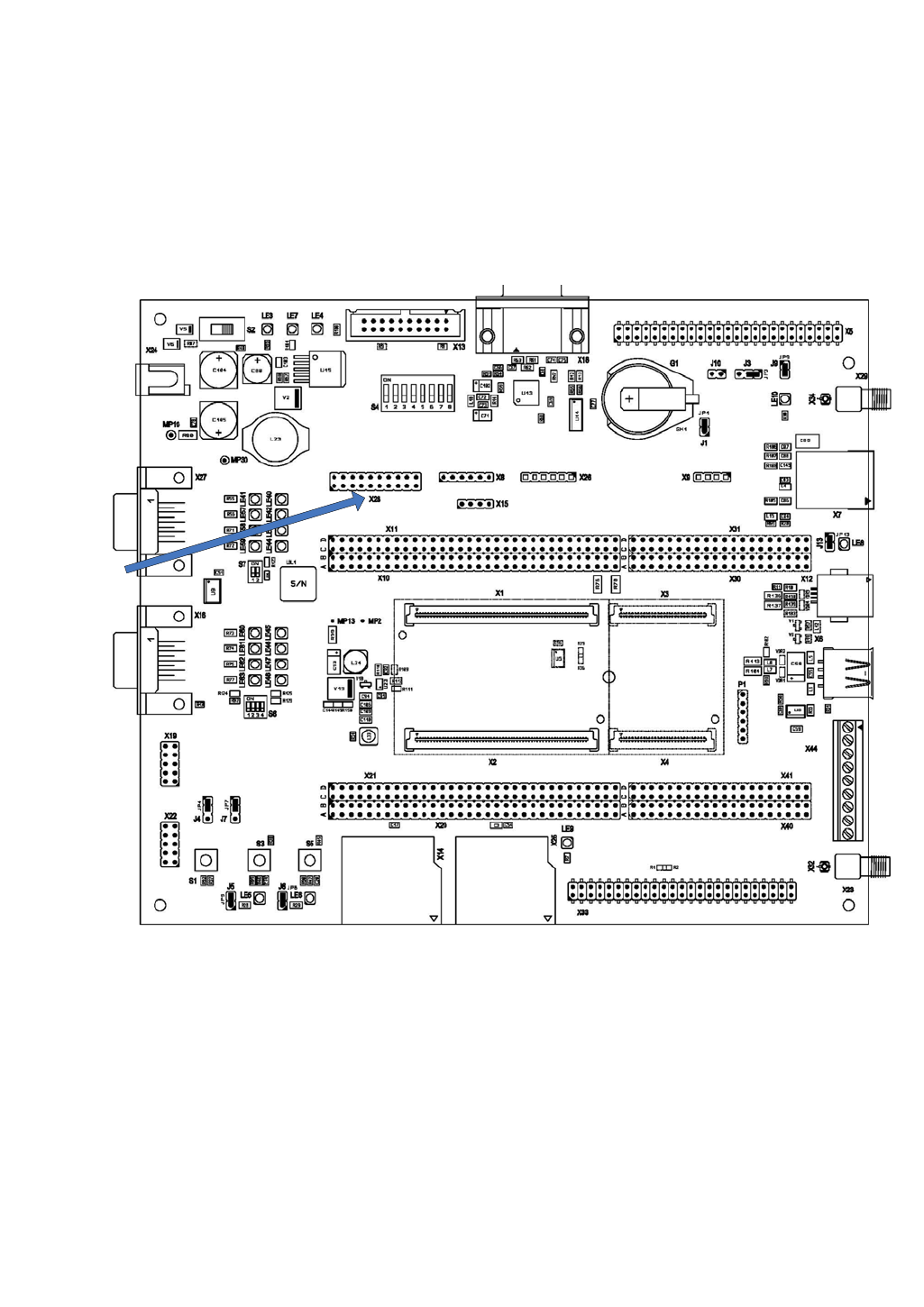
. . . . .
www.ConnectCore 9M 2443 & Wi-9M 2443 Hardware Reference.com 68
. . . . . . . . . . . . . . . . . . . . . . . . . . . . . . . . . . . . . . . . . . . . . . . . . . . . . . . . . . . . . . . . . . . . . . . . . . . . . . . . . .
Camera interface
The camera interface supports ITU R BT-601/656 YCbCr 8-bit standard and Memory.
Maximum input size is 4096x4096 pixels (2048x2048 pixels for scaling).Two scalers
exist. One is the preview scaler, which is dedicated to generate smaller size images
for preview. The other one is the codec scaler, which is dedicated to generate codec
useful images like plane type YCbCr 4:2:0 or 4:2:2.
The Digi Multimedia Application Kit (Digi P/N CC-ACC-MMK-2443) provides a camera
sensor reference design. Please contact your distributor or Digi sales office for
details.
Camera
interface,
X28
69 ConnectCore 9M 2443 & Wi-9M 2443 Hardware Reference
Chapter 2
. . . . . . . . . . . . . . . . . . . . . . . . . . . . . . . . . . . . . . . . . . . . . . . . . . . . . . . . . . . . . . . . . . . . . . . . . . . . . . . . . .
Switches and push-buttons
Reset control, S1 The reset push-button S1, resets the module. On the module, RSTOUT# and
PWRGOOD are produced for peripherals. A push-button allows manual reset by
connecting RSTIN# to ground. The reset controller is located on the module.
Power switch, S2 The development board has an ON/OFF switch S2. The power switch S2 can switch
both 9V-30V input power supply and 12V coming out of the PoE module. However, if
a power plug is connected to the DC power jack, the PoE module is disabled. User
pushbuttons, S3 and S5.
Configuration
switches, S4
Power switch, S2
Serial
port A
switch,
S7
Serial
port B
switch,
S6
Reset button, S1 User
button 1,
S3
User
button 2,
S5
. . . . .
www.ConnectCore 9M 2443 & Wi-9M 2443 Hardware Reference.com 70
Use the user push-buttons to interact with the applications running on the module.
Use these module signals to implement the push-buttons:
Legend for multi-
pin switches Switches S4, S6, and S7 are multi-pin switches. In the description tables for these
switches, the pin is designated as S[switch number].[pin number]. For example, pin
1 in switch 2 is specified as S4.1.
Module
configuration
switches, S4
Use S2 to configure the module:
Serial port B MEI
configuration
switches
Use S6 to configure the line interface for serial port B MEI.
Signal name Switch
(pushbutton GPIO used
USER_PUSH_BUTTON_1 S3 GPF0
USER_PUSH_BUTTON_2 S5 GPF6
Dip-
switch
position
Usage
1 DEBUGEN#
2 Reserved
3OCD_EN
4Reserved
5 SW_CONF4
Switch
pin Function Comments
S6.1 On = RS232 transceiver enabled
RS422/RS485 transceiver disabled
Off= RS232 transceiver disabled
RS422/RS485 transceivers enabled
S6.2 On = Auto Power Down enabled
Off = Auto Power Down disabled
Auto Power Down is not supported on
this board. This signal is only accessible
to permit the user to completely disable
the MEI interface for using signals for
other purposes. To disable the MEI
interface go in RS232 mode (S6.1 = ON)
and activate the Auto Power Down
feature (S6.2 = ON). Be sure that no
cable is connected to connector X3.
S6.3 On = 2 wire interface (RS422/RS485)
Off = 4 wire interface (RS422)
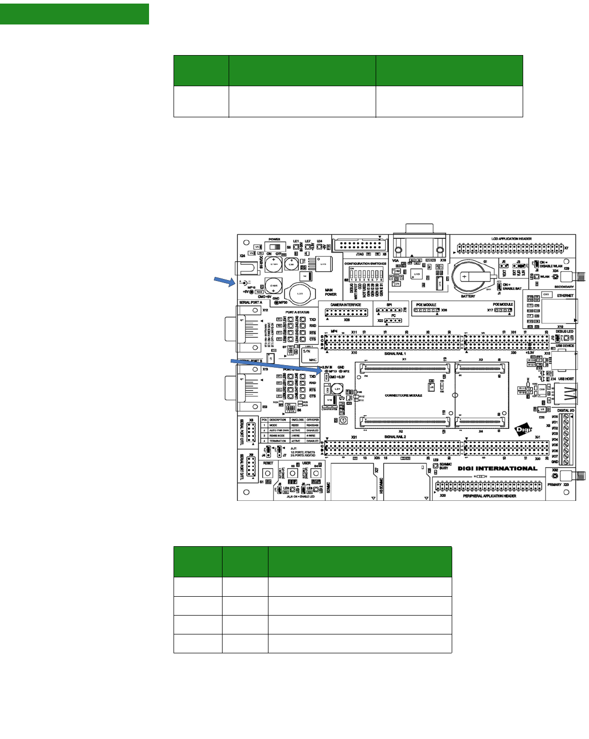
71 ConnectCore 9M 2443 & Wi-9M 2443 Hardware Reference
Chapter 2
. . . . . . . . . . . . . . . . . . . . . . . . . . . . . . . . . . . . . . . . . . . . . . . . . . . . . . . . . . . . . . . . . . . . . . . . . . . . . . . . . .
Test points
The development board provides four test points that can be identified by board
label or test point number.
Numbers and
description
S6.4 On = Terminator on
Off = No termination
Switch
pin Function Comments
Test points
+5V and GND,
MPIO / MP30
Test points
+3.3V and
GND, MP13 /
MP2
Test
point Label Source / comment
MP10 +5V DC/DC regulator (U15) with 9-30VDC input
MP30 GND Common ground
MP13 +3.3V DC/DC regulator (U23) with 5VDC input
MP2 GND Common ground
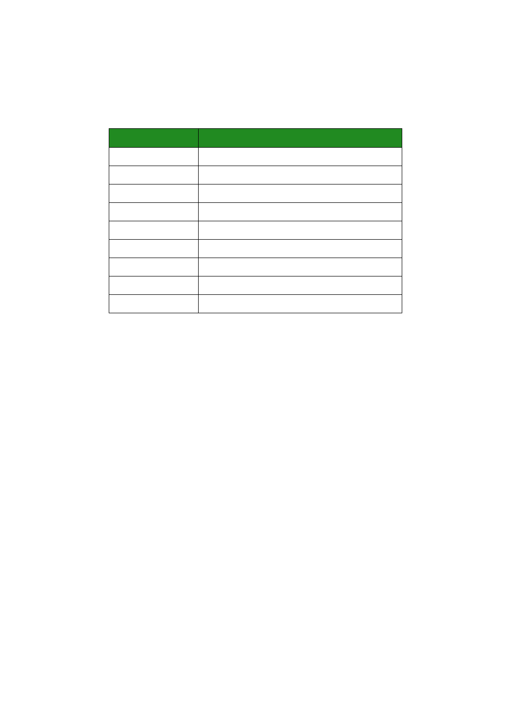
. . . . .
www.ConnectCore 9M 2443 & Wi-9M 2443 Hardware Reference.com 72
Factory default interface configuration for development
. . . . . . . . . . . . . . . . . . . . . . . . . . . . . . . . . . . . . . . . . . . . . . . . . . . . . . . . . . . . . . . . . . . . . . . . . . . . . . . . . .
board
These interfaces are enabled as shown per factory default configuration:
Interface Factory default status
LCD VGA Enabled
I2C Enabled
I2C user-driven I/Os Enabled
EIA-232 Serial Port A Enabled
EIA-485 Serial Port A Disabled
EIA-232 Serial Port B Enabled
TTL Serial Port C Disabled
TTL Serial Port D Disabled
SPI Serial Port B Disabled
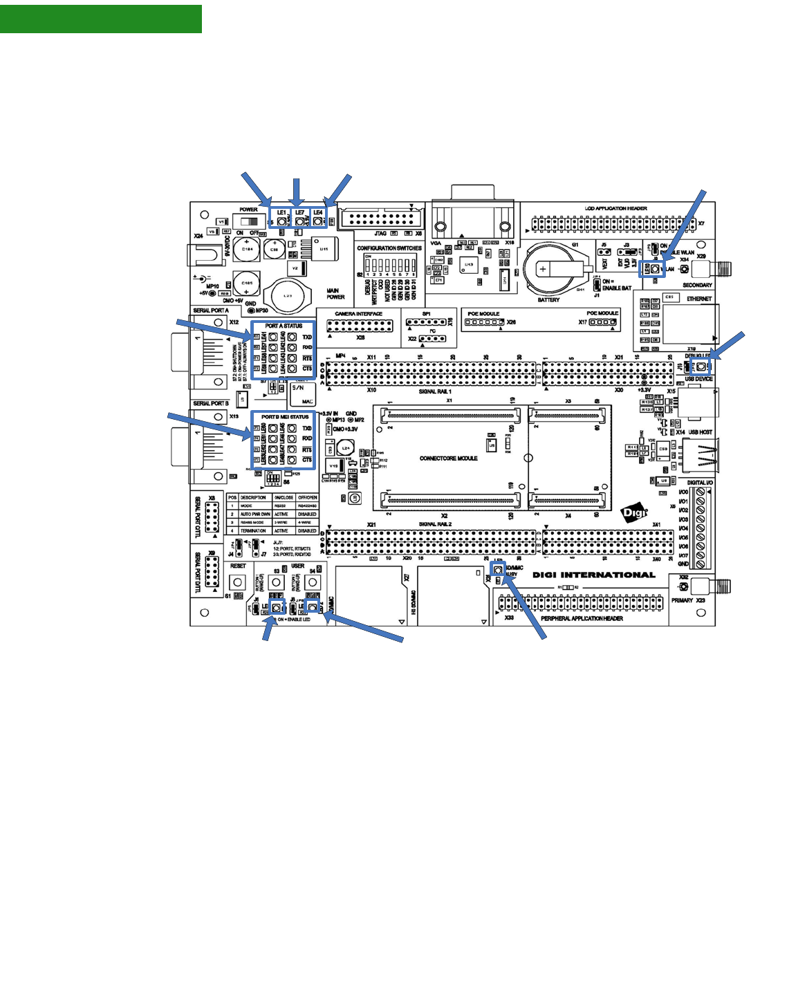
73 ConnectCore 9M 2443 & Wi-9M 2443 Hardware Reference
Chapter 2
. . . . . . . . . . . . . . . . . . . . . . . . . . . . . . . . . . . . . . . . . . . . . . . . . . . . . . . . . . . . . . . . . . . . . . . . . . . . . . . . . .
LEDs
WLAN, LE10 LED indicating WLAN activity.
Power LEDs,
LE1, LE4, and
LE7
The power LEDs are all red. These power supplies must be present and cannot be
switched.
LE1 ON indicates +9VDC / +30VDC power is present
LE4 ON indicates +5VDC power is present
LE7 ON indicates +3.3VDC power is present
User LED1,LE5 SD/MMC activity LED, LE9
Serial
port A
status
LEDs
Serial
port B
status
LEDs
Debug
LED
LE3
Wireless
LAN
activity
LED,
LE10
Power
LED
+5V,
LE4
Power LED
3-3V, LE7
Power LED 9-30V, LEI
User LED2, LE6
Power LED
9-30V, LEI
. . . . .
www.ConnectCore 9M 2443 & Wi-9M 2443 Hardware Reference.com 74
User LEDs, LE5
and LE6 The user LEDs are controlled through applications running on the modules if J6 and
J8 are set. Use these module signals to implement LEDs:
Serial status
LEDs The development board has two sets of serial port LEDs - eight for serial port A and
eight for serial port B. The LEDs are connected to the TTL side of the RS232 or
RS422/485 transceivers.
Green means corresponding signal is high
Red means corresponding signal is low
Signal name LED GPIO used
USER_LED1# LE5 GPL11
USER_LED2# LED6 GPL10
Serial port A
(R232), X27
Serial port B,
(MEI), X16
Serial port C,
TTL, X19
Serial port D,
TTL, X22
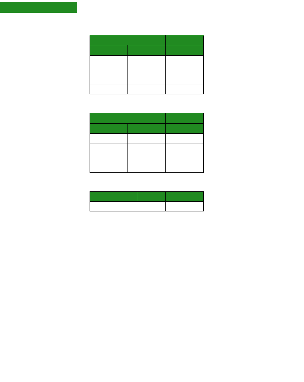
75 ConnectCore 9M 2443 & Wi-9M 2443 Hardware Reference
Chapter 2
Status LEDs
Serial port A
Status LEDs
Serial port B
Debug, LE3
LED reference Function
RED GREEN
LE59 LE44 CTS0#/GPH8
LE58 LE43 RTS0#/GPH9
LE57 LE42 RXD0/GPH1
LE41 LE40 TXD0/GPH0
LED reference Function
RED GREEN
LE63 LE48 CTS1#/GPH10
LE62 LE47 RTS1#/GPH11
LE61 LE46 RXD1/GPH3
LE60 LE45 TXD01GPH2
Signal name LED GPIO used
DEBUG_LED LE8 GPB2/TOUT2
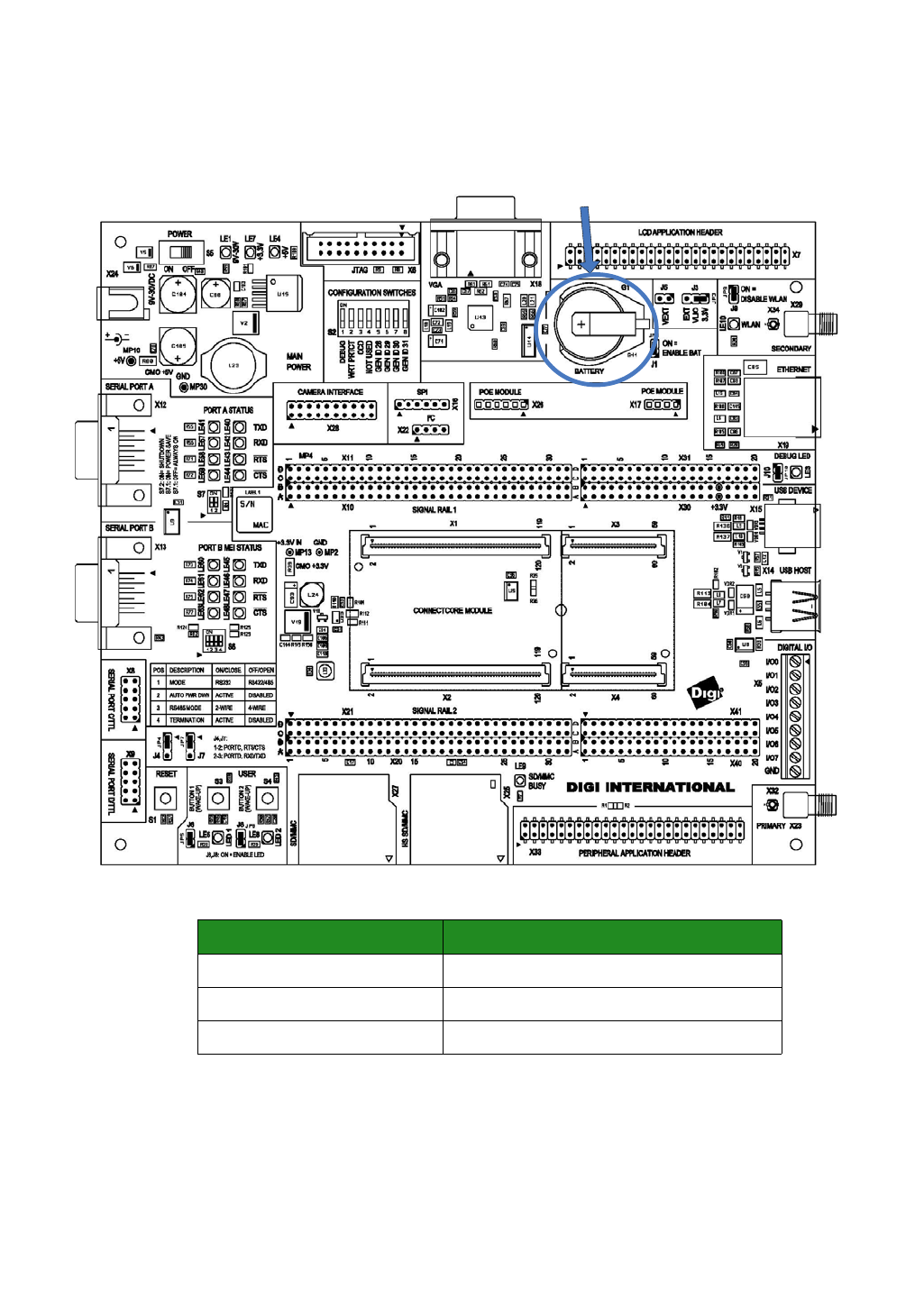
. . . . .
www.ConnectCore 9M 2443 & Wi-9M 2443 Hardware Reference.com 76
. . . . . . . . . . . . . . . . . . . . . . . . . . . . . . . . . . . . . . . . . . . . . . . . . . . . . . . . . . . . . . . . . . . . . . . . . . . . . . . . . .
Battery and battery holder
The development board provides a battery to back up the module integrated RTC
while the main power is disconnected.
The Jumper J1 controls whatever battery power is available. For more information
see the section, “Jumpers” on page 103 of this document.
Battery and battery holder,
G1
Battery holder Battery
Coin-Cell Holder for CR2032 Battery Lithium coin cell
SMD 200mAh
Keystone 1061TR Renata CR2032
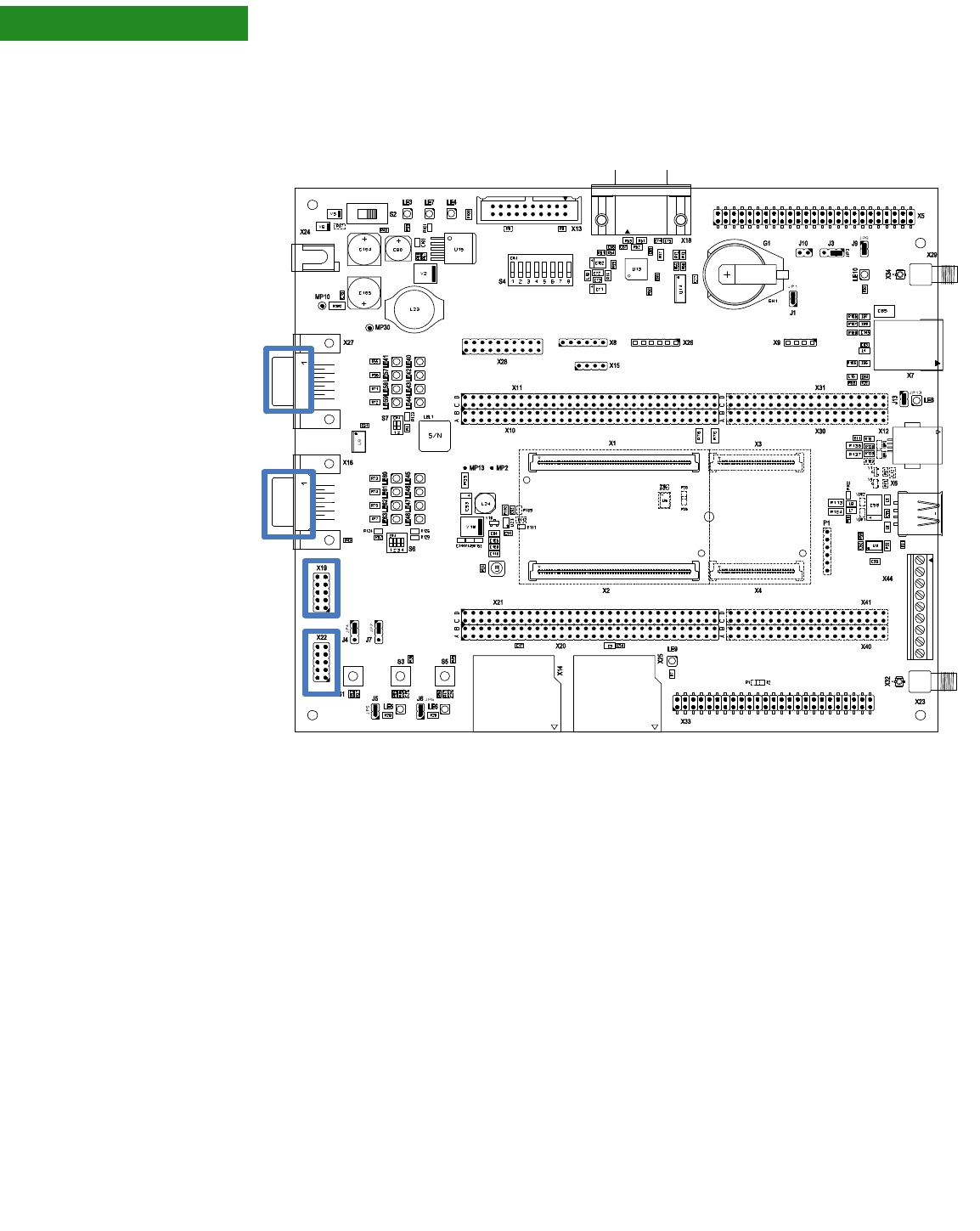
77 ConnectCore 9M 2443 & Wi-9M 2443 Hardware Reference
Chapter 2
. . . . . . . . . . . . . . . . . . . . . . . . . . . . . . . . . . . . . . . . . . . . . . . . . . . . . . . . . . . . . . . . . . . . . . . . . . . . . . . . . .
Serial UART ports
Serial port A,
RS232, X27 The serial (UART) port A connector, X27, is a DSUB9 male connector and is also used
as the standard console port. This asynchronous serial port is DTE and requires a
null-modem cable to connect to a computer serial port.
The serial port A interface corresponds to S3C2443 UART 0. The line driver is
enabled or disabled using S7.2.
Refer to page 68 for information about switch settings.
Serial port A
(R232), X27
Serial port B,
(MEI), X16
Serial port C,
TTL, X19
Serial port D,
TTL, X22
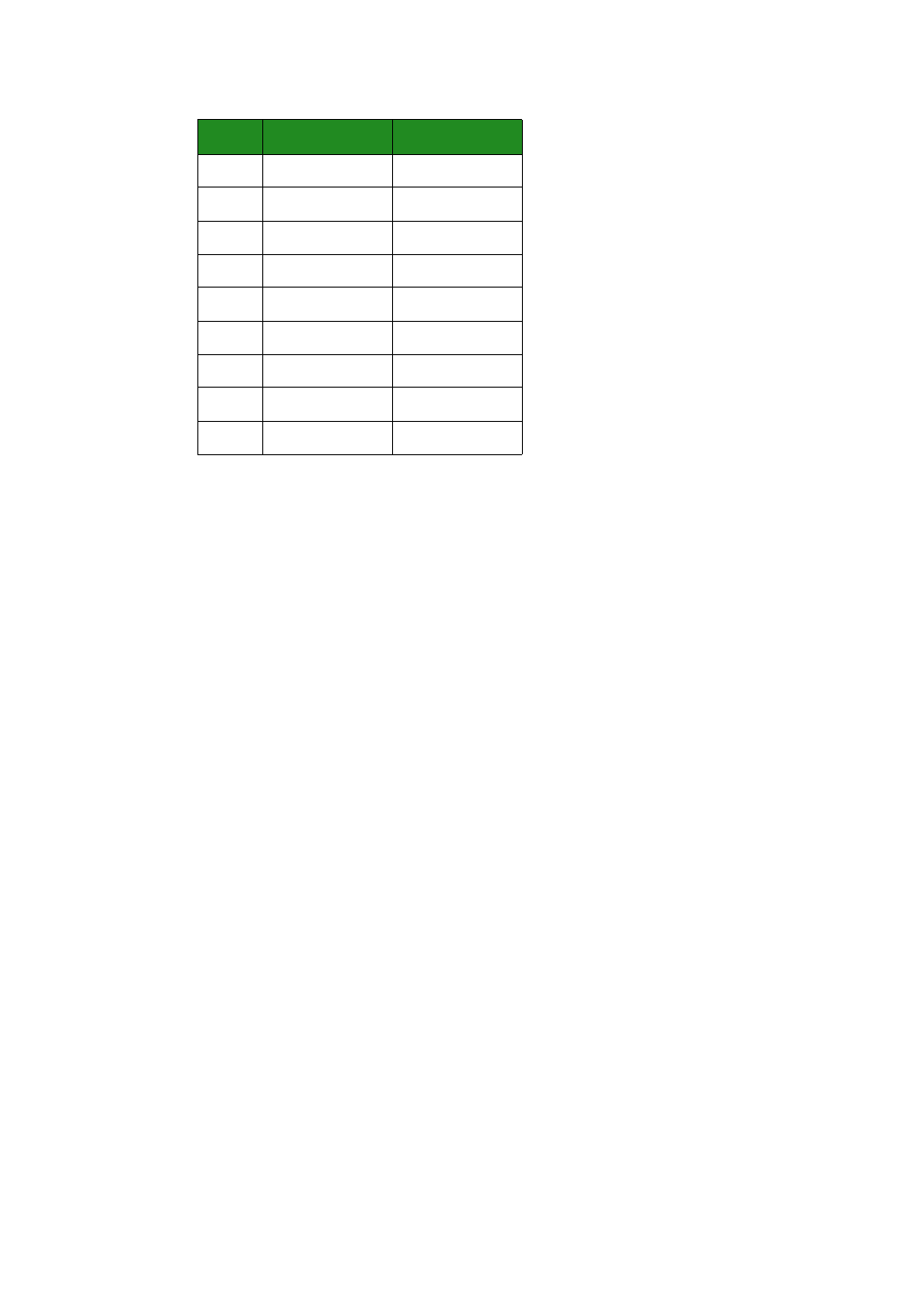
. . . . .
www.ConnectCore 9M 2443 & Wi-9M 2443 Hardware Reference.com 78
Serial port A pins are allocated as shown below:
By default, serial A signals are configured to their respective GPIO signals. It is the
responsibility of the driver to configure them properly.
Pin Function Defaults to
1NC -
2 RXD GPH1
3 TXD GPH0
4NC -
5 GND -
6NC -
7RTS# GPH9
8CTS# GPH8
9NC -
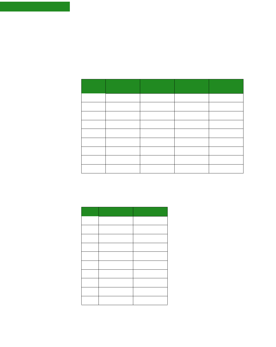
79 ConnectCore 9M 2443 & Wi-9M 2443 Hardware Reference
Chapter 2
Serial port B,
MEI interface,
X16
The serial (UART) port B connector X16 is a DSUB9 male connector. This
asynchronous serial port is DTE and requires a null modem cable to connect to a
computer serial port.
The serial port B MEI (multiple electrical interface) interface corresponds to
S3C2443 UART port B. The line drivers are configured using switch S6.
Note that all port B pins are allocated as shown:
By default serial B signals are configured to their respective GPIO signals. It is the
responsibility of the driver to configure them properly.
Serial port C,
TTL interface,
X19
Pin RS232
function RS232
default RS485
function RS485
default
1CTS-n/a
2 RXD GPH3 RX+ GPH3
3 TXD GPH2 TX+ GPH2
4RTS-n/a
5 GND - GND -
6RX-n/a
7 RTS# GPH11 RTS+ GPIO11
8 CTS# GPH10 CTS+ GPH10
9TX-n/a
Pin Function Defaults to
1NC
2NC
3 RXD2 GPH5
4 RTS2#/TXD3 GPH6
5 TXD2 GPH4
6 CTS2#/RXD3 GPH7
7NC
8NC
9GND
10 +3.3V
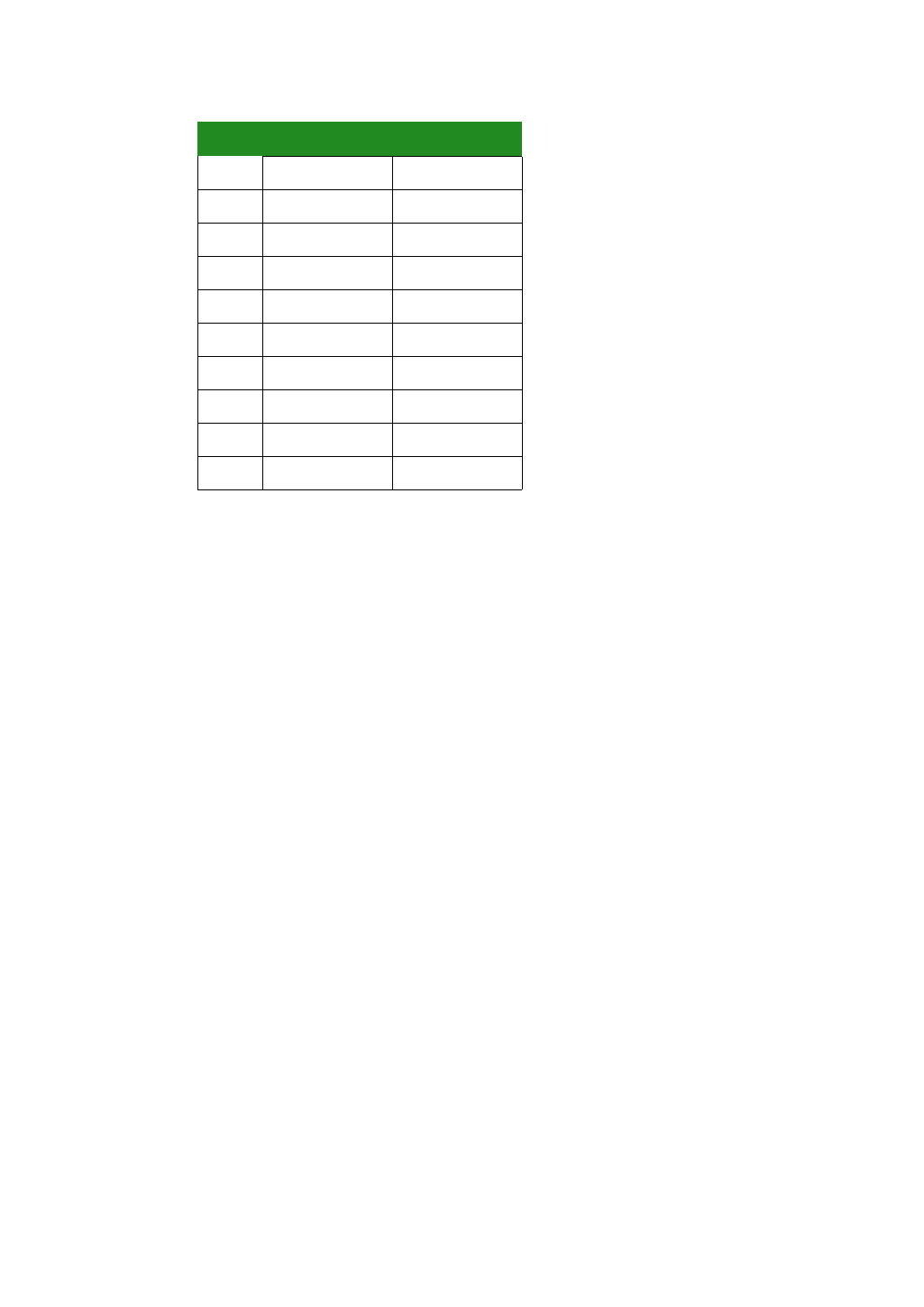
. . . . .
www.ConnectCore 9M 2443 & Wi-9M 2443 Hardware Reference.com 80
Serial port D,
TTL interface,
X22 Pin Function Defaults to
1NC
2NC
3CTS2#/RXD3GPH7
4NC
5RTS2#/TXD3GPH6
6NC
7NC
8NC
9 GND
10 +3.3V
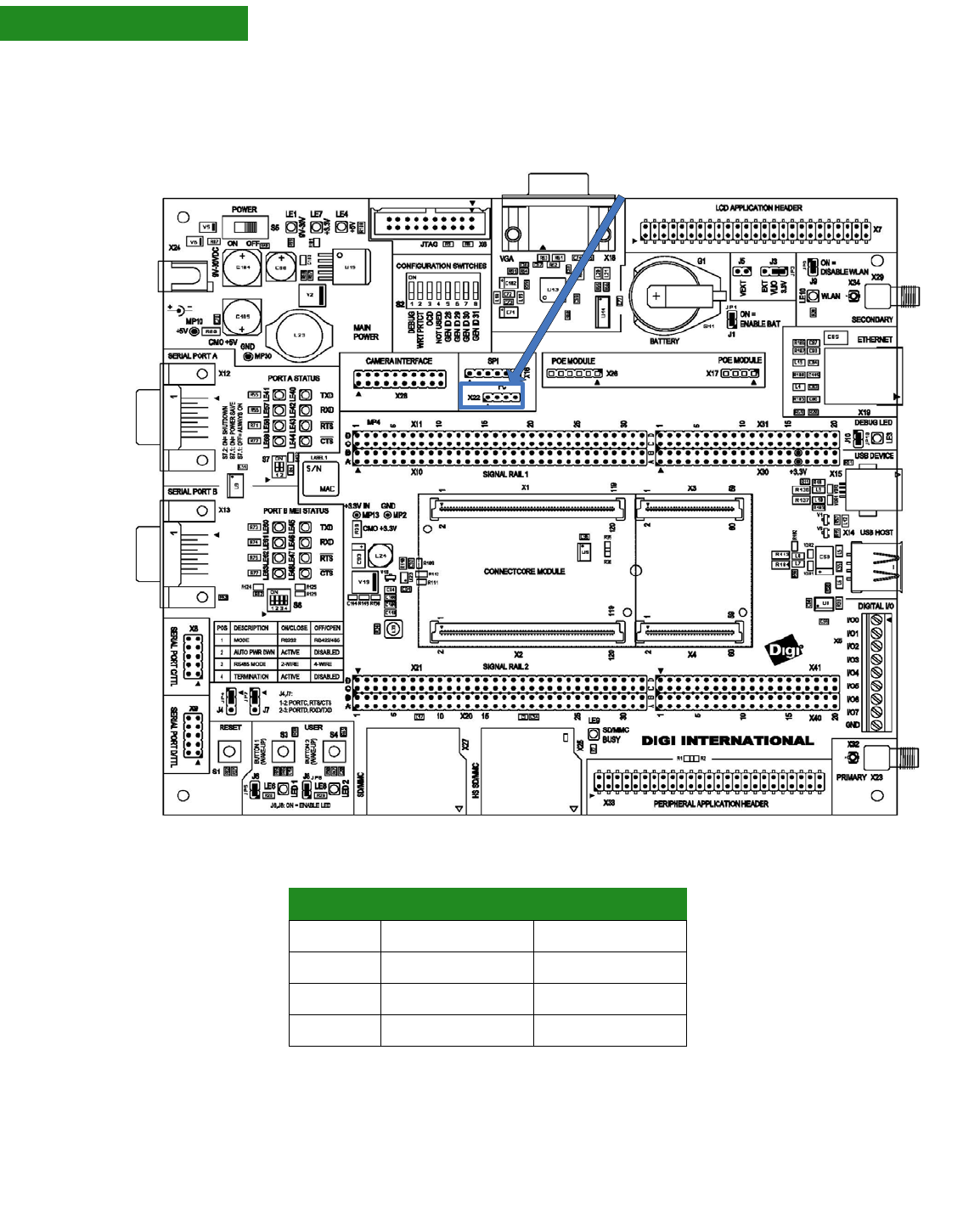
81 ConnectCore 9M 2443 & Wi-9M 2443 Hardware Reference
Chapter 2
. . . . . . . . . . . . . . . . . . . . . . . . . . . . . . . . . . . . . . . . . . . . . . . . . . . . . . . . . . . . . . . . . . . . . . . . . . . . . . . . . .
I2C interface
I2C connector,
X22 The table below provides the pinout of the I2C header.
See page 91 for information about I/O expander I2C device on the development
board.
I2C header, X22
Pin Function Comment
1 I2C_SDA GPE15
2+3.3V
3I2C_SCL GPE14
4GND
. . . . .
www.ConnectCore 9M 2443 & Wi-9M 2443 Hardware Reference.com 82
. . . . . . . . . . . . . . . . . . . . . . . . . . . . . . . . . . . . . . . . . . . . . . . . . . . . . . . . . . . . . . . . . . . . . . . . . . . . . . . . . .
SPI interface
SPI header, X8
83 ConnectCore 9M 2443 & Wi-9M 2443 Hardware Reference
Chapter 2
X8-SPI connector The following table provides the pinout of the SPI header:
Pin Function Comment
1+3.3V
2 SPIMOSI0 GPE12 or High speed SPI Master Out Slave In
3 SPI_MISO0 GPE12 or High speed SPI Master In Slave Out
4 SPI_CLK0 GPE12 or High speed SPI clock
5 SS0# GPE13 or High speed SPI Chip Select
6GND
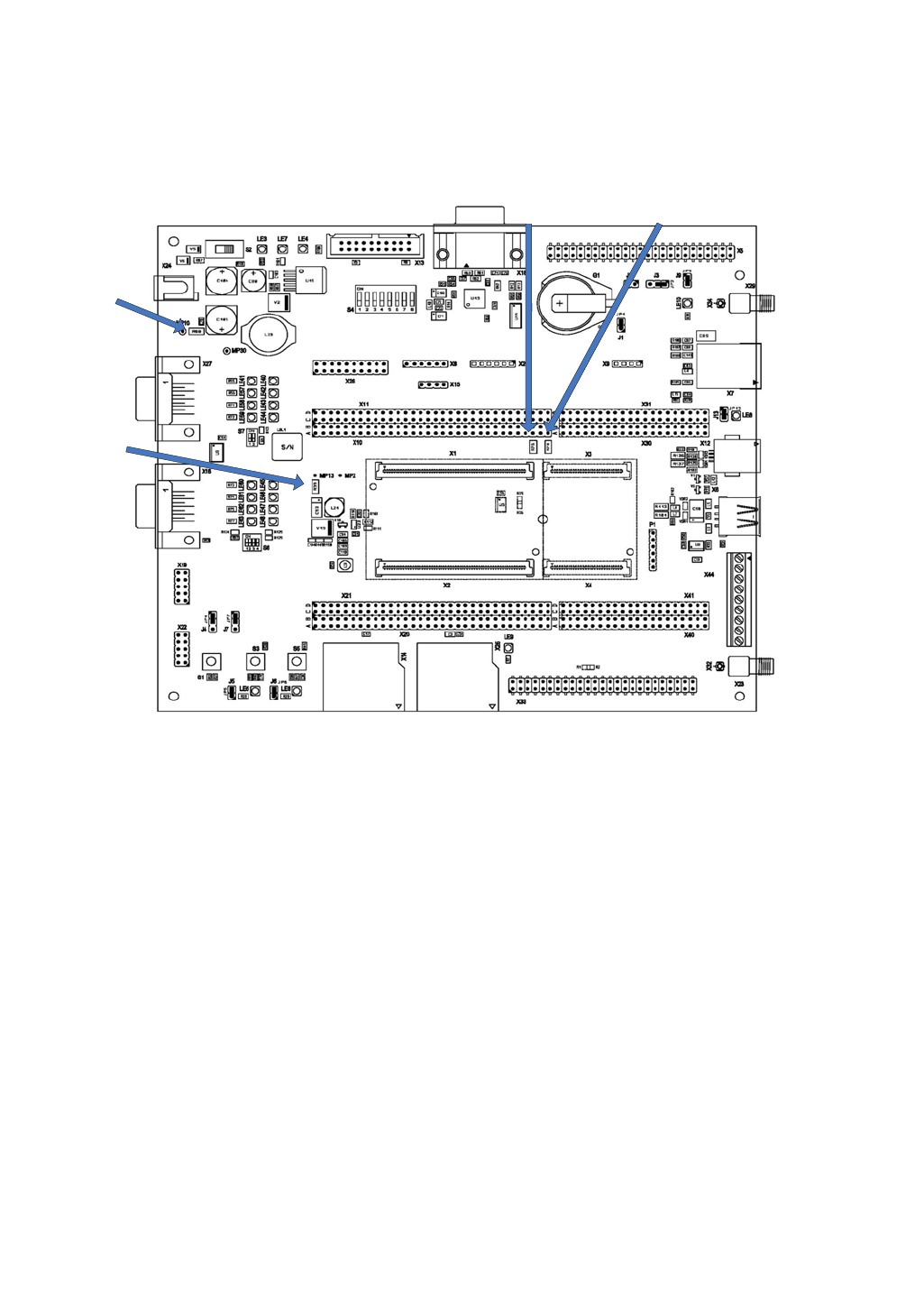
. . . . .
www.ConnectCore 9M 2443 & Wi-9M 2443 Hardware Reference.com 84
. . . . . . . . . . . . . . . . . . . . . . . . . . . . . . . . . . . . . . . . . . . . . . . . . . . . . . . . . . . . . . . . . . . . . . . . . . . . . . . . . .
Current Measurement Option
Measurement
options The Current Measurement Option uses 0.025R ohm series resistors to measure the
current. The ConnectCore 9M 2443 Development board can measure:
the +5V current used by the development board and module (through R80),
the +3.3V current into the +3.3V regulator U23 (through R39),
the +3.3V current into the module (through R70), and
the VLIO current into the module (through R76).
Current
Measurement
Option (CMO)
+5V development
board and
module, R80
Current
Measurement
Option (CMO)
+3.3V
development
board and
module, R39
Current Measurement Option
(CMO) +3.3V, R70
VLIO, R76

85 ConnectCore 9M 2443 & Wi-9M 2443 Hardware Reference
Chapter 2
How the CMO
works To measure the load current used on different power supplies, measure DC voltage
across the sense (CMO) resistor. The value of the resistor is 0.025R ± 1%.
Calculate the current using this equation: I = U/R
where
I = current in Ampere
U = measured voltage in Volt
R = 0.025 Ohm
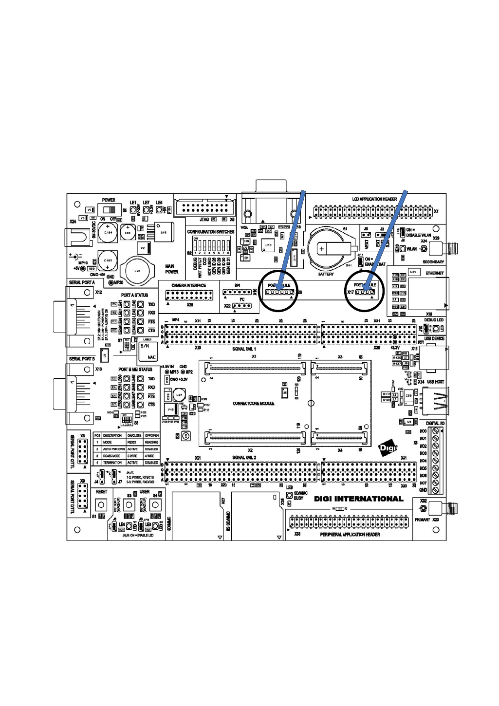
. . . . .
www.ConnectCore 9M 2443 & Wi-9M 2443 Hardware Reference.com 86
. . . . . . . . . . . . . . . . . . . . . . . . . . . . . . . . . . . . . . . . . . . . . . . . . . . . . . . . . . . . . . . . . . . . . . . . . . . . . . . . . .
PoE module connectors - IEEE802.3af
The development board has two PoE module connectors, X9 and X26. The PoE
module is an optional accessory item that can be plugged on the development board
through the two connectors:
X26, output connector: Provides the output power supply from the PoE module.
X17, input connector: Provides access to the PoE signals coming from the
Ethernet interface.
PoE header, X26 PoE header, X17
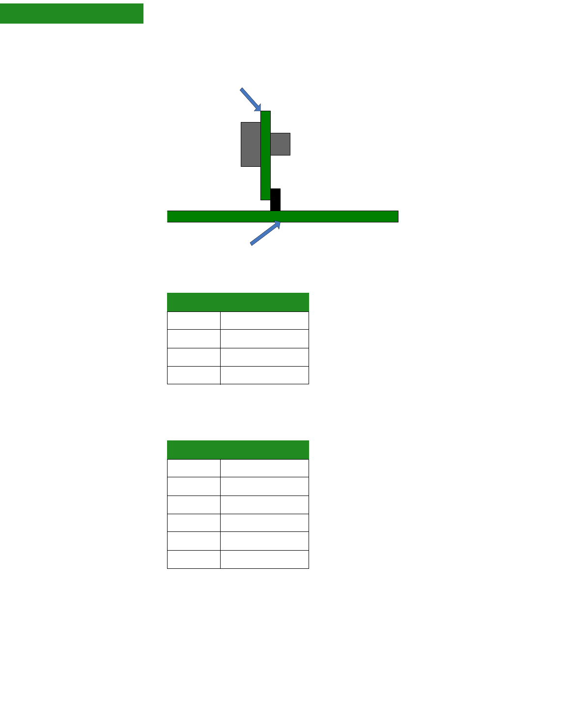
87 ConnectCore 9M 2443 & Wi-9M 2443 Hardware Reference
Chapter 2
The PoE module Plug in the PoE module at a right angle to the development board, as shown in this
drawing:
PoE connector
(power in), X17
PoE connector
(power out), X26
POE_GND The development board provides access to POE_GND allowing it to be turned off
when power is provided through Power Jack X26.9 and X26.5.
PoE module
Jump Start
development board
Pin Function
1POE_TX_CT
2POE_RX_CT
3 POE_RJ45_4/5
4 POE_RJ45_7/8
Pin Function
1+12V
2+12V
3GND
4GND
5 POE_GND
6 POE_GND
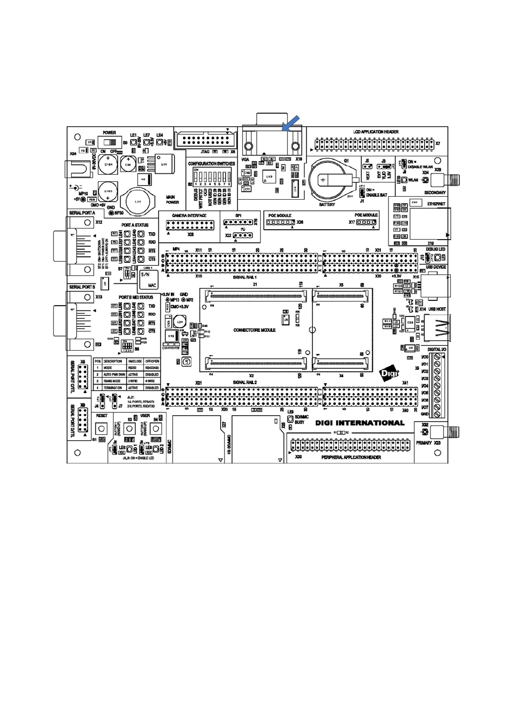
. . . . .
www.ConnectCore 9M 2443 & Wi-9M 2443 Hardware Reference.com 88
. . . . . . . . . . . . . . . . . . . . . . . . . . . . . . . . . . . . . . . . . . . . . . . . . . . . . . . . . . . . . . . . . . . . . . . . . . . . . . . . . .
VGA connector
VGA connector,
X18 The VGA connector is a 15-pin female connector, labeled X18.
VGA connector, X18
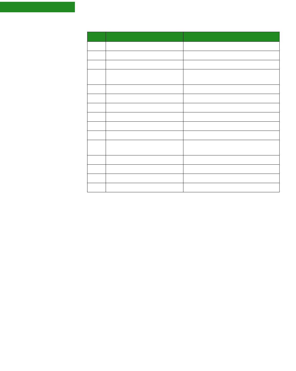
89 ConnectCore 9M 2443 & Wi-9M 2443 Hardware Reference
Chapter 2
X18 pin
assignment Pin Signal Comment
1 VGA_RED
2 VGA_GREEN
3 VGA_BLUE
4 NC (Monitor ID2) Monitor ID2 is not implemented on the
development board
5 GND
6 VGA_GND (RED_RETURN)
7 VGA_GND (GREEN_RETURN)
8 VGA_GND (BLUE_RETURN)
9NC
10 GND (SYNC_RETURN)
11 NC (Monitor ID0) Monitor ID0 is not implemented on the
development board
12 NC
13 HSYNC
14 VSYNC
15 NC
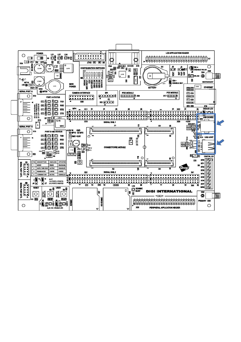
. . . . .
www.ConnectCore 9M 2443 & Wi-9M 2443 Hardware Reference.com 90
. . . . . . . . . . . . . . . . . . . . . . . . . . . . . . . . . . . . . . . . . . . . . . . . . . . . . . . . . . . . . . . . . . . . . . . . . . . . . . . . . .
USB connectors
USB device
connector, X15 This standard type B receptacle provides access to the module USB device
interface. The module supports low, full, and high speed USB2.0 connectivity.
USB host
connector, X14 This standard type A receptacle provides access to the module USB host interface.
The module supports USB 2.0 device connectivity using low and full speed data
rates.
USB host
connector,
X14
USB device
connector,
X15
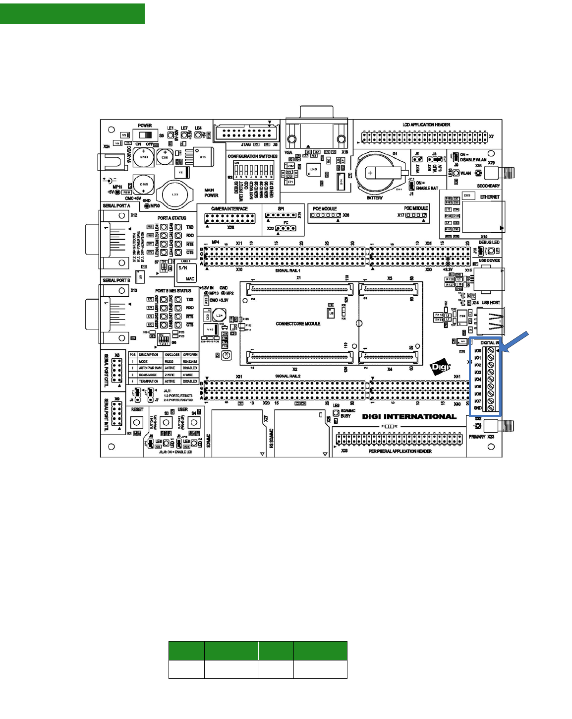
91 ConnectCore 9M 2443 & Wi-9M 2443 Hardware Reference
Chapter 2
. . . . . . . . . . . . . . . . . . . . . . . . . . . . . . . . . . . . . . . . . . . . . . . . . . . . . . . . . . . . . . . . . . . . . . . . . . . . . . . . . .
Digital I/O
Manufacturer part number: BlockMaster MTS0900T
I2C digital I/O
expansion, X44 The development board provides a 3.81mm (1.50”) green terminal block, X44, for
additional digital I/Os. The I2C I/O port chip is on-chip ESD-protected, 5V tolerant,
and provides an open drain interrupt output.
The I/O expander is a Philips PCA9554D at I2C address 0x20 (bits A7..A1), or
0x40/0x41 if expressed in 8-bit format including the R/W bit at the end (bits A7..A1
+ R/W bit)."
The pins are allocated as shown below:
Digital I/O
connector, X44
Pin Function Pin Function
1IO_0 6IO_5
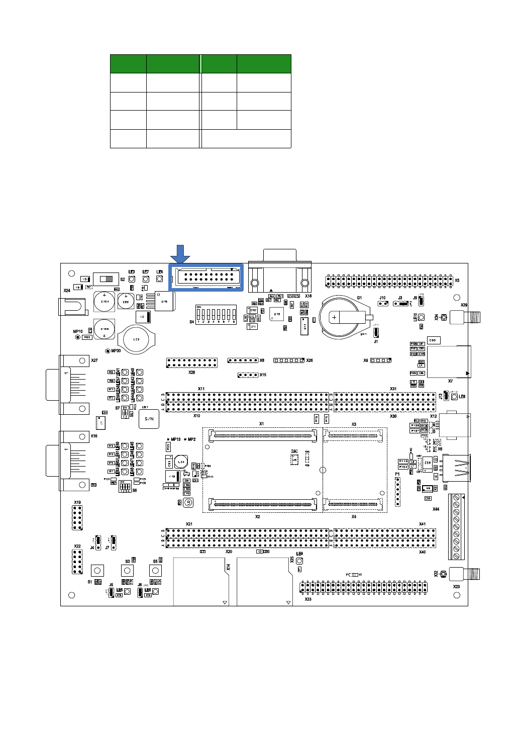
. . . . .
www.ConnectCore 9M 2443 & Wi-9M 2443 Hardware Reference.com 92
. . . . . . . . . . . . . . . . . . . . . . . . . . . . . . . . . . . . . . . . . . . . . . . . . . . . . . . . . . . . . . . . . . . . . . . . . . . . . . . . . .
JTAG interface
2IO_1 7IO_6
3IO_2 8IO_7
4 IO_3 9 GND
5IO_4
Pin Function Pin Function
JTAG connector, X13
R76 R70
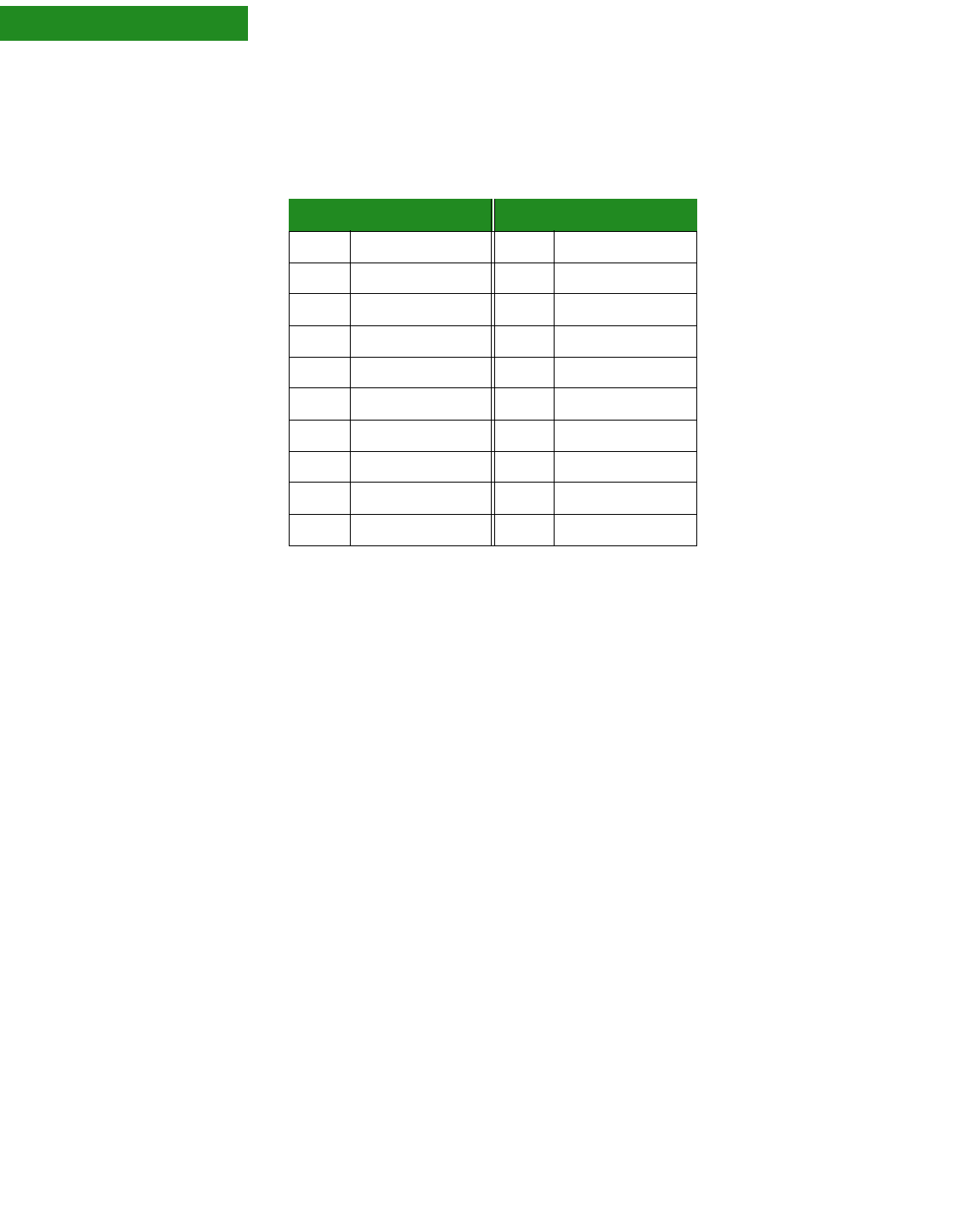
93 ConnectCore 9M 2443 & Wi-9M 2443 Hardware Reference
Chapter 2
Standard JTAG
ARM connector,
X13
The standard JTAG ARM connector is a 20-pin header and can be used to connect
development tools such as Digi JTAG Link, ARM Multi-ICE, Abatron BDI2000 and
others.
Pin Signal Pin Signal
1+3.3V 2+3.3V
3TRST# 4GND
5 TDI 6 GND
7TMS 8GND
9 TCK 10 GND
11 RTCK (optional) 12 GND
13 TDO 14 GND
15 SRESET# 16 GND
17 No connect 18 GND
19 No connect 20 GND
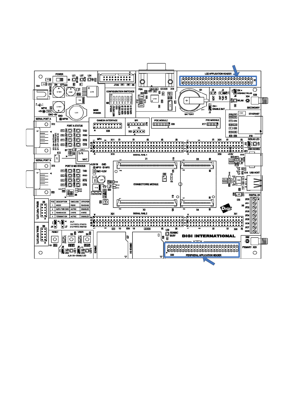
. . . . .
www.ConnectCore 9M 2443 & Wi-9M 2443 Hardware Reference.com 94
. . . . . . . . . . . . . . . . . . . . . . . . . . . . . . . . . . . . . . . . . . . . . . . . . . . . . . . . . . . . . . . . . . . . . . . . . . . . . . . . . .
Peripheral (extension) headers
The development board provides two, 2x25-pin, 0.10” (2.54mm) pitch headers for
supporting application-specific daughter cards/expansion boards:
X5, LCD application header. Provides access to the LCD signals and SPI signals
for touch controller purposes. Use with a Digi-provided application kit or
attach your own application board.
X33, Peripheral application header. Provides access to an 8/16 bit data bus, 8-
bit address bus, and control signals (such as CE#, WE#), as well as I2C and
power. Using these signals, you can connect Digi-specific extension modules or
your own daughter card to the module’s address/data bus.
Peripheral application
header, X33
LCD application header, X5
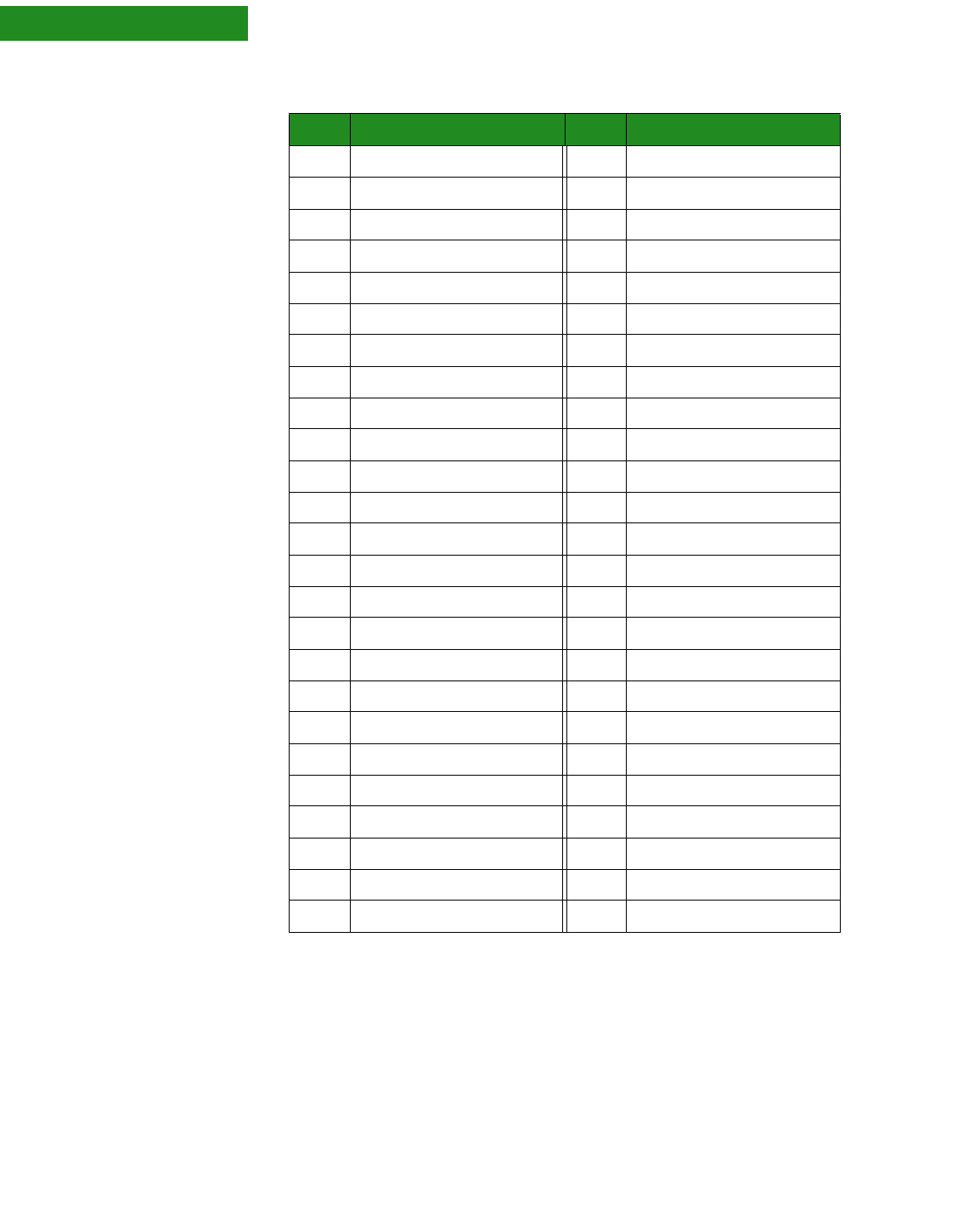
95 ConnectCore 9M 2443 & Wi-9M 2443 Hardware Reference
Chapter 2
LCD application
header, X5 Pin Signal Pin Signal
1G ND 2VD18
3 VD19 4 VD20
5 VD21 6 GND
7 VD22 8 VD23
9 VD10 10 VD11
11 GND 12 VD12
13 VD13 14 VD14
15 VD15 16 GND
17 VD21 18 VD3
19 VD4 20 VD5
21 GND 22 VD6
23 VD7 24 Reserved (LCD_D18)
25 Reserved (LCD_D19) 26 GND
27 Reserved (LCD_D20) 28 Reserved (LCD_D21)
29 I2C_SDA 30 I2C-SCL
31 GND 32 VCLK
33 VM 34 VLINE
35 VFRAME 36 EINT13
37 LCD_PWREN# 38 +3.3V
39 TSXP 40 TSYP
41 TSXM 42 TSYM
43 +3.3V 44 +3.3V
45 NC 46 NC
47 NC 48 +3.3V
49 +3.3V 50 GND
. . . . .
www.ConnectCore 9M 2443 & Wi-9M 2443 Hardware Reference.com 96
Peripheral
application
header, X3
3
Pin Signal Pin Signal
1G ND 2D0
3D1 4D2
5 D3 6 GND
7D4 8D5
9D6 10D7
11 GND 12 D8
13 D9 14 D10
15 D11 16 GND
17 D12 18 D13
19 D14 20 D15
21 GND 22 8 bit / 16 bit
+3.3V selects 8-bit data bus
23 GND 24 +3.3V
25 +3.3V 26 A0
27 A1 28 A2
29 A3 30 GND
31 A4 32 A5
33 A6 34 A7
35 GND 36 A8
37 A9 38 GND
39 CS1# 40 I2C_SDA
41 WE# 42 OE#
43 I2C_SCL 44 EINT13
45 +3.3V 46 +3.3V
47 USBPO 48 USBNO
49 No comment 50 GND
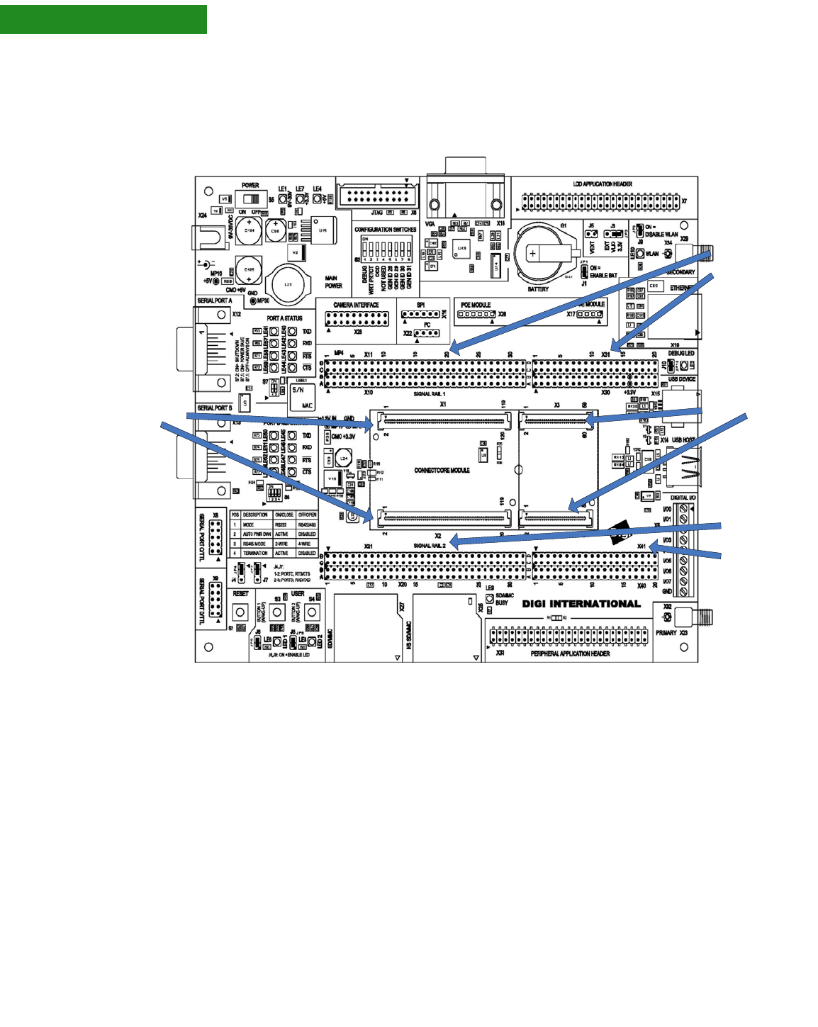
97 ConnectCore 9M 2443 & Wi-9M 2443 Hardware Reference
Chapter 2
. . . . . . . . . . . . . . . . . . . . . . . . . . . . . . . . . . . . . . . . . . . . . . . . . . . . . . . . . . . . . . . . . . . . . . . . . . . . . . . . . .
Module connectors and signal rails
Signal rails The development board provides two 4x32 pin signal rails, labeled x10/X11 and
X20/X21. These connectors are 1:1 copies of the modules pins and can be used for
measurement or development purposes.
X10 and X11 correspond to module connector X1.
X20 and X21 corresponds to module connector X2.
The development board also provides two 4x20 pin test connectors for extended
footprint modules:
X30 and X31 correspond to extended module connector X3.
X40 and X41 correspond to extended module connector X4.
Module
connectors
X1 and X2
Signal rails
X10, X11,
X30 and
X31
Signal rails
X20, X21,
X40 and
X41
Extended
module
connectors
X3 and X4

. . . . .
www.ConnectCore 9M 2443 & Wi-9M 2443 Hardware Reference.com 98
X10 pinout
Pin Signal Pin Signal
A1 G ND B1 RSTIN#
A2 TCK B2 TMS
A3 TRST# B3 DEBUGEN#
A4 CONF4/VD1 B4 CONF4/VD8
A5 CONF7/VD17 B5 TXDO
A6 CTS0# B6 NC
A7 RXD2 B7 RTS2#/TXD3
A8 CAMDATA0 B8 CAMDATA1
A9 CAMFDATA4 B9 CAMDATA5
A10 USB_PWREN# B10 VBUSDET
A11 VD3 B11 VD4
A12 VD7 B12 CF_CD#
A13 VD11 B13 VD12
A14 VD15 B14 EINT14
A15 VD19 B15 VD20
A16 VD23 B16 LCD_PWREN#
A17 VLINE B17 VCLK
A18 LCDVF1 B18 LCDVF2
A19 WLAN_DISABLE# B19 WACT_LED#
A20 SDDATA0 B20 SDDATA1
A21 SDDATA3 B21 USERKEY1/EINT0
A22 SS1# B22 SPIMISO1
A23 SD_WP# B23 SD_CD#
A24 WE# B24 WAIT#
A25 CS3# B25 CS4#
A26 NC B26 NC
A27 DQM2 B27 DQM3
A28 SPIMOS10 B28 SPICLK0
A29 USB_DT/PW B29 USBP
A30 GND B30 GND
A31 NC B31 NC
A32 +3.3V B32 +3.3V
99 ConnectCore 9M 2443 & Wi-9M 2443 Hardware Reference
Chapter 2
X11 pinout
Pin Signal Pin Signal
C1 PWRGOOD D1 RSTOUT#
C2 TDI D2 TDO
C3 NAND_FWP# D3 CONF2/VD0
C4 CONF5/VD9 D4 CONF6/VD16
C5 RXD0 D5 RTS0#
C6 NC D6 TXD2
C7 RXD2 D7 NC
C8 CTS2#/RXD3 D8 CAMDATA3
C9 CAMDATA6 D9 CAMDATA7
C10 GND D10 VD2
C11 VD5 D11 VD6
C12 EINT11 D12 VD10
C13 VD13 D13 VD14
C14 TCLK0 D14 VD18
C15 VD21 D15 VD22
C16 VM D16 VFRAME#
C17 LEND D17 LCDVF0
C18 TOUT0 D18 TOUT1
C19 SDCLK D19 SDCMD
C20 GND D20 SDDATA2
C21 X1.83 D21 DEBUG_LED
C22 USERLED1/SPIMOSI1 D22 USERLED2/SPICLK1
C23 X1.91 D23 OE#
C24 CS1# D24 CS2#
C25 PWREN D25 BATT_FLT#
C26 DQM0 D26 DQM1
C27 SS0# D27 SPIMISO0
C28 I2C_SCL D28 I2C_SDA
C29 USBN D29 VRTC
C30 VLIO D30 VLIO
C31 NC D31 NC
C32 +3.3V D32 +3.3V

. . . . .
www.ConnectCore 9M 2443 & Wi-9M 2443 Hardware Reference.com 100
X20 pinout
Pin Signal Pin Signal
A1 USBP0 B1 GND
A2 A1 B2 A2
A3 A5 B3 A6
A4 A9 B4 A10
A5 A13 B5 A14
A6 A17 B6 A18
A7 A21 B7 A22
A8 A25 B8 X2-30
A9 RXD1 B9 RTS1#
A10 XDREQ1# B10 XDACK0#
A11 AIN4 B11 AIN5
A12 AIN2 B12 AIN3
A13 AIN8/XM B13 AIN9/XP
A14 NC B14 NC
A15 XBREQ# B15 XBACK#
A16 I2SSDO/ACDO B16 I2SSDI/ACDI
A17 I2SLRCK/AC_RESET#GPEO B17 NC
A18 LEDSPD B18 NC
A19 OE_CF# B19 WE_CF#
A20 REG_CF# B20 SDDATA1
A21 D0 B21 D1
A22 D4 B22 D5
A23 D8 B23 D9
A24 D12 B24 D13
A25 SD1_DAT0 B25 SD1_DAT1
A26 SD1_DAT4 B26 SD1_DAT5
A27 SD1_CMD B27 SD1_CLK
A28 SD1_LED# B28 USERKEY2/EINT6
A29 X2.113 B29 X2.114
A30 X1.117 B30 X2.118
A31 VLIO B31 VRTC
A32 +3.3V B32 +3.3V
101 ConnectCore 9M 2443 & Wi-9M 2443 Hardware Reference
Chapter 2
X21 pinout
Pin Signal Pin Signal
C1 USBN0 D1 A0
C2 A3 D2 A4
C3 A7 D3 A8
C4 A11 D4 A12
C5 A15 D5 A16
C6 A19 D6 A20
C7 A23 D7 A24
C8 NC D8 TXD1
C9 CTS1# D9 XDREQ0#
C10 XDACK1# D10 GND
C11 AIN0 D11 AIN1
C12 AIN6YM D12 AIN7/YP
C13 AVCC D13 AGND
C14 NC D14 NC
C15 USBHOPEN D15 PME
C16 I2SCDCLK/AC_BIT_CLK D16 I2SSCLK/AC_SYNC/GPE1
C17 LEDLNK D17 NC
C18 FULLED# D18 NC
C19 IREQ_CF# D19 INPACK_CF#
C20 CF_PWEN D20 GND
C21 D2 D21 D3
C22 D6 D22 D7
C23 D10 D23 D11
C24 D14 D24 D15
C25 SDI_DAT2 D25 SD1_DAT3
C26 SD1_DAT6 D26 SD1_DAT7
C27 SD1_WP# D27 SD1_CD#
C28 EINT13 D28 X2.112
C29 X2.115 D29 CLKOUT1
C30 BCLKOUT0 D30 GND
C31 GND D31 GND
C32 +3.3V D32 +3.3V
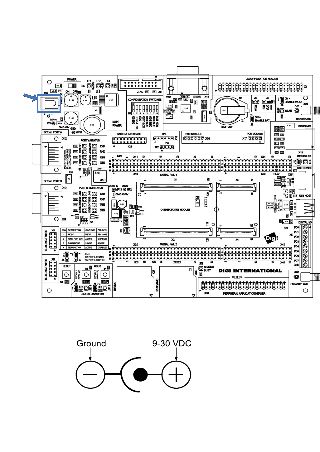
. . . . .
www.ConnectCore 9M 2443 & Wi-9M 2443 Hardware Reference.com 102
. . . . . . . . . . . . . . . . . . . . . . . . . . . . . . . . . . . . . . . . . . . . . . . . . . . . . . . . . . . . . . . . . . . . . . . . . . . . . . . . . .
Power connector
The power connector is a barrel connector with a 9-30VDC operating range. The
power jack is labeled X24 on the development board. The figure below represents
the power jack polarity.
Power
connector
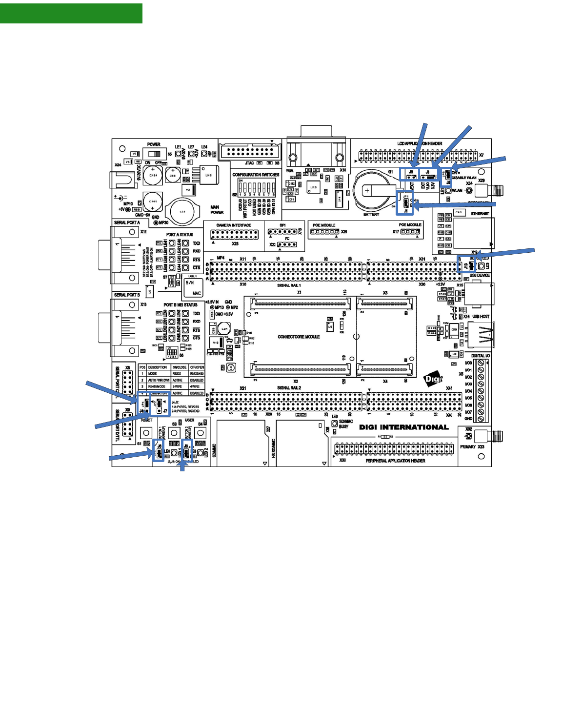
103 ConnectCore 9M 2443 & Wi-9M 2443 Hardware Reference
Chapter 2
. . . . . . . . . . . . . . . . . . . . . . . . . . . . . . . . . . . . . . . . . . . . . . . . . . . . . . . . . . . . . . . . . . . . . . . . . . . . . . . . . .
Jumpers
External VLIO
supply J5
WLAN
disable J9
VLIO power
source J3
Battery
Jumper
J1
Debug LED
Jumper J10
Port C
select J4
Port D
select
J7
User LED1
Jumper J6
User LED2 Jumper J8
. . . . .
www.ConnectCore 9M 2443 & Wi-9M 2443 Hardware Reference.com 104
Jumpers
Jumpe
rName Description Settings
J1 Battery Enable Supplies the real time clock with 3V
backup power from the battery
(lithium coin cell battery, G1) if the
board is switched off.
Closed =
Backup battery enabled
Open = Backup battery disabled
J3 VLIO select Select VLIO power source (+3.3V or
VEXT JT)
Pin2-3 closed VLIO = on board 3.3V
Pin1-2 closed VLIO = power
connected to J10
J4 Port C/D select
RTS2/TXD3
Select RTS2 PortC or TXD3 PortD Pin1-2 closed= RTS2
Pin2-3 closed =TXD3
J5 VEXT External power Connector for external accumulator.
Pin1 = GND Pin2 = VLIO
J6 User LED1 User LED1 enable / disable Closed = User LED1 enabled
J7 Port C/D select
CTS2/RXD3
Select CTS2 PortC or RXD3 Port D Pin1-2 closed = CTS2
Pin2-3 closed = RXD3
J8 User LED2 User LED2 enable / disable Closed = UserLED2 enabled
J9 WLAN_DISABLE# Disables the WLAN interface on the
module (if present)
Closed = WLAN disabled
Open = WLAN enabled
J13 Debug LED Debug LED enable / disable Closed = Debug LED enabled
Open = Debug LED disabled
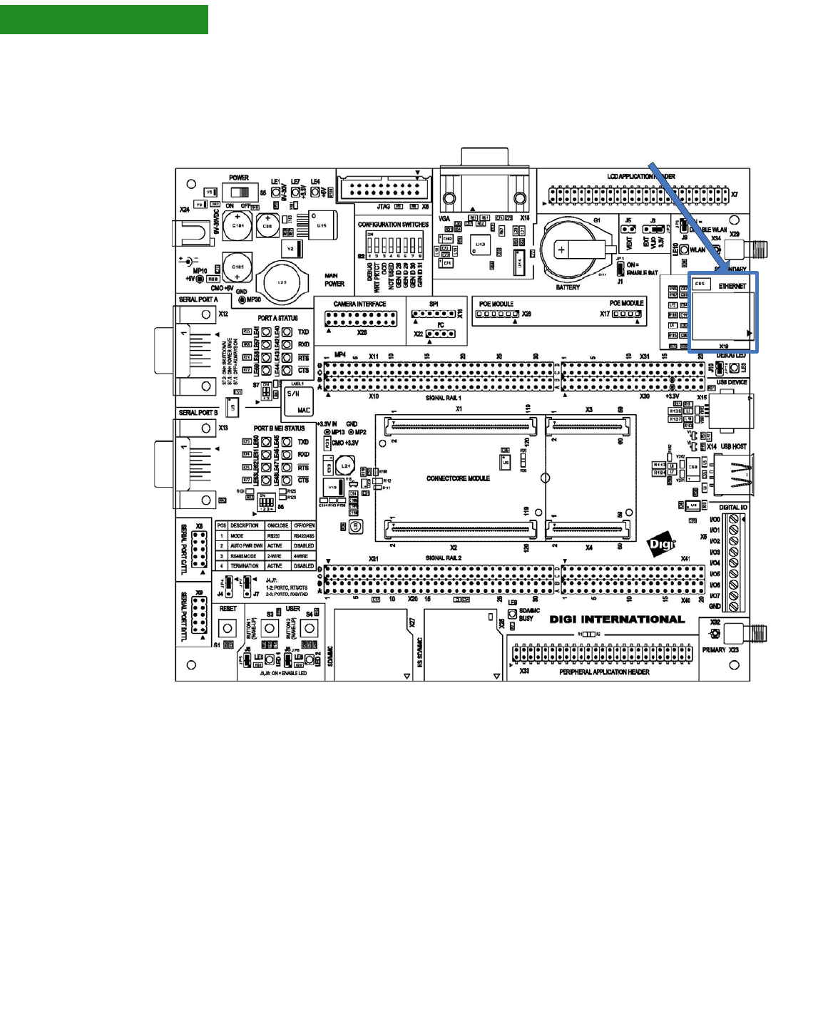
105 ConnectCore 9M 2443 & Wi-9M 2443 Hardware Reference
Chapter 2
. . . . . . . . . . . . . . . . . . . . . . . . . . . . . . . . . . . . . . . . . . . . . . . . . . . . . . . . . . . . . . . . . . . . . . . . . . . . . . . . . .
Ethernet interface
The module provides the 10/100 Ethernet MAC and PHY chip. The development
board provides the 1:1 transformer and Ethernet connector.
The Ethernet connector is an 8-wire RJ-45 jack, labeled X19, on the development
board. The connector has eight interface pins, as well as two integrated LEDs that
provide link status and network activity information.
.
Ethernet RJ-45, X19
. . . . .
www.ConnectCore 9M 2443 & Wi-9M 2443 Hardware Reference.com 106
RJ-45 pin
allocation, X7 RJ-45 connector pins are configured as shown:
Pin Signal 802.3af End-Span
(mode A) 802.3af Mid-Span
(Mode B) Description
1 TXD+ Negative VPort Transmit data +
2 TXD- Negative VPort Transmit data -
3 RXD+ Positive VPort Receive data +
4 EPWR+ Positive VPort Power from switch
5 EPWR+ Positive VPort Power from switch +
6 RXD- Positive VPort Receive data -
7 EPWR NegativeVPort Power from switch -
8 EPWR NegativeVPort Power from switch -
LED Description
Yellow Network activity (speed):
-Flash indicates network traffic detected
-Off indicates no network traffic detected
Green Network link:
-On indicates an active network link
-Off indicates no network link is present
107 ConnectCore 9M 2443 & Wi-9M 2443 Hardware Reference
Chapter 2
Pin Name DeComment
1+3.3VPower
2GND
3 CMDATA0 camera data
4 CMDATA1 camera data
5 CMDATA2 camera data
6 CMDATA3 camera data
7 CMDATA4 camera data
8 CMDATA5 camera data
9 CMDATA6 camera data
10 CMDATA7 camera data
11 CAMCLKOUT Master clock to the camera processor
12 CAMPCLK Pixel clock driven by the camera processor
13 CAM_HREF Horizontal sync driven by camera procesor
14 CAMVSUNC Frame sync driven by camera processor
15 I2C_SCL I2C bus for initialization
16 I2C_SDA I2C bus for initialization
17 XDACK0# GPIO (not used)
18 CAMRESET Reset to the camera processor
19 GND
20 +5V Power (not used)
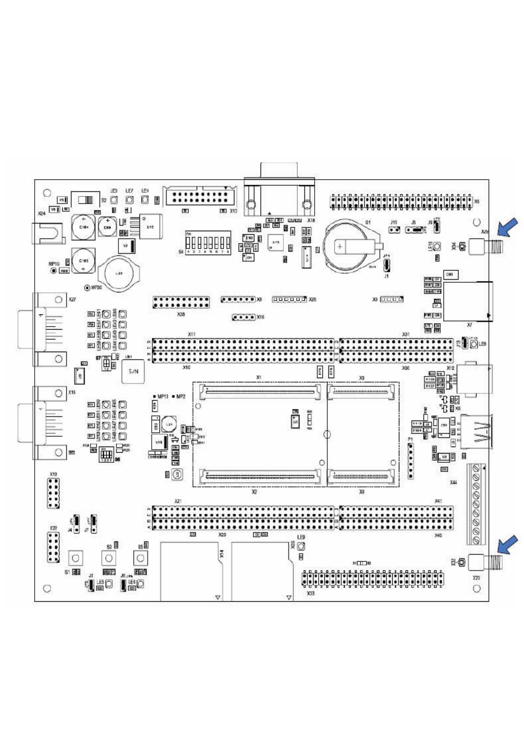
. . . . .
www.ConnectCore 9M 2443 & Wi-9M 2443 Hardware Reference.com 108
. . . . . . . . . . . . . . . . . . . . . . . . . . . . . . . . . . . . . . . . . . . . . . . . . . . . . . . . . . . . . . . . . . . . . . . . . . . . . . . . . .
WLAN Interface
For the ConnectCore Wi-9M 2443, attach the antenna to the primary connector
[X23] and the secondary connector [X34] on the development board. See figure
below.
109 ConnectCore 9M 2443 & Wi-9M 2443 Hardware Reference
Chapter 2
. . . . . . . . . . . . . . . . . . . . . . . . . . . . . . . . . . . . . . . . . . . . . . . . . . . . . . . . . . . . . . . . . . . . . . . . . . . . . . . . . .
Interfaces without special connectors
ADC signals
CF signals
ADC Signals ADC signals are accessible on the signal rails (no dedicated connector).
CF Signals Compact Flash signals are accessible on the signal rails (no dedicated
connector).
I2S/AC97 Signals Audio I2S/AC97 signals are accessible on the signal rails (no dedicated
connector).
SPI1 Signals The standard speed SPI1 signals are accessible on the signal rails (no
dedicated connector).
Signal name Signal rail
AIN0 X21 C11
AIN1 X21 D11
AIN2 X20 A12
AIN3 X20 B12
AIN4 X20 A11
AIN5 X20 B11
AIN6/YM X21 C12
AIN7/YP X21 D12
AIN8/XM X20 A13
AIN9/XP X210 B13
Signal name Signal rail
CF_OE# X20 A19
CF_WE# X20 B19
CF_IREQ# X21 C19
CF_INPACK# X21 D19
CF_PWEN# X21 C20
CF_REG# X20 A20
CF_RESET# X20 B20
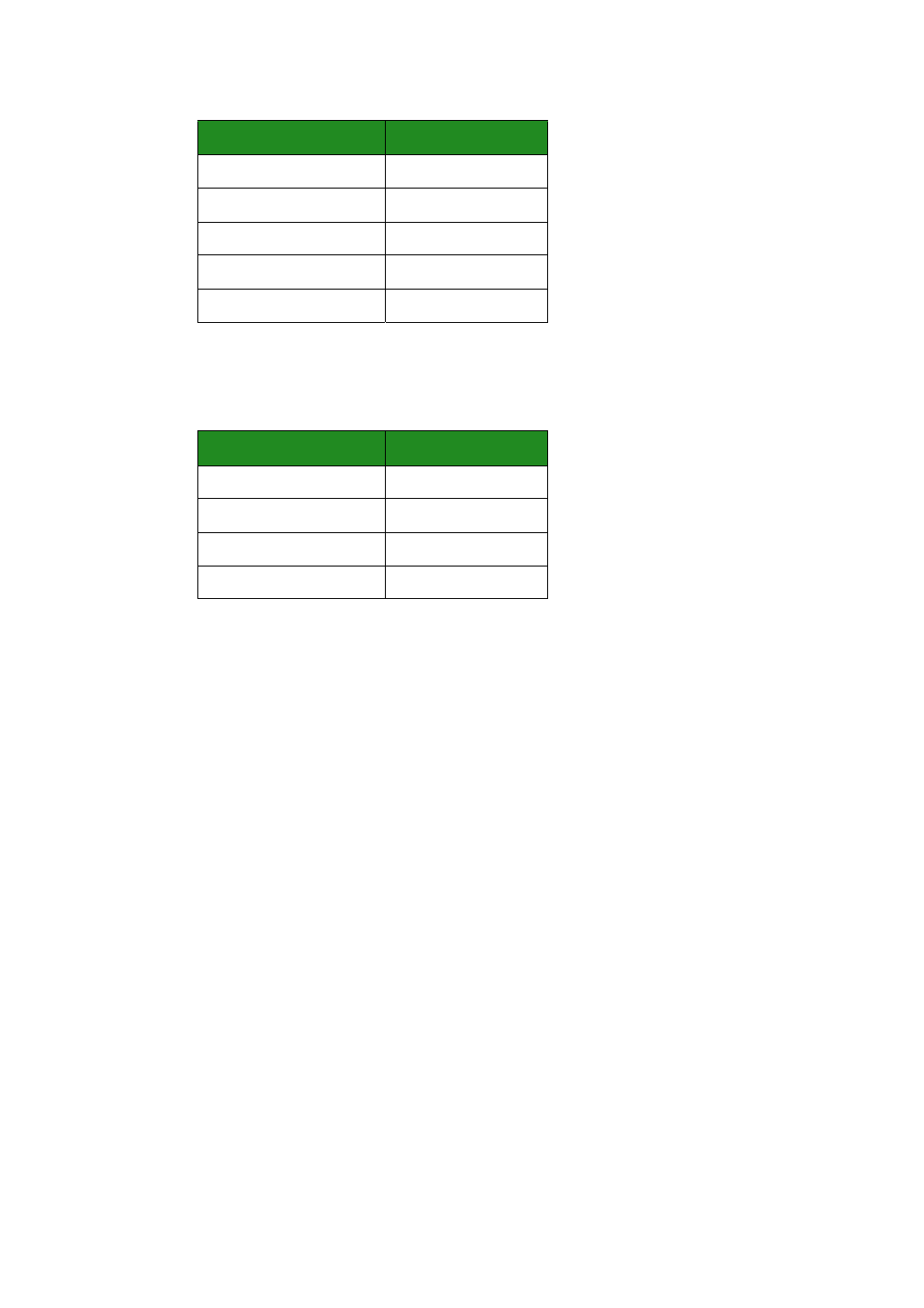
. . . . .
www.ConnectCore 9M 2443 & Wi-9M 2443 Hardware Reference.com 110
I2S/AC97 signals
SPI1 signal
An expansion board is available for the ADC, CF, I2S/AC97, and SPI1 signals above.
Signal name Signal rail
I2SLRCK/AC_RESET# X20 A17
I2SSCLK/AC_SYNC X21 D16
I2SCDCLK/AC_BIT_CLK X21 C16
I2SSDI/ACDI X20 B16
I2SSDO/ACDO X20 A16
Signal name Signal rail
SPIMOSI1 X21 D28
SPIMISO1 X20 B28
SPICLK1 X21 C28
SS1# X21 C29

111 ConnectCore 9M 2443 & Wi-9M 2443 Hardware Reference
Chapter 2
. . . . . . . . . . . . . . . . . . . . . . . . . . . . . . . . . . . . . . . . . . . . . . . . . . . . . . . . . . . . . . . . . . . . . . . . . . . . . . . . . .
Module and test connectors
X1 pinout The ConnectCore 9M 2443 module plugs into the module connectors X1 and X2 on
the development board.AI = Analog Input
I = Input
O = Output
I/O = Input or Output
P = Power
REF = Analog Reference Voltage
X1 Type U-Boot Module
Functionality Comments Usage on
development board
1 P - GND GND
2 I - RSTIN# Reset input, i.e
Push Button on the
module this signal
is the input to a
reset controller.
Pull-up 10k to
+3.3V already on
module.
Push button with 10k pull-up
3 I/O - PWRGOOD Output of the reset
controller push
pull with 470R
current limiting
resistor
4 O - RSTOUT# Output of CPU.
Softw + WDt +
rstin#
5 I - TCK JTAG, Pull-up
10k to +3.3V on
module
"JTAG connector X13
6 I - TMS JTAG, Pull-up
10k to +3.3V on
module
"JTAG connector X13
7 I - TDI JTAG, Pull-up
10k to +3.3V on
module
"JTAG connector X13
8 O - TDO JTAG, Pull-up
10k to +3.3V on
module
"JTAG connector X13

. . . . .
www.ConnectCore 9M 2443 & Wi-9M 2443 Hardware Reference.com 112
9 I - TRST# JTAG, Pull-up
10k to +3.3V on
module
"JTAG connector X13
10 I - CONF0#
DEBUGEN#
Debug enable,
Pull-up 10k to
+3.3V on module
0 = Debug
enabled, TRST#
isolated from
PWRGOOD
Conneected to DIP-switch
S2.1
ON: connected to GND
11 I - CONF1
NAND_FWP#
NAND Flash
Write Protect,
Pull-up 10k to
+3.3V on module
0 = NAND Flash
write protected
Connected to DIP-switch S4.2
ON: connected to GND
12 I I- CONF2
VD0
GPC8
Pull-up 10k to
+3.3V on module Connected to DIP-switch S4.3
ON: connected to GND
13 I I CONF3
VD1
GPC9
Reserved, do not
connect, Pull-up
10k to +3.3V on
module
Connected to DIP-switch S4.4
ON: connected to GND
14 I/O I CONF4
VD8
GPD0
Pull-up 10k to
+3.3V on module Connected to DIP-switch S4.5
ON: connected to GND
15 I/O I CONF5
VD9
GPD1
Pull-up 10k to
+3.3V on module Connected to DIP-switch S4.6
ON: connected to GND
16 I/O I CONF6
VD16
GPD8
Pull-up 10k to
+3.3V on module Connected to DIP-switch S4.7
ON: connected to GND
17 I/O I CONF7
VD17
GPD9
Pull-up 10k to
+3.3V on module Connected to DIP-switch S4.8
ON: connected to GND
18 I/O TxD0 TxD0
GPH0
Configured to
TxD0 Connected via RS232 driver to
COMA, X27
19 I/O RxD0 RxD0
GPH1
Configured to
RxD0 Connected via RS232 driver to
COMA, X27
20 I/O RTS0# RTS0#
GPH9
Configured to
RTS0# Connected via RS232 driver to
COMA, X27
21 I/O CTS0# CTS0#
GPH8
Configured to
CTS0# Connected via RS232 driver to
COMA, X27
X1 Type U-Boot Module
Functionality Comments Usage on
development board
113 ConnectCore 9M 2443 & Wi-9M 2443 Hardware Reference
Chapter 2
22 I/O CAMPCLK CAMPCLK
GPJ8
Pixel clock, driven
by the camera
processor, input
with pull-up
enabled
Connected to X28
23 I/O CAM_HREF CAM_HREF
GPJ10
Horizontal Sync,
driven by the
camera processor,
input with pull-up
enabled
Connected to X28
24 I/O TxD2 TxD2
GPH4
Configured to
TxD2 TxD2 connected to COMC,
X19
25 I/O RxD2 RxD2
GPH5
Configured to
RxD2 TxD2 connected to COMC,
X19
26 I/O RTS2# RTS2#
GPH6
TxD3
Configured to
RTS2#, could also
be used as TxD3
Connected to J4
27 I/O CTS2# CTS2#
GPH7
RxD3
Configured to
CTS2#, could also
be used as RxD3
Connected to J7
28 I/O CAMVSYNC CAMVSYNC
GPJ9
Frame Sync,
driven by the
camera processor,
input with pull-up
enabled
Connected to X28
29 I/O CAMDATA0 CAMDATA0
GPJ0
Pixel Data driven
by camera
processor, input
with pull-up
enabled
Connected to X28
30 I/O CAMDATA1 CAMDATA1
GPJ1
Pixel data driven
by the camera
processor, input
with pull-up
enabled
Connected to X28
31 I/O CAMDATA2 CAMDATA2
GPJ2
Pixel data driven
by the camera
processor, input
with pull-up
enabled
Connected to X28
32 I/O CAMDATA3 CAMDATA3
GPJ3
Pixel data driven
by the camera
processor, input
with pull-up
enabled
Connected to X28
X1 Type U-Boot Module
Functionality Comments Usage on
development board

. . . . .
www.ConnectCore 9M 2443 & Wi-9M 2443 Hardware Reference.com 114
33 I/O CAMDATA4 CAMDATA4
GPJ4
Pixel data driven
by the camera
processor, input
with pull-up
enabled
Connected to X28
34 I/O CAMDATA5 CAMDATA5
GPJ5
Pixel data driven
by the camera
processor, input
with pull-up
enabled
Connected to X28
35 I/O CAMDATA6 CAMDATA6
GPJ6
Pixel data driven
by the camera
processor, input
with pull-up
enabled
Connected to X28
36 I/O CAMDATA7 CAMDATA7
GPJ7
Pixel data driven
by the camera
processor, input
with pull-up
enabled
Connected to X28
37 O USB_PWREN# USB_PWREN#
GPA14
Configured as
output, pull-up
enabled
Switch the 5V of the USB host
connector X6
38 I VBUSDET VBUSDET
GPF5
EINT5
Configured as
input, pull-
up/interrupt
enabled
Monitors the connection of a
USB host (5V applied) at X12
39 P P GND GND
40 I/O VD2 VD2
GPC10
Configured as
output, pull-up
enabled
Connected to LCD
Application Header X5
41 I/O VD3 VD3
GPC11
Configured as
output, pull-up
enabled
Connected to LCD
Application Header X5
42 I/O VD4 VD4
GPC12
Configured as
output, pull-up
enabled
Connected to LCD
Application Header X5
43 I/O VD5 VD5
GPC13
Configured as
output, pull-up
enabled
Connected to LCD
Application Header X5
44 I/O VD6 VD6
GPC14
Configured as
output, pull-up
enabled
Connected to LCD
Application Header X5
45 I/O VD7 VD7
GPC15
Configured as
output, pull-up
enabled
Connected to LCD
Application Header X5
X1 Type U-Boot Module
Functionality Comments Usage on
development board
115 ConnectCore 9M 2443 & Wi-9M 2443 Hardware Reference
Chapter 2
46 I CF_CD# CF_CD#
GPG10
EINT18
Configured as
input, pull-
up/interrupt
disabled
Card detect CF_CD when Add
on Board is applied
47 - I GPG3
EINT11
Configured as
input, pull-
up/interrupt
disabled
Not used, connected to
X11;C12
48 I/O VD10 VD10
GPD2
Configured as
output, pull-up
enabled
Connected to LCD
Application Header X5
49 I/O VD11 VD11
GPD3
Configured as
output, pull-up
enabled
Connected to LCD
Application Header X5
50 I/O VD12 VD12
GPD4
Configured as
output, pull-up
enabled
Connected to LCD
Application Header X5
51 I/O VD13 VD13
GPD5
Configured as
output, pull-up
enabled
Connected to LCD
Application Header X5
52 I/O VD14 VD14
GPD6
Configured as
output, pull-up
enabled
Connected to LCD
Application Header X5
53 I/O VD15 VD15
GPD7
Configured as
output, pull-up
enabled
Connected to LCD
Application Header X5
54 I - GPG6
EINT14
Configured as
input, pull-up
enabled
Not used, connected to
X10;B14
55 I - GPB4
TCLK0
Configured as
input Not used, connected to
X11;C14
56 I/O VD18 GPB4
TCLK0
Configured as
output, pull-up
enabled
Connected to LCD
Application Header X5
57 I/O VD19 VD19
GPD11
Configured as
output, pull-up
enabled
Connected to LCD
Application Header X5
58 I/O VD20 VD20
GPD12
Configured as
output, pull-up
enabled
Connected to LCD
Application Header X5
59 I/O VD21 VD21
GPD13
Configured as
output, pull-up
enabled
Connected to LCD
Application Header X5
X1 Type U-Boot Module
Functionality Comments Usage on
development board

. . . . .
www.ConnectCore 9M 2443 & Wi-9M 2443 Hardware Reference.com 116
60 I/O VD22 VD22
GPD14
Configured as
output, pull-up
enabled
Connected to LCD
Application Header X5
61 I/O VD23 VD23
GPD15
Configured as
output, pull-up
enabled
Connected to LCD
Application Header X5
62 I/O LCD_PWRE N LCD_PWREN
GPG4
EINT12
Configured as
output, pull-up
disabled
Connected to LCD
Application Header X5
63 I/O VM VM
GPC4
Configured as
output, pull-up
disabled
Connected to LCD
Application Header X5
64 I/O VFRAME VFRAME
GPC3
Configured as
output, pull-up
disabled
Connected to LCD
Application Header X5
65 I/O VLINE VLINE
GPC2
Configured as
output, pull-up
disabled
Connected to LCD
Application Header X5
66 I/O VCLK VCLK Configured as
output, pull-up
disabled
Connected to LCD
Application Header X5
67 I/O LEND LEND
GPC0
Configured as
input, pull-up
enabled
Not used
68 I/O LCD_LPCOE LCD-VFO
GPC5
Configured as
output, pull-up
disabled
Connected to LCD
Application Header X5
69 I/O LCD_LPCREV LCD_VF1
GPC6
Configured as
output, pull-up
disabled
Connected to LCD
Application Header X5
70 I/O LCD_LPCREVB LCD_VF2
GPC7
Configured as
output, pull-up
disabled
Connected to LCD
Application Header X5
71 I/O TOUT0 TOUT0
GPB0
Configured as
output, pull-up
disabled
Not used, connected to
X11;C18
72 I/O TOUT1 TOUT1
GPB1
Configured as
output, pull-up
disabled
Not used, connected to
X11;D18
73 - - WLAN_DISABL
E# Reserved for
CCW9M2443 Connected to Jumper J9
(set=disabled)
74 - - WACT_LED# Reserved for
CCW9M2443 Connected to LE10(low=on)
X1 Type U-Boot Module
Functionality Comments Usage on
development board

117 ConnectCore 9M 2443 & Wi-9M 2443 Hardware Reference
Chapter 2
75 I/O SDCLK SD0CLK
GPE5
SD0 card detect Connected to SD connector
X14
76 I/O SD0CMD/GPE6 SDCMD/GPE6 10k pull-up on
base board Connected to SD connector
X14
77 I/O SDDATA0 SD0DATA0
GPE7
10k pull-up on
base board Connected to SD connector
X14
78 I/O SDDATA1 SD0DATA1
GPE8
10k pull-up on
base board Connected to SD connector
X14
79 P - GND GND
80 I/O SDDATA2 SD0DATA2
GPE9
10k pull-up on
base board Connected to SD connector
X14
81 I/O SDDATA3 SD0DATA3
GPE10
10k pull-up on
base board Connected to SD connector
X14
82 I/O EINT0
GPF0
EINT0/GPF0 Configured as
input, pull-up
disabled
Connected to User Key 1
83 - - NC Connected to X11;C21
84 I/O TOUT2 TOUT2
GPB2
DEBUG LED Connected to JP13 (open=NC)
85 I/O SS1# GPL14
SS1#
Configured as
input, pull-up
enabled
Connected to X10;A22
86 I/O SPIMISO1 GPL12
SPIMISO1
Configured as
input, pull-up
enabled
Connected to X10;B22
87 I/O SPIMOSI1 USERLED1
SPIMOSI1
GPL11
Configured as
output, pull-up
enabled
Connected toUSERLED1
88 I/O O USERLED2
SPICLK1
GPL10
Configured as
output, pull-up
enabled
Connected to USERLED2
89 I/O SD_WP# EINT17
GPG9
Configured as
input, pull-up
disabled
Write protect
Connected to SD connector
X14
X1 Type U-Boot Module
Functionality Comments Usage on
development board

. . . . .
www.ConnectCore 9M 2443 & Wi-9M 2443 Hardware Reference.com 118
90 I/O SD_CD# EINT1/GPF1 Configured as
input, pull-up
disabled
Card detect
Connected to X14
91 - - NC Connected to X11;C23
92 O ROE# OE# 22R series resistor
on module Connected to X33 Peripheral
Application Header
93 O RWE# WE# 22R series resistor
on module Connected to X33 Peripheral
Application Header
94 I WAIT# WAIT# Pullup 5k to
+3.3V on module Not used
95 I/O RCS1# RCS1# Chip select, not
used on module,
22R series resistor
on module.
Defaults to
Output/High at
reset
Connected to X33 Peripheral
Application Header
96 I/O RCS2# RCS2# Chip select, not
used on module,
22R series resistor
on module.
Defaults to
Output/High at
reset
Not used
97 I/O RCS3# RCS3# Chip select, not
used on module,
22R series resistor
on module,
defaults to
Output/High at
reset
Not used
98 I/O RCS4# RCS4# Chip select, used
on CCW9M2443
module for
wireless LAN.
Not used
99 O - PWREN 1.3V power
control signal
0 = Power for
unneeded parts is
switched off
Must be left
unconnected if not
used
Connected to CPLD
X1 Type U-Boot Module
Functionality Comments Usage on
development board

119 ConnectCore 9M 2443 & Wi-9M 2443 Hardware Reference
Chapter 2
100 I - BATT_FLT# Battery fault
Pull-up 10k to
+3.3V on module,
can be left
unconnected.
Not used
101 I/O CAMCLKOUT CAMPCLKOUT
GPJ11
Master clock to
the camera
processor output
with pull-up
enabled
Connected to X28
102 I/O CAMRESET CAMRESET
GPJ12
Software reset or
power down to the
camera processor
output with pull-
up enabled
Connected to X28
103 O - RBEO# Upper
Byte/Lower Byte
Enable
Not used
104 O - RBE1# Not used
105 O - Not used
106 O - Not used
107 I/O SS0# SS0#GPL13 SPI0, pull-up
enabled Connected to X8 SPI
connector
108 I/O SPIMISO0 SPIMISO0
GPE11
Pull-up enabled Connected to X8 SPI
connector
109 I/O SPIMOS10 SPIMOSI0
GPE12
Pull-up enabled Connected to X8 SPI
connector
110 I/O SPICLK0 SPICLK0
GPE13
Pull-up disabled Connected to X8 SPI
connector
111 I/O IICSCL IICSCL
GPE14
I2C clock, pullup
4k7 to 3.3V on
module
Connected to X33, X28, X15,
U5, U7
112 I/O IICSDA IICSDA
GPE15
I2C clock, pullup
4k7 to 3.3V on
module
Connected to X33, X28, X15,
U5, U7
113 I/O O USB_DT/PW
GPG0
EINT8
Default GPG0
input. Optional output to switch on
1k5 pull-up resistor for USB
device (CC9M2440
compatibility)
114 I/O USBP DP_UDEV USB device USB device data line +
connected to X12
X1 Type U-Boot Module
Functionality Comments Usage on
development board

. . . . .
www.ConnectCore 9M 2443 & Wi-9M 2443 Hardware Reference.com 120
115 I/O USBN DN_UDEV USB device USB device data line -
connected to X12
116 P - VRTC Backup battery for
RTC, for 3V cell,
power-switch-
over is on the
module. Can be
left floating, if
RTC backup is not
needed.
3V battery connected
117 P - GND GND
118 P - +3.3V +3.3V
119 P - VLIO Mobile: Power
from Li-Ion
Battery
Non-Mobile:
connected to 3.3V
Delivers either power from Li-
Ion battery or 3.3V
120 P - +3.3V +3.3V
X1 Type U-Boot Module
Functionality Comments Usage on
development board
121 ConnectCore 9M 2443 & Wi-9M 2443 Hardware Reference
Chapter 2
X2 pinout AI = Analog Input
I = Input
O = Output
I/O = Input or Output
P = Power
REF = Analog Reference Voltage
X2 Typ
eU-
Boot Module
Functionality Comments Usage on
development board
1 I/O USBP0 USBP0 USB host0, 22R series resistor
has to be mounted on base
board.
USB host data line +,
connected to X6
2 P - GND GND
3I/OUSBN
0USBN0 USB host0, 22R series resistor
has to be mounted on base
board.
USB host data line -,
connected to X6
4 O A0 RADDR0
GPA0
Used as address of ETH-Contr.
on module. Should not be used
as I/O pin for compatibility.
Connected to X33 Peripheral
Application header
5 O A1 RADDR1 Used as address of ETH-Contr.
on module. Connected to X33 Peripheral
Application header
6 O A2 RADDR2 Used as address of ETH-Contr.
on module and WM500ABG. Connected to X33 Peripheral
Application header
7 O A3 RADDR3 Used as address of ETH-Contr.
on module and WM500ABG. Connected to X33 Peripheral
Application header
8 O A4 RADDR4 Used as address of ETH-Contr.
on module and WM500ABG. Connected to X33 Peripheral
Application header
9 O A5 RADDR5 Used as address of ETH-Contr.
on module and WM500ABG. Connected to X33 Peripheral
Application header
10 O A6 RADDR6 Used as address of ETH-Contr.
on module and WM500ABG. Connected to X33 Peripheral
Application header
11 O A7 RADDR7 Used as address of
WM500ABG. Connected to X33 Peripheral
Application header
12 O A8 RADDR8 Connected to X33 Peripheral
Application header
13 O A9 RADDR9 Connected to X33 Peripheral
Application header
14 O A10 RADDR10 Not used
15 O A11 RADDR11 Not used
16 O A12 RADDR12 Not used

. . . . .
www.ConnectCore 9M 2443 & Wi-9M 2443 Hardware Reference.com 122
17 O A13 RADDR13 Not used
18 O A14 RADDR14 Used as address of ETH-Contr.
on module Not used
19 O A15 RADDR15 Not used Not used
20 O A16 RADDR16
GPA1
should not be used as I/O pin
for compatibility Not used
21 O A17 RADDR17
GPA2
should not be used as I/O pin
for compatibility Not used
22 O A18 RADDR18
GPA3
should not be used as I/O pin
for compatibility Not used
23 O A19 RADDR19
GPA4
should not be used as I/O pin
for compatibility Not used
24 O A20 RADDR20
GPA5
should not be used as I/O pin
for compatibility Not used
25 O A21 RADDR21
GPA6
should not be used as I/O pin
for compatibility Not used
26 O A22 RADDR22
GPA7
should not be used as I/O pin
for compatibility Not used
27 O A23 RADDR23
GPA8
should not be used as I/O pin
for compatibility Not used
28 O A24 RADDR24
GPA9
should not be used as I/O pin
for compatibility Not used
29 O A25 RADDR25
GPA10
should not be used as I/O pin
for compatibility Not used
30 O - Pull down Not used
31 - RXD1 RXD1
GPH3
PortB RxD Connected to PortB MEI
32 - TXD1 TXD1
GPH2
PortB TxD Connected to PortB MEI
33 - CTS1# CTS1#
GPH10
Port CTS Connected to PortB MEI
34 - RTS1# RTS1#
GPH11
Port RTS Connected to PortB MEI
35 - - Not connected
36 I/O I XDREQ0#
GPB10
Configured as input, pull-up
enabled Not used
37 I/O I XDREQ1#
GPB8
Configured as input, pull-up
enabled Not used
X2 Typ
eU-
Boot Module
Functionality Comments Usage on
development board

123 ConnectCore 9M 2443 & Wi-9M 2443 Hardware Reference
Chapter 2
38 I/O I XDACK0#
GPB9
Configured as input, pull-up
enabled Not used
39 I/O I XDACK1#
GPB7
Configured as input, pull-up
enabled Not used
40 P - GND GND
41 AI - AIN4 Analog in. Unused analog
inputs should be
connected to AGND over a
10k series resistor
to avoid cross over.
Not used
42 AI -
-
AIN5 Analog in. Unused analog
inputs should be
connected to AGND over a
10k series resistor
to avoid cross over.
Not used
43 AI - AIN0 Analog in. Unused analog
inputs should be connected to
AGND over a 10k series
resistor to avoid cross over.
Not used
44 AI - AIN1 Analog in. Unused analog
inputs should be
connected to AGND over a
10k series resistor
to avoid cross over.
Not used
45 AI - AIN2 Analog in. Unused analog
inputs should be
connected to AGND over a
10k series resistor
to avoid cross over.
Not used
46 AI - AIN3 Analog in, unused analog
inputs should be connected to
AGND over a 10k series
resistor to avoid cross over.
Not used
47 AI - AIN6/YM Used for touch screen
TSYM/JSCC9M2443 Connected to LCD.
Application connector X5.
48 AI - AIN7/YP Used for touch screen
TSYP/JSCC9M2443 Connected to LCD.
Application connector X5.
49 AI - AIN8/XM Used for touch screen
TSXM/JSCC9M2443 Connected to LCD.
Application connector X5.
50 AI - AIN9/XP Used for touch screen
TSXP/JSCC9M2443 Connected to LCD.
Application connector X5.
X2 Typ
eU-
Boot Module
Functionality Comments Usage on
development board

. . . . .
www.ConnectCore 9M 2443 & Wi-9M 2443 Hardware Reference.com 124
51 REF - AVCC Analog VCC. Is the extra
filtered +3.3V
connected with the AVCC ball
of the CPU.
Can be used as an analog
reference;
do not connect to any other
power source.
Used for AIN0-9
52 REF - AGND Analog GND Used for AIN0-9
53 - - NC - Reserved for CCW9M2443
54 - - NC - Reserved for CCW9M2443
55 - - NC - Reserved for CCW9M2443
56 - - NC - Reserved for CCW9M2443
57 I/O I XBREQ#1
GPB6
Configured as input, pull-up
enabled Not used
58 I/O I XBACK#
GPB5
Configured as input, pull-up
enabled Not used
59 I/O I USBH0PEN
GPG8
EINT16
USB host0 Power Enable USB host: input to recognize
current limit from connected
device 0=fail
60 O - PME LAN9215 PME pin 70 Ethernet controller power
management event
61 I/O I2SSD
OI2SSDO
GPE4
AC_SDO
I2S-interface, pull-up disabled Not used
62 I/O I2SSDI I2SSDIO
GPE3
AC_SDI
I2S-interface, pull-up disabled Not used
63 I/O I2SCD
CLK I2SCDCLK
GPE2
AC_BIT_CLK
I2S-interface, pull-up disabled Not used
64 I/O I2SSC
LK I2SSCLK
GPE1
AC_SYNC
I2S-interface, pull-up disabled Not used
65 I/O I2SLR
CK GPE0
AC_RESET#
I2S-interface, pull-up disabled Not used
66 I - TPIN Ethernet 0 output-
100R differential termination
on module
Connected to RJ45 with
integrated magnetics
X2 Typ
eU-
Boot Module
Functionality Comments Usage on
development board

125 ConnectCore 9M 2443 & Wi-9M 2443 Hardware Reference
Chapter 2
67 O - LEDLNK Ethernet 0 Line/Activity LED
High, when link ok Low, while
active
Connected to Link/Activity
LED
68 I - TPIP Ethernet 0 Input+
100R differential termination
on module
Connected to X7 RJ45 with
integrated magnetics
69 O - LEDH0 speed LED Connected to X7 RJ45 LED
70 O - TPON Ethernet 0 output- 100R
differential termination on
module
Connected to X7 RJ45 with
integrated magnetics
71 I/O - ETHGPIO2/LED
3Full duplex LED/IO Not connected
72 O - TPOP Ethernet 0 Output+ 100R
differential termination on
module
Connected to X7 RJ45 with
integrated magnetics
73 O GPA11 OE_CF#
GPA11
Compact FLASH signal Not used.
74 O GPA15 WE_CF#
GPA15
Compact FLASH signal Not used.
75 I GPG11 EINT19
IREQ_CF#
GPG11
Compact FLASH signal Not used.
76 I GPG12 EINT20
INPACK#
GPG12
Compact FLASH signal Not used.
77 O GPG13 EINT21
REG_CF#
GPG13
Compact FLASH signal Not used.
78 O GPG14 EINT22
RESET_CF
GPG14
Compact FLASH signal Not used.
79 O GPG15 EINT23
CF_PWREN
GPG15
Compact FLASH signal Not used.
80 P - GND GND
81 I/O D0 RDATA0 Data Bus Connected to X33 Peripheral
Application Header
82 I/O D1 RDATA1 Connected to X33 Peripheral
Application Header
83 I/O D2 RDATA2 Connected to X33 Peripheral
Application Header
X2 Typ
eU-
Boot Module
Functionality Comments Usage on
development board

. . . . .
www.ConnectCore 9M 2443 & Wi-9M 2443 Hardware Reference.com 126
84 I/O D3 RDATA3 Connected to X33 Peripheral
Application Header
85 I/O D4 RDATA4 Connected to X33 Peripheral
Application Header
86 I/O D5 RDATA5 Connected to X33 Peripheral
Application Header
87 I/O D6 RDATA6 Connected to X33 Peripheral
Application Header
88 I/O D7 RDATA7 Connected to X33 Peripheral
Application Header
89 I/O D8 RDATA8 Connected to X33 Peripheral
Application Header
90 I/O D7 RDATA9 Connected to X33 Peripheral
Application Header
91 I/O D10 RDATA10 Connected to X33 Peripheral
Application Header
92 I/O D11 RDATA11 Connected to X33 Peripheral
Application Header
93 I/O D12 RDATA12 Connected to X33 Peripheral
Application Header
94 I/O D13 RDATA13 Connected to X33 Peripheral
Application Header
95 I/O D14 RDATA14 Connected to X33 Peripheral
Application Header
96 I/O D15 RDATA15 Connected to X33 Peripheral
Application Header
97 I/O SD1_D
AT0 SD1_DAT0
GPL0
HS-SD data Connected to X25 SD/MMC
connector
98 I/O SD1_D
AT1 SD1_DAT1
GPL1
HS-SD data Connected to X25 SD/MMC
connector
99 I/O SD1_D
AT2 SD1_DAT2
GPL2
HS-SD data Connected to X25 SD/MMC
connector
100 I/O SD1_D
AT3 SD1_DAT3
GPL3
HS-SD data Connected to X25 SD/MMC
connector
101 I/O SD1_D
AT4 SD1_DAT4
GPL4
HS-SD data Connected to X25 SD/MMC
connector
102 I/O SD1_D
AT5 SD1_DAT5
GPL5
HS-SD data Connected to X25 SD/MMC
connector
103 I/O SD1_D
AT6 SD1_DAT6
GPL6
HS-SD data Connected to X25 SD/MMC
connector
X2 Typ
eU-
Boot Module
Functionality Comments Usage on
development board
127 ConnectCore 9M 2443 & Wi-9M 2443 Hardware Reference
Chapter 2
104 I/O SD1_D
AT7 SD1_DAT7
GPL7
HS-SD data Connected to X25 SD/MMC
connector
105 I/O SD1_C
MD SD1_CMD
GPL8
HS-SD control signal Connected to X25 SD/MMC
connector
106 I/O SD1_C
LK SD1_CLK
GPL9
HS-SD control signal Connected to X25 SD/MMC
connector
107 I/O SD1_
WP# SD1_nWP
GPJ15
HS-SD control signal Connected to X25 SD/MMC
connector
108 I/O SD1_C
D# SD1_CD#
GPJ14
HS-SD control signal Connected to X25 SD/MMC
connector
109 I/O SD1_L
ED# SD1_LED
GPJ13
HS-SD control signal Connected to X25 SD/MMC
connector
110 I USER_
KEY2 USER_KEY2
EINT6
GPF6
Configured as input, pull-
up/interrupt enabled Connected to USER_KEY2
111 I - GPG5
EINT13
Configured as input, pull-
up/interrupt enabled Connected to X33
112 - - NC Not connected
113 - - NC Not connected
114 - - NC Not connected
115 - - NC - Not connected
116 O CLKO
UT1 CLKOUT1
GPH10
Clock output, unbuffered
CLKOUT1 signal, 22R series
resistor on module
Not used
117 - - NC - Not connected
118 - - NC - Not connected
119 O CLKO
UT0 BCLKOUT0
GPH9
Clock output, buffered
CLKOUT0 signal Not used
120 P - GND - GND
X2 Typ
eU-
Boot Module
Functionality Comments Usage on
development board

. . . . .
www.digiembedded.com 128
Appendix A: Specifications
This appendix provides specifications for the modules and the development
board.
. . . . . . . . . . . . . . . . . . . . . . . . . . . . . . . . . . . . . . . . . . . . . . . . . . . . . . . . . . . . . . . . . . . . . . . . . . . . . . . . . .
Network interface
Standard: IEEE 802.3
Physical layer: 10/100Base-T
Data rate: 10/100 Mbps
Mode: Full or half duplex
. . . . . . . . . . . . . . . . . . . . . . . . . . . . . . . . . . . . . . . . . . . . . . . . . . . . . . . . . . . . . . . . . . . . . . . . . . . . . . . . . .
WLAN interface
Standard: IEEE802.11a/b/g
Frequency: 2.412GHz - 5.875GHz
Data Rates Supported
–1, 2, 5.5, 6, 9, 11, 12, 18, 24, 36, 48, 54 Mbps
Media Access Protocol
–Carrier-Sense Multiple Access with Collision Avoidance (CSMA/CA)
Wireless Medium
–802.11b/g: Direct Sequence-Spread Spectrum (DSSS) and Orthogonal
Frequency Divisional Multiplexing (OFDM)
–802.11a: OFDM
DFS Client
–This module supports the DFS Client only between the 5.25 and 5.35GHz
bands. It does not support being a DFS Master, nor can it be connected to an
ad hoc network in these bands.
Modulation
DSSS
–Differential Binary Phase Shift Keying (DBPSK) @ 1 Mbps
–Differential Quadrature Phase Shift Keying (DQPSK) @ 2 Mbps
–Complementary Code Keying (CCK) @ 5.5 and 11 Mbps OFDM
–BPSK @ 6 and 9 Mbps
–QPSK @ 12 and 18 Mbps
–16-Quadrature Amplitude Modulation (QAM) @ 24 and 36 Mbps

129 ConnectCore 9M 2443 & Wi-9M 2443 Hardware Reference
Appendix B
–64-QAM @ 48 and 54 Mbps
Frequency Bands
–2.412 to 2.472 GHz (ETSI)
–2.412 to 2.462 GHz (FCC)
–5.150 to 5.250 GHz (ETSI)
–5.250 to 5.350 GHz (ETSI) excluding TPC and DFS Client
–5.470 to 5.725 GHz (ETSI) excluding TPC and DFS Client
–5.725 to 5.875 GHz (ETSI) excluding TPC and DFS Client
–5.15 to 5.350 GHz (FCC UNII1 and UNII2)
–5.470 to 5.725 GHz
–5.725 to 5.850 GHz (FCC)
Receive Sensitivity 802.11a (typical)
–-86 dBm @ 6 Mbps
–-85 dBm @ 9 Mbps
–-84 dBm @ 12 Mbps
–-83 dBm @ 18 Mbps
–-81 dBm @ 24 Mbps
–-77 dBm @ 36 Mbps
–-72 dBm @ 48 Mbps
–-69 dBm @ 54 Mbps
Receive Sensitivity 802.11g (typical)
–-84 dBm @ 6 Mbps
–-81 dBm @ 9 Mbps
–-80 dBm @ 12 Mbps
–-80 dBm @ 18 Mbps
–-78 dBm @ 24 Mbps
–-76 dBm @ 36 Mbps
–-70 dBm @ 48 Mbps
–-68 dBm @ 54 Mbps
Receive Sensitivity 802.11b (typical)
–-86 dBm @ 1 Mbps
–-86 dBm @ 2 Mbps
–-84 dBm @ 5.5 Mbps
–-80 dBm @ 11 Mbps
Available Transmit Power Settings
(Maximum power setting will vary according to individual country regulations.)

. . . . .
www.digiembedded.com 130
802.11b/g:
–15 dBm (~31 mW) @ 1, 2, 5.5, and 11 Mbps
–12 dBm (~15 mW) @ 6,12, 18, 24, 36, 48, and 54 Mbps
Available Transmit Power Settings
(Maximum power setting will vary according to individual country regulations.)
802.11a:
–4.920 to 5.040GHz
3 dBm (~2 mW) @ 6,12, 18, 24, 36, 48, and 54 Mbps
–5.060 to 5.640GHz
10 dBm (~10 mW) @ 6,12, 18, 24, 36, 48, and 54 Mbps
–5.660 to 5.700GHz
7 dBm (~5 mW) @ 6,12, 18, 24, 36, 48, and 54 Mbps
–5.745 to 5.825GHz
4 dBm (~2.5 mW) @ 6,12, 18, 24, 36, 48, and 54 Mbps
. . . . . . . . . . . . . . . . . . . . . . . . . . . . . . . . . . . . . . . . . . . . . . . . . . . . . . . . . . . . . . . . . . . . . . . . . . . . . . . . . .
Environmental specifications
The module board assembly meets all functional requirements when operating in this
environment.
ConnectCore
9M 2443
Operating temperature:
–Commercial variant: -20°C to +70°C
–Industrial variant: -40°C to +85°C
Storage temperature:-40°C to +125°C
Relative humidity: 5% to 95%, non-condensing
Altitude: 0 to 12,000 feet
ConnectCore
Wi-9M 2443
Operating temperature:
–Commercial variant: -20°C to +65°C
–Industrial variant: -40°C to +65°C
Storage temperature:-40°C to +125°C
Relative humidity: 5% to 95%, non-condensing
Altitude: 0 to 12,000 feet
131 ConnectCore 9M 2443 & Wi-9M 2443 Hardware Reference
Appendix B
. . . . . . . . . . . . . . . . . . . . . . . . . . . . . . . . . . . . . . . . . . . . . . . . . . . . . . . . . . . . . . . . . . . . . . . . . . . . . . . . . .
Thermal specifications
The table below shows the specific standard operating temperature ranges for the
entire ConnectCore 9M 2443 embedded core module family.
Standard
Operating
Temperature
Ranges
The lower standard operating temperature range is specified without restrictions,
except condensation must not occur.
The upper operating temperature limit depends on the host PCB layout and
surrounding environmental conditions. To simplify the customer's design process, a
maximum component case temperature has been specified.
Product Operating Temperature Range
ConnectCore 9M 2443 -40 to +85°C
ConnectCore Wi- 9M2443 -40 to +65°C @ 100% Duty Cycle (WLAN)
-40 to +85°C @ 33% Duty Cycle (WLAN)
Product Maximum Case
Temperature Component
ConnectCore 9M 2443 100°C U3
ConnectCore Wi- 9M 2443 95°C U22
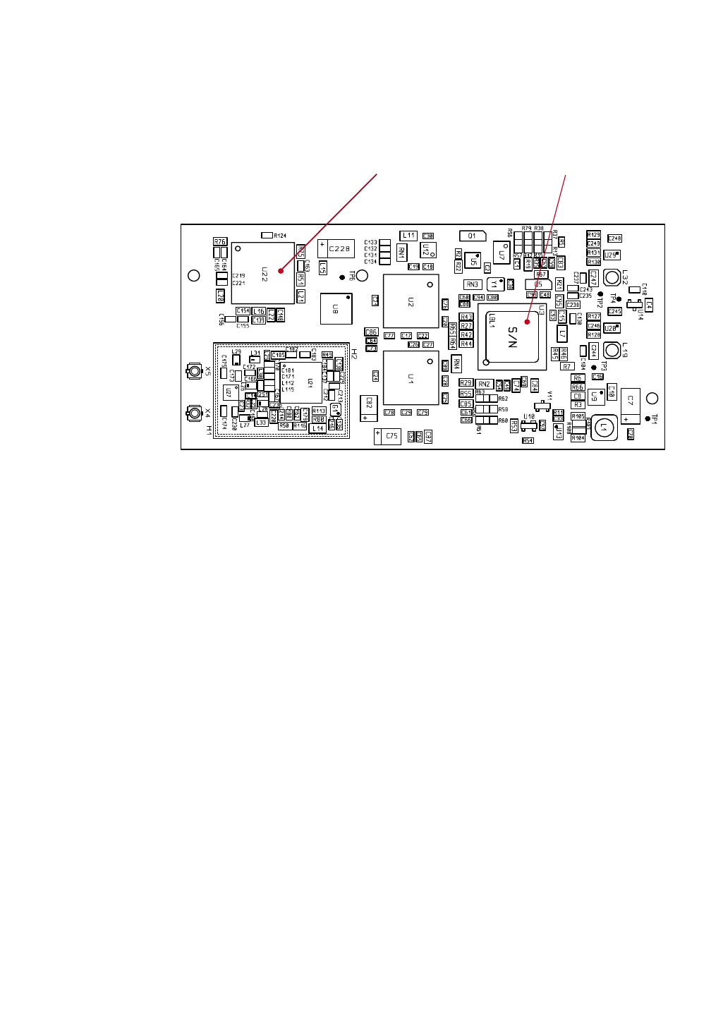
. . . . .
www.digiembedded.com 132
The maximum component case temperature must remain below the maximum,
measured at the devices shown in the figure below.
When attaching thermocouples, please follow the guidelines listed below:
Carefully remove any labels or other foreign material from the component.
Ensure an adhesive with high thermal conductivity is used. Use as little
adhesive as possible.
Make sure the thermocouple is touching the case of the component and not
"floating" in the adhesive.
The use of precision, fine-wire K-type thermocouples is strongly
recommended.
–Omega Engineering P/N 5TC-TT-K-36-72, or similar
recommendations management in applications with operating temperatures at the high end or beyond
the specified standard ambient temperature range.
Providing air movement will improve heat dissipation.
The host PCB plays a large part in dissipating the heat generated by the
module. A large copper plane located on the host ground PCB will improve the
heat dissipation capabilities of the PCB.
Measure Tcase of U22 Measure Tcase of U3
133 ConnectCore 9M 2443 & Wi-9M 2443 Hardware Reference
Appendix B
If the design allows, added buried PCB planes will also improve heat dissipation.
The copper planes create a larger surface to spread the heat into the surrounding
environment.
. . . . . . . . . . . . . . . . . . . . . . . . . . . . . . . . . . . . . . . . . . . . . . . . . . . . . . . . . . . . . . . . . . . . . . . . . . . . . . . . . .
Power requirements
. . . . . . . . . . . . . . . . . . . . . . . . . . . . . . . . . . . . . . . . . . . . . . . . . . . . . . . . . . . . . . . . . . . . . . . . . . . . . . . . . .
Typical Power Requirements
ConnectCore 9M
2443
Parameter ConnectCore 9M 2443 ConnectCore Wi-9M 2443
Input voltage (VLIO
/+3.3V)
3.3V±5% (3.14V to 3.46V) 3.3V±5% (3.14V to 3.46V)
Input current
IVLIO+I+3.3V
554mA max 1.2A max
Input low voltage 0.0V+3.3V<VIL <0.3*V+3.3V 0.0V+3.3V<VIL <0.3*V+3.3V
Input high voltage 0.7*V+3.3V<VIH <V+3.3V 0.7*V+3.3V<VIH <V+3.3V
Output low voltage 0.0V+3.3V <VOL <0.4V+3.3V 0.0V+3.3V <VOL <0.4V+3.3V
Output high voltage V+3.3V-0.4V <VOH <V+3.3V V+3.3V-0.4V <VOH <V+3.3V
533MHz 400MHz
Module State VLIO +3.3V Typical
Power
VLIO +3.3V Typical
Power
U-Boot 142mA 168mA 1023mW 147mA 168mA 1040mW
Windows CE 112mA 167mA 921mW 129mA 165mA 971mW
Ethernet Reset 120mA 70mA 627mW 129mA 70mA 657mW
Suspend 26mA 27mA 175mW 30mA 26mA 185mW

. . . . .
www.digiembedded.com 134
Note: The higher VLIO current of 400 MHz variant due to speed grade specific
S3C2443 PLL voltage requirements.
U-Boot
–U-Boot idle; waiting for serial input
–100 Mbit Ethernet connection idle
–All peripherals provided with clock signals, but not initialized
Windows Embedded CE
–Windows Embedded CE idle
–100 Mbit Ethernet connection idle
–All peripherals except camera and sound provided with clock signals and
initialized
Ethernet Reset
–Windows Embedded CE idle
–100 Mbit Ethernet connection idle
–All peripherals except camera and sound provided with clock signals and
initialized
–Ethernet controller held in reset (GPIO GPA13/ETH_RST# low)
Suspend (CPU in SLEEP mode)
–Windows Embedded CE
–Ethernet deactivated
–All peripheral and CPU clocks stopped, all SoC IP blocks deactivated
ConnectCore
“Wi-9M 2443”
533MHz 400MHz
Module State VLIO +3.3V Typical
Power
VLIO +3.3V Typical
Power
U-Boot 197mA 267mA 1532mW 237mA 232mA 1548mW
Windows CE 220mA 284mA 1664mW 222mA 238mA 1518mW
Ethernet Reset 224mA 190mA 1367mW 222mA 142mA 1202mW
Module State VLIO +3.3V Typical
Power
VLIO +3.3V Typical
Power

135 ConnectCore 9M 2443 & Wi-9M 2443 Hardware Reference
Appendix B
Note: The higher VLIO current of 400 MHz variant due to speed grade specific
S3C2443 PLL voltage requirements.
U-Boot
–U-Boot idle; waiting for serial input
–100 Mbit Ethernet connection idle
–All peripherals provided with clock signals, but not initialized
Windows Embedded CE
–Windows Embedded CE idle
–100 Mbit Ethernet connection idle
–All peripherals except camera and sound provided with clock signals and
initialized
Ethernet Reset
–Windows Embedded CE idle
–100 Mbit Ethernet connection idle
–All peripherals except camera and sound provided with clock signals and
initialized
–Ethernet controller held in reset (GPIO GPA13/ETH_RST# low)
Suspend (CPU in SLEEP mode)
–Windows Embedded CE
–Ethernet deactivated
–All peripheral and CPU clocks stopped, all SoC IP blocks deactivated
Wireless Receive
–Wireless interface initialized, receive only
–Windows Embedded CE idle
–100 Mbit Ethernet connection idle
–All peripherals except camera and sound provided with clock signals and
initialized
Suspend 83mA 90mA 571mW 95mA 72mA 552mW
Wireless
Receive
247mA 346mA 1957mW 300mA 352mA 2152mW
Wireless
Transmit
280mA 705mA 3251mW 300mA 673mA 3211mW
533MHz 400MHz
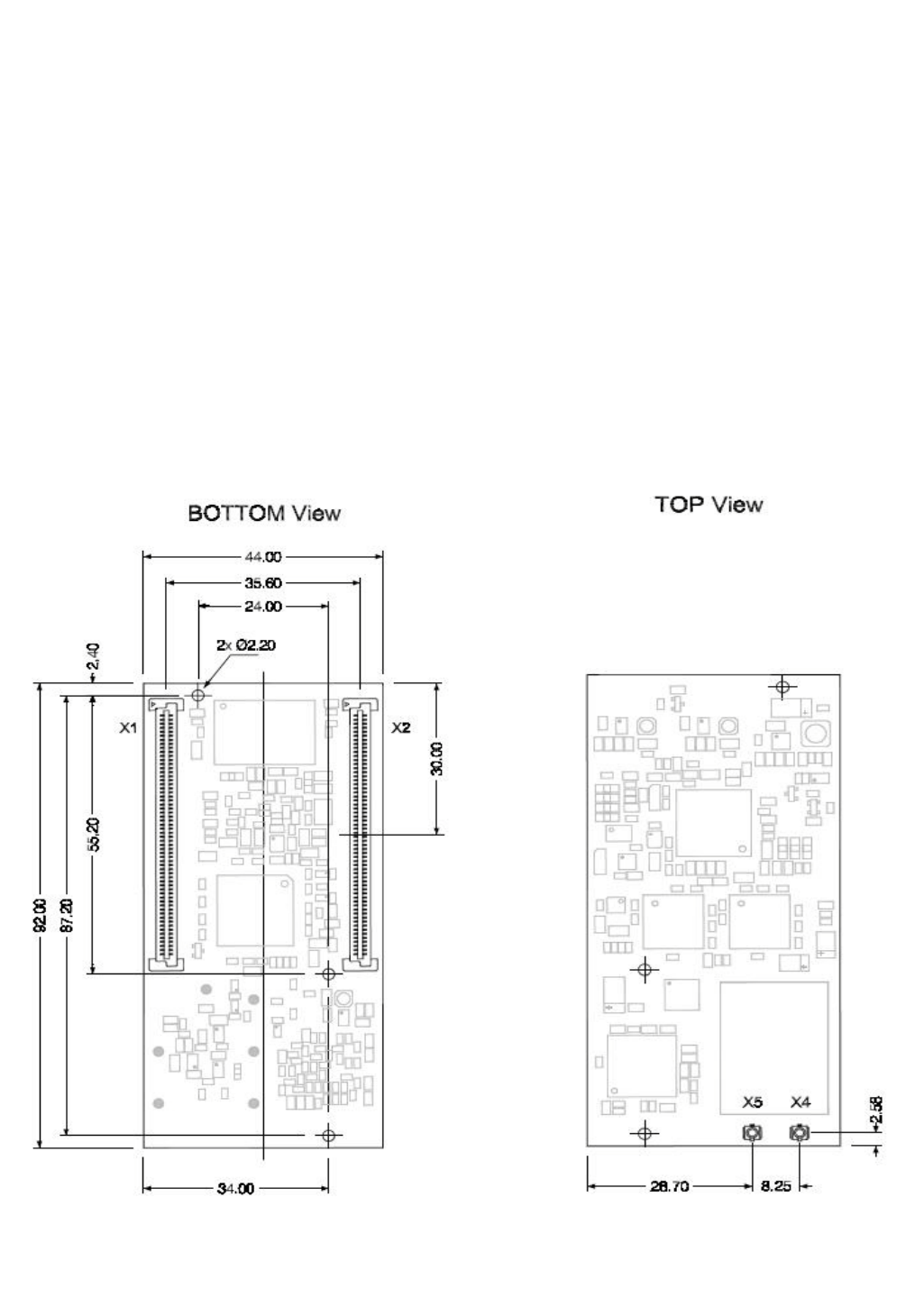
. . . . .
www.digiembedded.com 136
Wireless Transmit
–Wireless interface initialized, continuous transmit (100%)
–Windows Embedded CE idle
–100 Mbit Ethernet connection idle
–All peripherals except camera and sound provided with clock signals and
initialized
. . . . . . . . . . . . . . . . . . . . . . . . . . . . . . . . . . . . . . . . . . . . . . . . . . . . . . . . . . . . . . . . . . . . . . . . . . . . . . . . . .
Mechanical specifications
ConnectCore 9M
2443 Below are the mechanical dimensions of the ConnectCore 9M 2443 Module.
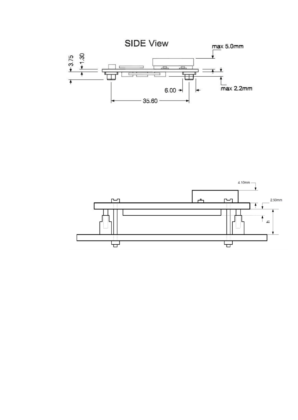
137 ConnectCore 9M 2443 & Wi-9M 2443 Hardware Reference
Appendix B
The module measures 60 x 44mm. Three holes are provided for M2 screws to enable
secure mounting of the module on the base board.
Two board to board connectors are used on the module. The rack-mounted carrier
board has a maximum height from the top of the base board of 13.7mm.
h represents the base board connector height (minimum 5mm) and its value needs to be chosen in
such a way that ensures: 2.5mm + 4.1mm + h ≤ 13.7mm.
See “Connector Reference Parts” table below for further details.
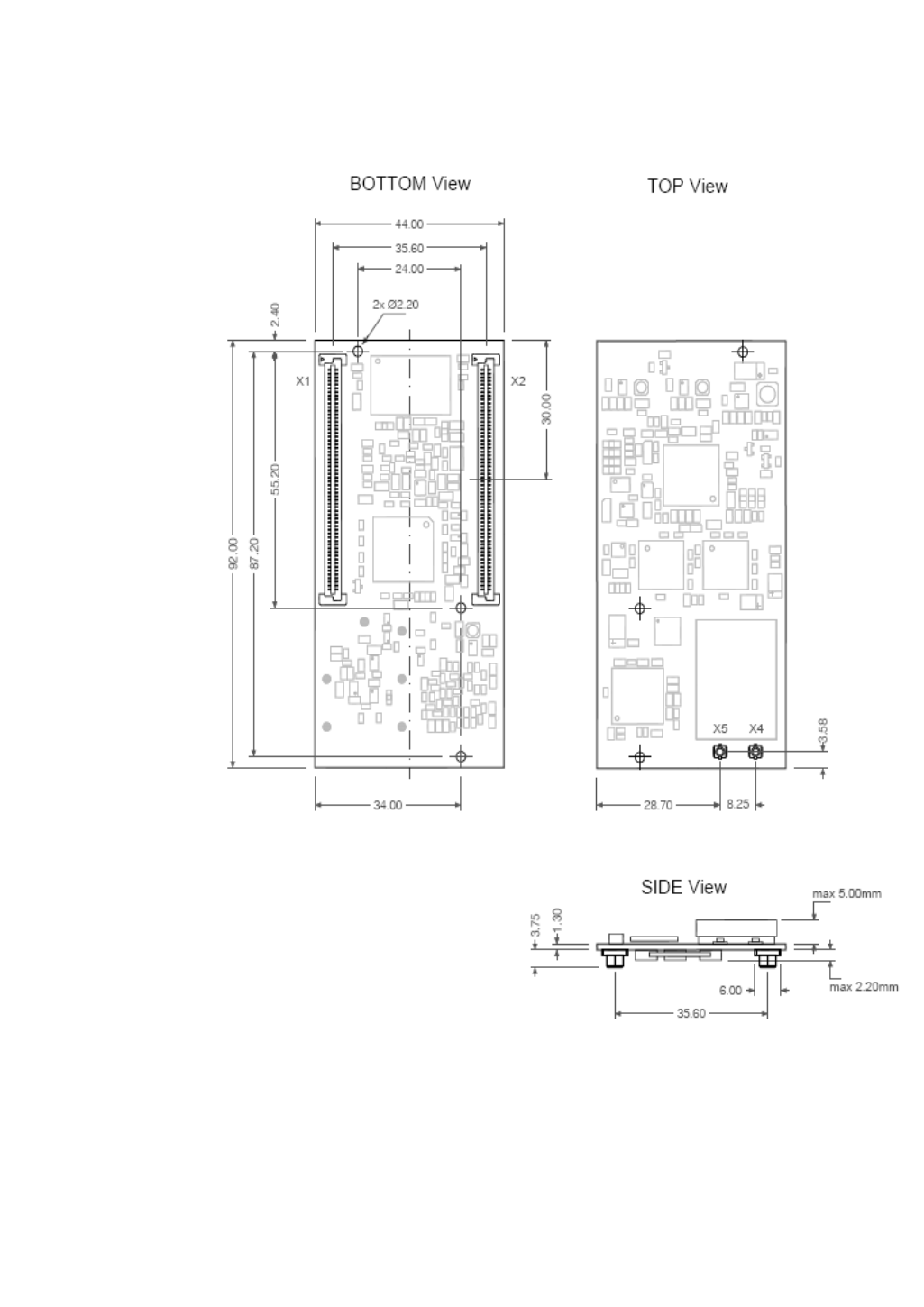
. . . . .
www.digiembedded.com 138
ConnectCore
Wi-9M 2443 The size of the extended module is defined as 92 x 44mm. Three holes for M2
screws are provided to enable secure mounting of the module on the base board.
139 ConnectCore 9M 2443 & Wi-9M 2443 Hardware Reference
Appendix B
. . . . . . . . . . . . . . . . . . . . . . . . . . . . . . . . . . . . . . . . . . . . . . . . . . . . . . . . . . . . . . . . . . . . . . . . . . . . . . . . . .
Connector Reference Parts
Base Board
Connector X1, X2
Base Board
Connector X3, X4
PCB Distance Positions Vendor Manufacturer Part Number
5 mm 120 Tyco 5177984-5
FCI 61083-121000
6 mm 120 Tyco 5179029-5
FCI 61083-122000
7 mm 120 Tyco 5179030-5
FCI 61083-123000
8 mm 120 Tyco 5179031-5
FCI 61083-124000
PCB Distance Positions Vendor Manufacturer Part Number
5 mm 60 Tyco 5177984-5
FCI 61083-061009
6 mm 60 Tyco 5179029-5
FCI 61083-062009
7 mm 60 Tyco 5179030-5
FCI 61083-063009
8 mm 60 Tyco 5179031-5
FCI 61083-064009
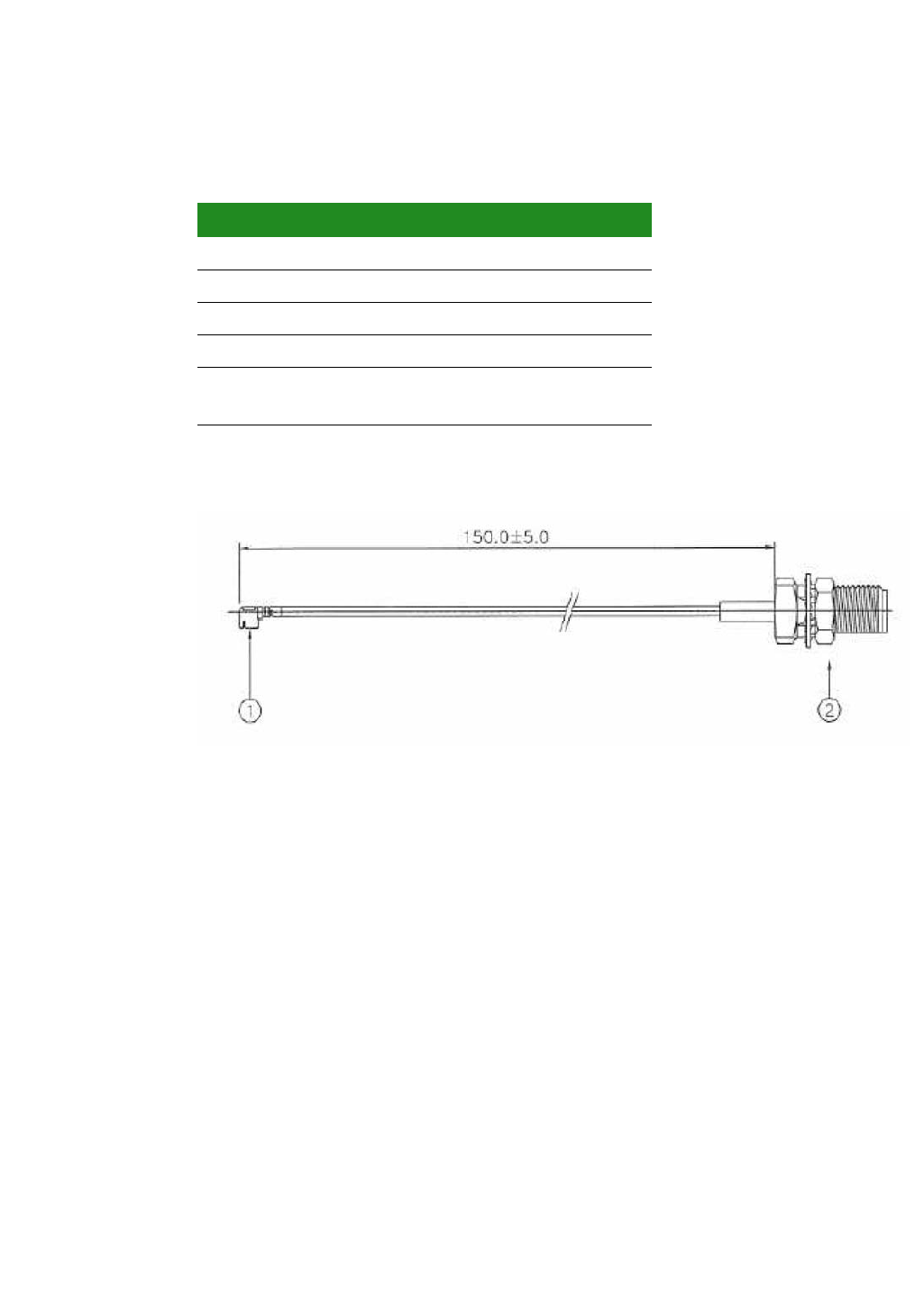
. . . . .
www.digiembedded.com 140
. . . . . . . . . . . . . . . . . . . . . . . . . . . . . . . . . . . . . . . . . . . . . . . . . . . . . . . . . . . . . . . . . . . . . . . . . . . . . . . . . .
Cable specification : U.FL/W.FL to RP-SMA FEMALE
Attributes
Dimensions Note: Dimensions are provided for reference purposes only. The actual cable might
vary.
1 = U.FL
2 = RP-SMA
Note: This module obtained its complete certification by using the cable described
here. End users in North America should use a cable that matches these specs to
maintain the module’s certification.
Attribute Property
Impedance 50 Ohm
Frequency Range 0 to 6 GHz
Length 150 mm /
Temperature Range -40 to +90°C
Loss 3.8dB/m ( 3 GHz )
5.6dB/m ( 6 GHz )
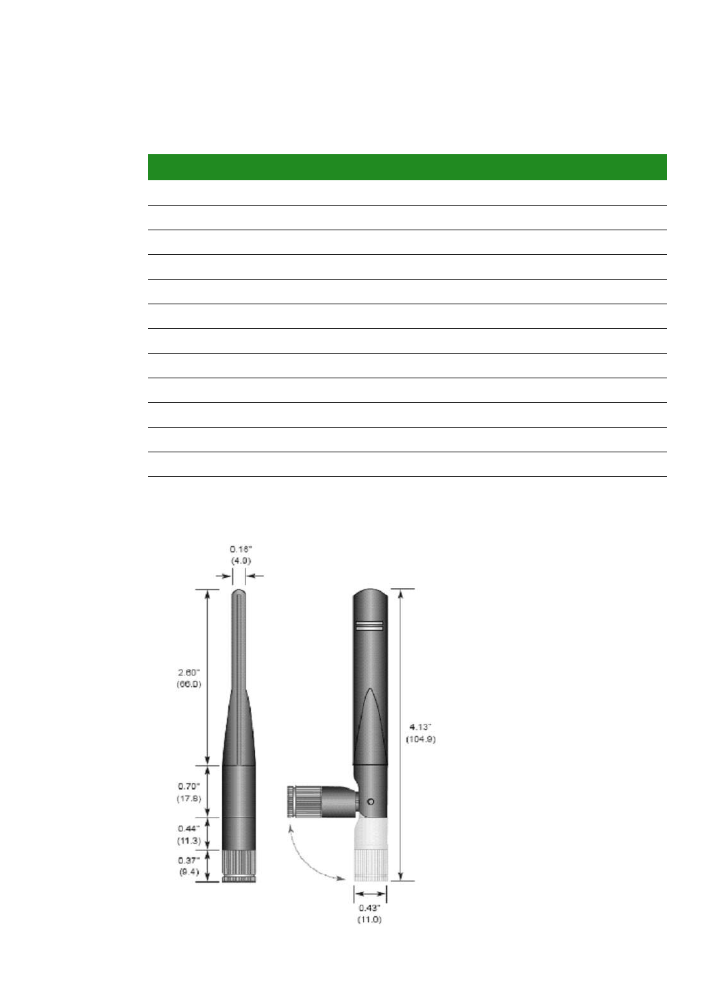
141 ConnectCore 9M 2443 & Wi-9M 2443 Hardware Reference
Appendix B
. . . . . . . . . . . . . . . . . . . . . . . . . . . . . . . . . . . . . . . . . . . . . . . . . . . . . . . . . . . . . . . . . . . . . . . . . . . . . . . . . .
Antenna specification: 802.11a/b/g antenna
Attributes
Dimensions Note: Dimensions are provided for reference purposes only. The actual antenna
might vary.
Attribute Band 1 Band 2
Frequency 2.4~2.483.5GHz 5.15GHz~6GHz
Bandwidth 120MHz 875MHz
Wavelength ¼ Wave ¼ Wave
Impedance 50 Ohm 50 Ohm
VSWR < 1.9 typ. Center < 1.9 typ. Center
Connector RP-SMA RP-SMA
Gain 2.3dBi 3.6dBi
Dimension See measurements in the drawing after the table.
Maximum Power level TBD TBD
Operationg temperature TBD TBD
Storage temperature TBD TBD
Part number ANT-DB1-RAF-RPS
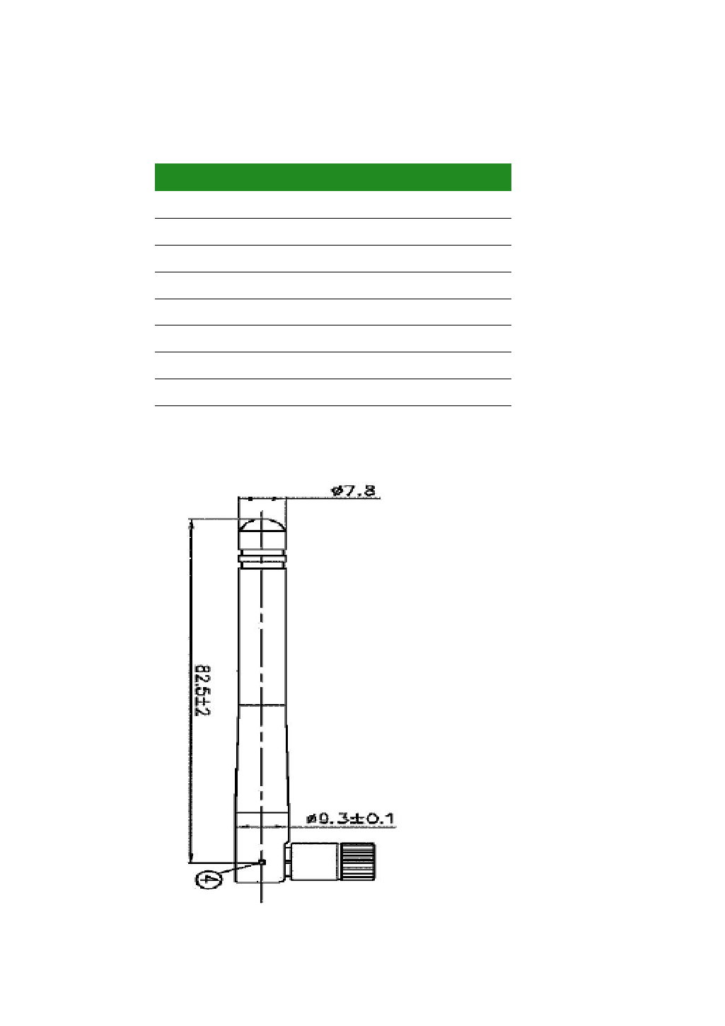
. . . . .
www.digiembedded.com 142
. . . . . . . . . . . . . . . . . . . . . . . . . . . . . . . . . . . . . . . . . . . . . . . . . . . . . . . . . . . . . . . . . . . . . . . . . . . . . . . . . .
Antenna Specification: 802.11b/g antenna
Attributes
Dimensions Note: Dimensions are provided for reference purposes only. The actual antenna
might vary.
Attribute Property
Frequency 2.4~2.5 GHz
Power output 2W
DB gain 2 dBi
VSWR < or = 2.0
Dimension 108.5 mm x 10.0 mm
Weight 10.5g
Temperature rating -40°–+80° C
Part number DG-ANT-20DP-BG
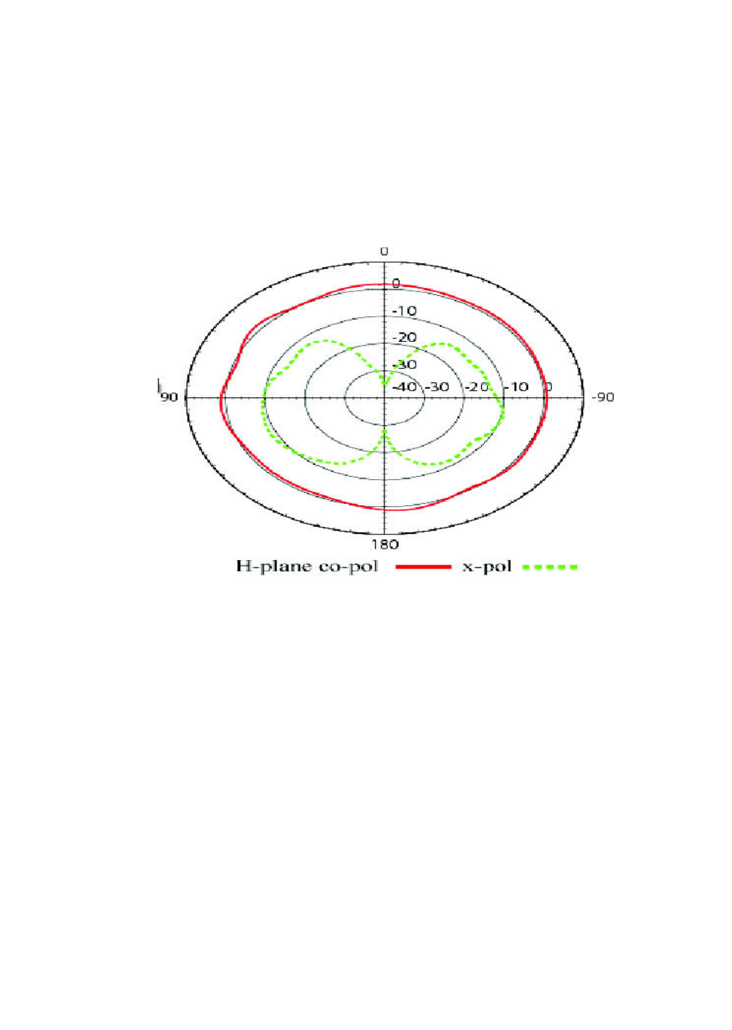
143 ConnectCore 9M 2443 & Wi-9M 2443 Hardware Reference
Appendix B
. . . . . . . . . . . . . . . . . . . . . . . . . . . . . . . . . . . . . . . . . . . . . . . . . . . . . . . . . . . . . . . . . . . . . . . . . . . . . . . . . .
Polar Plots
This diagram shows the strength of the signal received by the whip antenna on both
a horizontal and vertical plane. The diagram shows the magnetic field when the
antenna is in a vertical position. The red solid line represents the horizontal plan
and the green dotted line represents the vertical plane. You can see in the
illustration that at 90 degrees, the signal strength is 0 (as expected).

. . . . .
www.digiembedded.com 144
. . . . . . . . . . . . . . . . . . . . . . . . . . . . . . . . . . . . . . . . . . . . . . . . . . . . . . . . . . . . . . . . . . . . . . . . . . . . . . . . . .
Safety statements
To avoid contact with electrical current:
Never install electrical wiring during an electrical storm.
Use a screwdriver and other tools with insulated handles.
Wear safety glasses or goggles.
Installation of inside wiring may bring you close to electrical wire, conduit,
terminals and other electrical facilities. Extreme caution must be used to avoid
electrical shock from such facilities. Avoid contact with all such facilities.
Protectors and grounding wire placed by the service provider must not be
connected to, removed, or modified by the customer.
Do not touch or move the antenna(s) while the unit is transmitting or receiving.
Do not hold any component containing a radio such that the antenna is very
close to or touching any exposed parts of the body, especially the face or eyes,
while transmitting.
Do not operate a portable transmitter near unshielded blasting caps or in an
explosive environment unless it is a type especially qualified for such use.
Any external communications wiring you may install needs to be constructed to
all relevant electrical codes. In the United States, this is the National Electrical
Code Article 800. Contact a licensed electrician for details.

www.digiembedded.com 145
Appendix B: Certifications
The ConnectCore 9M 2443 and ConnectCore Wi-9M 2443 product complies with
the following standards.
. . . . . . . . . . . . . . . . . . . . . . . . . . . . . . . . . . . . . . . . . . . . . . . . . . . . . . . . . . . . . . . . . . . . . . . . . . . . . . . . . .
FCC Part 15 Class B
Radio Frequency Interface (RFI) (FCC 15.105)
The ConnectCore 9M 2443 module has been tested and found to comply with the
limits for Class B digital devices pursuant to Part 15 Subpart B, of the FCC rules.
These limits are designed to provide reasonable protection against harmful
interference in a residential environment. This equipment generates, uses, and can
radiate radio frequency energy, and if not installed and used in accordance with the
instruction manual, may cause harmful interference to radio communications.
However, there is no guarantee that interference will not occur in a particular
installation. If this equipment does cause harmful interference to radio or television
reception, which can be determined by turning the equipment off and on, the user
is encouraged to try and correct the interference by one or more of the following
measures:
Reorient or relocate the receiving antenna.
Increase the separation between the equipment and receiver.
Connect the equipment into an outlet on a circuit different from that to which
the receiver is connected.
Consult the dealer or an experienced radio/TV technician for help.
Labeling Requirements (FCC 15.19)
This device complies with Part 15 of FCC rules. Operation is subject to the following
two conditions: (1) this device may not cause harmful interference, and (2) this
device must accept any interference received, including interference that may
cause undesired operation.
If the FCC ID is not visible when installed inside another device, then the outside of
the device into which the module is installed must also display a label referring to
the enclosed module FCC ID. THis exterior label can use wording such as the
following: “Contains Transmitter Module FCC ID: MCQ-50M1663/ IC: 1846A-
50M1663”.

146 ConnectCore 9M 2443 & Wi-9M 2443 Hardware Reference
Appendix B
RF Exposure
RF Exposure considerations require that a 20 cm separation distance between users
and the installed antenna location shall be maintained at all times when the module
is energized. OEM installers must consider suitable module and antenna installation
locations in order to assure this in 20cm separation, and end users be also be
advised ot the requirement.
Modifications (FCC 15.21)
Changes or modifications to this equipment not expressly approved by Digi may void
the user’s authority to operate this equipment.
Industry Canada
This digital apparatus does not exceed the Class B limits for radio noise emissions
from digital apparatus set out in the Radio Interference Regulations of the Canadian
Department of Communications.
Le present appareil numerique n’emet pas de bruits radioelectriques depassant les
limites applicables aux appareils numeriques de la class B prescrites dans le
Reglement sur le brouillage radioelectrique edicte par le ministere des
Communications du Canada.
The maximum antenna gain permitted in the bands 5250-5350 MHz and 5470-5725
MHz to comply with the e.i.r.p limit is, according to RSS-210 section A9.2(2)
250mW conducted power
1.0W max EIRP
This limit is met with the highest gain antenna listed,antennafactor
ANT-DB1-RAF-RPS.
The maximum antenna gain permitted in the band 5725-5825 MHz to comply with
the e.i.r.p limit specified for non point-to-point operation is,according to RSS-210
section A9.2(3):
1W conducted power
4.0W max EIRP
This limit is met with the highest gain antenna listed,antennafactor
ANT-DB1-RAF-RPS.

. . . . .
www.digiembedded.com 147
OEM installers and users are cautioned to take note that high-power radars are
allocated as primary users (meaning they have priority) of the bands 5250-5330 MHz
and 5650-5850 MHz and these radars could cause interference and /or damage to
devices operating in these frequency bands.
Indoor/Outdoor
When the ConnectCore W9M2443 module is installed in devices that can be used
outdoors, the channels in the band 5150-5250 MHz must be disabled to comply with
US and Canadian regulatory requirements. The OEM users are encouraged to inform
end users of this restriction as well.

148 ConnectCore 9M 2443 & Wi-9M 2443 Hardware Reference
Appendix B
Declaration of Conformity
(In accordance with FCC Dockets 96-208 and 95-19)
Digi International declares that the product:
to which this declaration relates, meets the requirements specified by the Federal
Communications Commission as detailed in the following specifications:
Part 15, Subpart B, for Class B equipment
FCC Docket 96-208 as it applies to Class B personal
Personal computers and peripherals
The product listed above has been tested at an External Test Laboratory certified
per FCC rules and has been found to meet the FCC, Part 15, Class B, Emission
Limits. Documentation is on file and available from the Digi International
Homologation Department.
Manufacturer’s Name: Digi International
Corporate Headquarters: 11001 Bren Road East
Minnetonka MN 55343
Manufacturing Headquarters: 10000 West 76th Street
Eden Prairie MN 55344
Product Name ConnectCore 9M 2443
Model Number: 50001664-xx
. . . . .
www.digiembedded.com 149
International EMC Standards
The ConnectCore 9M 2443 meets the following standards:
Standards ConnectCore 9M 2443
Emissions FCC Part 15 Subpart B
IS-003
Immunity EN 55022
EN 55024
Safety UL 60950-1
CSA C22.2, No. 60950-1
EN60950-1