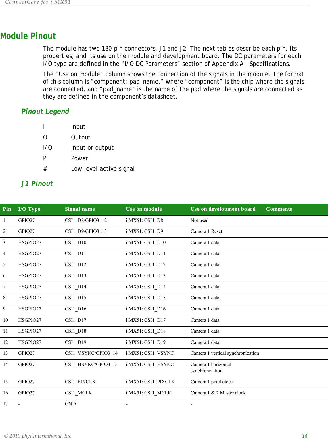
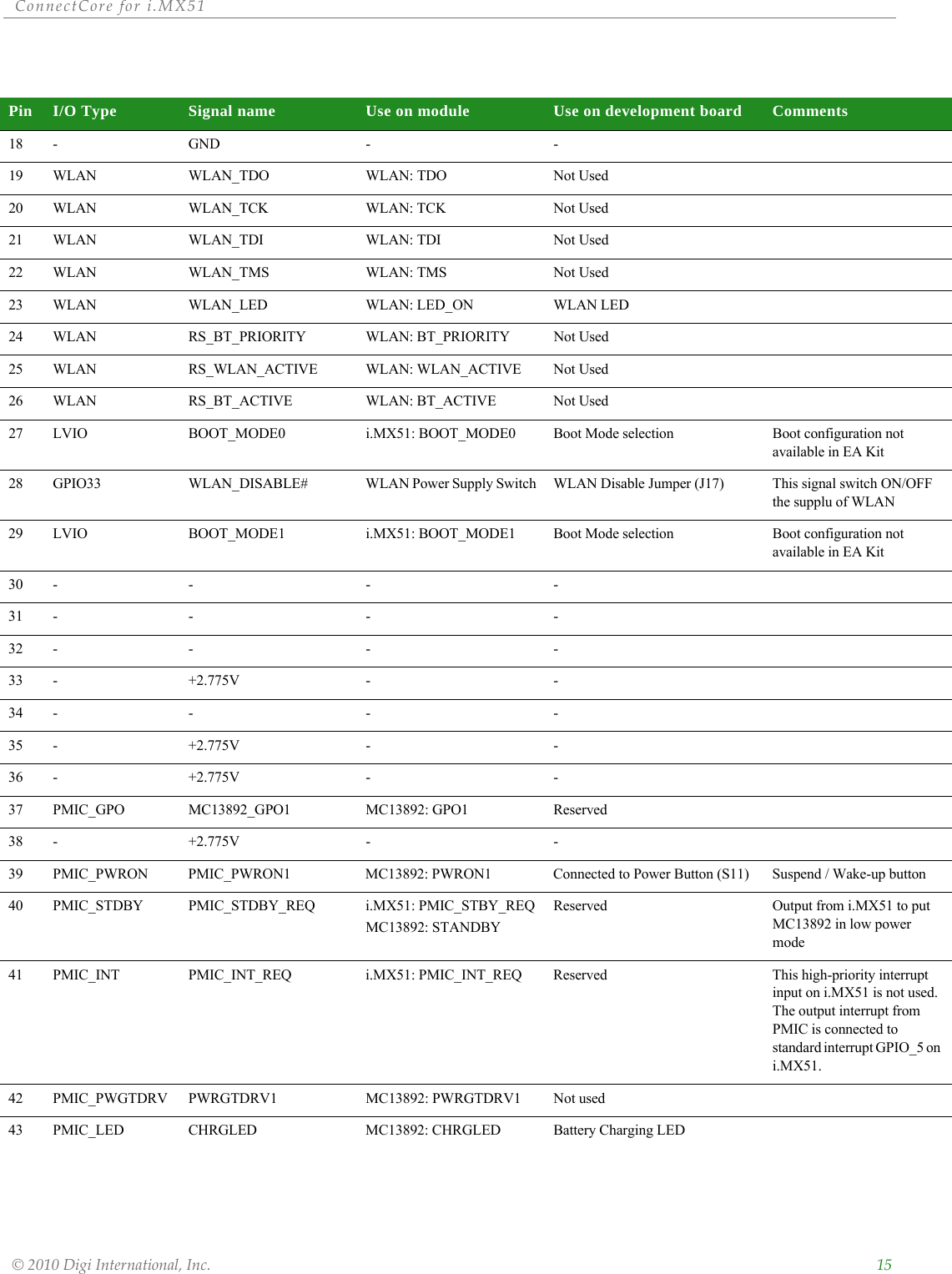
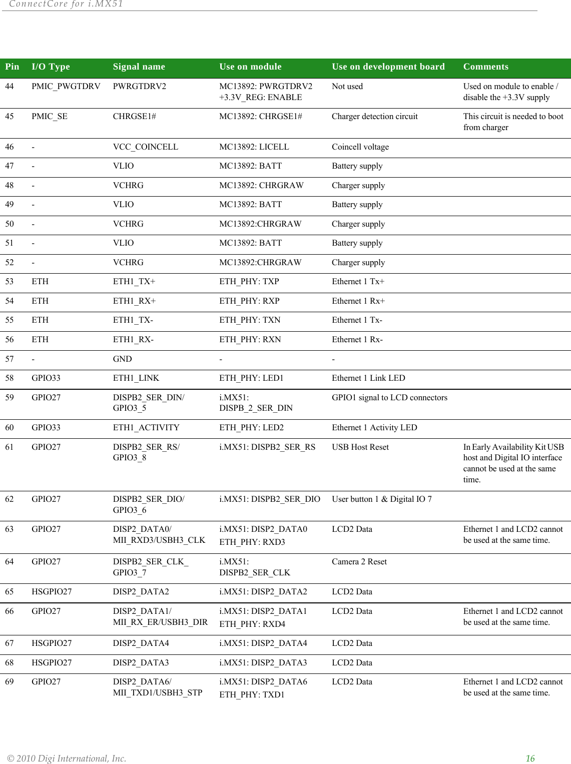
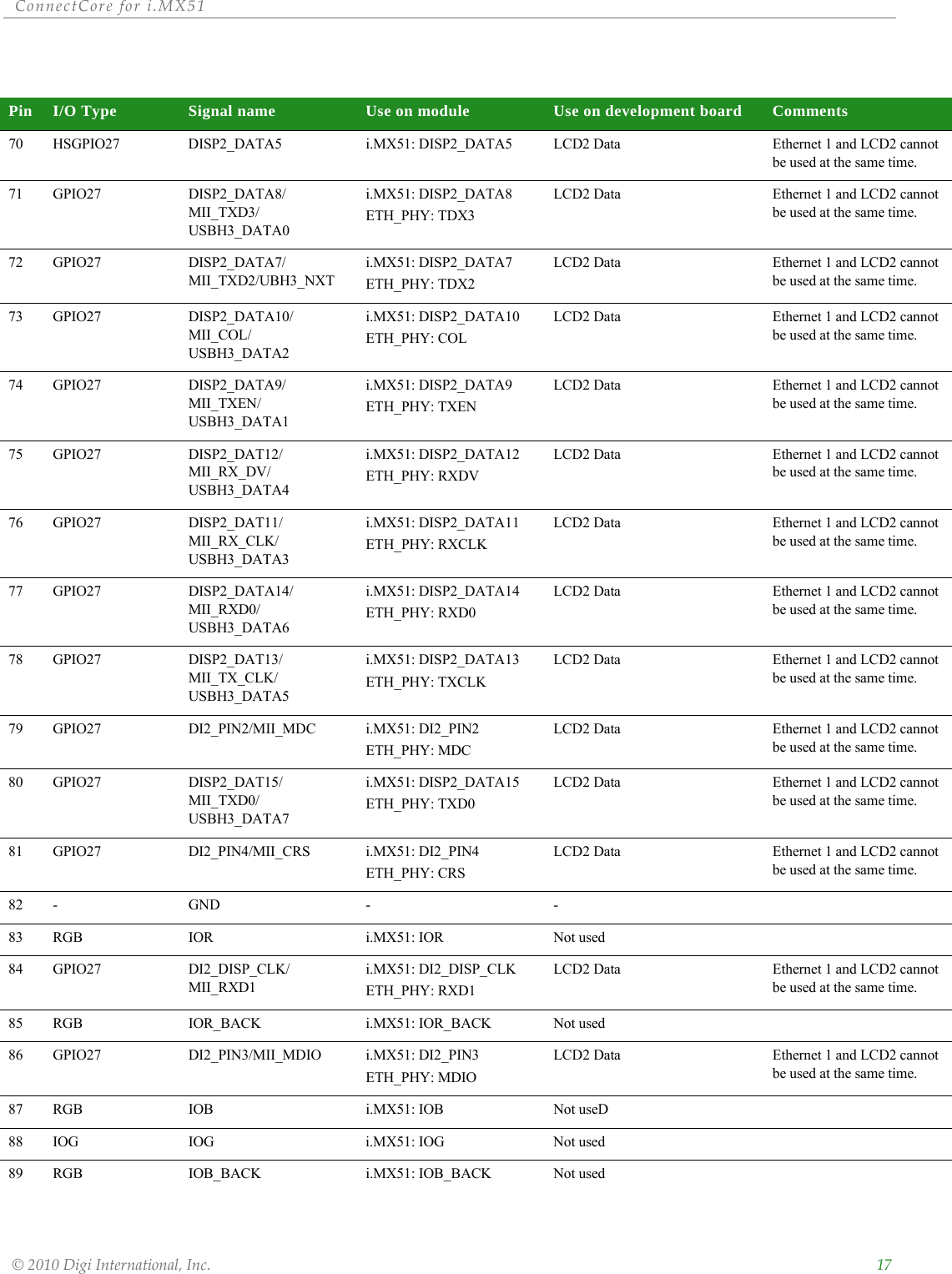
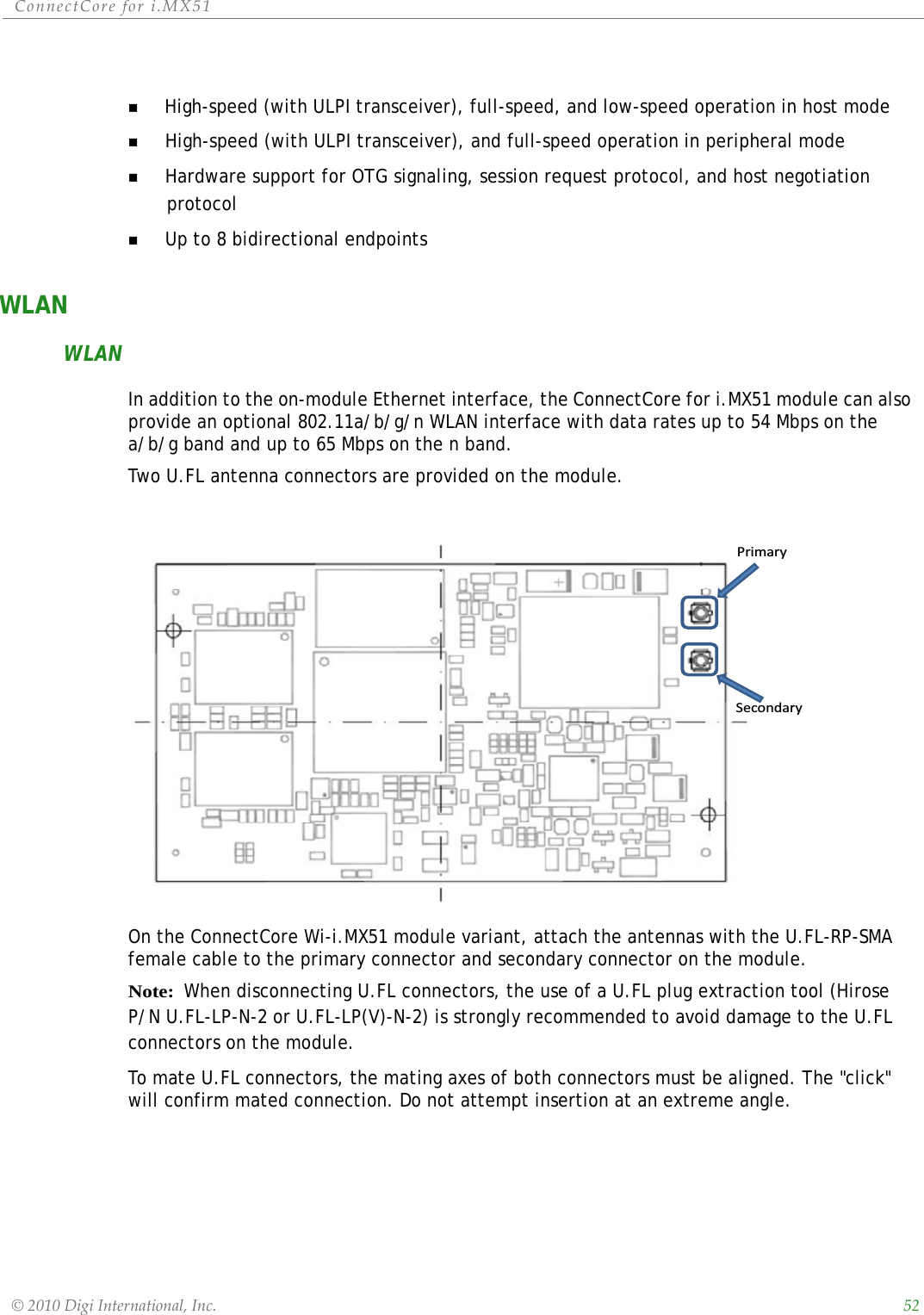
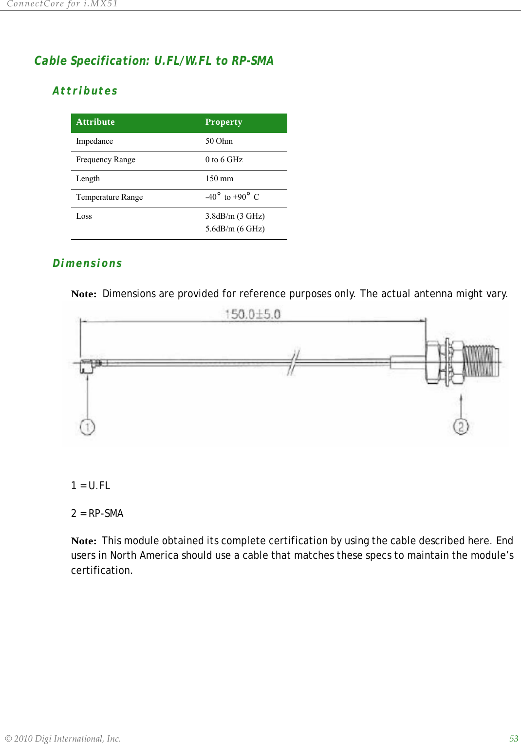
Digi 50M1699 WLAN Module User Manual CC Wi i MX51 HRM
Digi International Inc WLAN Module CC Wi i MX51 HRM
Digi >
Contents
- 1. User Manual Part1
- 2. User Manual Part2
- 3. User Manual Part3
- 4. User Manual Part4
- 5. User Manual
User Manual Part1
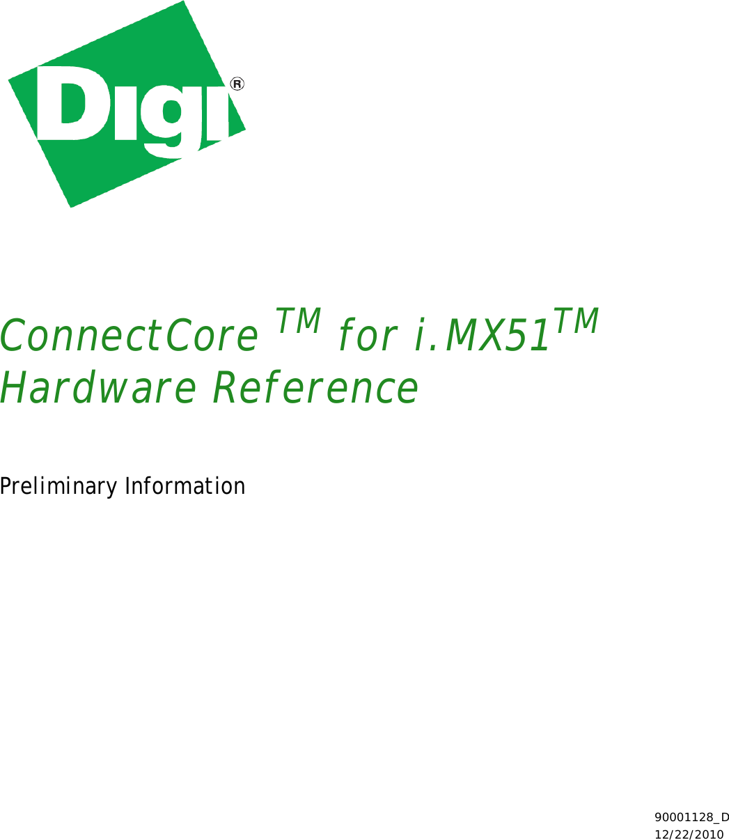

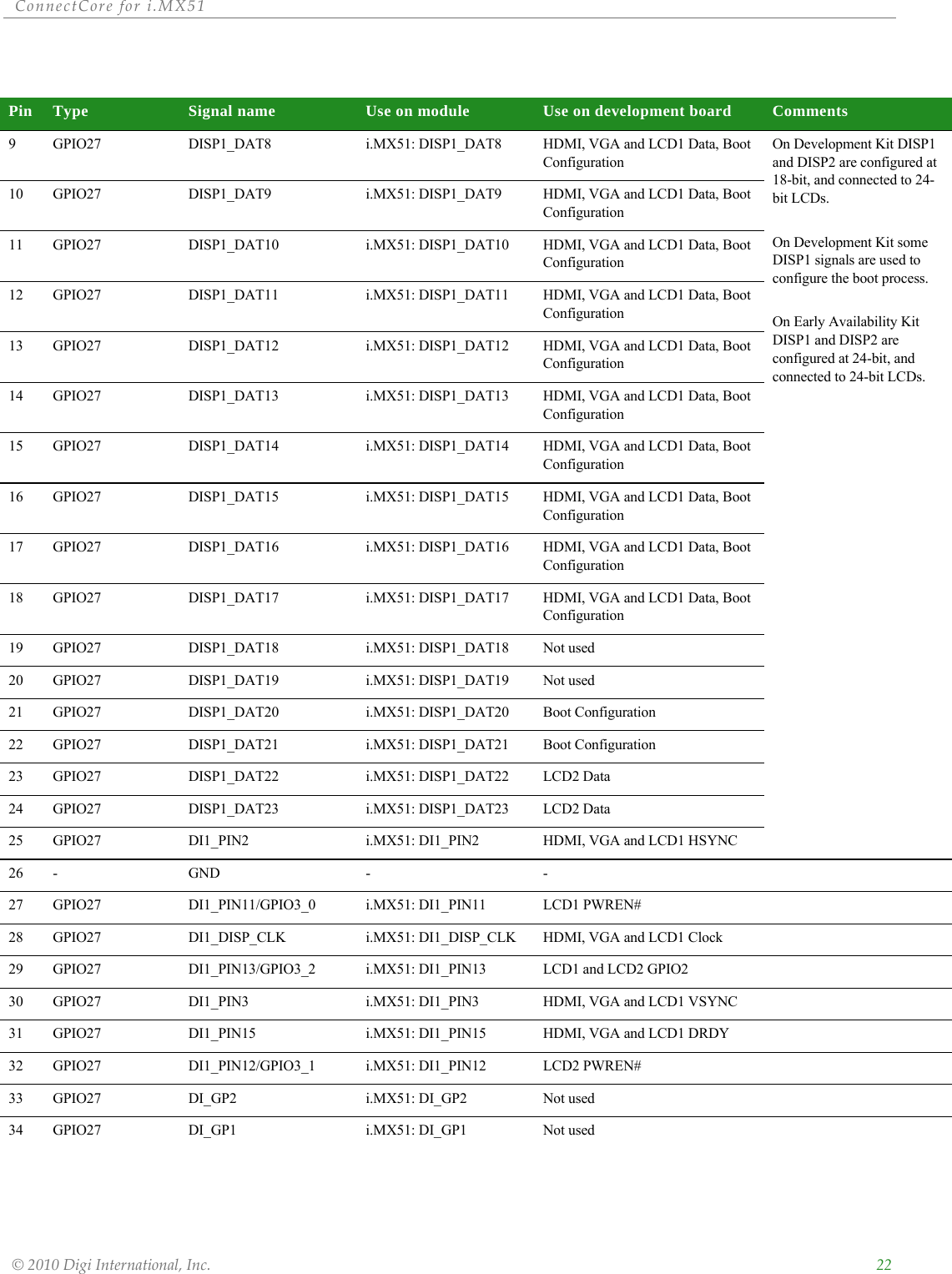
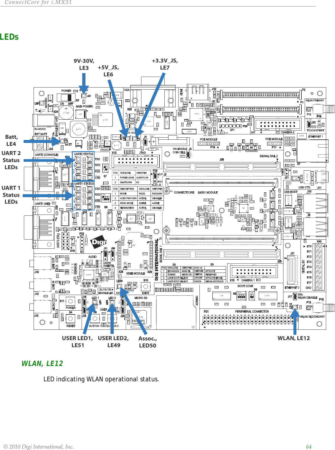
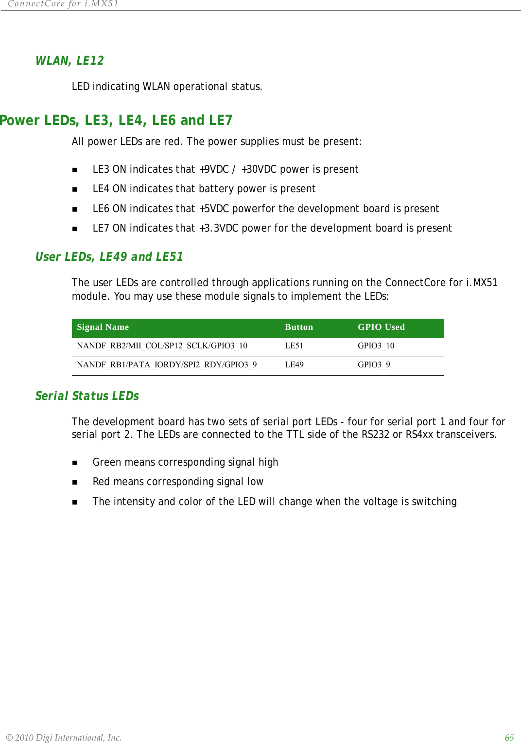
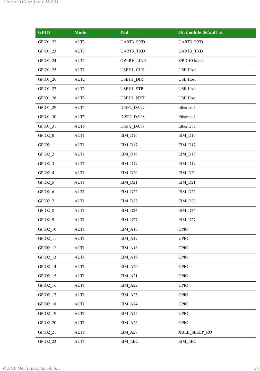
![ConnectCorefori.MX51©2010DigiInternational,Inc. 33Memory DDR2 SDRAM Memory The ConnectCore for i.MX51 module provides up to 512 MBytes of DDR2-400 SDRAM memory. The module can support up to four 16-bit, 128Mbit, DDR2-400 chips, configured as two banks of 32-bits of 128Mbits DDR2-400 memory.NAND Flash MemoryThe ConnectCore for i.MX51 module provides 512Mbytes of NAND-Flash memory. On the module a 512MByte, 2Kbyte page, NAND-Flash chip is used.Options for other densities NAND Flash devices are available depending on the module variant. Chip selects Chip Select Memory MapThe ConnectCore for i.MX51 has eight chip select signals, two for dynamic memory and six for static memory. The table below shows the memory map of these chip select signals.Name Pin Address range Sixe [Mb] Usage CommentsDRAM_CS0# Y4 0x9000_000-0x9FFF_FFFF256M DDR2 bank 0 First bank on moduleDRAM_CS1# Y3 0xA000_0000-0xAFFF_FFFF256M DDR2 bank 1 Second bank on moduleEIM_CS0 W6 0xB000_000-0xB7FF_FFFF128M External CS0#EIM_CS1 Y6 0xB800_000-0xBFFF_FFFF128M External CS1#EIM_CS2 Y7 0xC000_000-0xC7FF_FFFF128M External CS2#EIM_CS3 AC3 0xC800_000-0xCBFF_FFFF64M External CS3#EIM_CS4 AA6 0xCC00_000-0xCDFF_FFFF32M External CS4#EIM_CS5 AA5 0xCE00_000-0xCFFE_FFFF32M (minus 64K) External CS5# Used for Ethernet Controller on module](https://usermanual.wiki/Digi/50M1699.User-Manual-Part1/User-Guide-1406129-Page-33.png)
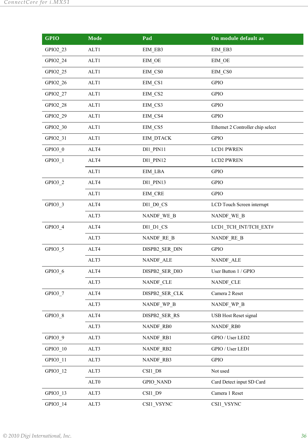
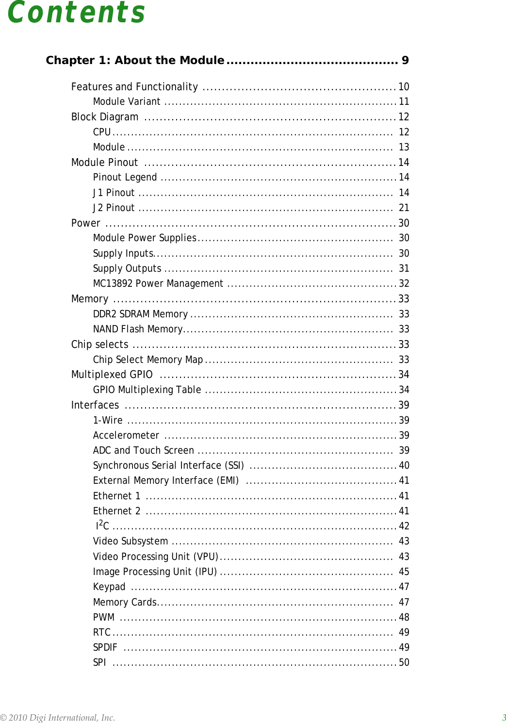
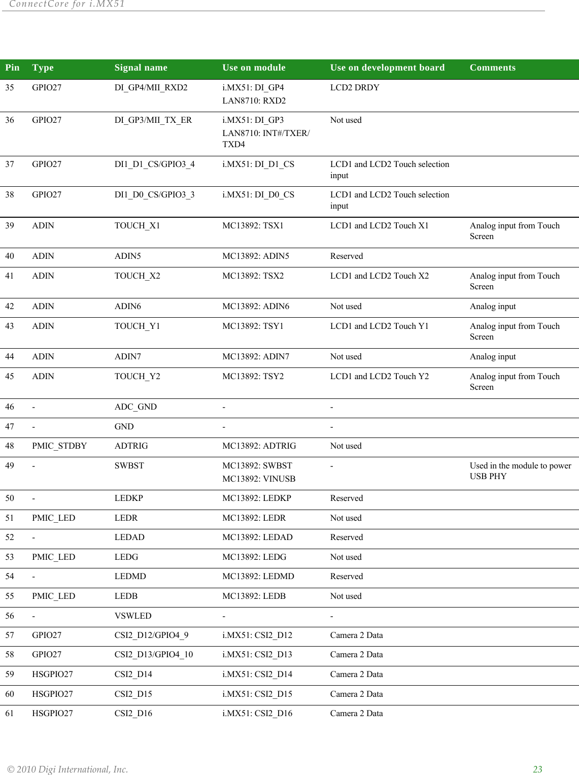
![ConnectCorefori.MX51©2010DigiInternational,Inc. 41External Memory Interface (EMI)The module provides access to the external memory controller. This memory controller handles the interface to devices external to the chip, including generation of chip selects, clock and control for external peripherals and memory. It provides asynchronous access to devices with SRAM-like interface and synchronous access to devices with NOR Flash like or PSRAM like interfaces.The following lines of the memory controller are available in the module connectors:Support for multiplexed address/data bus operations X16 and X32Programmable data port size of each Chip select (X8, X16 and X32)28-but address busUp to 5 Chip selectsRead and write control lines2 x byte enable signalsRegister/command selection line (CRE)Note: from Freescale: 8-bit memory devices are supported by EMI interfaces connecting to only one of the followign three locations:EIM_DA[7:0] padsEIM_DA[15:8] padsEIM_DA[31:24] padsConection to the EIM_D[23:16] pads is not supported.Ethernet 1The ConnectCore for i.MX51 provides a Fast Ethernet Controller (FEC) designed to support both 10 and 100 Mbps Ethernet/IEEE 802.3 networks. A low power consumption 10/100 Ethernet transceiver (LAN8710A) from SMSC is used on the module to complete the interface to the media.The module does not provide a transformer and Ethernet connector. The PHY address on the MII bus is 0x7 (0b00111).The module also provides two status signals for activity and link LEDs.Ethernet 2 The ConnectCore for i.MX51 module can provide a high-performance 10/100Mbit Ethernet controller (LAN9221) with integrated MAC and PHY from SMSC as a second Ethernet port.The main features of this Ethernet controller are the following:Embedded 16 Kbyte FIFO for packet buffers](https://usermanual.wiki/Digi/50M1699.User-Manual-Part1/User-Guide-1406129-Page-41.png)

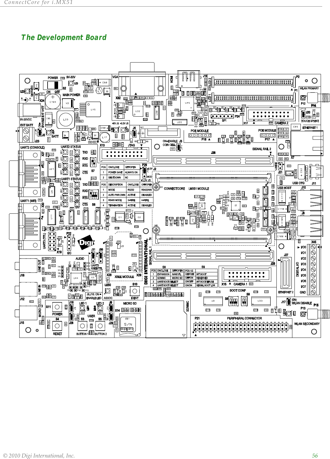
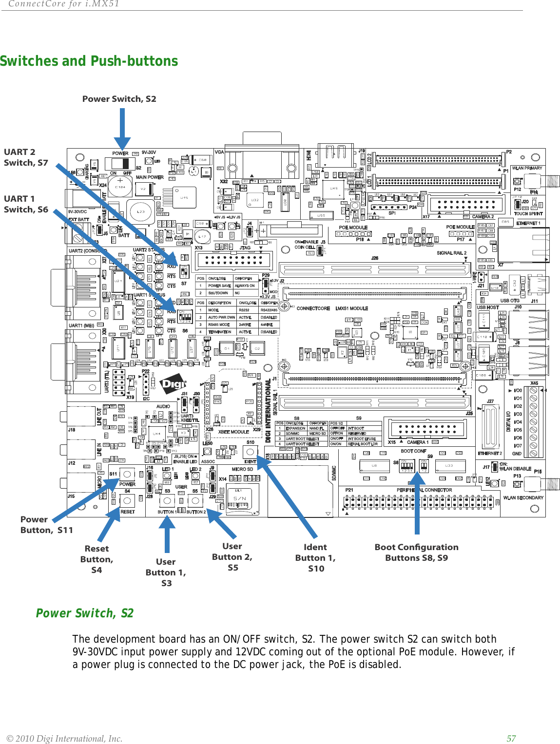
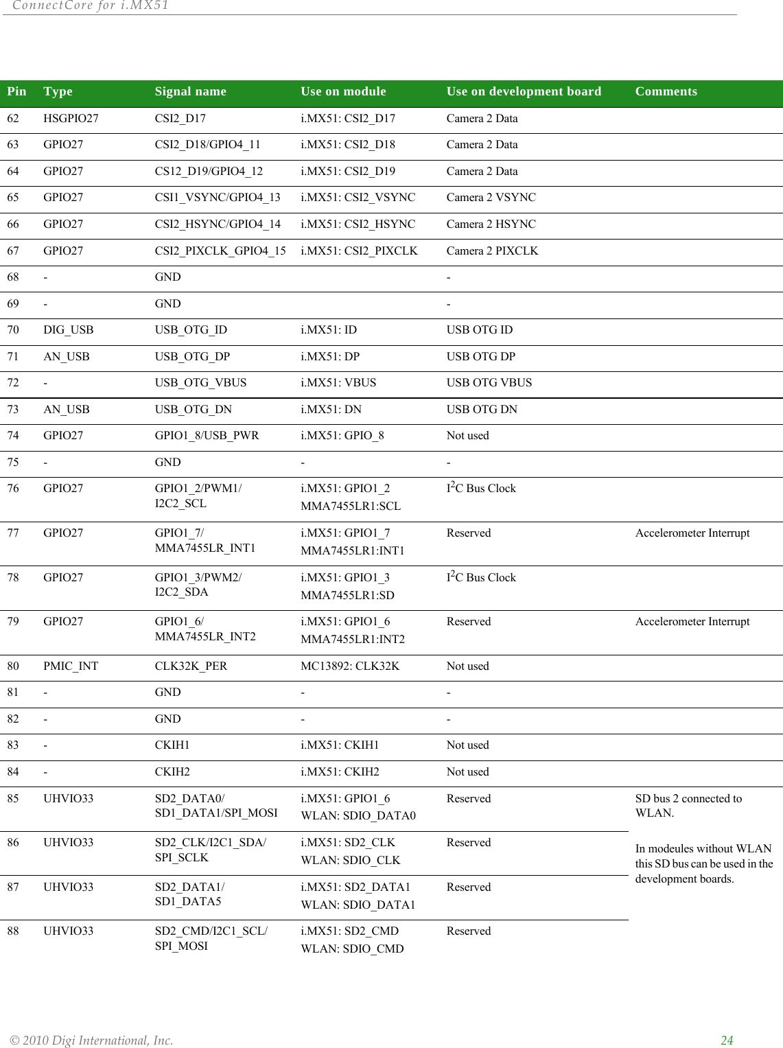
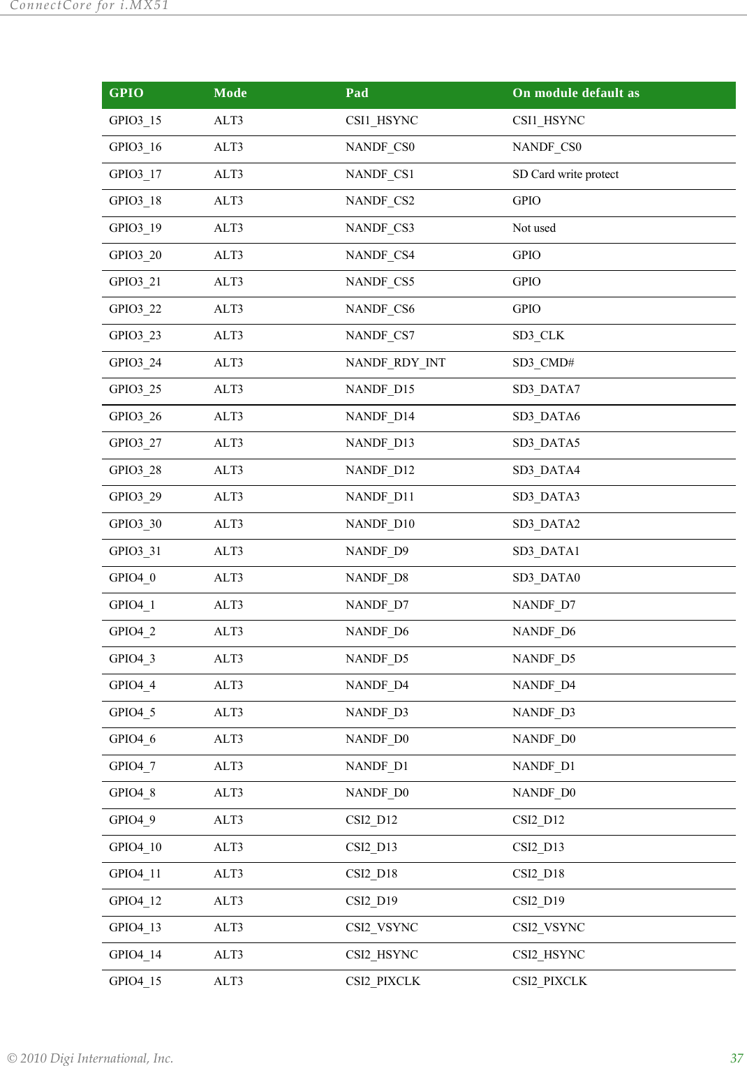
![ConnectCorefori.MX51©2010DigiInternational,Inc. 58Reset Button, S4The reset push-button S4, resets the module and the peripherals on the development board. A push-button allows manual reset by connecting POR# or optionally RSTIN# to ground.Power Button, S11The power button S11, generates a Turn On/Turn Off interrupt to the MC13892 power management device on the module.The Turn Off event does not directly power off the module.The module is powered off by the processor's response to this interrupt. The software can configure a user initiated power down, or a transition to a low power off mode by pressing this power button.When in Off mode or in low power mode, the module can be powered via the Turn On event generated by pressing the Power button.User Buttons, S3 and S5Use the user push-buttons to interact with the applications running on the ConnectCore for i.MX51 module. Use these module signals to implement the push-buttons:GPIO3_6 is used in User Button S3 and also in the Digital I/O connector for Digital I/O7.Ident Button, S10The Ident push-button S10 is associated to the commissioning input of the Digi XBee modules. This input provides a variety of simple functions to aid in deploying devices in a network. For a deeply description of this functionality please refer to the Digi XBee modules documentation.Legend for Multi-Position SwitchesSwitches S6, S7, S8 and S9 are multi-pin switches. In the description tables for these switches, the position is designated as S[switch number].[pin number]. For example, position 1 on switch S6 is specified as S6.1.Signal Name Button GPIO UsedDISPB2_SER_DIO/GPIO3_6/USER_KEY1 S3 GPIO3_8GPIO1_1/SD1_WP#/SPI_MISO/USER_KEY2 S5 GPIO1_1](https://usermanual.wiki/Digi/50M1699.User-Manual-Part1/User-Guide-1406129-Page-58.png)