Digi 50M1745 802.11 b/g/n digital transceiver module User Manual Digi Connect ME and Wi ME Hardware Reference
Digi International Inc 802.11 b/g/n digital transceiver module Digi Connect ME and Wi ME Hardware Reference
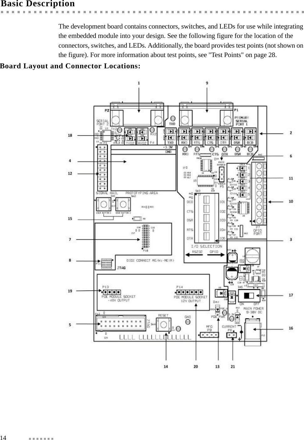
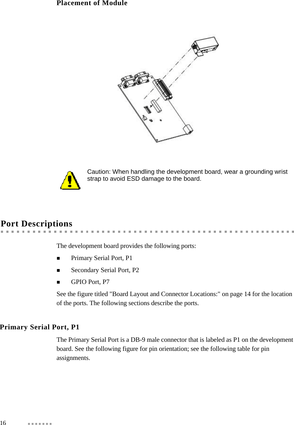
Digi >
Contents
- 1. User Manual 1
- 2. User Manual 2
User Manual 1

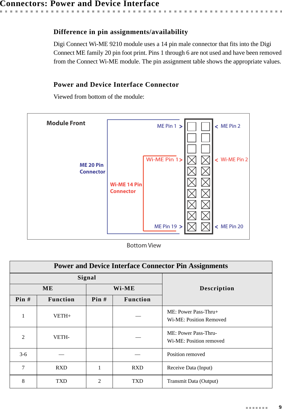
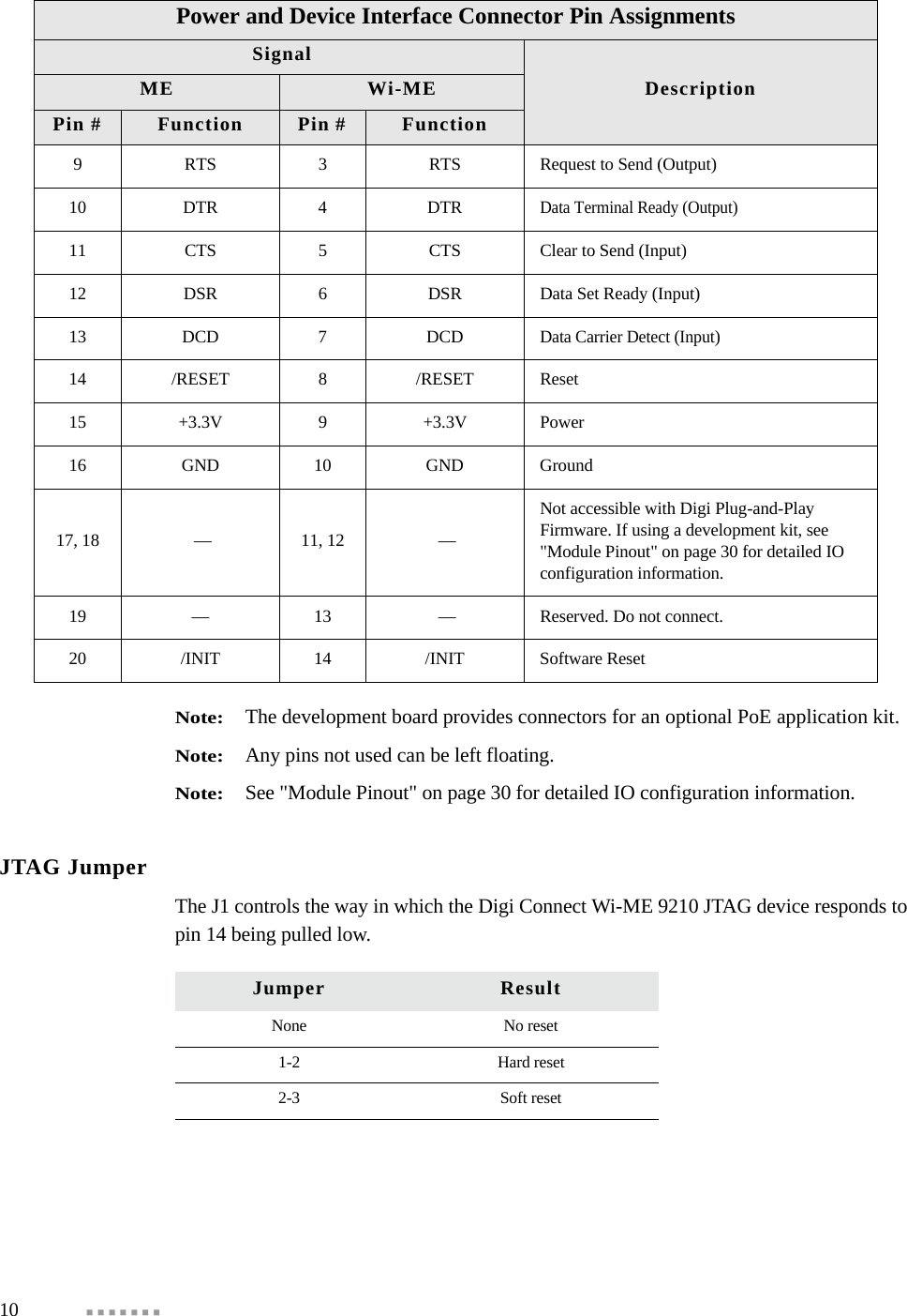
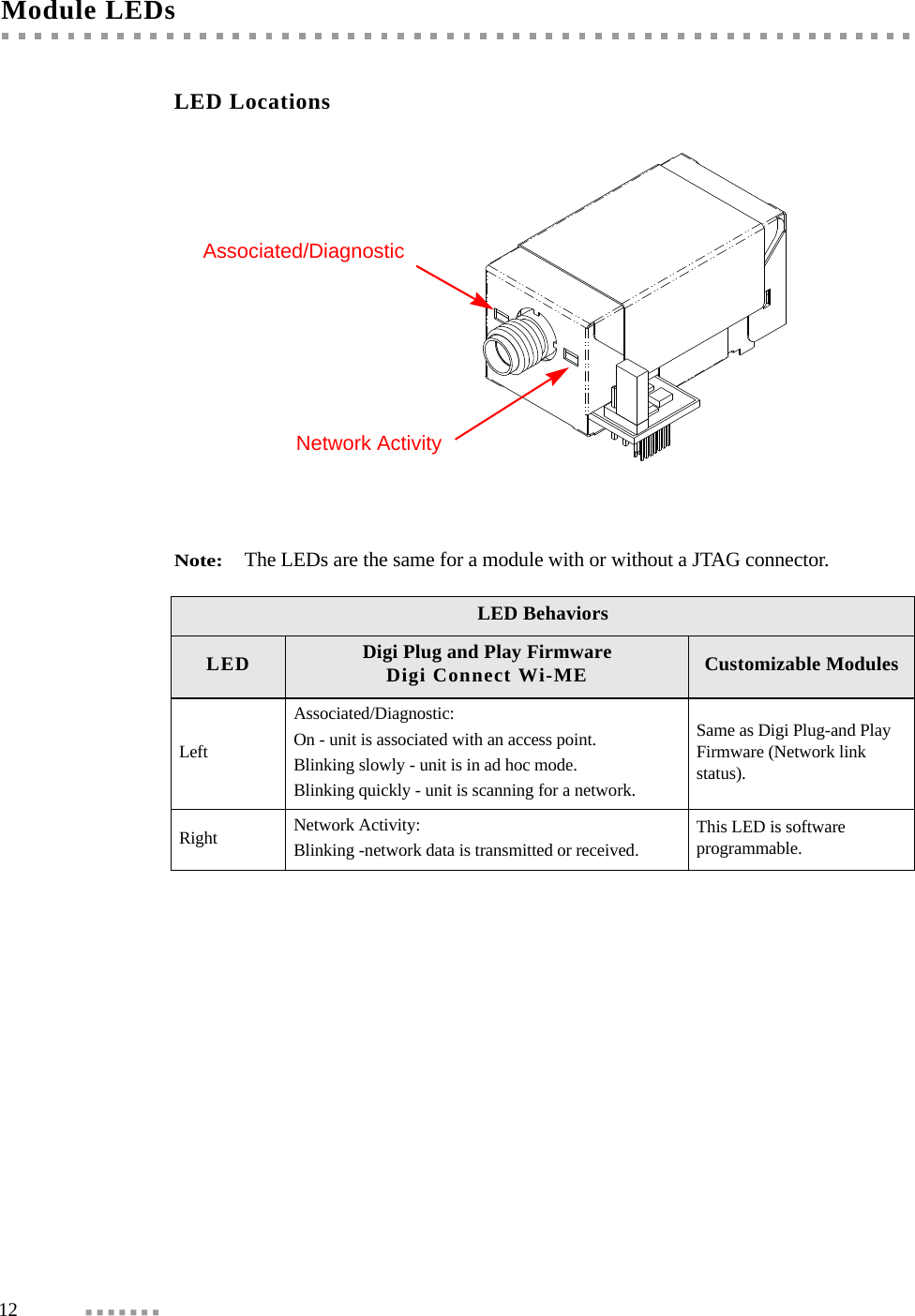
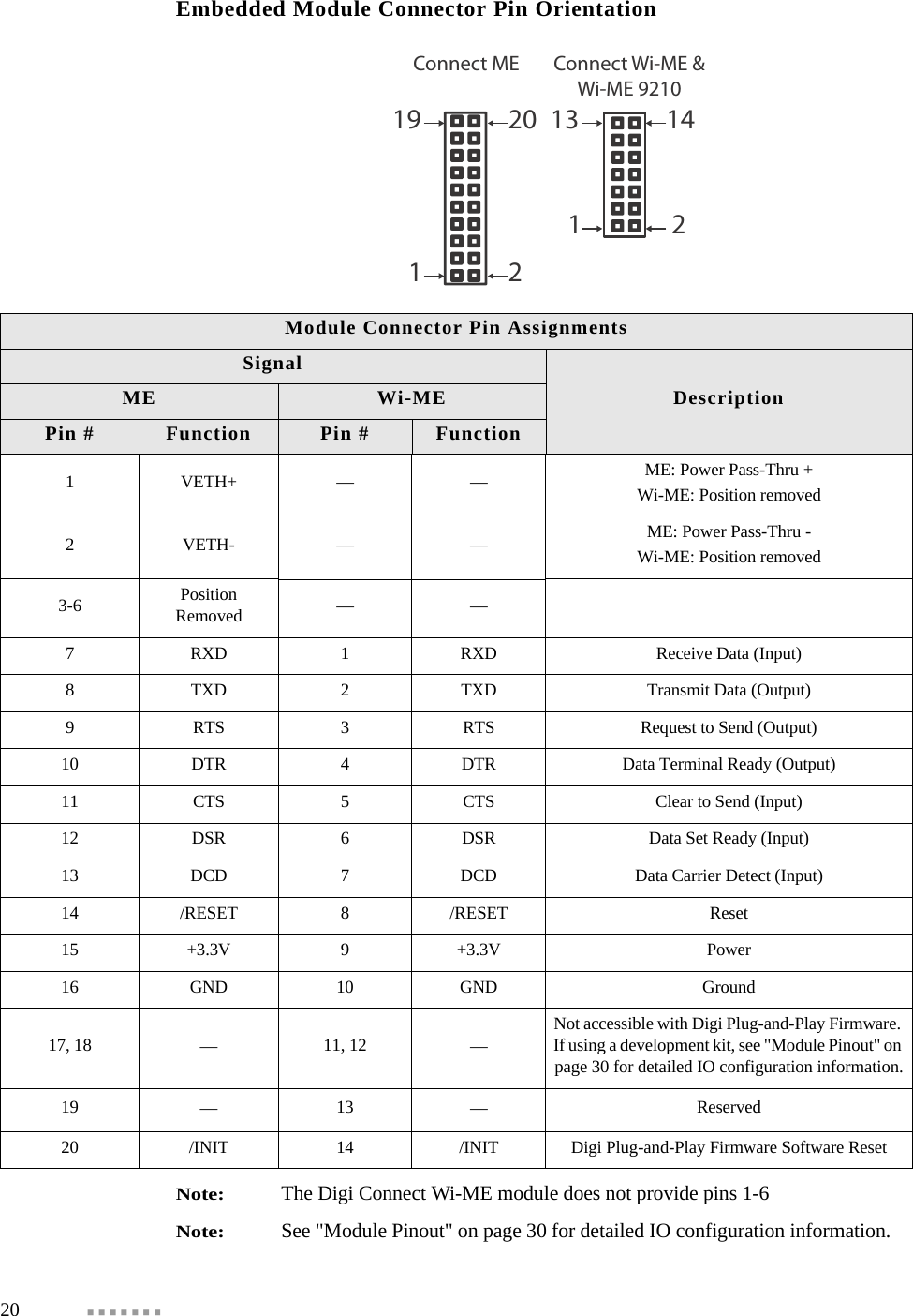
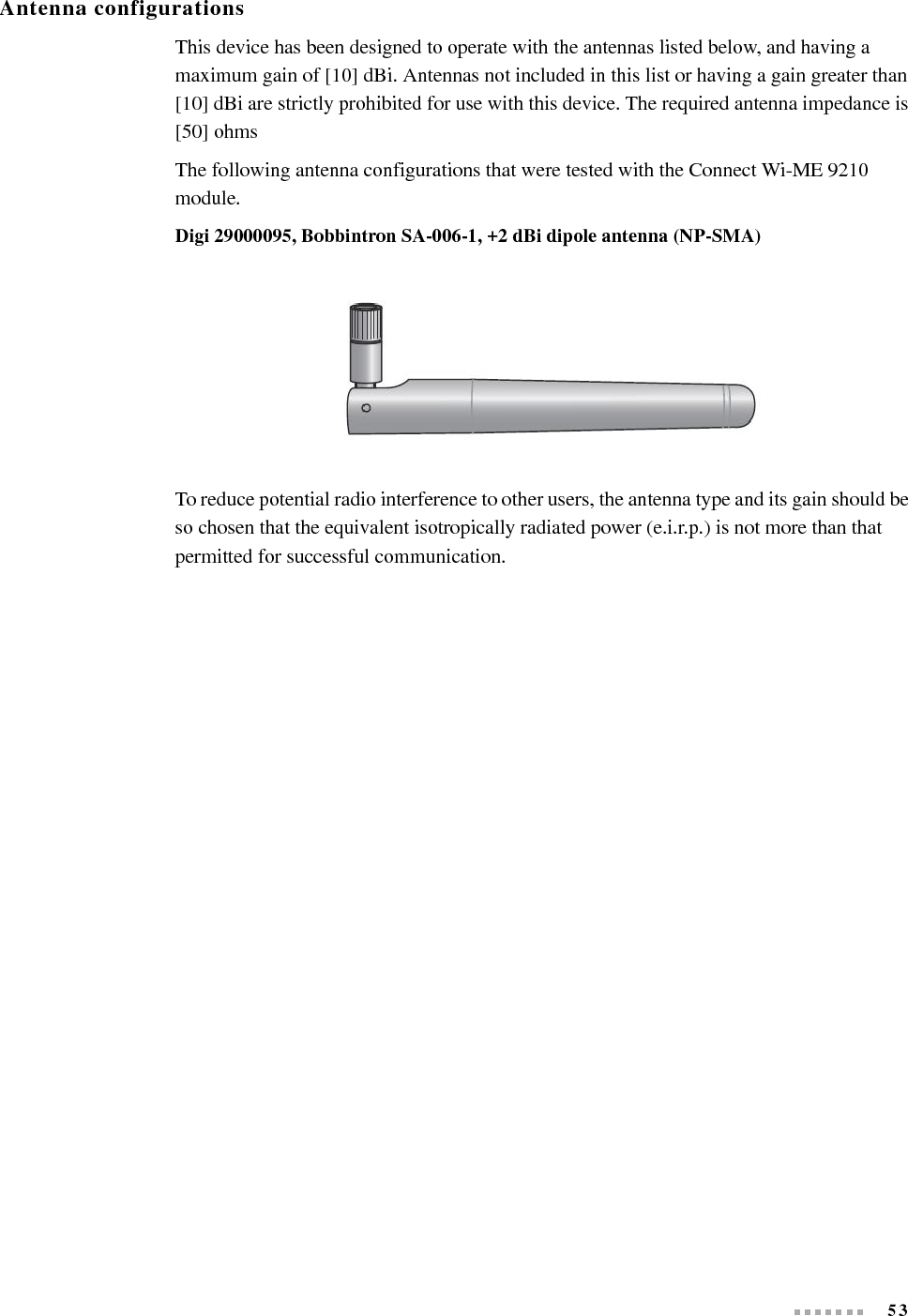
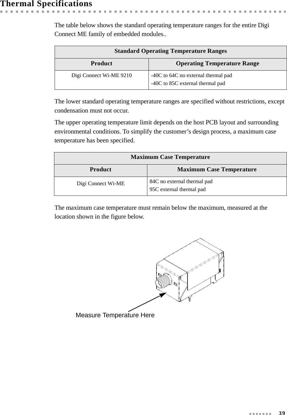
![ 31Note:The CAN Bus interface is available on the 8/16 Digi Connect ME 9210, Wi-ME 9210 variants. Note:When using the 8/16 ME 9210/ Wi-ME 9210 CAN Bus, the DTR (9210 signal GPIO 6) line must be tri-stated. When the DTR signal (9210 GPO/I 6) is used, 9210 GPO/I 15 must be tri-stated. These two 9210 signals are wired together on the 9210 modules.Note:The Digi Connect Wi-ME 9210 module does not provide pins 1-6.Note:When using I2C, make sure to put a 10k pull up on the SDA and SCL lines.Pin[Wi-ME/Wi-ME 9210]Pin[ME/ME 9210]UART[All] GPIO[ME/Wi-ME]GPIO [ME 9210] Ext IRQ[ME/Wi-ME]Ext IRQ[ME 9210/Wi-ME 9210]I2C[ME 9210/Wi-ME 9210]SPI[ME 9210/Wi-ME 9210]FIM[ME 9210/Wi-ME 9210]CAN BUS[ME 9210/Wi-ME 9210]Timer[ME 9210/Wi-ME 9210]Other[All]1VETH+2VETH-3-6 Positions Removed1 7 RXD A3 GPIO[3] DATA IN PIC_0_GEN_IO[3]2 8 TXD A7 GPIO[7] DATA OUT Timer Out 7Timer In 83 9 RTS A5 GPIO[5] 3CLK Timer Out 6410 DTR A6 GPIO[6] PIC_CAN_TXD Timer In 7511 CTS A1 GPIO[1] 0PIC_0_GEN_IO[1]612 DSR A2 GPIO[2] 1PIC_0_GEN_IO[2] PIC_CAN_RXD713 DCD A0 GPIO[0] EN PIC_0_GEN_IO[0]814 /RST915 3.3V10 16 GND11 17 C4 GPIO[12] SDA CLK RESET_DONE12 18 C1 GPIO[9] 1 0 SCL13 19 Reserved14 20 C5 GPIO [13] CLK Timer Out 9 /INIT](https://usermanual.wiki/Digi/50M1745.User-Manual-1/User-Guide-1521485-Page-31.png)
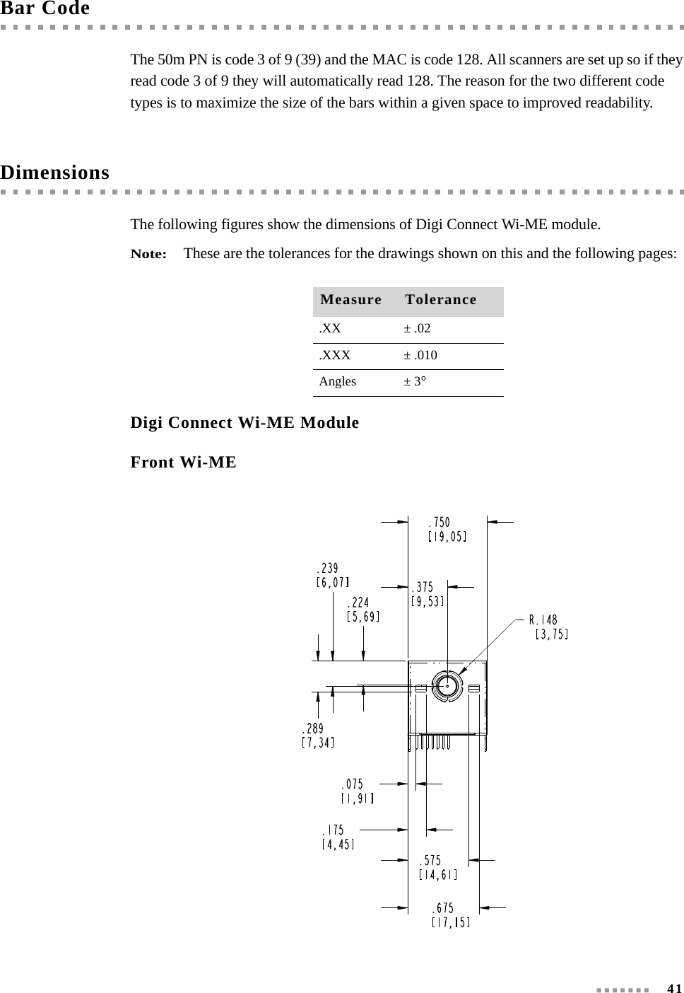
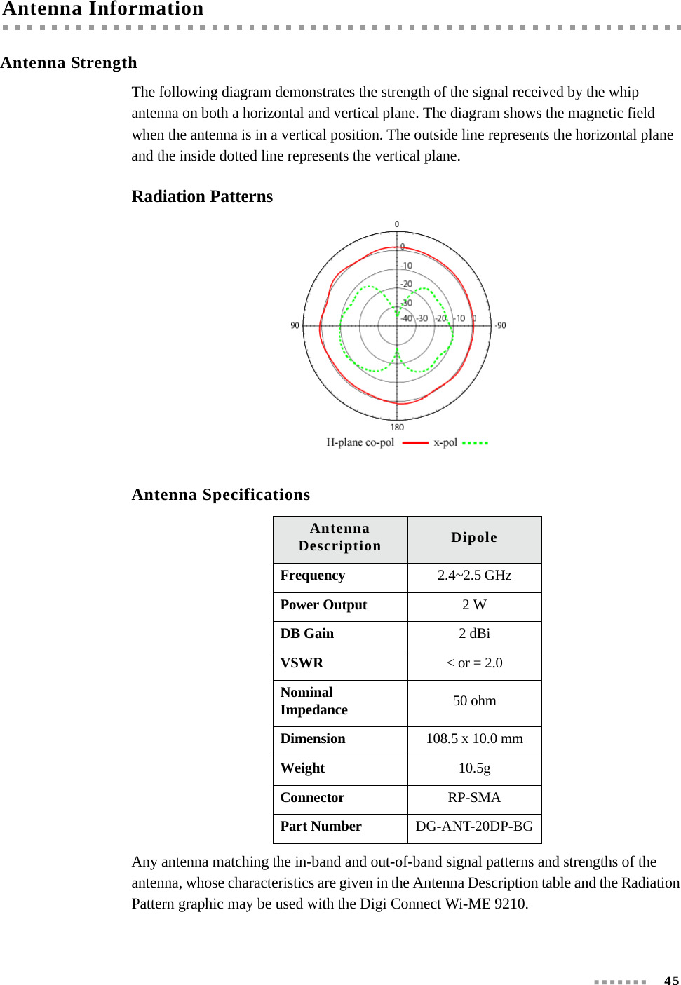
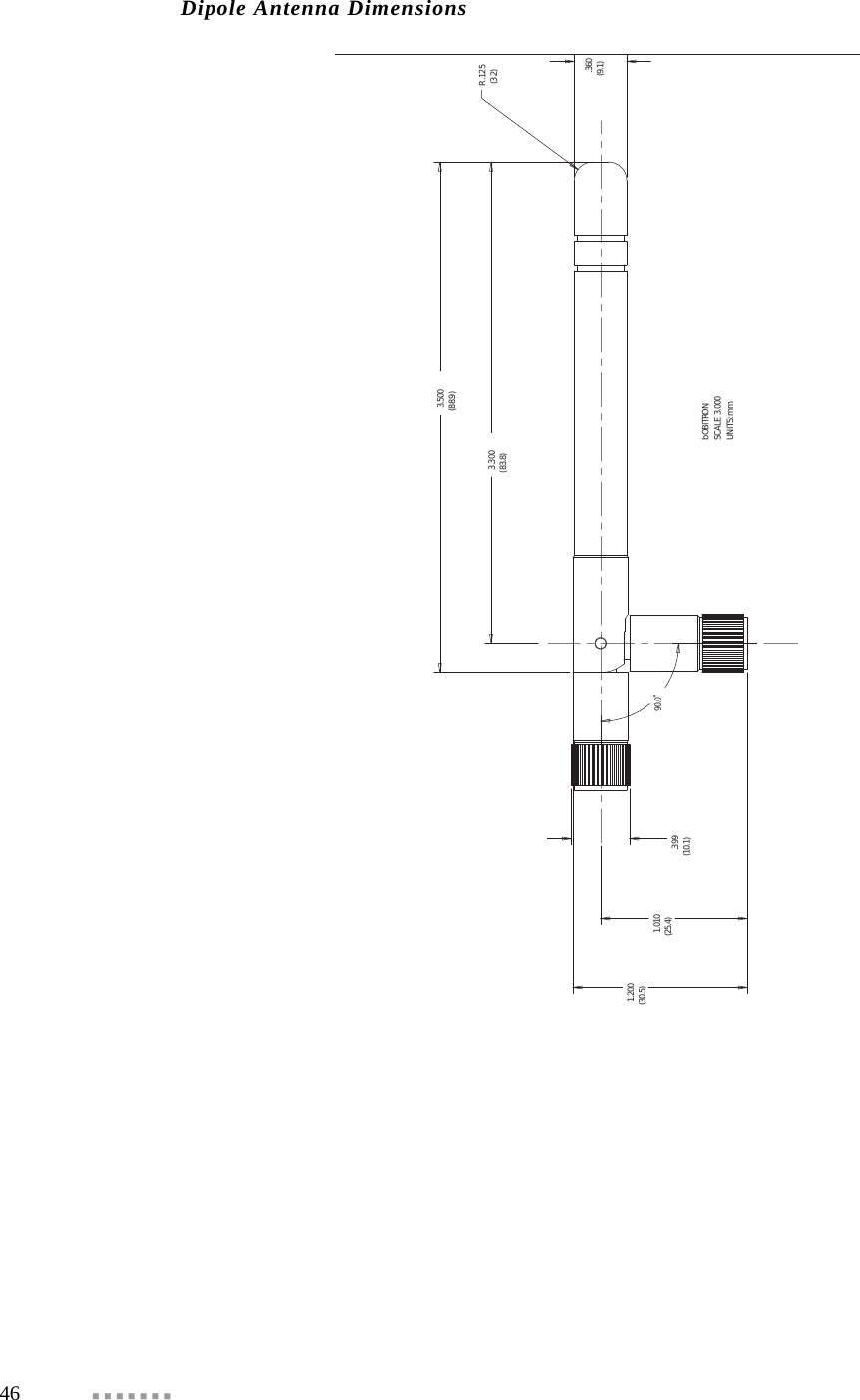

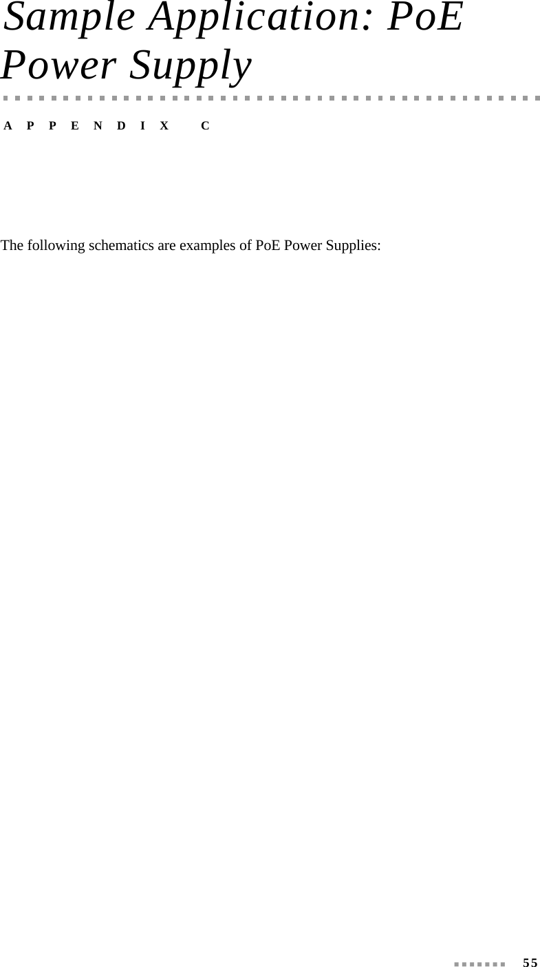
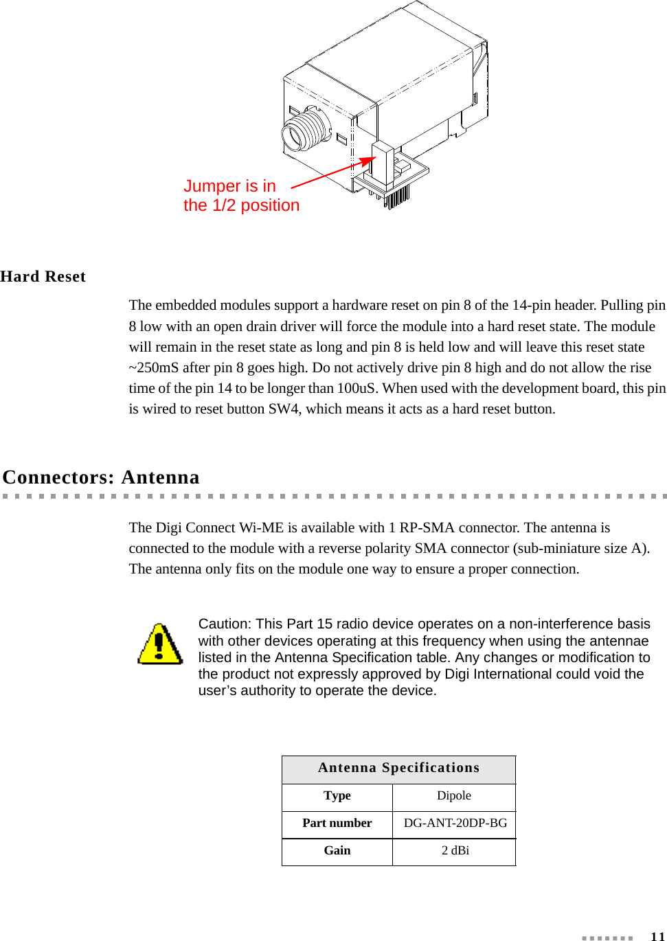
![ 53Antenna configurationsThis device has been designed to operate with the antennas listed below, and having a maximum gain of [10] dBi. Antennas not included in this list or having a gain greater than [10] dBi are strictly prohibited for use with this device. The required antenna impedance is [50] ohms The following antenna configurations that were tested with the Connect Wi-ME 9210 module. Digi 29000095, Bobbintron SA-006-1, +2 dBi dipole antenna (NP-SMA)To reduce potential radio interference to other users, the antenna type and its gain should be so chosen that the equivalent isotropically radiated power (e.i.r.p.) is not more than that permitted for successful communication.](https://usermanual.wiki/Digi/50M1745.User-Manual-1/User-Guide-1521485-Page-53.png)