Digi 50M1745 802.11 b/g/n digital transceiver module User Manual Digi Connect ME and Wi ME Hardware Reference
Digi International Inc 802.11 b/g/n digital transceiver module Digi Connect ME and Wi ME Hardware Reference
Digi >
Contents
- 1. User Manual 1
- 2. User Manual 2
User Manual 1

DigiConnectWi‐ME®9210
HardwareReference
90001247_A
5/3/2011
© 2011 Digi International Inc.
All rights reserved.
Digi, Digi International, the Digi logo, a Digi International Company, Digi Connect, Digi Connect Wi-ME,
ConnectCore, NET+ and NET+OS are trademarks or registered trademarks of Digi International, Inc. in the United
States and other countries worldwide. All other trademarks are the property of their respective owners.
All other trademarks mentioned in this document are the property of their respective owners.
Information in this document is subject to change without notice and does not represent a commitment on the
part of Digi International.
Digi provides this document “as is,” without warranty of any kind, either expressed or implied, including, but
not limited to, the implied warranties of fitness or merchantability for a particular purpose. Digi may make
improvements and/or changes in this manual or in the product(s) and/or the program(s) described in this manual
at any time.
This product could include technical inaccuracies or typographical errors. Changes are periodically made to the
information herein; these changes may be incorporated in new editions of the publication.

3
••••••••••••••••••••••••••••••••••••••••••••••••••••••••
About This Document
Scope of the Reference Manual
The purpose of this document is to enable developers to integrate the Digi Connect Wi-ME
9210 embedded modules with other devices, enabling these devices to make use of the
module’s rich networking features.
Note:
Unless mentioned specifically by name, the products will be referred to as the
embedded modules or modules. Individual naming is used to differentiate
product specific features.
Related Documentation
See the NS9210 Hardware Reference for information on the NS9210 chip.
Support Information
To get help with a question or technical problem or make comments and recommendations
about Digi products and documentation, use the following contact information.
General Customer Service and Support
Digi International
11001 Bren Road East
Minnetonka, MN 55343
U.S.A.
United States: 1 877-912-3444
Other Locations: 1 952-912-3444
www.digi.com/support/eservice/
eservicelogin.jsp
4

5
Contents
About This Document ................................................................................................................3
Related Documentation....................................................................................................3
Support Information ......................................................................................................... 3
Chapter 1: Contents..............................................................................................................5
Chapter 2: About the Digi Connect
Wi-ME Embedded Module7
Overview ..........................................................................................................................7
Types of Modules.............................................................................................................8
Connectors: Power and Device Interface ......................................................................... 9
Connectors: Antenna......................................................................................................11
Module LEDs .................................................................................................................12
Chapter 3: About the Development Board .......................................................................13
Overview ........................................................................................................................13
Basic Description ...........................................................................................................14
Port Descriptions............................................................................................................ 16
Connectors and Blocks................................................................................................... 19
Switches and Push Buttons.............................................................................................24
Development Board LEDs .............................................................................................25
Power Jack P15 ..............................................................................................................27
Test Points......................................................................................................................28
Chapter 4: Programming Considerations.........................................................................29
Overview ........................................................................................................................29
Module Pinout................................................................................................................30
Reset...............................................................................................................................32
Memory ..........................................................................................................................33
Appendix A Module Specifications....................................................................................35
Network Interface...........................................................................................................35
Serial Interface ...............................................................................................................36
Data Rates (bps) .............................................................................................................36
DC Characteristics.......................................................................................................... 36
6
Power Management (Digi Connect ME 9210 only) ...................................................... 38
Thermal Specifications .................................................................................................. 39
Mechanical..................................................................................................................... 40
Bar Code ........................................................................................................................41
Dimensions..................................................................................................................... 41
Recommended PCB Layout........................................................................................... 44
Antenna Information...................................................................................................... 45
RF Exposure Statement.................................................................................................. 47
Safety Statements........................................................................................................... 47
Appendix B Certifications.................................................................................................. 49
FCC Part 15 Class B ...................................................................................................... 49
Industry Canada ............................................................................................................. 50
Declaration of Conformity............................................................................................. 51
International EMC Standards......................................................................................... 52
Appendix C Sample Application: PoE Power Supply ..................................................... 55
Appendix D Sample Application: TTL Signals to EIA-232 ............................................ 59
Appendix E Change Log .................................................................................................... 61

7
About the Digi Connect
Wi-ME Embedded Module
CHAPTER 1
Overview
The Digi Connect Wi-ME 9210 b/g is a fully customizable and secure 802.11b/g wireless
embedded module that provides integration flexibility in a variety of connection options.
Built on the new Digi NS9210 processor in combination with a 802.11bgn Wi-Fi radio, it is
pin-compatible with the existing Digi Connect Wi-ME 802.11b module allowing customers
to easily migrate to the next-generation version of the product.
The NS9210 processor provides a host of features such as an ARM926EJ-S core running at
speeds from 75-150MHz, on-chip AES encryption engine, one PICs, a serial port, SPI and
I2C interfaces, PWM, and others. Most importantly, it is a “drop-in” replacement for the
NS7520, which means that is the ideal upgrade vehicle to deliver a next-generation design.
The integrated FIM on the NS9210 processor offer interface flexibility allowing the
modules to provide high performance interface functionality and unique software-driven
configuration flexibility by dynamically loading software support for application specific
interfaces, e.g. UART, CAN, USB device, 1-Wire, SDIO, and others.
The Digi Connect Wi-ME 9210 embedded module offers freedom and flexibility of
professional embedded software development provided by the easy-to-use, cost-effective
and complete Digi JumpStart Kits™ for NET+OS and Microsoft.NET Micro Framework.
From medical systems to building control and industrial automation, in virtually any
application where embedded device connectivity over a wireless network is needed,
embedded modules are the ideal choice, delivering high-performance functionality.
Note:
Unless mentioned specifically by name, the products will be referred to as the
embedded modules or modules. Individual naming is used to differentiate product
specific features.
This chapter provides information about the modules hardware and contains the following
topics:
"Types of Modules" on page 8
"Connectors: Antenna" on page 11
"JTAG Jumper" on page 10
"Module LEDs" on page 12
8
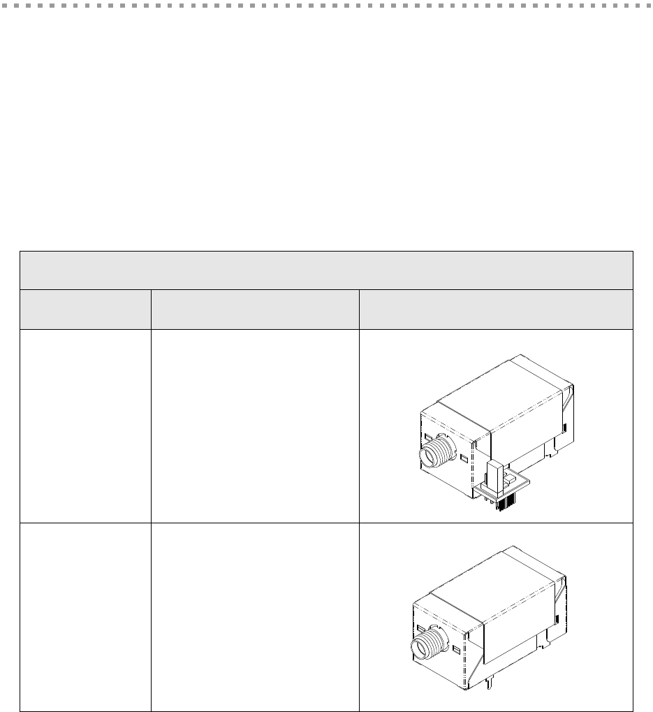
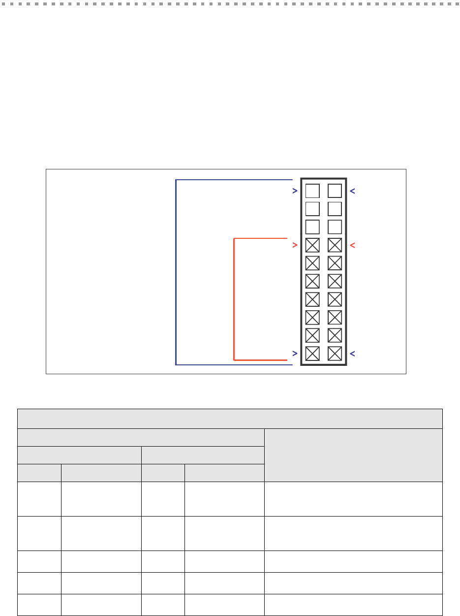
Types of Modules
There are two types of modules. One module utilizes Digi Plug-and-Play Firmware, while
the second is customizable with the option to develop a firmware application in .NET MF
or NET+OS. If you are developing your firmware application in NET+OS, you will be
using a module with a JTAG interface.
Note:
JTAG is a commonly used term that is also referred to as IEEE 1149.1, an industry
standard test protocol. JTAG is an abbreviation for the European Joint Test Action
Group, which invented the first versions of the IEEE 1149.1 interface. The JTAG
interface, along with the other development tools, enables you to download, run
and debug programs on the module.
The following figures show the two types of modules.
Note:
-S: No JTAG for use with Digi Plug-and-Play Firmware
-C: No JTAG for use with custom NET+OS applications
-JT: With JTAG for use with custom firmware development
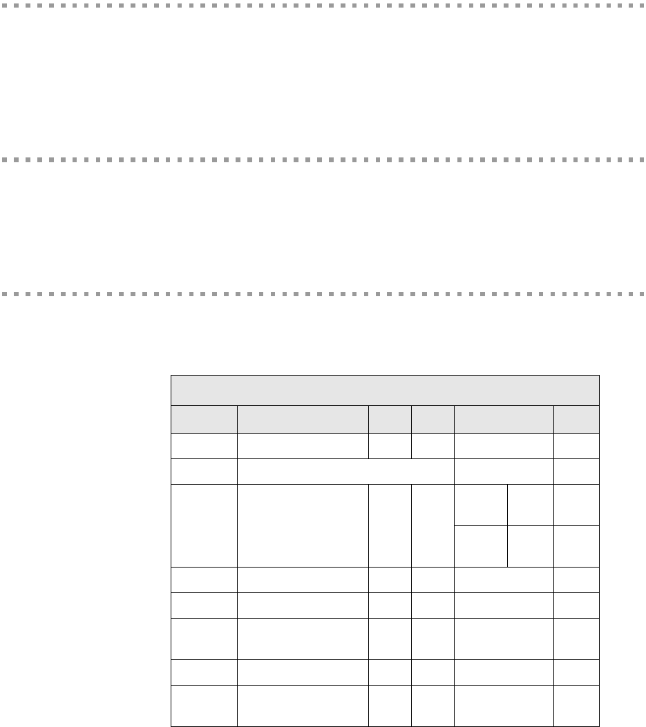
Digi Connect Wi-ME Modules
Model Description Figure
DC-WME-Y402-JT
Used for development
purposes only
JTAG interface
DC-WME-Y402-S
DC-WME-Y402-C
No JTAG interface
Ordered
independently for use
in your
implementation.
9
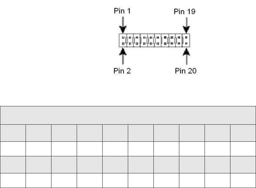
Connectors: Power and Device Interface
Difference in pin assignments/availability
Digi Connect Wi-ME 9210 module uses a 14 pin male connector that fits into the Digi
Connect ME family 20 pin foot print. Pins 1 through 6 are not used and have been removed
from the Connect Wi-ME module. The pin assignment table shows the appropriate values.
Power and Device Interface Connector
Viewed from bottom of the module:
Module Front
ME 20 Pin
Connector
Wi-ME 14 Pin
Connector
Wi-ME Pin 2
ME Pin 1 ME Pin 2
ME Pin 19 ME Pin 20
Wi-ME Pin 1
>
>
>
>
>
>
Bottom View
Power and Device Interface Connector Pin Assignments
Signal
DescriptionME Wi-ME
Pin # Function Pin # Function
1 VETH+ — ME: Power Pass-Thru+
Wi-ME: Position Removed
2 VETH- — ME: Power Pass-Thru-
Wi-ME: Position removed
3-6 — — Position removed
7 RXD 1 RXD Receive Data (Input)
8 TXD 2 TXD Transmit Data (Output)
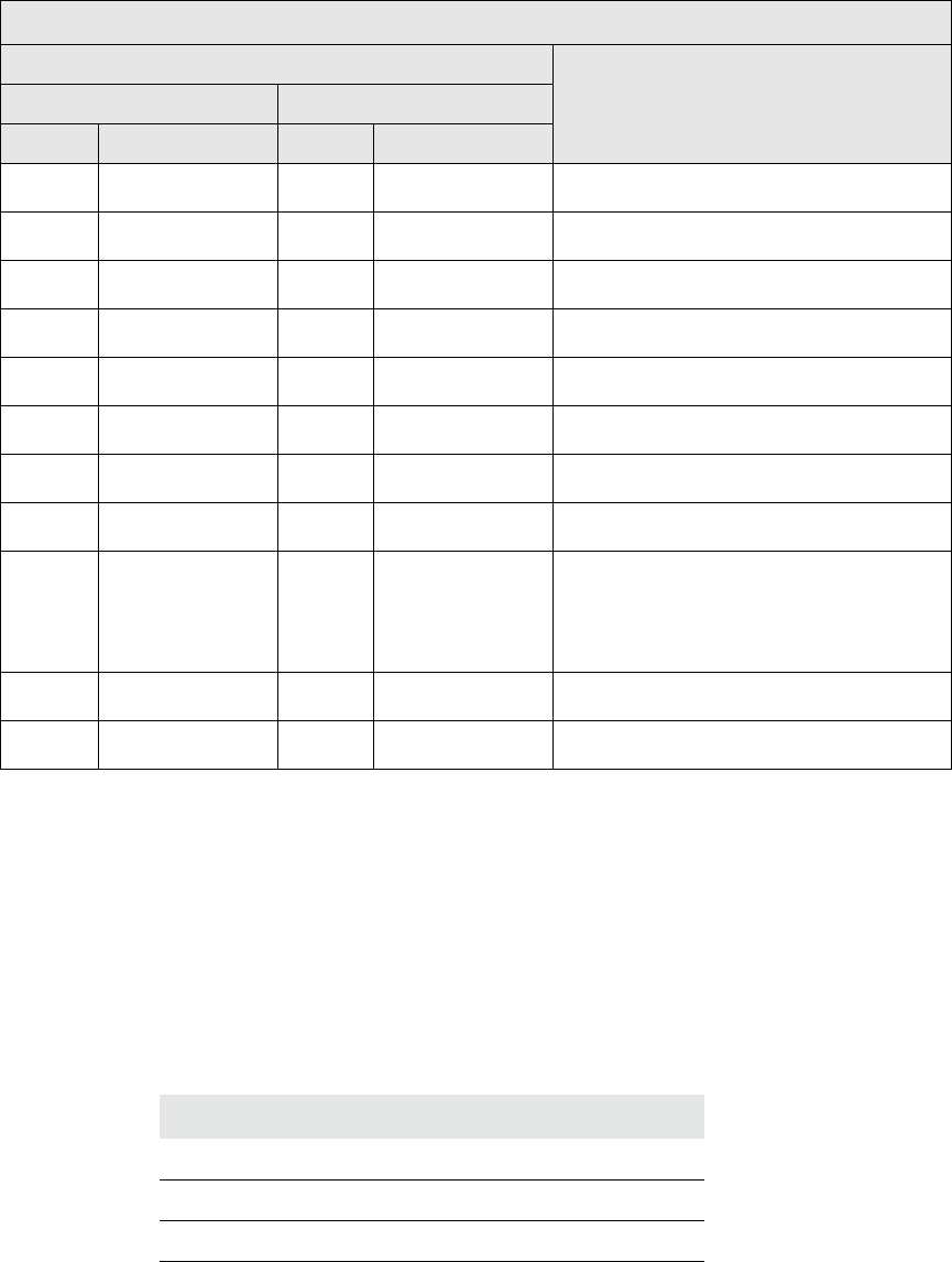
10
Note:
The development board provides connectors for an optional PoE application kit.
Note:
Any pins not used can be left floating.
Note:
See "Module Pinout" on page 30 for detailed IO configuration information.
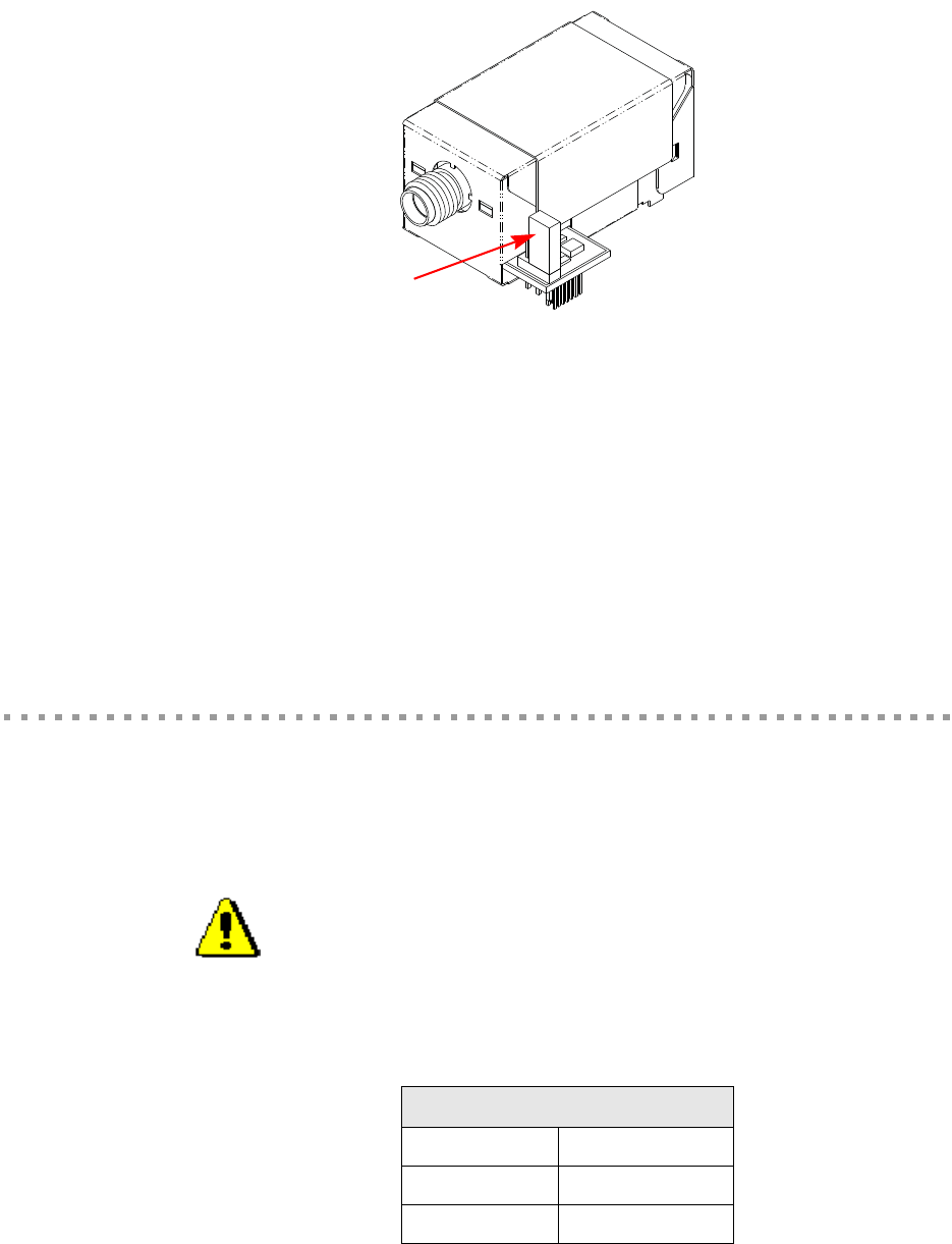
JTAG Jumper
The J1 controls the way in which the Digi Connect Wi-ME 9210 JTAG device responds to
pin 14 being pulled low.
9 RTS 3 RTS Request to Send (Output)
10 DTR 4 DTR
Data Terminal Ready (Output)
11 CTS 5 CTS Clear to Send (Input)
12 DSR 6 DSR Data Set Ready (Input)
13 DCD 7 DCD
Data Carrier Detect (Input)
14 /RESET 8 /RESET Reset
15 +3.3V 9 +3.3V Power
16 GND 10 GND Ground
17, 18 — 11, 12 —
Not accessible with Digi Plug-and-Play
Firmware. If using a development kit, see
"Module Pinout" on page 30 for detailed IO
configuration information.
19 — 13 — Reserved. Do not connect.
20 /INIT 14 /INIT Software Reset
Power and Device Interface Connector Pin Assignments
Signal
DescriptionME Wi-ME
Pin # Function Pin # Function
Jumper Result
None No reset
1-2 Hard reset
2-3 Soft reset
11
Hard Reset
The embedded modules support a hardware reset on pin 8 of the 14-pin header. Pulling pin
8 low with an open drain driver will force the module into a hard reset state. The module
will remain in the reset state as long and pin 8 is held low and will leave this reset state
~250mS after pin 8 goes high. Do not actively drive pin 8 high and do not allow the rise
time of the pin 14 to be longer than 100uS. When used with the development board, this pin
is wired to reset button SW4, which means it acts as a hard reset button.
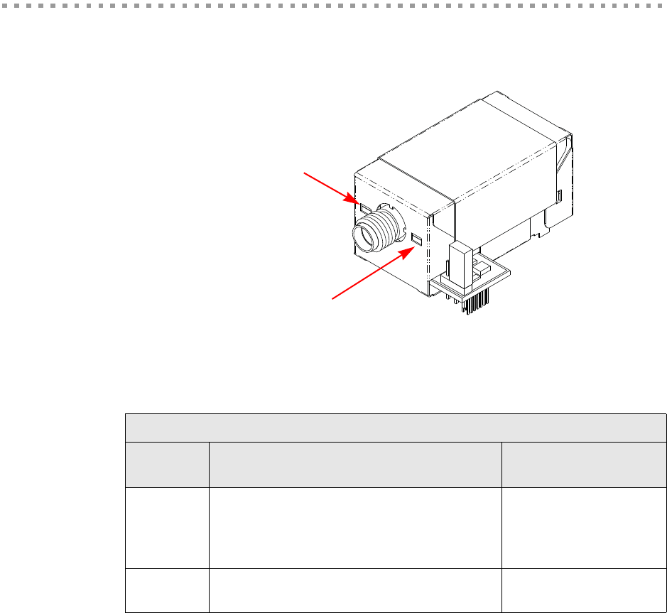
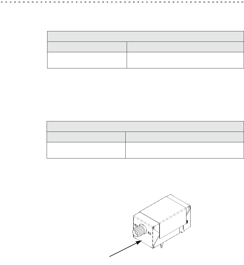
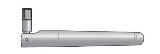
Connectors: Antenna
The Digi Connect Wi-ME is available with 1 RP-SMA connector. The antenna is
connected to the module with a reverse polarity SMA connector (sub-miniature size A).
The antenna only fits on the module one way to ensure a proper connection.
Jumper is in
the 1/2 position
Antenna Specifications
Type Dipole
Part number DG-ANT-20DP-BG
Gain 2 dBi
Caution: This Part 15 radio device operates on a non-interference basis
with other devices operating at this frequency when using the antennae
listed in the Antenna Specification table. Any changes or modification to
user’s authority to operate the device.
the product not expressly approved by Digi International could void the
12
Module LEDs
LED Locations
Note:
The LEDs are the same for a module with or without a JTAG connector.
LED Behaviors
LED Digi Plug and Play Firmware
Digi Connect Wi-ME Customizable Modules
Left
Associated/Diagnostic:
On - unit is associated with an access point.
Blinking slowly - unit is in ad hoc mode.
Blinking quickly - unit is scanning for a network.
Same as Digi Plug-and Play
Firmware (Network link
status).
Right Network Activity:
Blinking -network data is transmitted or received.
This LED is software
programmable.
Network Activity
Associated/Diagnostic

13
About the Development
Board
CHAPTER 2
Overview
The development board is a hardware platform from which you can determine how to
integrate the embedded modules into your design. The board consists of the following main
features:
Socket for connecting the embedded modules
JTAG connection (for use with the development kit only)
GPIO switches
Serial and GPIO ports
Power input
This chapter provides information on development board components and contains the
topics listed below. For more detailed information on the development board, see the
schematic and mechanical drawings on the CD that accompanies your kit. Once you’ve
installed the software that comes with your kit, you can access the schematic from the Start
menu.
"Basic Description" on page 14
"Placement of Module" on page 16
"Connectors and Blocks" on page 19
"Switches and Push Buttons" on page 24
"Development Board LEDs" on page 25
"Power Jack P15" on page 27
"Test Points" on page 28
14
Basic Description
The development board contains connectors, switches, and LEDs for use while integrating
the embedded module into your design. See the following figure for the location of the
connectors, switches, and LEDs. Additionally, the board provides test points (not shown on
the figure). For more information about test points, see "Test Points" on page 28.
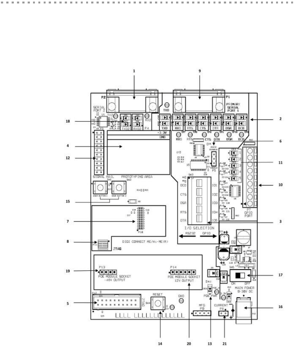
Board Layout and Connector Locations:
15
"Port Descriptions" on page 16
"Connectors and Blocks" on page 19
"Switches and Push Buttons" on page 24
"Development Board LEDs" on page 25
"Power Jack P15" on page 27
See the following figures for placement of either module onto the development board.
Connectors, Switches and LEDs
Board Description Markers 1-5
12345
Secondary
Serial Port, P2
Primary Port
LEDs, CR5 -
CR18
GPIO Switch
Bank, SW3
Prototyping
Area, P4
JTAG
Header, P12
Connectors, Switches and LEDs
Board Description (continued) Markers 6-10
678910
232 Enable
Jumper
Block, P5
Embedded
Module
Connector,
P10
JTAG
Connector,
P11
Primary
Serial Port, P1 GPIO Port, P7
Connectors, Switches and LEDs
Board Description (continued) Markers 11-15
11 12 13 14 15
Digital I/O
LEDs, CR19 -
CR23
Logic
Analyzer
header, P3
POE Source
LED, CR24
Reset Switch,
SW4
User
Pushbuttons,
SW1 & SW2
Connectors, Switches and LEDs
Board Description (continued) Markers 16-21
16 17 18 19 20 21
Power Jack,
P15
On/Off
switch, SW5
Secondary
Port LEDs
CR1-CR4
-48V DC
output from
module P13
12V output
from PoE
module P14
Current
Measurement
Option P8
16
Placement of Module
Port Descriptions
The development board provides the following ports:
Primary Serial Port, P1
Secondary Serial Port, P2
GPIO Port, P7
See the figure titled "Board Layout and Connector Locations:" on page 14 for the location
of the ports. The following sections describe the ports.
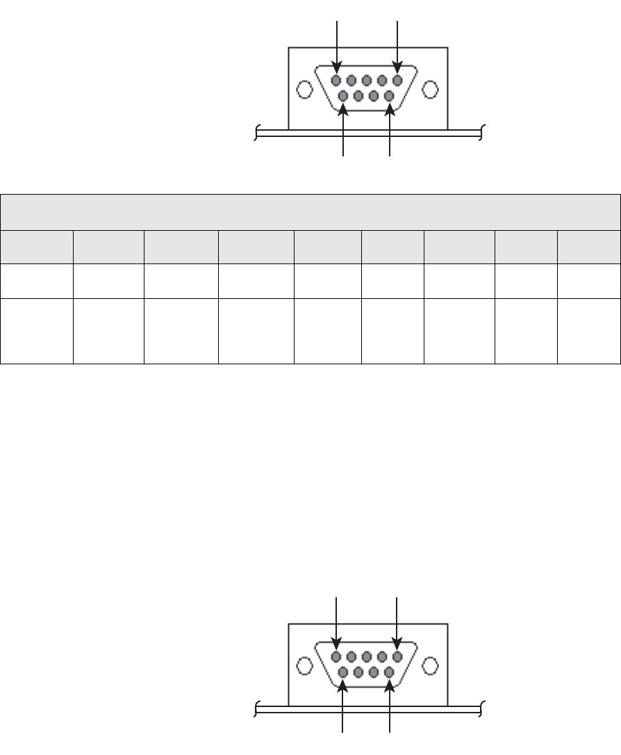
Primary Serial Port, P1
The Primary Serial Port is a DB-9 male connector that is labeled as P1 on the development
board. See the following figure for pin orientation; see the following table for pin
assignments.
Caution: When handling the development board, wear a grounding wrist
strap to avoid ESD damage to the board.
17
Primary Serial Port Pin Orientation
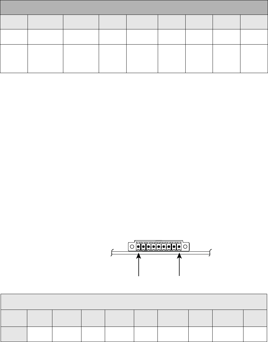
Secondary Serial Port, P2
The Secondary Serial Port is a DB-9 male connector that is labeled as P2 on the
development board. The port is used only with the Digi Connect ME modules with JTAG
interfaces for debugging purposes. See the following figure for pin orientation; see the
following table for pin assignments.
Secondary Serial Port Pin Orientation
Pin 1 Pin 5
Pin 6 Pin 9
Primary Serial Port Pin Assignments
Pin 1 Pin 2 Pin 3 Pin 4 Pin 5 Pin 6 Pin 7 Pin 8 Pin 9
DCD RXD TXD DTR GND DSR RTS CTS —
Data Carrier
Detect
Receive
Data
Transmit
Data
Data
Terminal
Ready
Signal/
Chassis
Ground
Data Set
Ready
Request To
Send
Clear To
Send —
Pin 1 Pin 5
Pin 6 Pin 9
18
RS232-Enable Pin Header, P5
P5 is used to enable or disable serial port RS232s transceiver. Shorting P5 pins 1 and 2 will
enable the RS232 transceiver. Shorting P5 pins 2 and 3 will disable the RS232 transceiver.
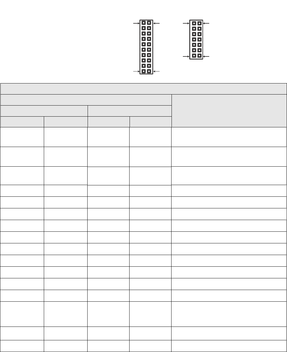
GPIO Port, P7
The GPIO port is a 9-pin male right-angle connector that is labeled as P7 on the
development board. See the following figure for pin orientation; see the following tables
for pin assignments. For input and output threshold specifications, see "DC Characteristics"
on page 36. Note that each signal has a 220 ohm series resistor between the P7 pin and the
module (except GND).
Note:
The development board is shipped with a 9-pin screw-flange plug attached to
the GPIO port.
GPIO Port Pin Orientation
Secondary Serial Port Pin Assignments
Pin 1 Pin 2 Pin 3 Pin 4 Pin 5 Pin 6 Pin 7 Pin 8 Pin 9
—RXD TXD —GND — — — —
—Receive Data Transmit Data —
Signal/
Chassis
Ground
— — — —
Pin 1 Pin 9
GPIO Port Pin Assignments
Pin 1 Pin 2 Pin 3 Pin 4 Pin 5 Pin 6 Pin 7 Pin 8 Pin 9
Signal GPIO-1 GND GPIO-2 GND GPIO-3 TXD_TTL GPIO-4 RXD_TTL GPIO-5

19
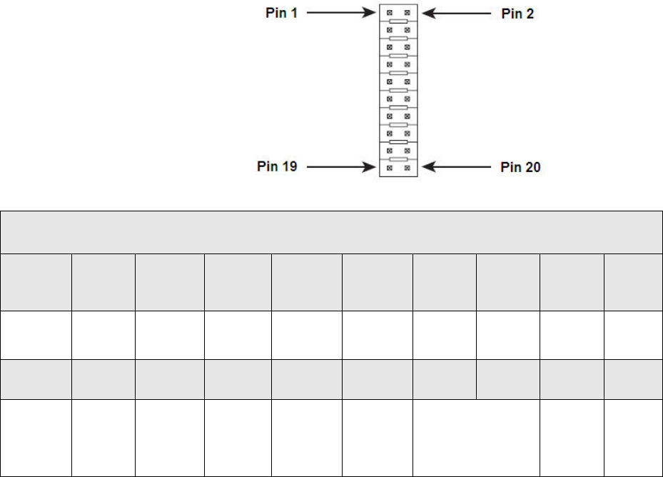
Connectors and Blocks
The development board provides the following connectors and blocks:
Embedded Module Connector, P10
The Digi Connect Wi-ME module does not provide pins 1-6
JTAG Debugger Connector, P12.
-48V DC input to PoE module (Digi Connect ME must be connected to a
Powering Device for this feature.), P13
12V DC output from PoE module into Dev Board Power Supply, P14
Logic Analyzer Header, P3
See the figure titled "Board Layout and Connector Locations:" on page 14 for the location
of the connectors and blocks. The following sections describe the connectors and blocks.
Embedded Module Connector, P10
The Digi Connect ME embedded module Connector is a 20-pin female vertical header that
is labeled P10 on the development board. See the following figure for pin orientation; see
the following table for pin assignments.
Note:
The figure shows the connector using the same orientation as shown in the
figure titled "Board Layout and Connector Locations:" on page 14.
20
Embedded Module Connector Pin Orientation
Note:
The Digi Connect Wi-ME module does not provide pins 1-6
Note:
See "Module Pinout" on page 30 for detailed IO configuration information.
1
19
1
141320
2
2
Connect ME Connect Wi-ME &
Wi-ME 9210
Module Connector Pin Assignments
Signal
DescriptionME Wi-ME
Pin # Function Pin # Function
1VETH+ — — ME: Power Pass-Thru +
Wi-ME: Position removed
2VETH- — — ME: Power Pass-Thru -
Wi-ME: Position removed
3-6 Position
Removed — —
7RXD 1RXD Receive Data (Input)
8TXD 2TXD Transmit Data (Output)
9RTS 3RTS Request to Send (Output)
10 DTR 4DTR Data Terminal Ready (Output)
11 CTS 5CTS Clear to Send (Input)
12 DSR 6DSR Data Set Ready (Input)
13 DCD 7DCD Data Carrier Detect (Input)
14 /RESET 8/RESET Reset
15 +3.3V 9+3.3V Power
16 GND 10 GND Ground
17, 18 —11, 12 —
Not accessible with Digi Plug-and-Play Firmware.
If using a development kit, see "Module Pinout" on
page 30 for detailed IO configuration information.
19 —13 —Reserved
20 /INIT 14 /INIT Digi Plug-and-Play Firmware Software Reset
21
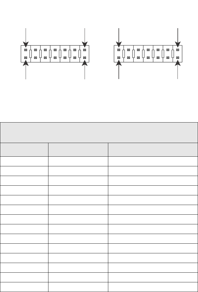
Module JTAG Interface Connector, P11
The Module’s JTAG Interface Connector is a 14-pin female vertical header that is labeled
P11 on the development board. The connector mates with the JTAG connector on the
embedded module. The Module’s JTAG Connector pins are tied to the debugger connector
(see “JTAG Debugger Connector, P12”).
Since the modules' JTAG connectors are mounted on the bottom side of the modules, the
pin 1 location is mirrored from that of the Development board's mating JTAG connector
(P11). The resulting pin mapping is indicated in the Module JTAG Interface Connector Pin
Assignments table below.
Module JTAG Interface Connector
Pin Assignments
JTAG Signal ME JTAG pin # JTAG Connector (P11) pin #
+3.3V 1 2
GND 2 1
TRST# 3 4
GND 4 3
TDI 5 6
GND 6 5
TMS 7 8
GND 8 7
TCK 9 10
RXD 10 9
TDO 11 12
SRST 12 11
+3.3V 13 14
TXD 14 13
Pin 1
Bottom side of module (left) and development board from top (right)
ME JTAG Connector
Development Board
JTAG Connector (P11)
Pin 2
Pin 13
Pin 14
Pin 2
Pin 1
Pin 14
Pin 13
(Bottom View) (Top View)
22
JTAG Debugger Connector, P12
The JTAG debugger connector is a 20-pin male vertical header that is labeled P12 on the
development board. The connector mates with a JTAG debugger plug (for example, a Digi
JTAG Link). The connector is used with the development kit only. See the following figure
for pin orientation. See the following table for pin assignments.
Note:
The figure shows the connector using the same orientation as shown in the
figure titled "Board Layout and Connector Locations:" on page 14.
JTAG Debugger Connector Pin Orientation
JTAG Debugger Connector Pin Assignments
Pin 1 Pin 2 Pin 3 Pin 4 Pin 5 Pin 6 Pin 7 Pin 8 Pin 9 Pin 10
VCC+ VCC+ /TRST GND TDI GND TMS GND TCK GND
Pin 11 Pin 12 Pin 13 Pin 14 Pin 15 Pin 16 Pin 17 Pin 18 Pin 19 Pin 20
RTCK GNO TDO GND /SRST GNO N/A GND N/A GND
23
Logic Analyzer Header, P3
The Logic Analyzer Header is a 20-pin male vertical header that is labeled P3 on the
development board. The header is for connecting a digital signal analyzer (for example, a
logic analyzer) to the development board. See the following figure for pin orientation; see
the following table for pin assignments.
Note:
The figure shows the connector using the same orientation as shown in the
figure titled "Board Layout and Connector Locations:" on page 14.
Logic Analyzer Header Pin Orientation
Logic Analyzer Header Pin Assignments
Pin
1Pin
2Pin 3 Pin 4 Pin 5 Pin 6 Pin 7 Pin 8 Pin
9Pin
10
V_Ether+ V_Ether- Not
Connected
Not
Connected
Not
Connected
Not
Connected RXD TXD GPIO-4 GPIO-5
Pin 11 Pin 12 Pin 13 Pin 14 Pin 15 Pin 16 Pin 17 Pin 18 Pin 19 Pin 20
GPIO-2 GPIO-3 GPIO-1 /RST 3.3v GND
See "Power and Device
Interface Connector Pin
Assignments" on page 9
for details.
Reserved /INIT
24
Switches and Push Buttons
The development board provides the following switches:
User PB1
User PB2
GPIO Switch Bank 1, SW3
Reset, SW4
Power On/Off SW5
See the figure titled "Board Layout and Connector Locations:" on page 14 for the location
of the switches. The following sections describe the switches.
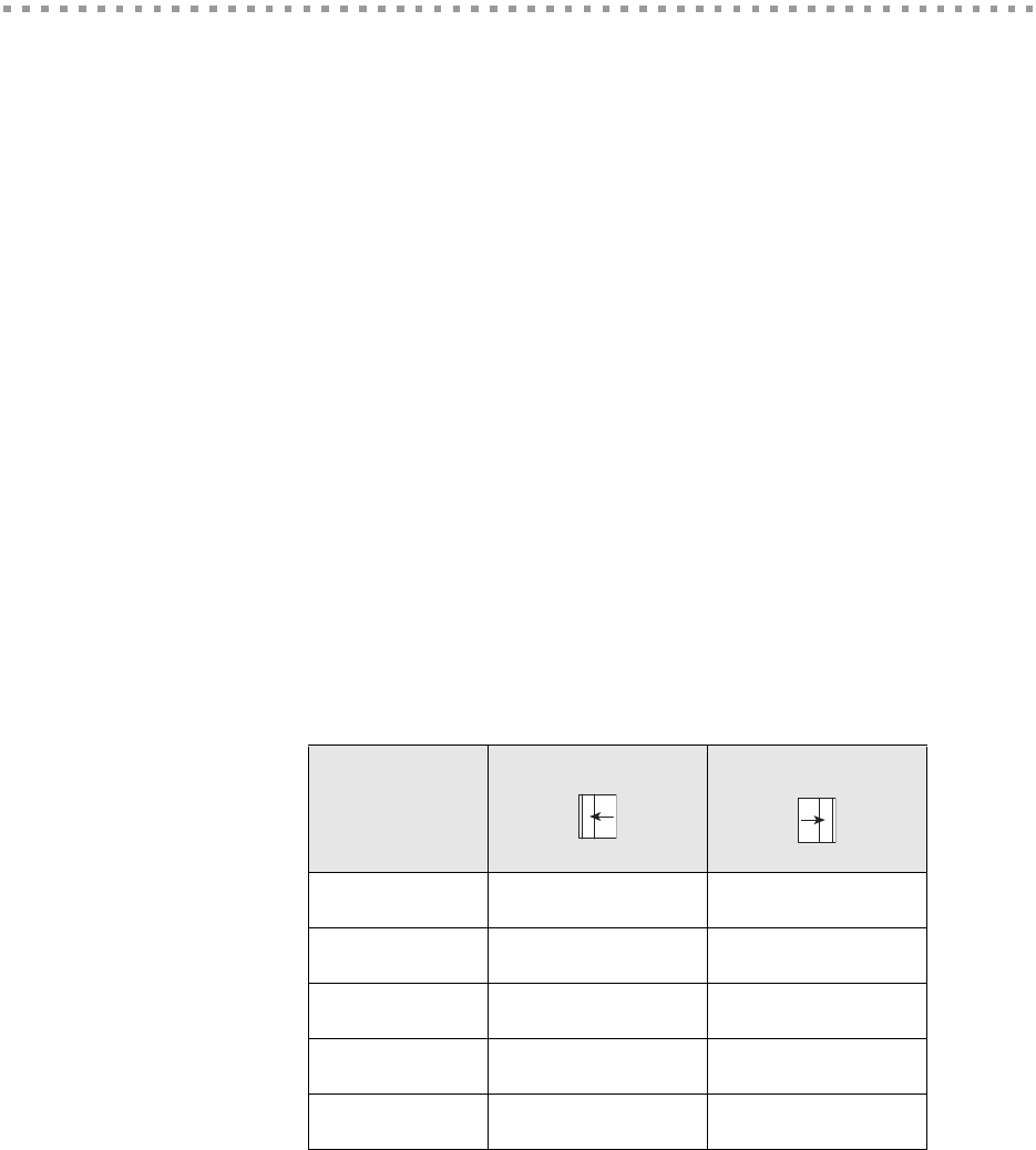
GPIO Switch Bank 1, SW3
GPIO Switch Bank 1, labeled SW3, is a set of five slide switches that allows the embedded
module to use either serial signals or GPIO signals to communicate with a device. With the
switch to the left position, the module’s signal is connected to the Serial Port1 RS232
transceiver. In the right position, the module signal is connected to the appropriate pin of
the GPIO Port P7.
GPIO Switch Bank 1 Settings
User Push Button 1, SW1
When switch number 1 is set to GPIO-1, pushing User Push Button 1, SW1, will drive
GPIO-1 (Wi-ME pin 7, ME pin 12) low.
Switch
Number
Left Position Right Position
1DCD GPIO-1
2CTS GPIO-2
3DSR GPIO-3
4RTS GPIO-4
5DTR GPIO-5
25
User Push Button 2, SW2
Pushing User Push Button 2, SW2, will drive Wi-ME module pin 12 (ME module pin 18)
low.
Reset, SW4
The Reset switch is a push button switch labeled SW4 on the development board. Pressing
the switch holds the embedded module in reset. When the push button is released, the
module reboots.
Power On/Off Switch, SW5
The left position means that power is on. The right position means that power is off.
Development Board LEDs
The development board contains 25 LEDs that are labeled CR1 through CR25. The
following table lists and describes the LEDs.
Development Board LED Descriptions
Board
Label Description
State
Indication
CR1 TXD, Secondary Serial Port Yellow On Logic 1 on TTL, mark, -V on line side
CR2 TXD, Secondary Serial Port Yellow On Logic 1 on TTL, mark, -V on line side
CR3 RXD, Secondary Serial Port Yellow On Logic 1 on TTL, mark, -V on line side
CR4 RXD, Secondary Serial Port Green On Logic 0 on TTL, space, +V on line side
CR5 DCD, Primary Serial Port Yellow On Logic 1 on TTL, mark, -V on line side
CR6 DCD, Primary Serial Port Green On Logic 0 on TTL, space, +V on line side
CR7 DSR, Primary Serial Port Yellow On Logic 1 on TTL, mark, -V on line side
CR8 DSR, Primary Serial Port Green On Logic 0 on TTL, space, +V on line side
CR9 CTS, Primary Serial Port Yellow On Logic 1 on TTL, mark, -V on line side
CR10 CTS, Primary Serial Port Green On Logic 0 on TTL, space, +V on line side

26
CR11 RXD, Primary Serial Port On Logic 1 on TTL, mark, -V on line side
CR12 RXD, Primary Serial Port On Logic 1 on TTL, mark, -V on line side
CR13 DTR, Primary Serial Port Yellow On Logic 1 on TTL, mark, -V on line side
CR14 DTR, Primary Serial Port Green On Logic 0 on TTL, space, +V on line side
CR15 RTS, Primary Serial Port Yellow On Logic 1 on TTL, mark, -V on line side
CR16 RTS, Primary Serial Port Green On Logic 0 on TTL, space, +V on line side
CR17 TXD, Primary Serial Port Yellow On Logic 1 on TTL, mark, -V on line side
CR18 TXD Primary Serial Port Green On Logic 0 on TTL, space, +V on line side
CR19 GPIO 1 Green
On Logic 1
Off Logic 0
CR20 GPIO 2 Green
On Logic 1
Off Logic 0
CR21 GPIO 3 Green
On Logic 1
Off Logic 0
CR22 GPIO 4 Green
On Logic 1
Off Logic 0
CR23 GPIO 5 Green
On Logic 1
Off Logic 0
CR24 POE Active LED Green
On +12v present from POE
Off No POE present
CR25 3.3v LED Green
On Power On
Off Power Off
Development Board LED Descriptions
Board
Label Description
State
Indication
27
Power Jack P15
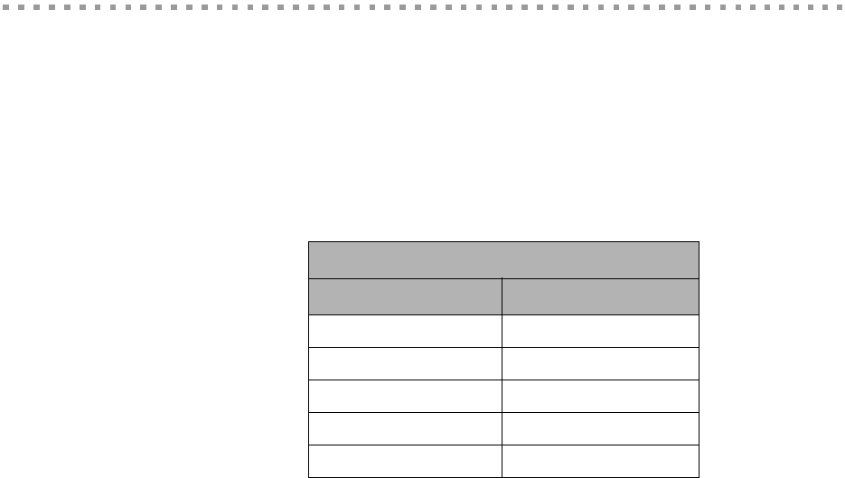
The Power Jack P15 is a barrel connector that accepts 9 to 30 VDC. The following table
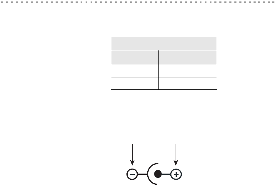
shows the polarity of the power jack.
The following figure schematically represents the polarity of the power jack.
Power Jack Polarity, Schematic
Power Jack Polarity
Contact Polarity
Center +9 to +30 VDC
Outer Ground
Ground +9 to +30 VDC
00000014
28
Test Points
The development board provides 13 test points that can be identified by a board label. The
test point numbers are in the development board schematic drawings. The following table
lists the test point number, board label, and a brief description of each test point.
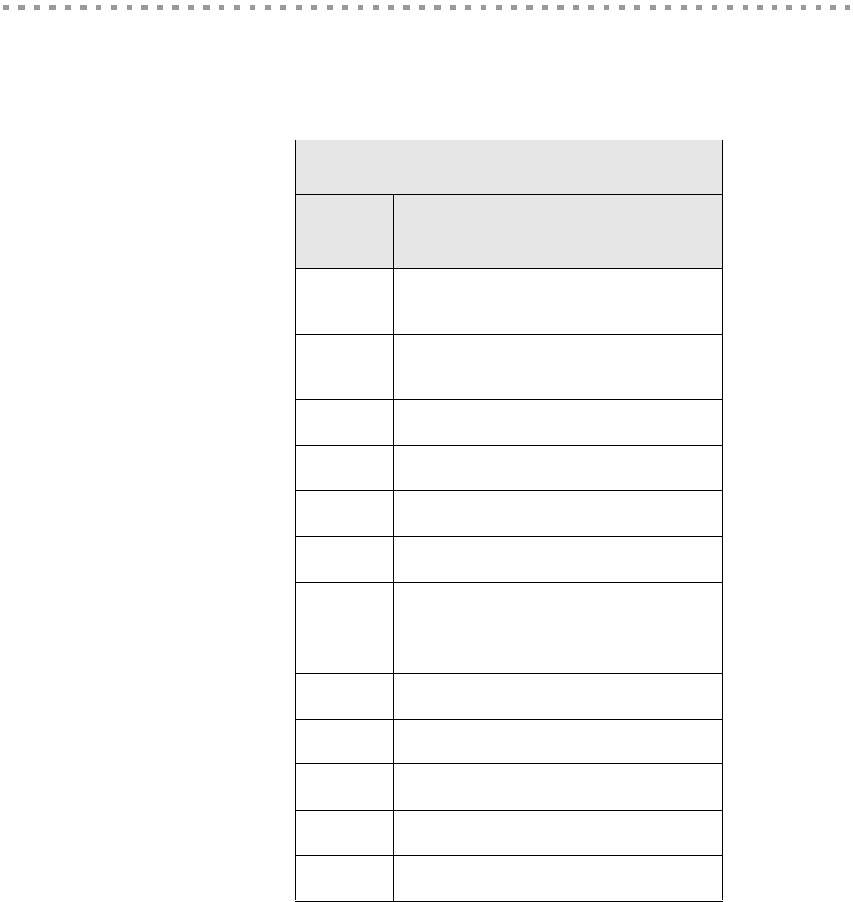
Test Point Descriptions
Test
Point Board Label Description
TP2 TXD TXD-2, Transmit,
Secondary Serial Port
TP3 RXD RXD-2, Receive,
Secondary Serial Port
TP4 CTS CTS, Primary Serial Port
TP5 DTR DTR, Primary Serial Port
TP6 TXD TXD, Primary Serial Port
TP7 RXD RXD, Primary Serial Port
TP8 RTS RTS, Primary Serial Port
TP9 DCD DCD, Primary Serial Port
TP10 DSR DSR, Primary Serial Port
TP12 Reset Reset
TP13 POE 12v POE 12v
TP14 3.3v 3.3v Supply
TP15 GND Ground

29
Programming
Considerations
CHAPTER 3
Overview
This chapter provides information programmers may require to make use of some
embedded module hardware resources. It provides programming information on the
following topics for the Digi Connect ME 9210, the Digi Connect ME and the Digi
Connect Wi-ME:
"Module Pinout" on page 30
"Reset" on page 32
"Memory" on page 33
"SDRAM" on page 33
30
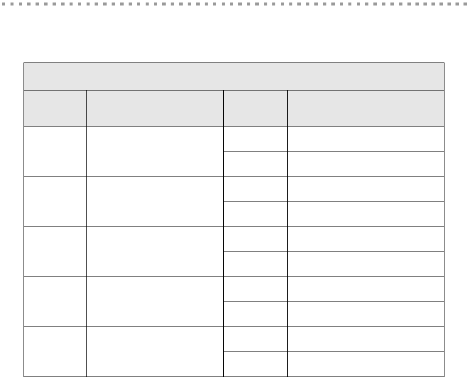
Module Pinout
General Information
The NS7520/NS9210 processors support 16 General Purpose I/O (GPIO) lines, some of
which are reserved for specific functions and some of which can be customized. For Digi
Plug and Play Firmware users, see the Digi Connect Family Users Guide for details on
what Pin configurations are available to you.
Module Pinout
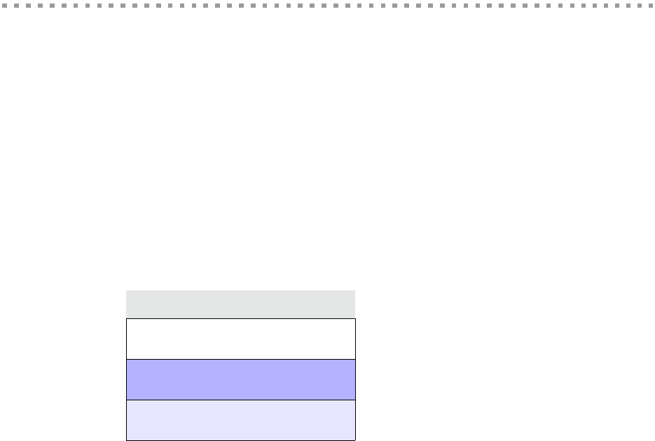
The following table provides signal header pinout information for the Digi Connect ME,
Digi Connect Wi-ME and Digi Connect ME 9210 modules. Please refer to the color key
below.
Key
Applies to Digi Connect ME/Wi-ME
modules.
Applies to Digi Connect ME 9210/Wi-ME
9210 modules.
Applies to Digi Connect ME/Wi-ME and
ME 9210/Wi-ME 9210 modules.

31
Note:
The CAN Bus interface is available on the 8/16 Digi Connect ME 9210, Wi-
ME 9210 variants.
Note:
When using the 8/16 ME 9210/ Wi-ME 9210 CAN Bus, the DTR (9210 signal
GPIO 6) line must be tri-stated. When the DTR signal (9210 GPO/I 6) is used,
9210 GPO/I 15 must be tri-stated. These two 9210 signals are wired together
on the 9210 modules.
Note:
The Digi Connect Wi-ME 9210 module does not provide pins 1-6.
Note:
When using I2C, make sure to put a 10k pull up on the SDA and SCL lines.
Pin
[Wi-ME/
Wi-ME
9210]
Pin
[ME/ME
9210]
UART
[All] GPIO
[ME/
Wi-ME]
GPIO
[ME 9210] Ext
IRQ
[ME/
Wi-ME]
Ext
IRQ
[ME 9210/
Wi-ME
9210]
I2C
[ME 9210/
Wi-ME
9210]
SPI
[ME 9210/
Wi-ME
9210]
FIM
[ME 9210/Wi-
ME 9210]
CAN BUS
[ME 9210/Wi-
ME 9210]
Timer
[ME 9210/
Wi-ME
9210]
Other
[All]
1VETH+
2VETH-
3-6 Positions Removed
1 7 RXD A3 GPIO[3] DATA
IN PIC_0_GEN
_IO[3]
2 8 TXD A7 GPIO[7] DATA
OUT Timer
Out 7
Timer In
8
3 9 RTS A5 GPIO[5] 3CLK Timer
Out 6
410 DTR A6 GPIO[6] PIC_CAN
_TXD Timer In
7
511 CTS A1 GPIO[1] 0PIC_0_GEN
_IO[1]
612 DSR A2 GPIO[2] 1PIC_0_GEN
_IO[2] PIC_CAN
_RXD
713 DCD A0 GPIO[0] EN PIC_0_GEN
_IO[0]
814 /RST
915 3.3V
10 16 GND
11 17 C4 GPIO[12] SDA CLK RESET_
DONE
12 18 C1 GPIO[9] 1 0 SCL
13 19 Reserved
14 20 C5 GPIO [13] CLK Timer
Out 9 /INIT
32
Reset
Hard Reset
The Wi-ME 9210 module supports a hardware reset via pin 8 of the 14-pin header. The unit
is forced into a hard reset when pulling the pin to ground, or less than 0.8v, for one
microsecond. When plugged into a development board, this pin is wired to the push button
at SW4. As a result, this switch acts as a hard reset button.
Reset Characteristics
Characteristic Specification
Delay 250 milliseconds (typical)
Low ActiveThreshold 0.8 V
High Inactive Threshold 2.4V
Minimum Hold Time 1 microsecond pulse
Rise Time 100 microseconds max

33
Memory
Flash
Depending on the variant, the Digi Connect Wi-ME 9210 has 8 or 16MB of flash memory.
The Digi Connect Wi-ME 9210/ARM9 family, the flash memory is controlled by chip
select 2 (default=st_cs1) and is located at 0x50000000.
SDRAM
The Digi Connect Wi-ME 9210’s SDRAM is controlled by chip select 1.
Depending on the variant, the module will have either 8 or 16MB of SDRAM memory.
The following table illustrates typical power consumptions using these power management
mechanisms. These measurements were taken with all Digi NS9210 processor’s I/O clocks
disabled except UART A, UART C, I/O Hub and Memory Clock0 using a standard module
plugged into a Digi JumpStart Kit development board, with nominal voltage applied:
Note 1: The current measurement was taken from the R6 current sense resistor using a 0.025 ohm shunt on the
JumpStart Kit development board. The supply voltage was 3.3V.
Note 2: This is the default power consumption mode when entering applicationStart(), as measured with the
napsave sample application. The value of the NS9210 Clock Configuration register (A090017C) is 0001200B
hexadecimal.
Note 3: This measurement was produced by selecting the “Clock Scale” menu option in the napsave sample
application.
Note 4: This measurement was produced by selecting the “Deep Sleep/Wakeup with an External IRA” menu
option in the napsave sample application.
Mode Power Consumption1
Normal Tx Operational Mode 1.7W (520mA peak)
Normal Receive Operational
Mode21.14W (346mA)
Full Clock Scaling Mode3.613W (186mA)
Sleep Mode4.469/w (146mA)
34

35
Module Specifications
APPENDIX A
Network Interface
Digi Connect Wi-ME 9210
Standard: IEEE 802.11b/g/n
Frequency: 2.4 GHz
Data Rate: Up to 65 Mbps with automatic fallback
Modulation: CCK (11/5 Mbps), DQPSK (2 Mbps),
DBPSK (1 Mbps), OFDM ((6, 9, 12, 18, 24, 36, 48,
54, and 65 Mbps)
Transmit Power: 11 Mbps 17dbm
54/65Mbps 12dbm
Receive sensitivity:
1Mbps: -100
2Mbps: -97
5.5Mbps: -96
6Mbps: -84 dbm
6.5Mbps: -79dbm
9Mbps: -84 dbm
11Mbps: -92
12Mbps: -83 dbm
13Mbps: -76dbm
18Mbps: -81 dbm
19.5Mbps: - 74dbm
24Mbps: -79 dbm
26Mbps: -71dbm
36Mbps: -76 dbm
39Mbps: -67dbm
48Mbps: -72 dbm
52Mbps: -63dbm
54Mbps: -69 dbm
58.5Mbps: -62dbm
65Mbps: -61dbm
Antenna Connector: 1 x RP-SMA
Caution: The Digi Connect Wi-ME 9210 embedded
modules were designed for use in no clean flux wave soldering processes.
The product is not designed to support draining after a water-wash
process, which can lead to water residue inside the enclosure resulting
from direct entry or condensation after the wash process.
36
Serial Interface
One TTL serial interface (CMOS 3.3v) with full modem control signals (DTR, DSR, DCD,
RTS, CTS). The Digi Connect Wi-ME 9210 also supports SPI and FIM-based application
specific interfaces.
Data Rates (bps)
50, 75, 110, 134, 150, 200, 300, 600, 1200, 1800, 2400, 4800, 9600, 14400,19200, 28800,
38400, 57600, 115200, 230400, 460800
DC Characteristics
The following tables provide DC characteristics for operating conditions, inputs, and
outputs.
Warning: The rise time of the 3.3v power supply must be between 700 S and 140ms
and the inrush current must be limited to less than 2 A. A rise time outside of these
limits may cause the device to malfunction and give a 3-1-3 diagnostic error.
Operating Conditions
Symbol Description Min Typ Max Unit
VCC Supply Voltage 3.14 3.3 3.45 V
n/a Power Supply Ripple 40 mVpp
ICC Supply Current — —
Rx
mode 270 mA
Tx
mode
520
(peak)
IIL 16K pull up resistor -10 — 200 A
IIH 16K pull up resistor -10 — 10 A
IOZ HighZ Leakage
Current -10 — 10 A
IOD Output Drive Strength — — 2 mA
CIO Pin Capacitance
(VO=0) — — 4 pF
37
Grounding Recommendation
It is recommended that you connect the tabs on the chassis of the Digi Connect ME / Wi-
ME, and the ground pins directly to the logic ground plane. It is also recommended that you
connect the Digi Connect ME / Wi-ME to the metal chassis of your enclosure. The idea is
to provide the shortest path or a path away from circuitry for ESD to travel to ground.
Inputs
Symbol Description Min Typ Max Unit
VIH Input High Voltage 2 — VCC+0.3a
a.) All I/O are 5v tolerant.
V
VIL Input Low Voltage VSS-0.3 — .8 V
Outputs
Symbol Description Min Typ Max Unit
VOH Output High Voltage Vdd -.6V —Vdda
a.) All I/O are 5v tolerant.
V
VOL Output Low Voltage 0 — 0.4 V
IOH Output High Current 2 — — mA
IOL Output Low Current 2 — — mA
Digi Connect ME Digi Connect Wi-ME
Storage
Temperature
-40°F to 257°F
(-40°C to 125°C)
Relative Humidity Not to exceed 95% non-condensing (4° C to 45°C), constant
absolute humidity above 45°C
Altitude 12000 feet
(3657.60 meters)

38
Power Management (Digi Connect ME 9210 only)
Using the Digi NET+OS development environment, applications on the Digi Connect Wi-
ME 9210 are capable of operating the module in several reduced power consumption
modes. These reduced power operating modes utilize the power management mechanisms
for the NS9210 processor for CPU clock scaling and sleep.
In the Clock Scaling mode, the system itself continues to execute instructions, but at a
different clock rate, which can be changed on-the-fly, using Digi’s patented circuitry inside
the NS9210 processor. The clock speed is changed programmatically to lower or raise the
system clock speed, thus reducing or increasing the module’s power footprint, respectively.
Additionally, a Sleep mode is available in which the system stops executing instructions.
Based on the application needs, wake-up triggers can be set up programmatically to
activate the processor back to wherever it left off. In this mode, a drastic power reduction is
realized by reducing the power consumption of the NS9210 processor and the on-module
PHY.
For sample power consumption figures for normal (typical) and power management related
operation of the Digi Connect Wi-ME 9210, see below:
3.3VDC @ 346 mA typical (1.14W)
UART and Rx activated
Sleep Mode (approximate)
3.3VDC @ 142mA
39
Thermal Specifications
The table below shows the standard operating temperature ranges for the entire Digi
Connect ME family of embedded modules..
The lower standard operating temperature ranges are specified without restrictions, except
condensation must not occur.
The upper operating temperature limit depends on the host PCB layout and surrounding
environmental conditions. To simplify the customer’s design process, a maximum case
temperature has been specified.
The maximum case temperature must remain below the maximum, measured at the
location shown in the figure below.
Standard Operating Temperature Ranges
Product Operating Temperature Range
Digi Connect Wi-ME 9210 -40C to 64C no external thermal pad
-40C to 85C external thermal pad
Maximum Case Temperature
Product Maximum Case Temperature
Digi Connect Wi-ME 84C no external thermal pad
95C external thermal pad
Measure Temperature Here
40
Additional Design Recommendations
The following list provides additional design guidance with respect to thermal management
in applications with operating temperatures at the high end or beyond the specified standard
ambient temperature range.
Providing air movement will improve heat dissipation.
The host PCB plays a large part in dissipating the heat generated by the module.
A large copper plane located under the Digi Connect Wi-ME 9210 and soldered
to the module’s mounting tabs will improve the heat dissipation capabilities of
the PCB.
If the design allows, added buried PCB planes will also improve heat
dissipation. The copper planes create a larger surface to spread the heat into the
surrounding environment.
Adding a thermal pad or thermal compound, such as Sil-Pad®, Gap Pad® or
Gap Filler products made by the Bergquest Company
(www.bergquistcompany.com), between the host PCB and the underside of the
module will significantly increase the thermal transfer between the module’s
enclosure and the host PCB. Limit the fill area to the folded metal portion of the
module’s underside.
Mechanical
Dimensions Digi Connect
Wi-ME
Length 1.445 in.
(36.703 mm)
Width 0.75 in. (19.05 mm)
Height 0.854 in. (21.69 mm)
Weight .616oz.
17.463g
Device/serial
interface connector
14-pin micro header (7-pin
double row) with .05-inch
(1.27-mm) pitch.
41
Bar Code
The 50m PN is code 3 of 9 (39) and the MAC is code 128. All scanners are set up so if they
read code 3 of 9 they will automatically read 128. The reason for the two different code
types is to maximize the size of the bars within a given space to improved readability.
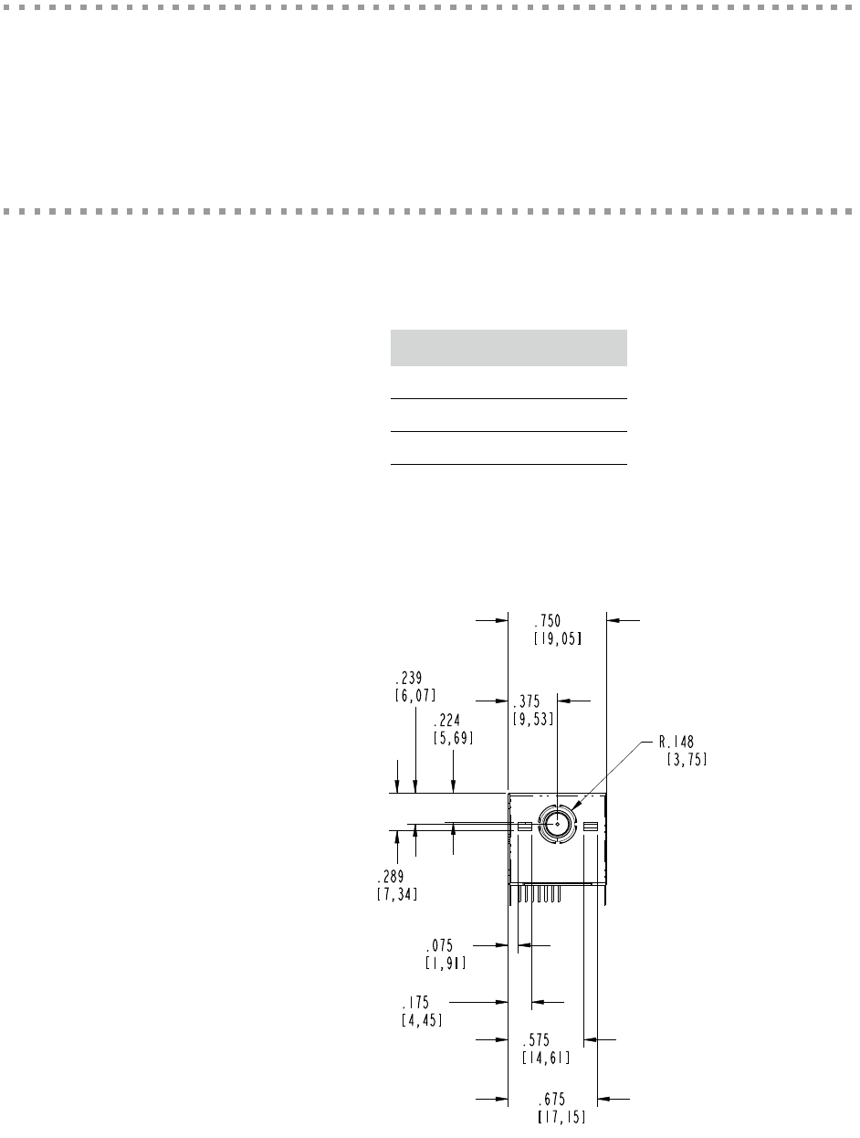
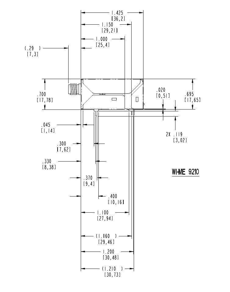
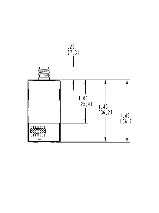
Dimensions
The following figures show the dimensions of Digi Connect Wi-ME module.
Note:
These are the tolerances for the drawings shown on this and the following pages:
Digi Connect Wi-ME Module
Front Wi-ME
Measure Tolerance
.XX ± .02
.XXX ± .010
Angles ± 3°
42
Side Wi-ME
43
Bottom Wi-ME
44
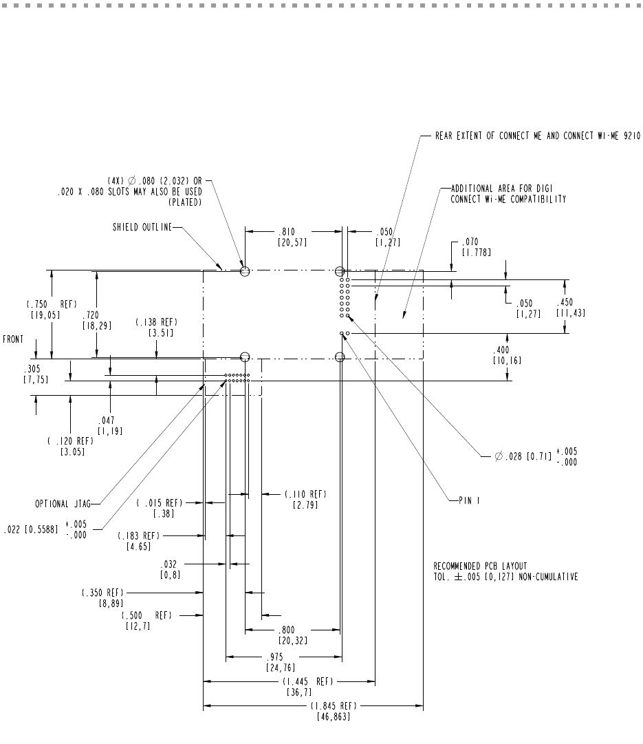
Recommended PCB Layout
The following figure shows the recommended PCB (printed circuit board) layout of the
Digi Connect Wi-ME.
Digi Connect ME and Wi-ME
45
Antenna Information
Antenna Strength
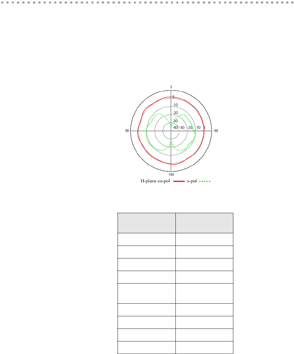
The following diagram demonstrates the strength of the signal received by the whip
antenna on both a horizontal and vertical plane. The diagram shows the magnetic field
when the antenna is in a vertical position. The outside line represents the horizontal plane
and the inside dotted line represents the vertical plane.
Radiation Patterns
Antenna Specifications
Any antenna matching the in-band and out-of-band signal patterns and strengths of the
antenna, whose characteristics are given in the Antenna Description table and the Radiation
Pattern graphic may be used with the Digi Connect Wi-ME 9210.
Antenna
Description Dipole
Frequency 2.4~2.5 GHz
Power Output 2 W
DB Gain 2 dBi
VSWR < or = 2.0
Nominal
Impedance 50 ohm
Dimension 108.5 x 10.0 mm
Weight 10.5g
Connector RP-SMA
Part Number DG-ANT-20DP-BG
46
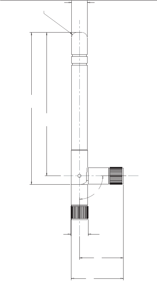
Dipole Antenna Dimensions
bOBITRON
SCALE 3.000
UNITS: mm
90.0˚
(9.1)
.360
(88.9)
3.500
(30.5)
1.200
(25.4)
1.010
(83.8)
3.300
(10.1)
.399
R
(3.2)
.125

47
RF Exposure Statement
The Digi Connect Wi-ME 9210module complies with the RF exposure limits for humans
as called out in RSS-102. It is exempt from RF evaluation based on its operating frequency
of 2.4 GHz, and effective radiated power less than the 3 watt requirement for a mobile
device (>20 cm separation) operating at 2.4 GHz.
Safety Statements
To avoid contact with electrical current:
Never install electrical wiring during an electrical storm.
Never install an ethernet connection in wet locations unless that connector is
specifically designed for wet locations.
Use caution when installing or modifying ethernet lines.
Use a screwdriver and other tools with insulated handles.
You and those around you should wear safety glasses or goggles.
Do not place ethernet wiring or connections in any conduit, outlet or junction
box containing electrical wiring.
Installation of inside wire may bring you close to electrical wire, conduit,
terminals and other electrical facilities. Extreme caution must be used to avoid
electrical shock from such facilities. You must avoid contact with all such
facilities.
Ethernet wiring must be at least 6 feet from bare power wiring or lightning rods
and associated wires, and at least 6 inches from other wire (antenna wires,
doorbell wires, wires from transformers to neon signs), steam or hot water
pipes, and heating ducts.
Do not place an ethernet connection where it would allow a person to use an
ethernet device while in a bathtub, shower, swimming pool, or similar
hazardous location.
Protectors and grounding wire placed by the service provider must not be
connected to, removed, or modified by the customer.
Do not touch un-insulated ethernet wiring if lightning is likely!
Do not touch or move the antenna(s) while the unit is transmitting or receiving.
Do not hold any component containing a radio such that the antenna is very
close to or touching any exposed parts of the body, especially the face or eyes,
while transmitting.
Do not operate a portable transmitter near unshielded blasting caps or in an
explosive environment unless it is a type especially qualified for such use
Any external communications wiring you may install needs to be constructed to all
relevant electrical codes. In the United States this is the National Electrical Code Article
800. Contact a licensed electrician for details.
48

49
Certifications
APPENDIX B
These products comply with the following standards.
FCC Part 15 Class B
Radio Frequency Interference (RFI)(FCC 15.105)
The Digi Connect ME and Digi Connect Wi-ME embedded modules have been tested and
found to comply with the limits for Class B digital devices pursuant to Part 15 Subpart B,
of the FCC Rules. These limits are designed to provide reasonable protection against
harmful interference in a residential environment. This equipment generates, uses, and can
radiate radio frequency energy, and if not installed and used in accordance with the
instruction manual, may cause harmful interference to radio communications. However,
there is no guarantee that interference will not occur in a particular installation. If this
equipment does cause harmful interference to radio or television reception, which can be
determined by turning the equipment off and on, the user is encouraged to try and correct
the interference by one or more of the following measures:
Reorient or relocate the receiving antenna.
Increase the separation between the equipment and the receiver.
Connect the equipment into an outlet on a circuit different from that to which
the receiver is connected.
Consult the dealer or an experienced radio/TV technician for help.

50
Labeling Requirements (FCC 15.19)
This device complies with Part 15 of FCC rules. Operation is subject to the following two
conditions: (1) this device may not cause harmful interference, and (2) this device must
accept any interference received, including interference that may cause undesired
operation.
If the FCC ID is not visible when installed inside another device, then the outside of the
device into which the module is installed must also display a label referring to the enclosed
module FCC ID. This exterior label can use wording such as the following: “Contains
Transmitter Module FCC ID: MCQ-50M1745 / IC: 1846A-50M1745
Modifications (FCC 15.21)
Changes or modifications to this equipment not expressly approved by Digi may void the
user's authority to operate this equipment.
Industry Canada
This digital apparatus does not exceed the Class B limits for radio noise emissions from
digital apparatus set out in the Radio Interference Regulations of the Canadian Department
of Communications.
Le present appareil numerique n'emet pas de bruits radioelectriques depassant les limites
applicables aux appareils numeriques de la class B prescrites dans le Reglement sur le
brouillage radioelectrique edicte par le ministere des Communications du Canada.

51
Declaration of Conformity
Digi Connect Wi-ME 9210Conformity
(In accordance with FCC Dockets 96-208 and 95-19)
Digi International declares, that the product:
to which this declaration relates, meets the requirements specified by the Federal
Communications Commission as detailed in the following specifications:
Part 15, Subpart B, for Class B Equipment
FCC Docket 96-208 as it applies to Class B personal
Computers and Peripherals
The product listed above has been tested at an External Test Laboratory certified per FCC
rules and has been found to meet the FCC, Part 15, Class B, Emission Limits.
Documentation is on file and available from the Digi International Homologation
Department.
Manufacturer's Name: Digi International
Corporate Headquarters: 11001 Bren Road East
Minnetonka MN 55343
Manufacturing Headquarters: 10000 West 76th Street
Eden Prairie MN 55344
Product Name: Digi Connect Wi-ME 9210 embedded module
Model Number: 50001745
52
International EMC Standards
The Digi Connect ME and Digi Connect Wi-ME embedded modules meet the following
standards:
Digi Connect ME Digi Connect Wi-ME
Storage
Temperature
-40°F to 257°F
(-40°C to 125°C)
Relative Humidity Not to exceed 95% non-condensing (4° C to 45°C), constant
absolute humidity above 45°C
Altitude 12000 feet
(3657.60 meters)
Standards Digi Connect
ME Digi Connect
Wi-ME
Emissions
AS/NZS 3548
AS/NZS 3548 CISPR 22
Japan IOH
003NY04115 0000
003GZ04064 0000
FCC Part 15 Subpart C
(FCC ID: MCQ-50M880)
IC RSS 210 (IC:1846A-50M880)
FCC Part 15 Subpart B
ICES-003
EN 55022
EN 61000-4-2
EN 61000-4-3
EN 61000-4-6
EN 301 489-3
EN 300 328
VCCI
Immunity EN 55024
Safety
UL 60950-1
CSA 22.2 No. 60950--1
EN 60950
53
Antenna configurations
This device has been designed to operate with the antennas listed below, and having a
maximum gain of [10] dBi. Antennas not included in this list or having a gain greater than
[10] dBi are strictly prohibited for use with this device. The required antenna impedance is
[50] ohms
The following antenna configurations that were tested with the Connect Wi-ME 9210
module.
Digi 29000095, Bobbintron SA-006-1, +2 dBi dipole antenna (NP-SMA)
To reduce potential radio interference to other users, the antenna type and its gain should be
so chosen that the equivalent isotropically radiated power (e.i.r.p.) is not more than that
permitted for successful communication.
54

55
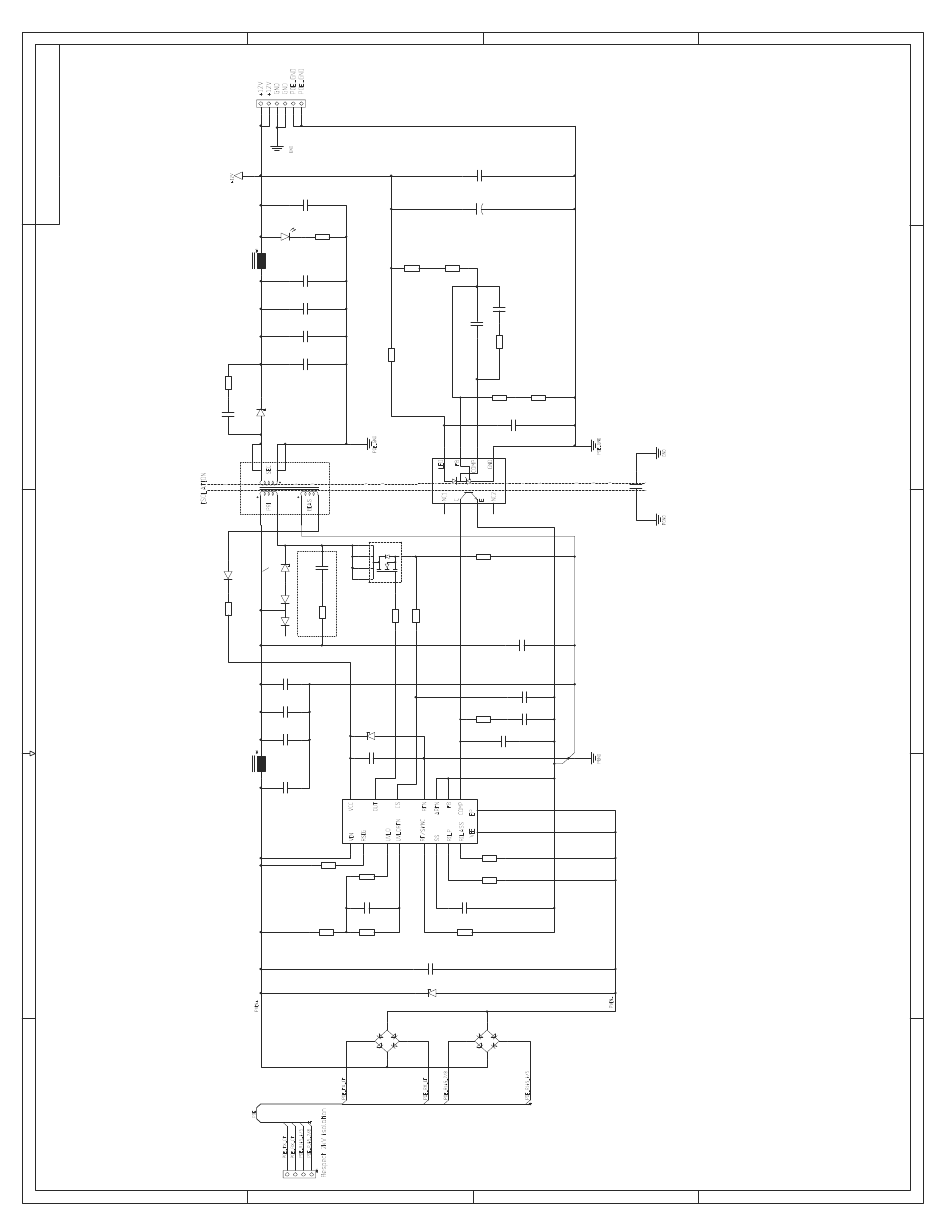
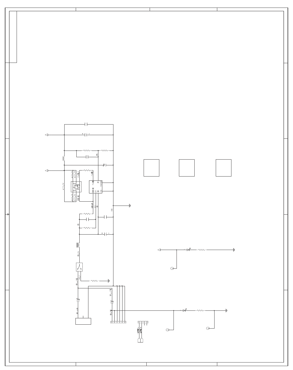
Sample Application: PoE
Power Supply
APPENDIX C
The following schematics are examples of PoE Power Supplies:
56
2/8 Digi Connect ME
5
5
B
A
1234
1234
C
D
D
C
B
A
MB2S
D1
3
4
2
1
ACAC
POS NEG
MB2S
D2
3
4
2
1
ACAC
POS NEG
LM5070SD
U1
12
13
11
9
3
6
2
14
15
4
5
1
7
10
17
8
16
SMAJ60A-13-F
D3
100n/100V
C2
24K9
R1
1K
R2
220n/100V
C3
33K2
R3
590K
R4
15K
R5
47n/100V
C4
100K
R6
53R6
R7
1K
R8
47n/100V
C5
FOD2741ASDV
4
18
5
7
36
2
U2
47R
R9
100R
R10
1u/10V
C7
18R
R11 LL4148
D4
1n/50V
C6
0R33
R12
3.3u
C9
1n/50V
C10
47n/100V
C11
1u/10V
C12
100n/100V
C15
100n/100V
C16
33R
R17
100n/100V
C20
RED
CR1
10u/10V
C27
10u/10V
C28
10u/10V
C29
1K
R21
1K
R16
10K
R14
0R
R24
56V
D11
D12
3
21
100n/100V
C30
1n/100V
C32
1K
R27
1u/10V
C33
D14
1u/10V
C34
2u2/100V
C36
2u2/100V
C37
2u2/100V
C38
3K3
R28
1K8
R29
4K7
R30
220P/50V
C39
330u/35V
C40
+
4p_R/A_TSM
4
3
2
1
P1
6p_R/A_TSM
6
5
4
3
2
1
P2
4,7uH
L5
4,7uH
L6 SS26
D15
FDC2512
56
21
4
3
U3
T1
C1586-ALD
1
2
3
74
8
9
10
NOT POP
Dual 100V
NC
NC
NC
12V/200mW
60V/2A
57
4/8 Digi Connect ME modules and Digi Connect ME 9210 modules
A
B
C
DD
C
1234
4321
A
B
5
5
TP14
1
TEST POINT
+3. 3V
CR25
3.3V LE D
R13
2
1
220
GND
VR1
26
8
71
4
5
LM3485
R10
2
1
15k
R9
2
1
100mohms
R7
2
1
45.3k
U7
1
2
6
5
3
4
FDC5614P
R8
1
2
47
L1
1
2
21000122
22uH
C31
1
2
270pF
GND
+3. 3 V
R11
2
1
24.9k
+3. 3V _ S W
L2
1
2
D8
2
1
C28
1
2
100uF
C23
100uF
2
1
C26
1uF
1
2
C29
0.1uF
1
2
C30
2
1
1uF
P13
4
3
2
1
18000335
P14
6
5
4
3
2
1
18000336
D9
21
TP15
TEST POINT
1
TP13
TEST POINT
1
CR24
3.3V LE D
R12
220
1
2
GND
P15
3
2
1
JACK 3P LOCKING
18000302
2
1
D10
R19
2
1
100mohms
GND
3000XXX1-XX
SCHEMATIC
1
30006001-04 R evA
PCB1
3000XXX2-XX
PCB
1
30006002-04 R evA
PCB2
AS E E MBLY S HT 1 & 2
3000XXX 4-XX
AS S E MBLY
1
30006004-04 R evA
12
3
SW5
SW_SLIDE_SPDT
Vout = 3.29V
Vripp = 26.5mV
58

59
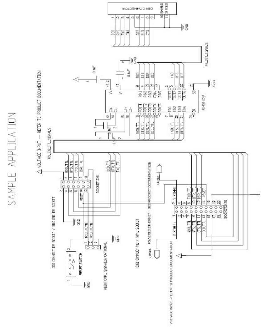
Sample Application:
TTL Signals to EIA-232
APPENDIX D
The following schematic is an example of how to convert the modules’s TTL signals to
EIA-232.
60

61
Change Log
APPENDIX E
The following changes have been made since the last revision of this document.
62