Digi 50M1782 ConnectCore Wi-i.MX53 User Manual 90001270 C 2
Digi International Inc ConnectCore Wi-i.MX53 90001270 C 2
UserManual.wiki
>
Digi
>
50M1782 User Manual
>
Manual pt. 1
Contents
1.
Manual pt. 1
2.
Manual pt. 2
3.
Manual part 1
4.
manual part 2
Manual pt. 1
Navigation menu
Upload a User Manual
Namespaces
Wiki Guide
HTML
PDF
Info
Views
User Manual
Discussion / Help
Navigation
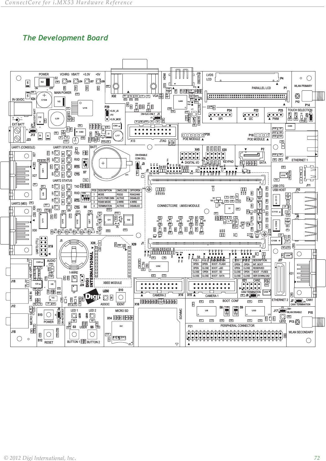
![ȱ ȱ ȱ ȱ ȱ ȱȱ ȱ ȱ ȱ ȱȱȱȱȱMemoryOverviewThe i.MX53 processor has an External Memory Controller (EXTMC) that services all the external memory access requests. The EXTMC provides the arbitration interface and different external memory controllers in order to support several memory devices:M4IF – Multi Master Multi Memory InterfaceESDRAMC – Enhanced DDR memory controllerNFC – NAND flash memory controllerEIM – SRAM/PSRAM/NOR/NOR flash memory controllerDDR2 SDRAM Memory The ConnectCore for i.MX53 module provides up to 2GB of DDR2-800 SDRAM memory. On the module in the development kits four 16-bit, 128Mbit, DDR2-800 chips, configured as two banks of 32-bits of 128Mbits DDR2-800 memory are used.NAND Flash MemoryThe ConnectCore for i.MX53 module provides 8GB of NAND flash memory. On the module in the development kits a 512MByte, 2Kbyte page, NAND flash chip is used. This NAND flash device is connected to NAND flash Chip Select 0.The NAND flash controller signals are available on the module connectors.External Interface Module (EIM)The External Interface Module (EIM) is used on the ConnectCore for i.MX53 module to control the Ethernet Controller. This device is connected to EIM Chip Select 1.The EIM signals are available on the module connectors.System BootThe ConnectCore for i.MX53 boot process begins at Power On Reset when the hardware reset logic forces the ARM core to begin execution starting from the on-chip boot ROM. Boot ROM code uses the state of the internal register BOOT_MODE[1:0] as well as the state of various eFUSEs and/or GPIO settings to determine the boot flow behavior of the module.The ConnectCore for i.MX53 supports the following boot modes:Internal boot– The module boots from the internal ROM– Program Image loaded from the chosen boot device– Boot flow controlled by GPIO and eFUSE (GPIO overrides eFUSE settings)– Supports a secure boot using HAB](https://usermanual.wiki/Digi/50M1782.Manual-pt-1/User-Guide-1709931-Page-36.png)
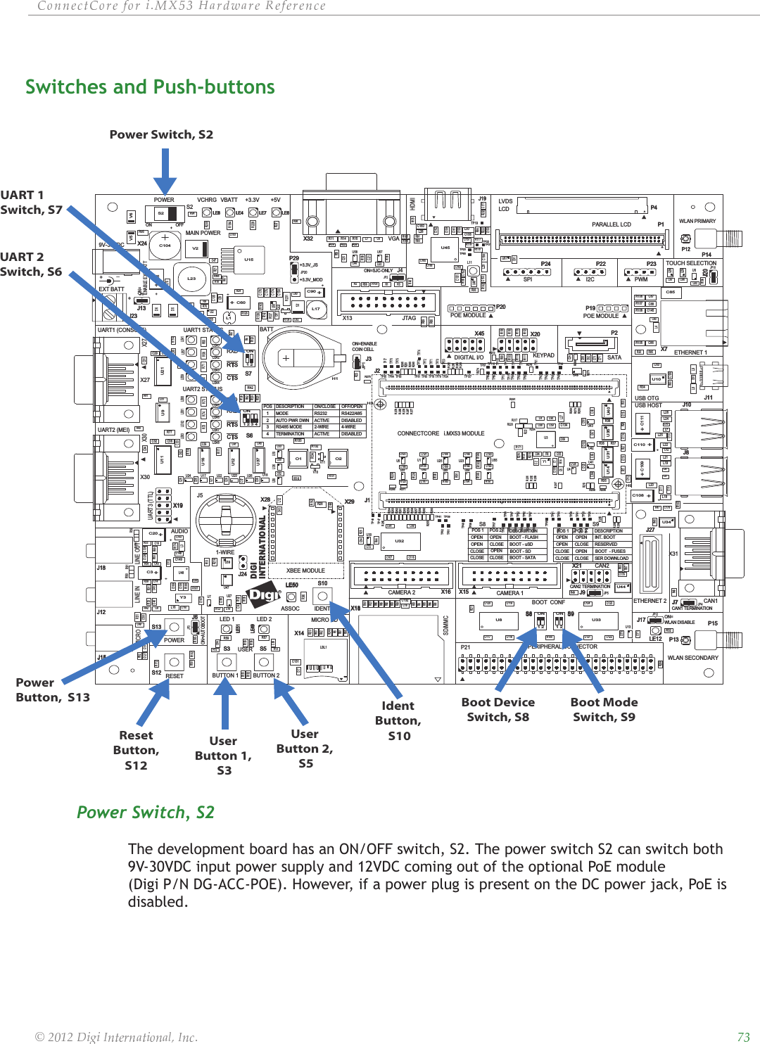
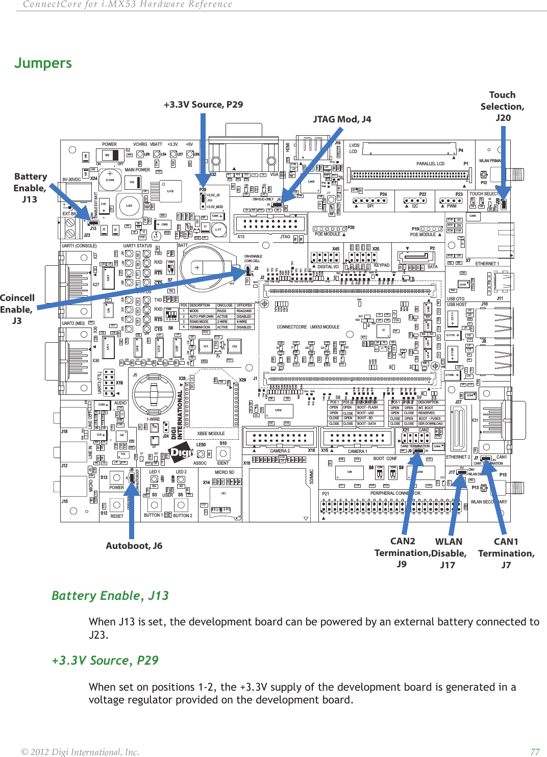
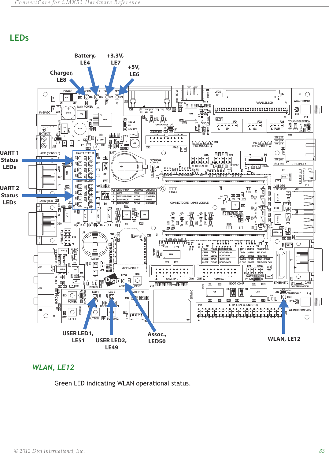
![ȱ ȱ ȱ ȱ ȱ ȱȱ ȱ ȱ ȱ ȱȱȱReset Button, S12The reset push-button S12, resets the module and the peripherals on the development board. A push-button allows manual reset by connecting POR# or optionally RSTIN# to ground.Power Button, S13The power button S12 generates a power event for the i.MX53 and the DA9053 PMIC.When the module is in Off mode, a Power event will power on the module. When the module is in On mode, a long press (>2sec) of the power button will turn off the module. When the module is in On mode, a short press of the power button will put the module in suspend mode (low power). When the module is in Suspend mode, a short press of the power button will resume the module.User Buttons, S3 and S5Use the user push-buttons to interact with the applications running on the ConnectCore for i.MX53 module. Use these module signals to implement the push-buttons:Ident Button, S10The Ident push-button S10 is associated to the commissioning input of the Digi XBee modules. This input provides a variety of simple functions to aid in deploying devices in a network. For a deeply description of this functionality please refer to the Digi XBee modules documentation.Legend for Multi-Position SwitchesSwitches S6, S7, S8 and S9 are multi-pin switches. In the description tables for these switches, the position is designated as S[switch number].[pin number]. For example, position 1 on switch S6 is specified as S6.1.](https://usermanual.wiki/Digi/50M1782.Manual-pt-1/User-Guide-1709931-Page-74.png)