Digi 50M1782 ConnectCore Wi-i.MX53 User Manual 90001270 C 2
Digi International Inc ConnectCore Wi-i.MX53 90001270 C 2
Digi >
Contents
- 1. Manual pt. 1
- 2. Manual pt. 2
- 3. Manual part 1
- 4. manual part 2
Manual pt. 1

ConnectCoreTM
for i.MX53TM
Hardware Reference
90001270_C
5/29/2012

ȱ ȱ ȱ ȱ ȱȱȱȱȱ
©2012 Digi International Inc.
All rights reserved.
Digi, Digi International, the Digi logo, a Digi International Company, Digi JumpStart Kit, ConnectCore, and XBee
are trademarks or registered trademarks of Digi International, Inc. in the United States and other countries
worldwide. All other trademarks are the property of their respective owners.
All other trademarks mentioned in this document are the property of their respective owners.
Information in this document is subject to change without notice and does not represent a commitment on the
part of Digi International.
Digi provides this document “as is,” without warranty of any kind, either expressed or implied, including, but
not limited to, the implied warranties of fitness or merchantability for a particular purpose. Digi may make
improvements and/or changes in this manual or in the product(s) and/or the program(s) described in this manual
at any time.
This product could include technical inaccuracies or typographical errors. Changes are periodically made to the
information herein; these changes may be incorporated in new editions of the publication.

ȱ ȱ ȱ ȱ ȱȱȱ
Contents
Chapter 1: About the Module ........................................................12
Features and Functionality 13
Module Variant 14
Block Diagram 15
CPU 15
Module 16
Module Pinout 17
Pinout Legend 17
Pinout Definitions 17
J1 Pinout 17
J2 Pinout 25
Power 32
Module Power Supplies 32
Supply Inputs 32
Battery input (VLIO) 32
Charger input (VCHRG) 33
Coin Cell input (VCC_COINCELL) 33
Supply Outputs 34
+3.3V 34
+2.775V 34
+1.8V 34
+3.15V 34
DA9053 Power Management 35
Memory 36
Overview 36
DDR2 SDRAM Memory 36
NAND Flash Memory 36
External Interface Module (EIM) 36
ȱ ȱ ȱ ȱ ȱȱȱ
ȱ ȱ ȱ ȱ ȱ ȱ
System Boot 36
Audio Subsystem 37
Video Subsystem 37
Multiplexed GPIO 39
GPIO Multiplexing Table 39
Interfaces 46
1-Wire 46
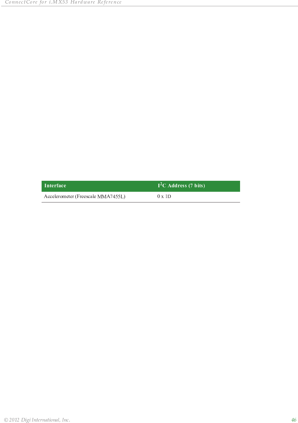
Accelerometer 46
ADC and Touch Screen 47
CAN 47
Clock Amplifier (CAMP) 48
Configurable SPI (CSPI) 49
Digital Audio MUX (AUDMUX) 49
Enhanced Configurable SPI (ECSPI) 49
Ethernet 1 50
Ethernet 2 50
External Interface Module (EIM) 51
General Purpose Input/Output (GPIO) 51
Graphics Processing Unit 2D (GPU2D) 52
Graphics Processing Unit 3D (GPU3D) 54
I2C 54
Image Processing Unit (IPU) 55
Keypad 57
LVDS Display Bridge (LDB) 57
Memory Cards (MMCI/eMMC/SD/SDIO) 58
PWM 59
ConnectCore for i.MX53 PWM 59
DA9053 PWM 59
RTC 60
Known Issue with the RTC 60
SATA 61
ȱ ȱ ȱ ȱ ȱȱȱ
ȱ ȱ ȱ ȱ ȱ ȱ
SPDIF 61
Synchronous Serial Interface (SSI) 62
Television Encoder (TVE) 63
UART 63
USB Host and USB OTG 64
Video Processing Unit (VPU) 66
Watchdog Timer 66
WLAN 67
WLAN 67
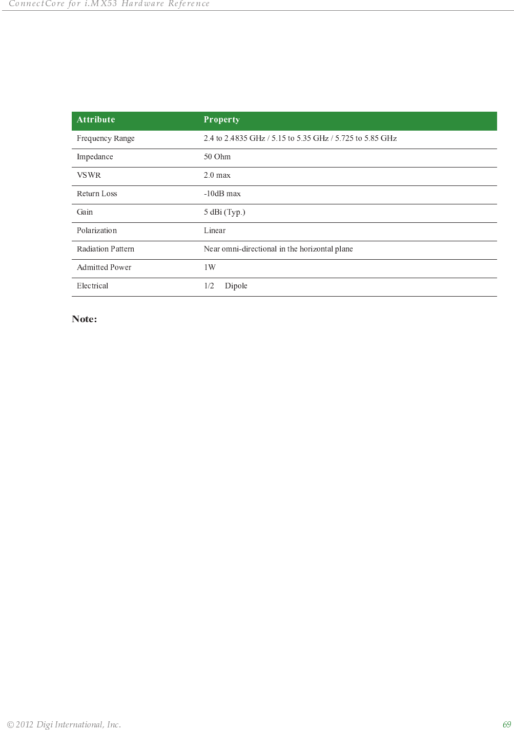
Cable Specification: U.FL/W.FL to RP-SMA 68
Attributes 68
Dimensions 68
Antenna Specification: RP-SMA 69
Attributes 69
SAR Requirements 69
Labelling Requirements 69
Chapter 2: About the Development Board ........................................70
What’s on the Development Board? 70
The Development Board 72
Switches and Push-buttons 73
Power Switch, S2 73
Reset Button, S12 74
Power Button, S13 74
User Buttons, S3 and S5 74
Ident Button, S10 74
Legend for Multi-Position Switches 74
UART 1 Switch, S7 75
UART 2 Switch, S6 75
Boot Device Switch, S8 76
Boot Mode Switch, S9 76
ȱ ȱ ȱ ȱ ȱȱȱ
ȱ ȱ ȱ ȱ ȱ ȱ
Jumpers 77
Battery Enable, J13 77
+3.3V Source, P29 77
WLAN Disable, J17 78
Touch Selection, J20 78
Coincell Enable, J3 78
JTAG Mod, J4 78
Autoboot, J6 78
CAN1 Termination resistor, J7 78
CAN2 Termination resistor, J9 78
Configuration Resistors 79
CSI0_RESET#/KEY_ROW7, R203/R204 80
CSI1_RESET#/KEY_COL7, R201/R202 80
CSI1_HSYNC#/DISP1_HSYNC, R256/R292 80
CSI1_VSYNC#/DISP1_VSYNC, R255/R293 81
UART1_CTS/SD3_CMD, R283/R284 81
UART1_RTS/SD3_CLK, R281/R282 81
DIGIO0/XBEE_RESET#, R277/R287 82
DIGIO1/XBEE_SLEEP_RQ, R278/R288 82
DIGIO2/XBEE_ON_SLEEP#, R280/R289 82
LEDs 83
WLAN, LE12 83
Power LEDs LE4, LE6, LE7 and LE8 84
User LEDs, LE49 and LE51 84
Serial Status LEDs 84
UART 1 Status LEDs 85
UART 2 Status LEDs 85
XBee Assoc., LE50 85
Analog Video Interface (VGA) 86
Analog Video Connector, X32 86
ȱ ȱ ȱ ȱ ȱȱȱ
ȱ ȱ ȱ ȱ ȱ ȱ
Audio Interface 88
Line-out Connector Pinout, J18 89
Line-in Connector Pinout, J12 89
Microphone Connector Pinou, J15 89
Camera Interfaces 90
X15 Pinout 91
X16 Pinout 92
CAN Interface 93
CAN 1, X31 94
CAN 2, X21 94
Charger Power Connector 95
Coin Cell Battery 96
Digital IO Interface 97
Digital I/O Connector, X45 98
Ethernet 1 Interface 99
Ethernet 1, RJ-45 Connector X7 100
Ethernet 2 Interface 101
Ethernet 2, Connector J17 102
HDMI Interface 103
HDMI Connector, J19 104
I2C Interface 105
I2C Header, P22 106
JTAG Interface 107
Standard JTAG ARM Connector, X13 108
LVDS LCD Interface 109
MicroSD™ Card Interface 111
MicroSD™ Connector, X14 112
Module Connectors, J1 and J2 113
Parallel LCD Interface 114
ȱ ȱ ȱ ȱ ȱȱȱ
ȱ ȱ ȱ ȱ ȱ ȱ
Peripheral Application Header 117
Peripheral Application Header, P21 118
Power-Over-Ethernet (PoE) - IEEE802.3af 120
The PoE Module 121
PoE Connector (power in), P19 121
PoE Connector (power out), P20 122
PWM Interface 123
Power Header, P23 124
SATA Interface 125
SATA Connector, P2 126
SD Card Interface 127
SD/MMC Connector, X18 128
SPI Interface 129
SPI Header, P24 130
UART Interface 131
UART 1 (Console), X27 131
UART 2 (MEI), X30 132
UART 3 (TTL Interface), X19 133
USB Host Interface 134
USB Host Connectors, J8 and J10 134
USB OTG Interface 135
USB OTG Connector, J11 135
User Interface 136
WLAN Interface 137
Antenna Connectors (WLAN) 138
Digi XBee Interface 139
Digi XBee Module Connectors, X28 and X29 140
Appendix A: Module Specifications ............................................... 141
ȱ ȱ ȱ ȱ ȱȱȱ
ȱ ȱ ȱ ȱ ȱ ȱ
Mechanical Specifications 142
Fasteners and Appropriate Torque 142
Environmental Specifications 142
Network Interface 143
Antenna specifications: 802.11 a/b/g antenna 143
Attributes 143
Dimensions 143
Antenna Specifications: 802.11b/g antenna 144
Attributes 144
Dimensions 144
Ethernet 1 145
Ethernet 2 145
WLAN 145
Standard 145
Frequency Band 145
Data Rates 145
Media Access Control 145
Wireless Medium 146
DFS Client 146
Modulation DSSS 146
Frequency Bands 146
Available Transmit Power Settings ( Typical +- ( 2 dBm )@25°C) 147
Receive Sensitivity 147
Electrical Characteristics 148
Supply Voltages 148
Supply Current 148
Current measurement in Minimum configuration 149
Current measurement in Typical configuration 149
Current measurement in Maximum configuration 150
On-Module Power Supplies 150
I/O DC Parameters 151
General Purpose I/O (GPIOxx) DC Electrical Parameters 151
Low Voltage I/O (LVIO) DC Electrical Parameters 152
Ultra High Voltage I/O (UHVIOxx) DC Electrical Parameters 153
LVDS I/O DC Electrical Parameters 154
WLAN DC Electrical Parameters 154
ȱ ȱ ȱ ȱ ȱȱȱ
ȱ ȱ ȱ ȱ ȱ ȱ
VDDCORE DC Electrical Parameters 154
PMIC_IO1 DC Electrical Parameters 154
PMIC_IO2 DC Electrical Parameters 155
PMIC_ADC Subsystem (ADIN) DC Electrical Parameters 155
PMIC_TOUCH DC Electrical Parameters 155
Ethernet (ETH) DC Electrical Parameters 155
Analog RGB (RGB) DC Electrical Parameters 156
Digital USB (DIG_USB) DC Electrical Parameters 156
Analog USB (AN_USB) DC Electrical Parameters 156
Appendix B: Module Dimensions ................................................... 157
Top View 158
Bottom View 159
Side View 160
Connectors 160
Appendix C: Certifications .......................................................... 161
FCC Part 15 Class B 161
Radio Equipment - FCC Warning Statement 161
Radio Equipment - Canadian Warning Statements 161
Appendix D: Change Log ............................................................ 163
Revision A 163
Revision B 163
Revision C 163
ȱ ȱ ȱ ȱ ȱȱȱȱȱ
Using this Guide
This guide provides information about the Digi ConnectCore for i.MX53 embedded
core module family.
Conventions used in this guide
This table describes the typographic conventions used in this guide:
Digi Information
Document Updates
Please always check the product specific section on the Digi support website at
www.digiembedded.com/support for the most current revision of this document.
Contact Information
For more information about your Digi products, or for customer service and
technical support, contact Digi International.
Additional Resources
Please also refer to the most recent Freescale i.MX53 Application Processor
Reference Manual (IMX53RM) and related documentation for additional information.
This convention Is used for
To contact Digi International by Use

ȱ ȱ ȱ ȱ ȱȱȱȱȱ
About the Module
The network-enabled ConnectCore for i.MX53 is a highly integrated and future-proof
System-on-Module (SOM) solution based on the new Freescale® i.MX535/i.MX536 application
processor with a high-performance ARM® Cortex-A8® core, powerful multimedia options,
and a complete set of peripherals.
The module combines the fast integration, reliability and design flexibility of an off-the-
shelf SOM with complete out-of-the-box software development support for platforms such
as Microsoft® Windows® Embedded CE 7.0, Digi® Embedded Linux ®, Timesys® LinuxLink®,
and AndroidTM.
With industry-leading performance and key features like a dual-display interface and a
hardware encryption engine, the module is the ideal choice for a broad range of target
markets including medical, digital signage, security/access control, retail, industrial/
building automation, transportation and more.
Complete and cost-efficient Digi JumpStart KitsTM for Microsoft Windows Embedded
Compact 7.0, Linux and Android allow immediate and professional embedded product
development with dramatically reduced design risk and time-to-market.

ȱ ȱ ȱ ȱ ȱ ȱ
ȱ ȱ ȱ ȱ ȱȱȱȱȱ
Features and Functionality
The ConnectCore for i.MX53 module is based on the i.MX53 processor from Freescale. This
processor offers a high number of interfaces. Most of these interfaces are multiplexed and
are not available simultaneously. The module has the following features:
High-end, low-power 32-bit System-on-Module
Freescale i.MX535/i.MX536 processor
– Cortex-A8 at 1GHz/800 MHz
– 32Kbyte L1 instruction and 32Kbyte L1 data cache
– 256Kbyte L2 cache
– NEON coprocessor
– Vector Floating Point (VFP) unit
SLC and MLC NAND flash support on module
Up to 2GB 32-bit/200 MHz DDR2-800 memory
Dialog DA9053 Power Manager IC
– Programmable battery charger
– 4 buck converters and 10 LDO’s to supply processor and peripherals
– RTC counter with Coin Cell input
– White LED driver boost for three LED strings
– ADC and touch screen interface
Debug interfaces
– Standard JTAG controller IEEE 1149.1
– ETM/ETB
SAHARA Security co-processor that includes
– Encryption (AES, DES and 3DES)
– Hashing algorithms (MD5, SHA-1, SHA-224 and SHA-256)
– Cipher algorithm (ARC4)
– Hardware random number generator
RTC
Timer
Two watchdog timers
Up to 5 UART ports, up to 4Mbps each
Up to 3 SPIs, (two of them up to 54Mbps each)
Up to 3 I2Cs (up to 400Kbps)
SATA controller
2 controller area network (FLEXCAN), 1Mbps each

ȱ ȱ ȱ ȱ ȱ ȱ
ȱ ȱ ȱ ȱ ȱȱȱȱȱ
8/16-bit external memory interface
4 memory card interfaces (3 for the wireless version of the module)
– SD/SDIO - 1 and 4-bits (up to 200Mbps)
– MMC - 1, 4 and 8-bits (up to 416Mbps)
USB
– Up tp 3x USB 2.0 high-speed USB Host ports
– 1 USB Host with integrated high-speed PHY
– 1 high-speed USB 2.0 on-the-go USB port with integrated PHY
2 parallel camera ports
Display
– 5 interfaces available. Total rate of all interfaces is up to 180Mpixels/sec, 24 bits per
pixel. Up to 2 interfaces may be active at once.
– 2x parallel 24-bit display ports up to 165Mpixels/sec (UXGA@60Hz)
– 2x LVDS serial ports. 1 port up to 165Mpixels/sec or 2 ports (WXGA@60Hz) each
– 1 TV-out/VGA port up to 150Mpixels/sec (1080p at 60Hz)
4-wire resistive touch screen with pen pressure measurement
SPDIF output
3 I2S/AC97/SSI, up to 1.4Mbps each connected to Audio Multiplexer providing 4
external ports
1-wire interface
Keypad port
Up to 4 independent PWM interfaces
GPIO with interrupt capabilities
Up to 3x 10-bit ADC channels
On-module three axis accelerometer (optional)
On-module 10/100 Ethernet controller (optional)
Second on-module 10/100Mbit Ethernet interface (optional)
2.4GHz & 5GHz IEEE 802.11a/b/g/n wireless LAN interface (optional)
– Future 802.11abgn + Bluetooth 4.0 option
Complete Microsoft Windows Embedded Compact 7, Linux and Android platform
support with BSP source code
Module Variant
The ConnectCore for i.MX53 module is available with various population options such as
network interfaces (Ethernet, WLAN), memory (flash, RAM), processor (speed grade/
operating temperature) and others.
ȱ ȱ ȱ ȱ ȱ ȱ
ȱ ȱ ȱ ȱ ȱȱȱȱȱ
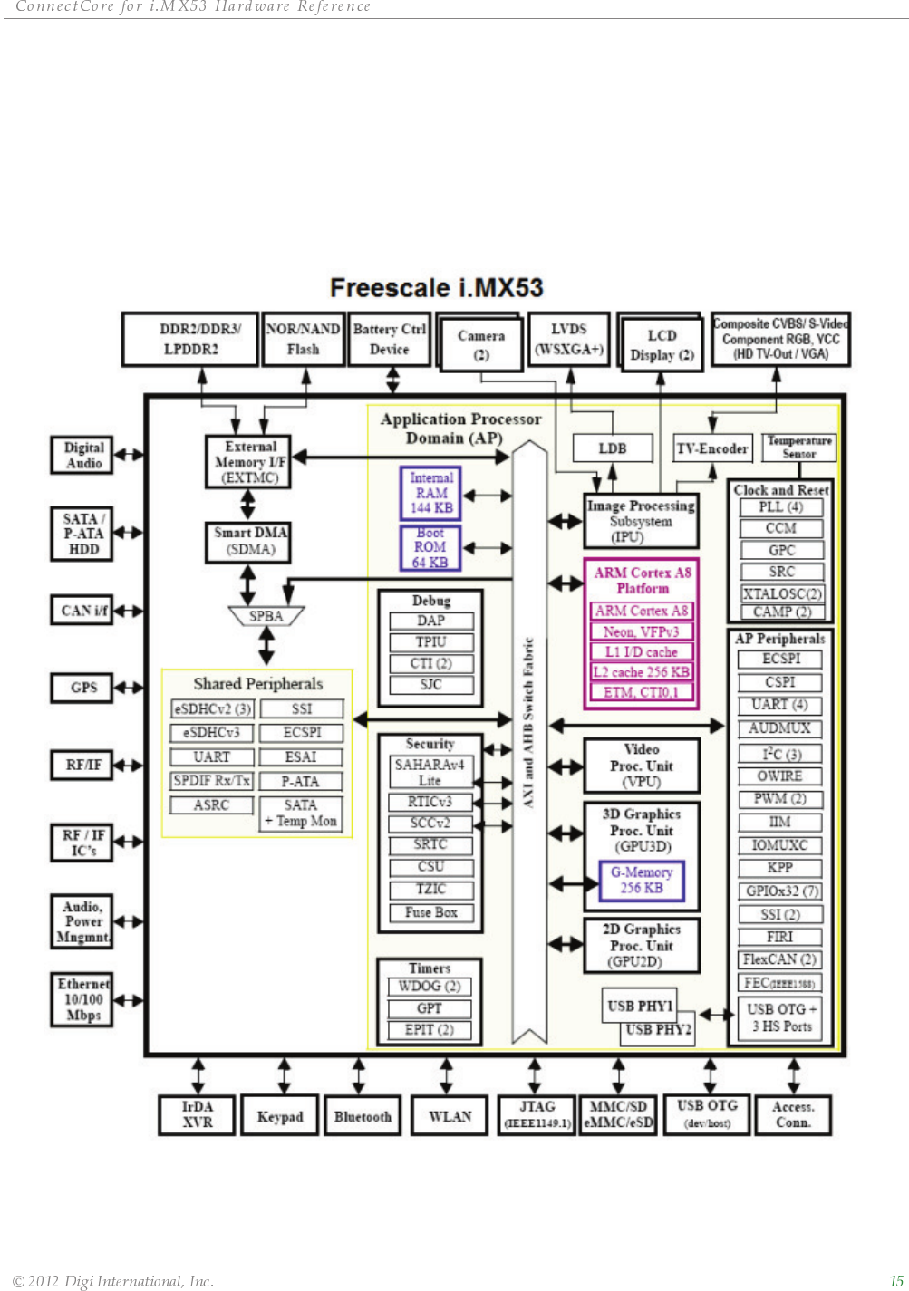
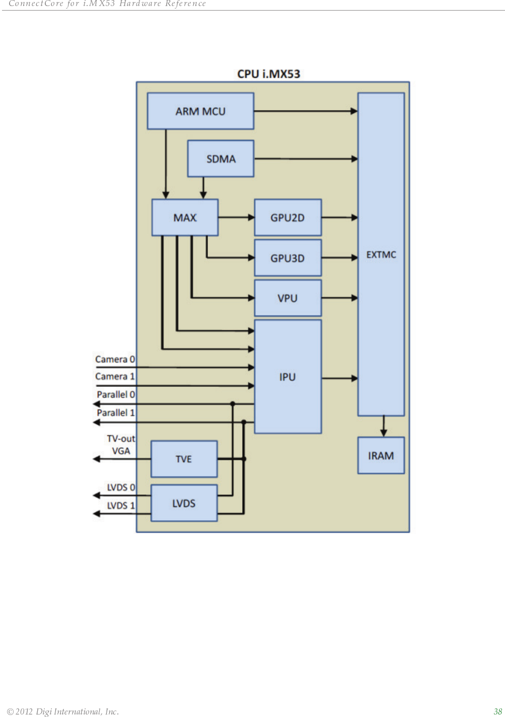
Block Diagram
The following figures show the block diagram of the Freescale i.MX535 CPU and the block
diagram of the ConnectCore for i.MX53 module.
CPU
ȱ ȱ ȱ ȱ ȱ ȱ
ȱ ȱ ȱ ȱ ȱȱȱȱȱ
Module
ConnectCore i.MX53
i
CPU i.MX53 Module
180-p
i
n Connector
Memory
Timers
ARM
C
Security
System Control
DDR2 Memory
Conguron
EMI
Interfces
IPU
ARM
C
ore
rt DMA
Interfes
Memory
C 3892
Eernet
HY
l
Buck SwitcesPower Mgmt
b
Controller
Regu
l
or10-
b
it ADC
Touc I/F Boost Switc
Ext
Power Supply
CPU I/FRTC
Accelerometer
180-pin Connector
DA9053 PMIC
ȱ ȱ ȱ ȱ ȱ ȱ
ȱ ȱ ȱ ȱ ȱȱȱȱȱ
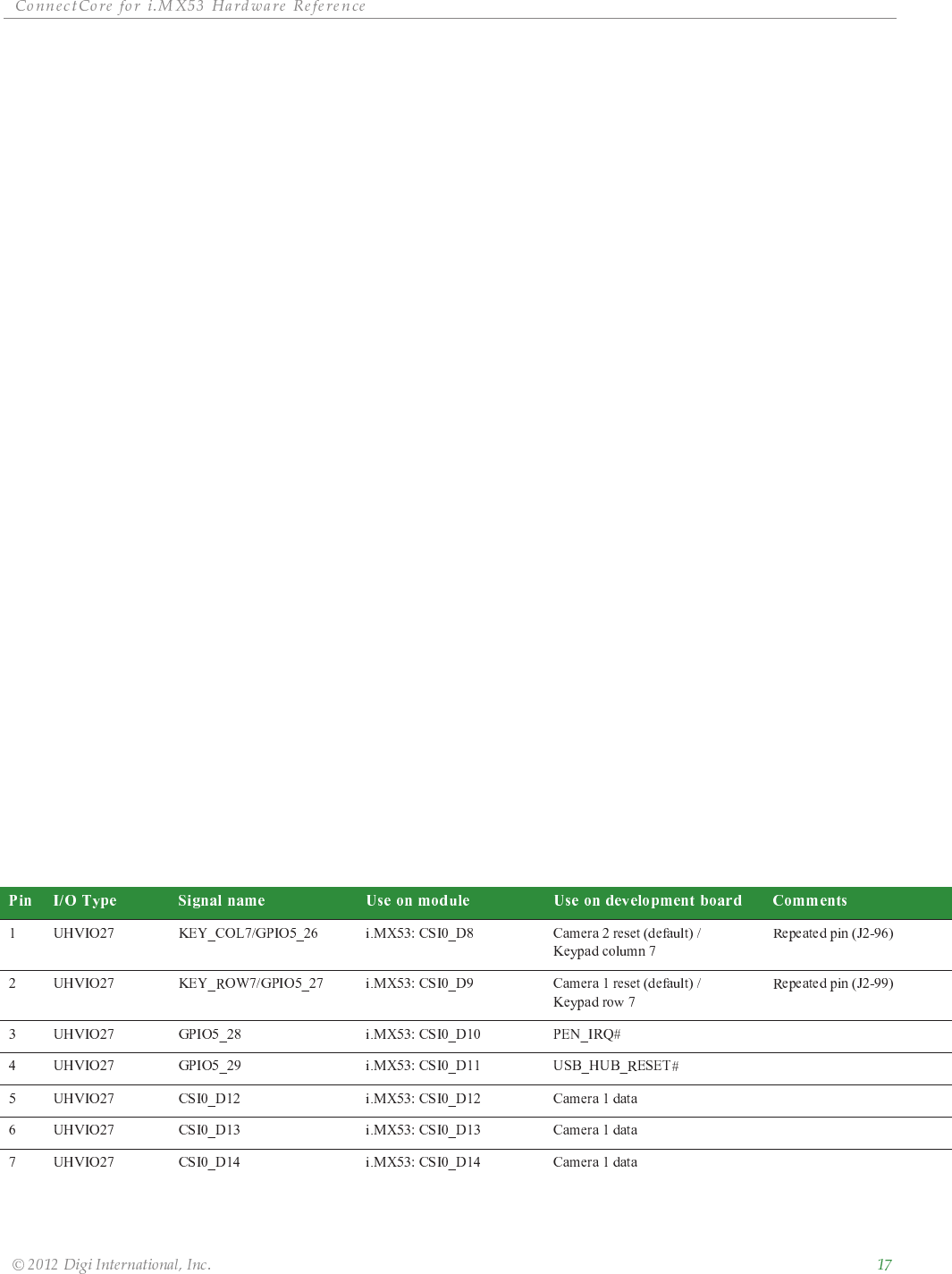
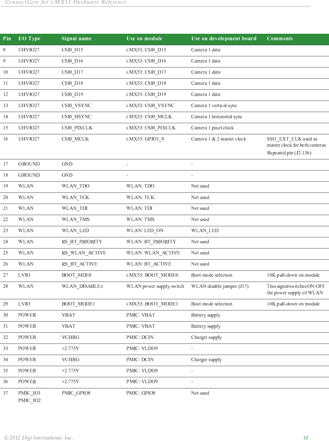
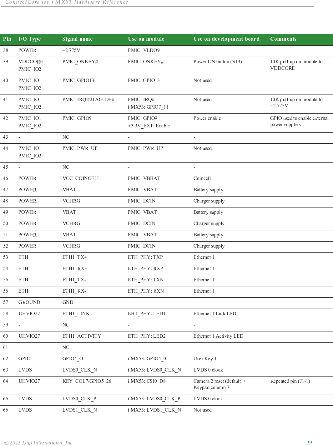
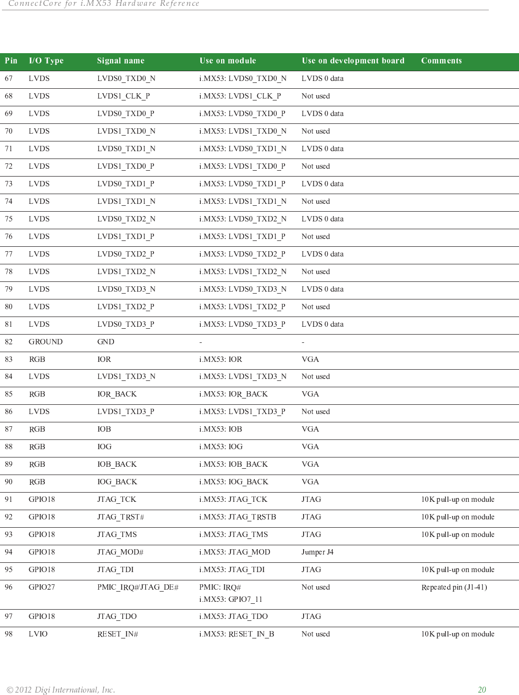
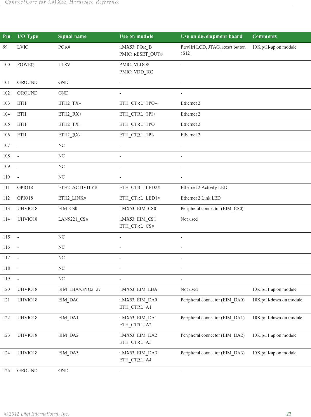
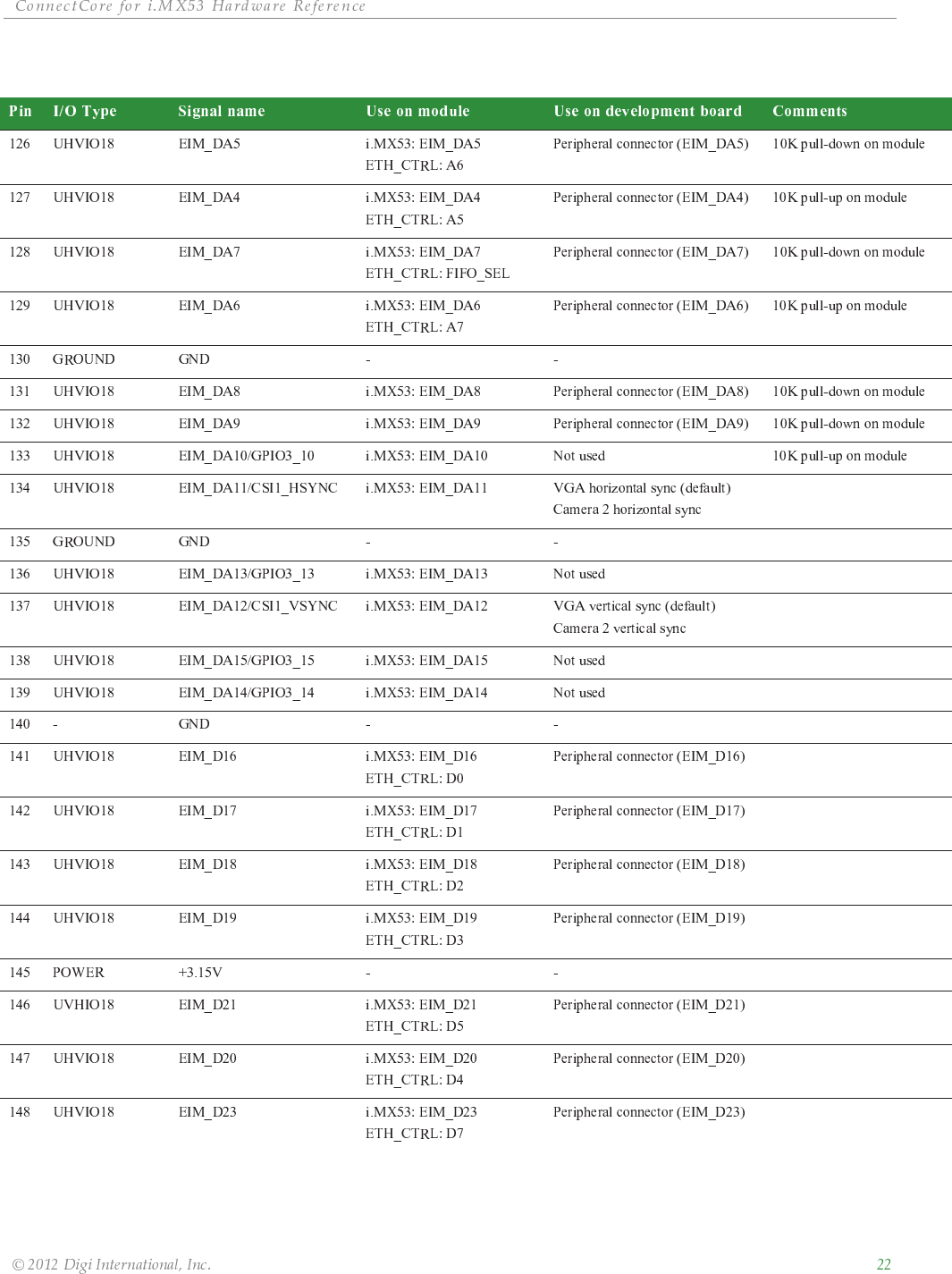
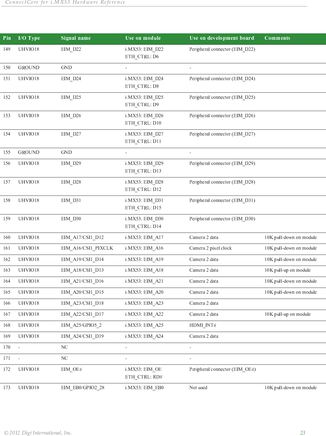
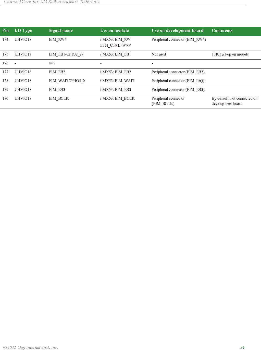
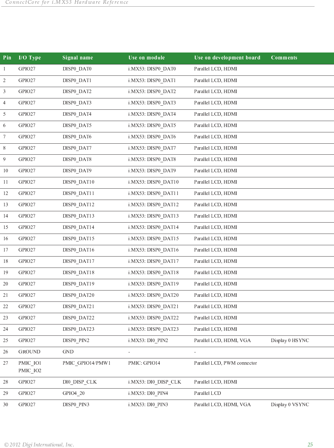
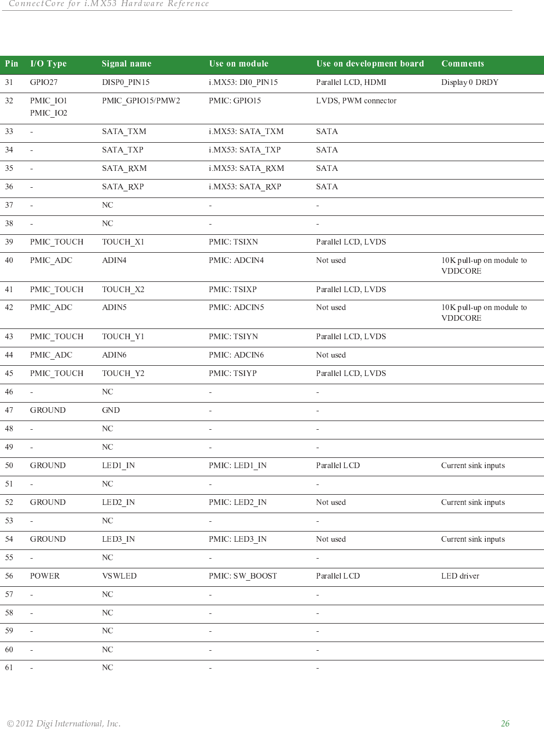
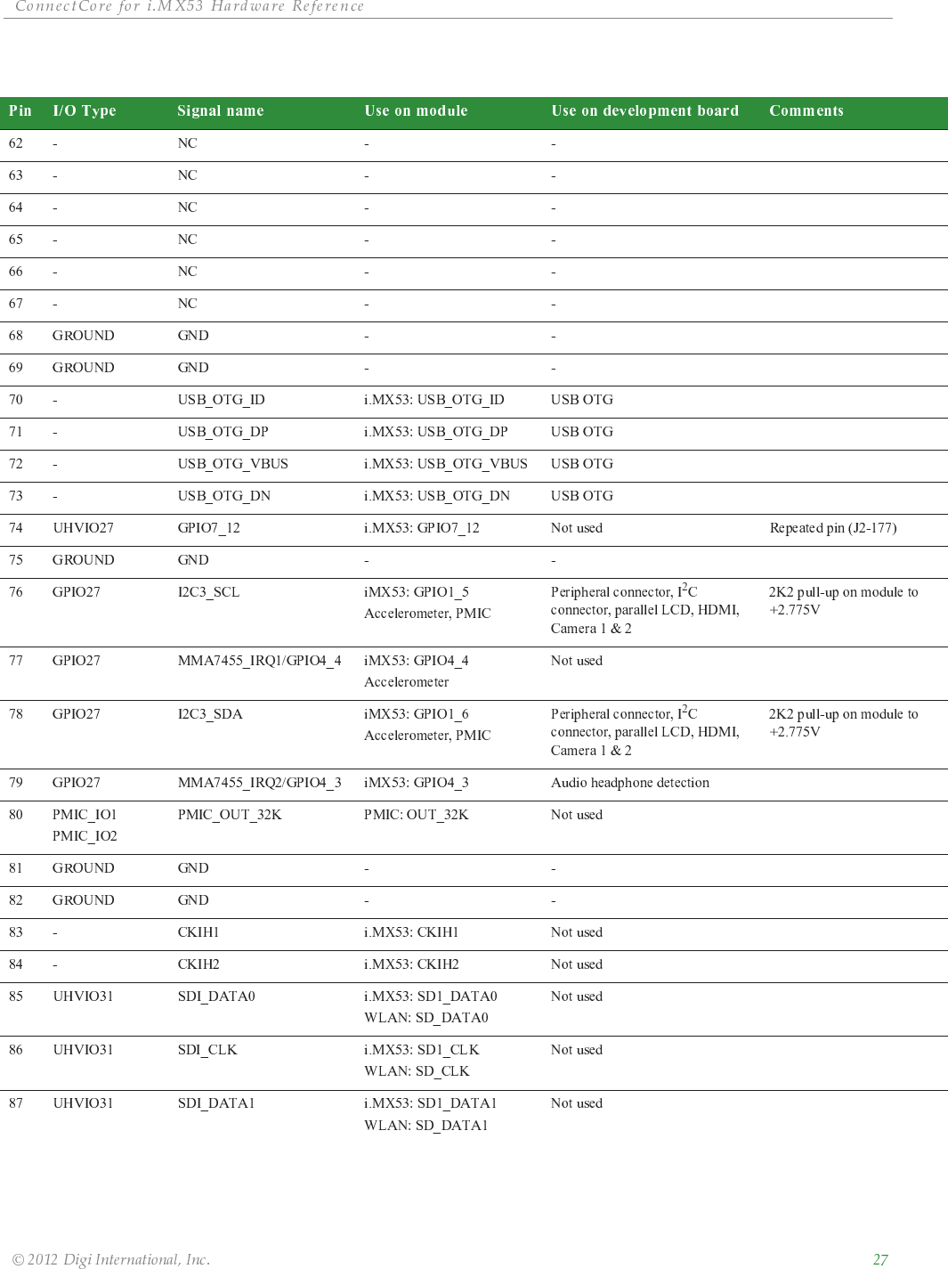
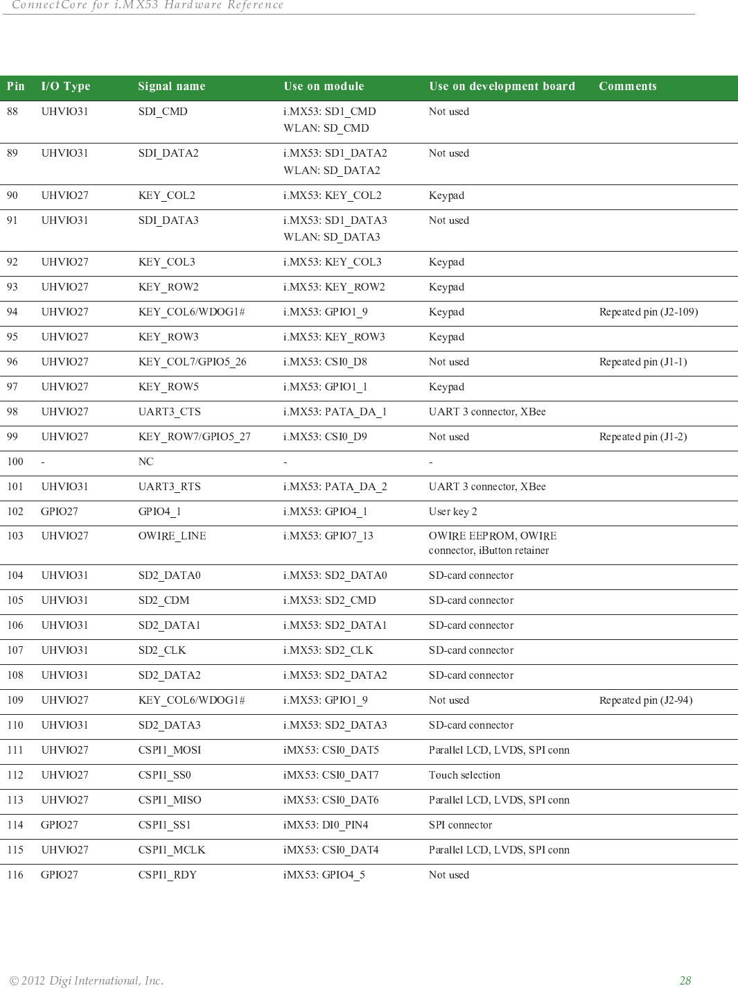
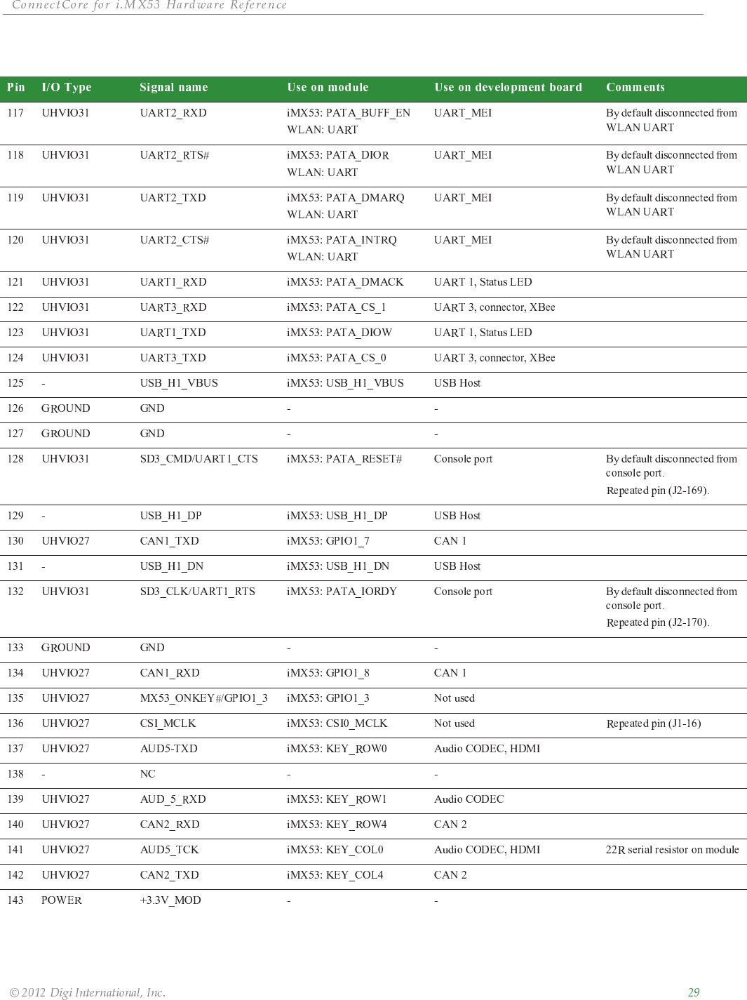
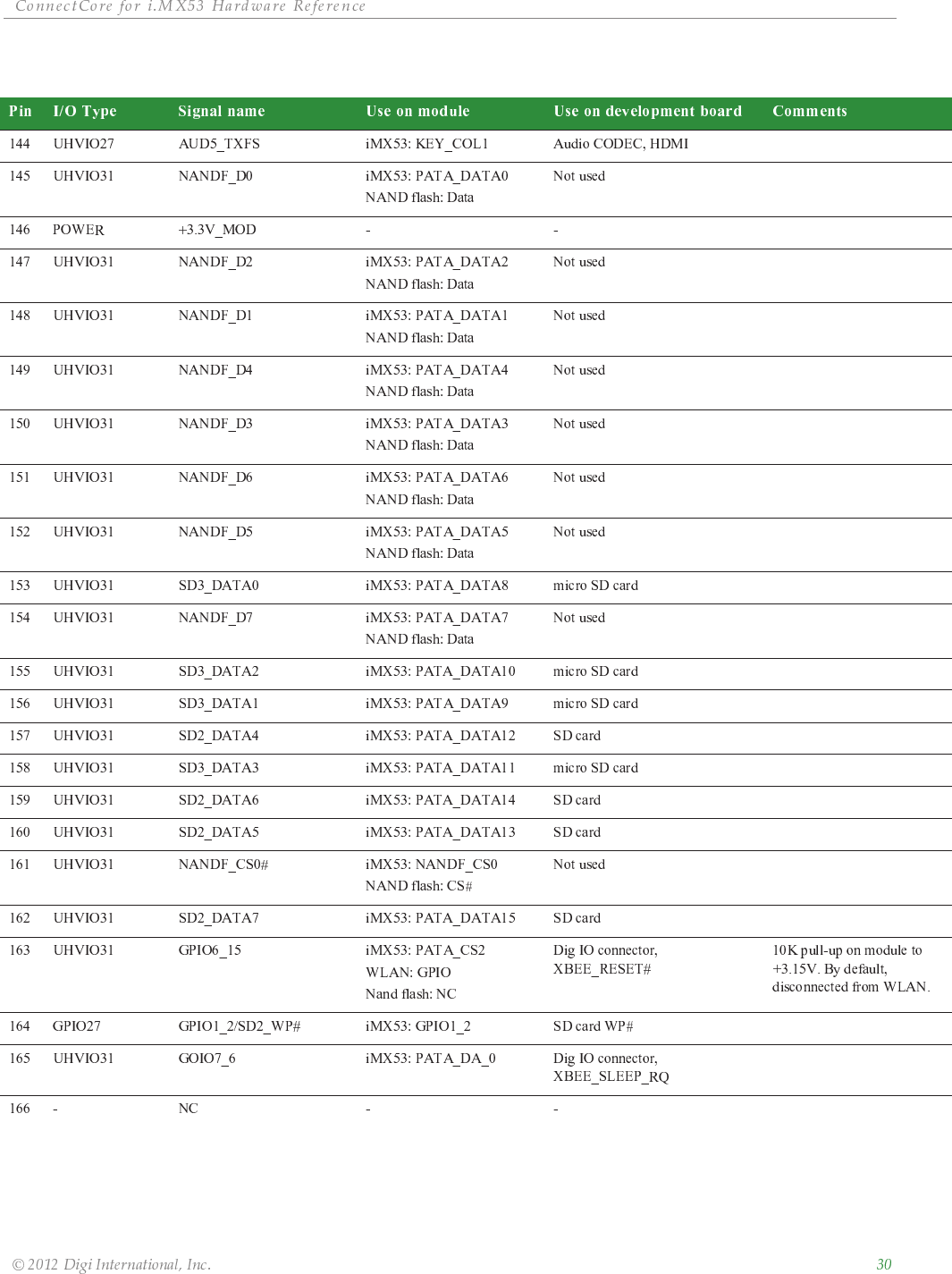
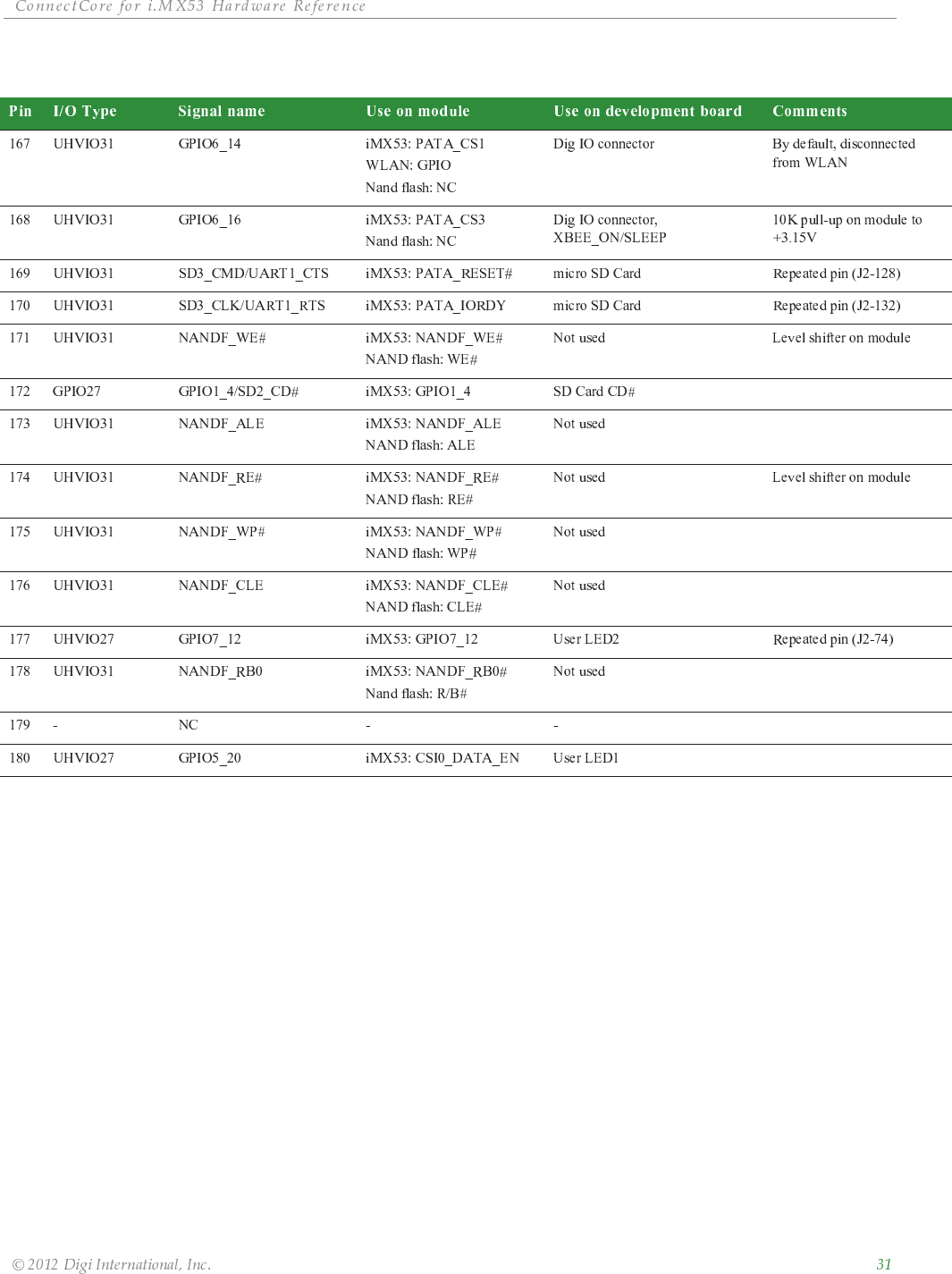
Module Pinout
The module has two 180-pin connectors, J1 and J2. The following tables describe each pin,
its properties, and its use on the module and development board. The DC parameters for
each I/O type are defined in the "I/O DC Parameters" section of Appendix A - Module
Specifications.
The ‘Use on module’ column shows the connection of the signals on the module. The format
of this column is component: pad_name, where ‘component’ indicates the connected
component on the module, and ‘pad_name’ indicates the corresponding component signal
(per datasheet).
Pinout Legend
# Low level active signal
NC Pin not connected on module
Pinout Definitions
GPIO - General Purpose IO
UHVIO - Ultra High Voltage IO
HSGPIO - High Speed GPIO
LVIO - Low Voltage IO (meaning 1.8V)
I/O Type descriptions can be read as follows:
18 - 1.8V logic level switching (for example, GPIO18)
27 - 2.775V logic level switching (for example, GPIO27)
31 - 3.15V logic level switching (for example, UHVIO31)
33 - 3.3V logic level switching (for example, UHVIO33)
J1 Pinout
ȱ ȱ ȱ ȱ ȱ ȱ
ȱ ȱ ȱ ȱ ȱȱȱȱȱ
ȱ ȱ ȱ ȱ ȱ ȱ
ȱ ȱ ȱ ȱ ȱȱȱȱȱ
ȱ ȱ ȱ ȱ ȱ ȱ
ȱ ȱ ȱ ȱ ȱȱȱȱȱ
ȱ ȱ ȱ ȱ ȱ ȱ
ȱ ȱ ȱ ȱ ȱȱȱȱȱ
ȱ ȱ ȱ ȱ ȱ ȱ
ȱ ȱ ȱ ȱ ȱȱȱȱȱ
ȱ ȱ ȱ ȱ ȱ ȱ
ȱ ȱ ȱ ȱ ȱȱȱȱȱ
ȱ ȱ ȱ ȱ ȱ ȱ
ȱ ȱ ȱ ȱ ȱȱȱȱȱ
ȱ ȱ ȱ ȱ ȱ ȱ
ȱ ȱ ȱ ȱ ȱȱȱȱȱ
J2 Pinout
ȱ ȱ ȱ ȱ ȱ ȱ
ȱ ȱ ȱ ȱ ȱȱȱȱȱ
ȱ ȱ ȱ ȱ ȱ ȱ
ȱ ȱ ȱ ȱ ȱȱȱȱȱ
ȱ ȱ ȱ ȱ ȱ ȱ
ȱ ȱ ȱ ȱ ȱȱȱȱȱ
ȱ ȱ ȱ ȱ ȱ ȱ
ȱ ȱ ȱ ȱ ȱȱȱȱȱ
ȱ ȱ ȱ ȱ ȱ ȱ
ȱ ȱ ȱ ȱ ȱȱȱȱȱ
ȱ ȱ ȱ ȱ ȱ ȱ
ȱ ȱ ȱ ȱ ȱȱȱȱȱ
ȱ ȱ ȱ ȱ ȱ ȱ
ȱ ȱ ȱ ȱ ȱȱȱȱȱ
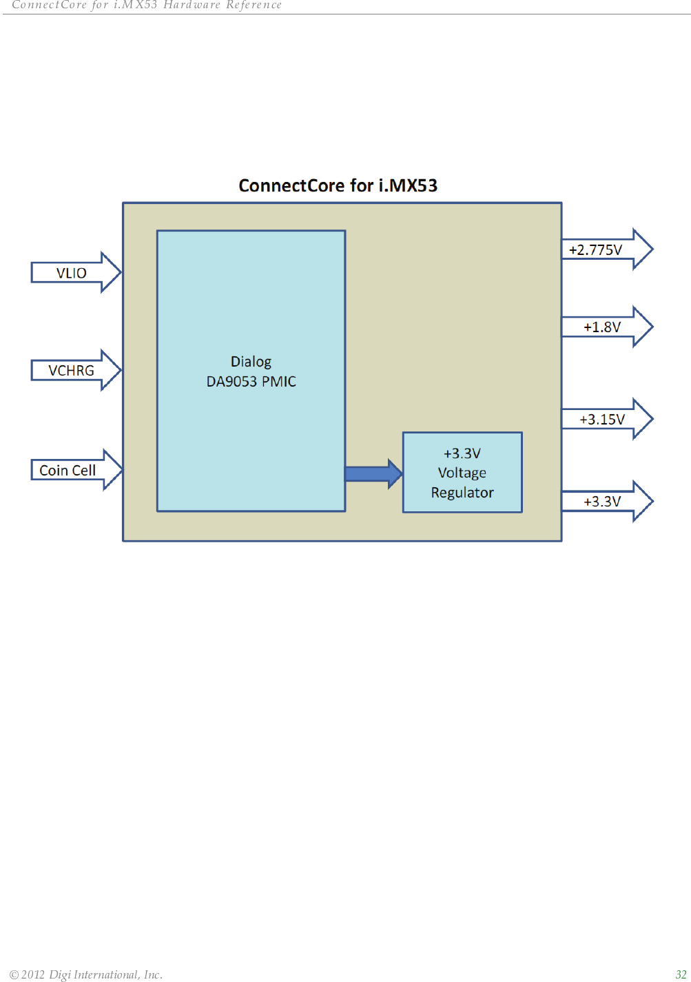
Power
Module Power Supplies
The following figure shows the power supply scheme of the ConnectCore for i.MX53 module.
Supply Inputs
The ConnectCore for i.MX53 module has the following supply inputs:
Battery input (VLIO)
Charger input (VCHRG)
Coin Cell input (VCC_COINCELL)
Battery input (VLIO)
The VLIO supply is used to generate all the voltage supplies needed by the ConnectCore for
i.MX53. The minimum voltage of VLIO (allowing the module to power up) is +3.4V. The
maximum voltage of VLIO is +4.8V.
This input is the recommended when only one of the two main power inputs (VLIO, VCHRG) is
used. The benefit of using this as the Main input is that power restrictions are relaxed and a
higher overall current may be drawn through this input. If this is used as the Main power
input, the other input VCHRG can be left disconnected. If this is the only power input used,
the supply must be rated to maintain the voltage on this input during times of peak demand
by the module.

ȱ ȱ ȱ ȱ ȱ ȱ
ȱ ȱ ȱ ȱ ȱȱȱȱȱ
Charger input (VCHRG)
The battery charger supply is used to charge rechargeable batteries, as well as to power up
the module when the battery is discharged or not connected. The minimum voltage of the
battery charger is +3.4V. The maximum voltage of the battery charger is +5.5V.
Whether this input is used depends on the Host Circuit. If a Lithium Ion secondary cell is
connected to VLIO this input is necessary, but the minimum voltage to allow the Lithium Ion
cell to charge means that the effective minimum input voltage rises to +4.5V. Note that the
i.MX53 module will still work when VCHRG is lower, but the battery will not charge. When
there is a Lithium Ion cell connected to VLIO and power is also applied to VCHRG, the current
needed by the i.MX53 module and anything that the module powers can be shared between
the two inputs. This allows a measurement of the average current to be taken and after
allowing a margin for variation and also for the charging of the battery, this figure can be
used as the amount needed at the VCHRG input. In this circumstance the peaks drawn by the
module are taken from the battery, thus allowing for a smaller power supply to power
VCHRG.
If there is no Lithium Ion secondary cell on VLIO, it is still allowed to use the VCHRG power
input as the Main input, in which case the VLIO input can be left disconnected. The benefit of
using this input as the Main input is that it has a wider input voltage range than VLIO. There
are some limitations on the amount of current that can be drawn (especially during power-
up), this may mean that Carrier boards for the module that use this power input alone may
need to have software controlled power features to prevent the load exceeding the current
capabilities. If this is the only power input used, the supply must be rated to maintain the
voltage on this input during times of peak demand by the module.
Coin Cell input (VCC_COINCELL)
A connection for a coin cell or supercap is provided at VCC_COINCELL. This power pin can
provide power to the RTC even without a connected main battery. If higher voltage is present
on the main battery or charger inputs, the main battery/charger will be used as a power
source instead.
There are three types of components that can be connected to this pin: Lithium coin cells
(Primary cell: non-rechargeable), Lithium coin cells (Secondary cell: rechargeable), and
Supercaps. When a Primary Lithium coin cell is connected, the charger must be turned off
and this pin is used strictly as an input. It is hazardous to attempt to charge Primary Lithium
cells as they may vent or explode. Secondary Lithium coin cells are only made available
directly to manufacturers of equipment that could use them, in that case they are normally
required to design their product to prevent the user gaining access to this part since there is
a danger to the user if by replacing it, they fit a primary type (the only sort that they are
likely to be able to source) into the charging circuit. When a Secondary Lithium coin cell is
used, both the charging current and the termination voltage are programmable. When a
Supercap is used, both the charge current and termination voltage should be set to the
maximum values.
The advantage of using a Primary Lithium coin cell is that the energy density usually allows
years of service since the self discharge rate is low. The advantage of using a Secondary
Lithium coin cell is that the self discharge rate is usually sufficient to allow a few months of
support for the RTC before it will need recharging. The advantage of the Supercap is that it is
intrinsically safe and can out-last the Primary Lithium coin cell option, however the self
discharge rate is high meaning that a 1F capacitor at 25° C is likely to support the RTC for
approximately 5 to 10 days.

ȱ ȱ ȱ ȱ ȱ ȱ
ȱ ȱ ȱ ȱ ȱȱȱȱȱ
A programmable constant charge current charger with a programmable top-off charging
voltage is provided for charging of Secondary Lithium-Manganese coin cell batteries and
super capacitors. Charging current is programmable from 100uA to 6mA. Termination voltage
is programmable from +1.1 to +3.1V.
The minimum voltage of the coin cell supply is +2V. The maximum voltage of the coin cell
supply is +3.6V.
Supply Outputs
The ConnectCore for i.MX53 module provides the following supply outputs:
+3.3V
+2.775V
+1.8V
+3.15V
+3.3V
The ConnectCore for i.MX53 module has a DC/DC converter to generate a +3.3V supply. This
supply is used on the module to power the WLAN interface, the Ethernet PHY and the
Ethernet Controller.
This power regulator can be enabled/disabled by software to save power when the module is
in the low power modes. The maximum current provided by this regulator is 1A.
The current available to supply off-module components is 400mA for the wireless variants of
the ConnectCore for i.MX53, and 800mA for the wired-only variant of the ConnectCore for
i.MX53. If the module is powered from the charger, the maximum charger current limit
(1800mA) may limit the current available to supply off-module components.
+2.775V
This supply is generated by LDO4 of the DA9053 PMIC. This supply is used on the module to
power the CPU peripherals, the Ethernet PHY, the accelerometer and the CPU image
processing unit. The maximum current provided by this supply is 150mA.
The current available to supply off-module components is 80mA.
+1.8V
This supply is generated by LDO8 of the DA9053 PMIC. This supply is used on the module to
power the External Interface Module (EIM), the JTAG interface, the touch screen controller
and the Ethernet controller. The maximum current provided by this supply is 200mA.
The current available to supply off-module components is 100mA.
+3.15V
This supply is generated by LDO6 of the DA9053 PMIC. This supply is used in the module to
power the NAND flash interface, the SD interfaces and the PATA controller. The maximum
current provided by this supply is 150mA.
The current available to supply off-module components is 100mA.
ȱ ȱ ȱ ȱ ȱ ȱ
ȱ ȱ ȱ ȱ ȱȱȱȱȱ
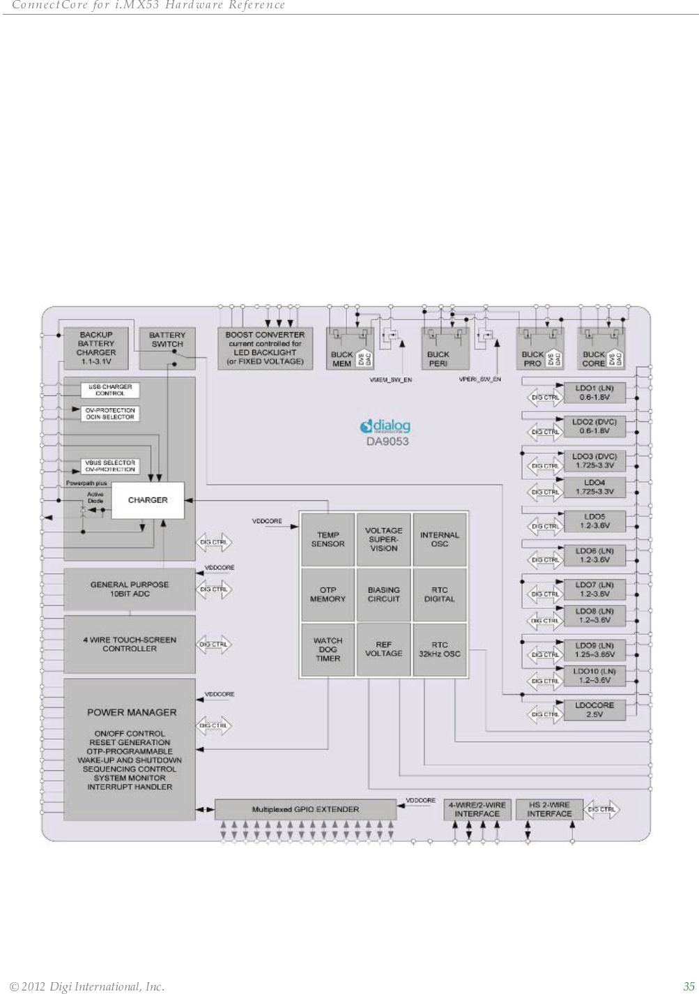
DA9053 Power Management
The ConnectCore for i.MX53 module integrates a Dialog DA9053 Power Management chip. This
chip provides reference and supply voltages for the ConnectCore for i.MX53 processor as well
as for the peripheral devices.
The DA9053 provides four buck switchers and ten low dropout regulators. The start-up of
DA9053 supplies is performed with a configurable sequencer. The DA9053 also provides a
battery charger that supports current/voltage charging at currents up to 1.25A. Other
interfaces as touch screen, general purpose 10bit ADC and PWM are also included on the
DA9053.
The following figure shows a block diagram of the DA9053.
ȱ ȱ ȱ ȱ ȱ ȱ
ȱ ȱ ȱ ȱ ȱȱȱȱȱ
Memory
Overview
The i.MX53 processor has an External Memory Controller (EXTMC) that services all the
external memory access requests. The EXTMC provides the arbitration interface and different
external memory controllers in order to support several memory devices:
M4IF – Multi Master Multi Memory Interface
ESDRAMC – Enhanced DDR memory controller
NFC – NAND flash memory controller
EIM – SRAM/PSRAM/NOR/NOR flash memory controller
DDR2 SDRAM Memory
The ConnectCore for i.MX53 module provides up to 2GB of DDR2-800 SDRAM memory. On the
module in the development kits four 16-bit, 128Mbit, DDR2-800 chips, configured as two
banks of 32-bits of 128Mbits DDR2-800 memory are used.
NAND Flash Memory
The ConnectCore for i.MX53 module provides 8GB of NAND flash memory. On the module in
the development kits a 512MByte, 2Kbyte page, NAND flash chip is used. This NAND flash
device is connected to NAND flash Chip Select 0.
The NAND flash controller signals are available on the module connectors.
External Interface Module (EIM)
The External Interface Module (EIM) is used on the ConnectCore for i.MX53 module to control
the Ethernet Controller. This device is connected to EIM Chip Select 1.
The EIM signals are available on the module connectors.
System Boot
The ConnectCore for i.MX53 boot process begins at Power On Reset when the hardware reset
logic forces the ARM core to begin execution starting from the on-chip boot ROM. Boot ROM
code uses the state of the internal register BOOT_MODE[1:0] as well as the state of various
eFUSEs and/or GPIO settings to determine the boot flow behavior of the module.
The ConnectCore for i.MX53 supports the following boot modes:
Internal boot
– The module boots from the internal ROM
– Program Image loaded from the chosen boot device
– Boot flow controlled by GPIO and eFUSE (GPIO overrides eFUSE settings)
– Supports a secure boot using HAB

ȱ ȱ ȱ ȱ ȱ ȱ
ȱ ȱ ȱ ȱ ȱȱȱȱȱ
Boot from fuses
– Same as internal boot but GPIO boot override pins are ignored
Serial Downloader
– Supports UART and USB
The ConnectCore for i.MX53 supports the following boot devices:
NOR flash with External Interface Module (EIM), located on CS0, 16-bits bus width
One NAND flash with EIM, located on CS0, 16-bits bus width
NAND flash
SD/MMC
Parallel ATA (PATA)/Serial ATA (SATA) HDD
Serial ROM devices (SPI and I2C EEPROM)
Audio Subsystem
The audio subsystem provided by the ConnectCore for i.MX53 consists of the SSI, SPDIF and
the AUDMUX blocs. In addition, the IOMUXC must be configured for appropriate signal
directions.
Video Subsystem
The ConnectCore for i.MX53 has a video subsystem that includes the following modules:
Video Processing Unit (VPU): a multi-standard video/image codec
Two Graphics Processing Units (GPUs): one for accelerating 3D graphics (OpenGL/ES),
and one for accelerating vector graphics (OpenVG and 2D graphics BitBLT)
Image Processing Unit (IPU): providing connectivity to cameras and displays, related
processing, synchronization and control
Display interface bridge: providing optional translation from the digital display
interface supported by the IPU to other interfaces:
– TV encoder (TVE) bride: composite, S-video, component and VGA interfaces
– LVDS bridge: up to two LVDS interfaces
The following figure on the next page shows the block diagram of the Video Subsystem:
ȱ ȱ ȱ ȱ ȱ ȱ
ȱ ȱ ȱ ȱ ȱȱȱȱȱ
ȱ ȱ ȱ ȱ ȱ ȱ
ȱ ȱ ȱ ȱ ȱȱȱȱȱ
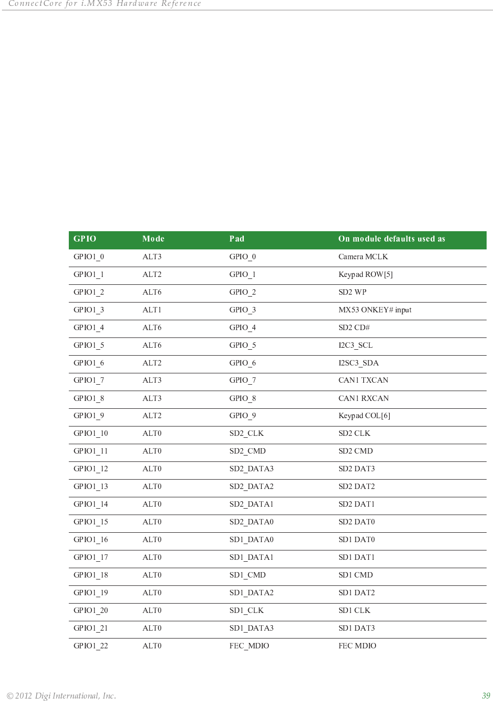
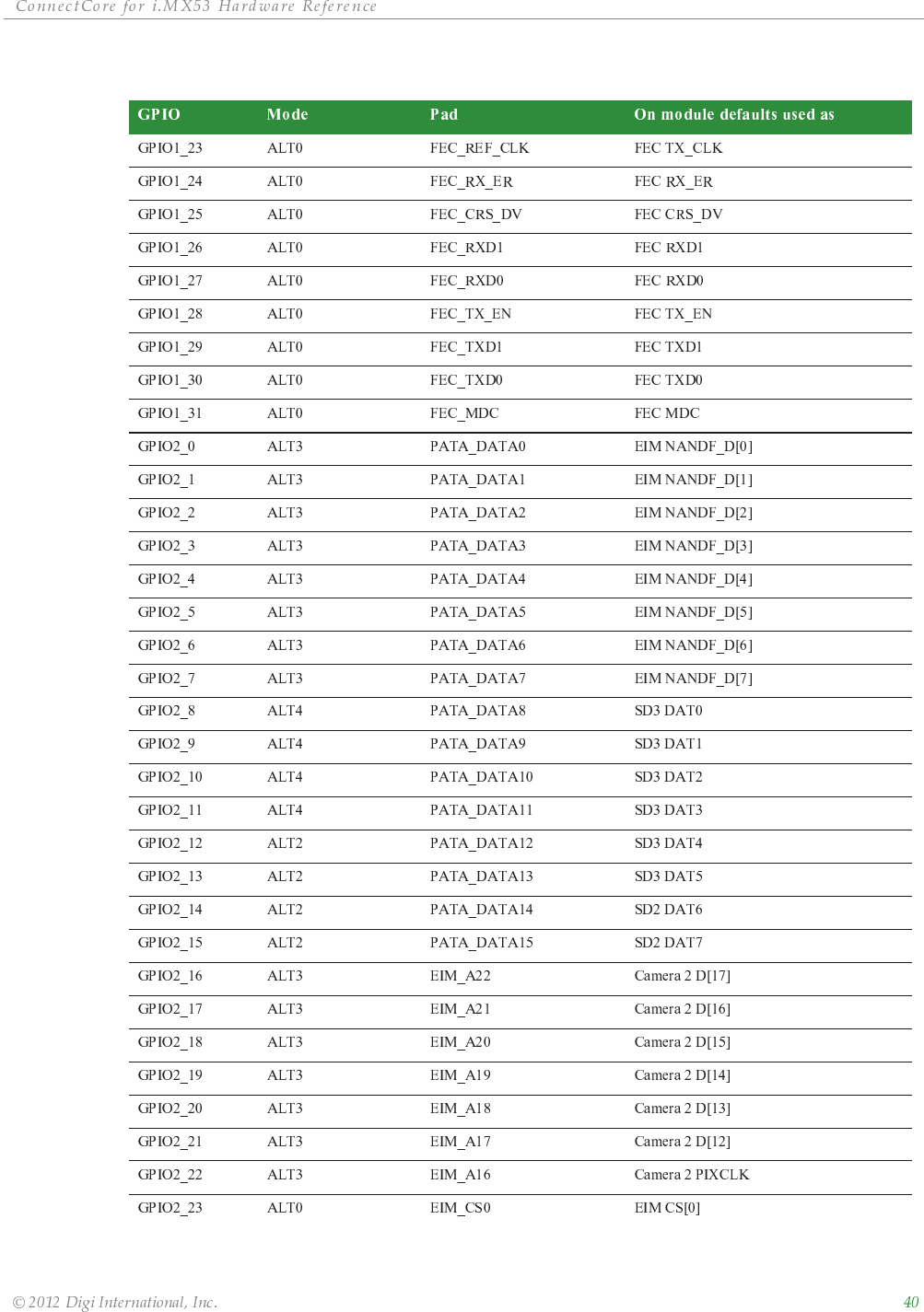
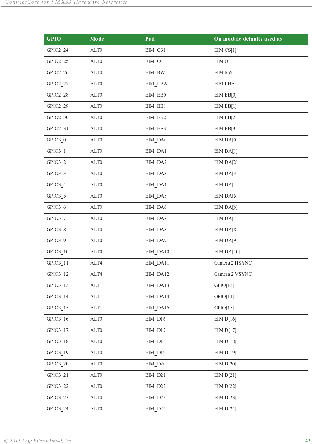
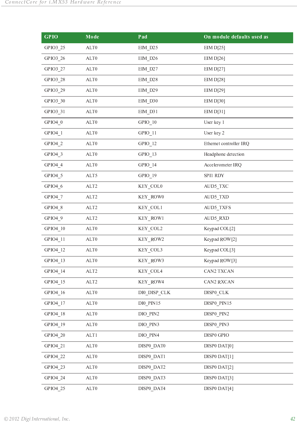
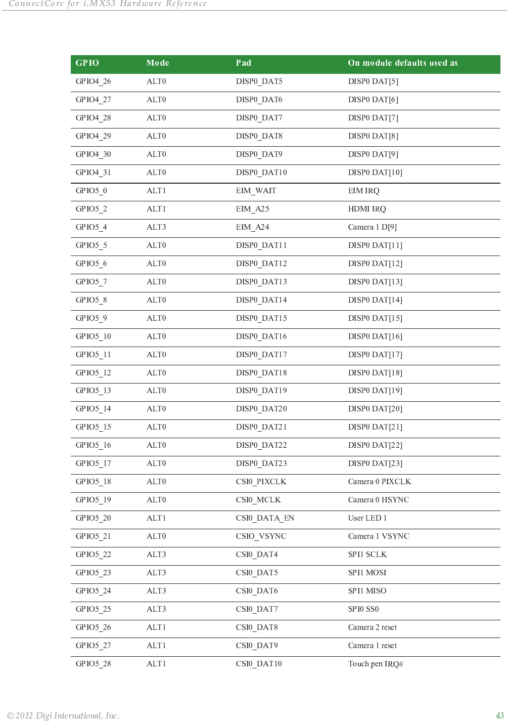
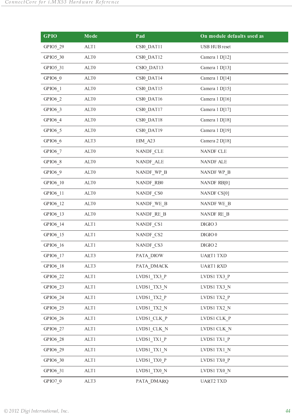
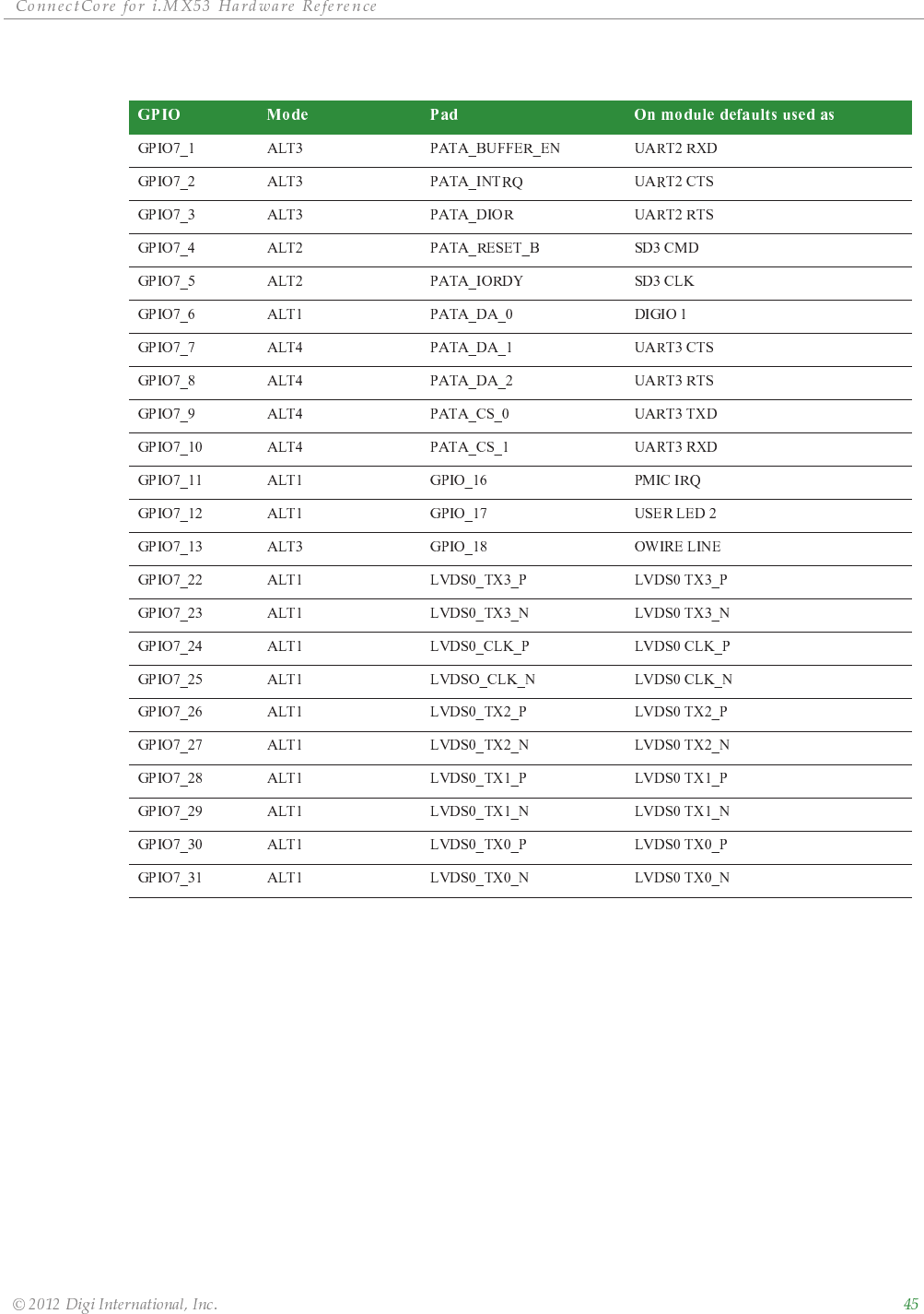
Multiplexed GPIO
GPIO Multiplexing Table
The ConnectCore for i.MX53 has seven GPIO banks. Each bank provides up to 32 bidirectional
general purpose input and output signals.
The GPIO pins are multiplexed with other functions on the module. The IOMUX controller
allows the configuration of the pin functions (ALT Mode) and other options (pull-up, keeper,
etc).
The table below shows the default configuration of the GPIO pins, the name of the Pad and
the default use on the ConnectCore for i.MX53 module. For a detailed description of all the
muxing options for each pin, please refer to the Freescale i.MX53 Reference Manual
(IMX53RM).
ȱ ȱ ȱ ȱ ȱ ȱ
ȱ ȱ ȱ ȱ ȱȱȱȱȱ
ȱ ȱ ȱ ȱ ȱ ȱ
ȱ ȱ ȱ ȱ ȱȱȱȱȱ
ȱ ȱ ȱ ȱ ȱ ȱ
ȱ ȱ ȱ ȱ ȱȱȱȱȱ
ȱ ȱ ȱ ȱ ȱ ȱ
ȱ ȱ ȱ ȱ ȱȱȱȱȱ
ȱ ȱ ȱ ȱ ȱ ȱ
ȱ ȱ ȱ ȱ ȱȱȱȱȱ
ȱ ȱ ȱ ȱ ȱ ȱ
ȱ ȱ ȱ ȱ ȱȱȱȱȱ
ȱ ȱ ȱ ȱ ȱ ȱ
ȱ ȱ ȱ ȱ ȱȱȱȱȱ
Interfaces
1-Wire
The ConnectCore for i.MX53 provides a 1-Wire interface to communicate with 1-Wire devices
such as EEPROMs, secure memory and sensors. The required protocol for accessing the
generic 1-Wire device is defined by Maxim.
The 1-Wire interfaces offer the following capabilities:
Performs the 1-Wire bus protocol to communicate with an external 1-Wire device.
Provides a clock divider to generate a 1-Wire bus reference clock.
Supports byte transfers with optional interrupts for more efficient programming.
Provides a search ROM accelerator mode to speed the search ROM protocol.
Accelerometer
The module provides a three axis digital output accelerometer. This device is connected to
the CPU through the I2C bus.
The accelerometer offers the following:
User assigned registers for offset calibration
Programmable threshold interrupt output
Level detection for motion recognition (shock, vibration, freefall)
Pulse detection for single or double pulse recognition
Selectable sensitivity (±2g, ±4g, ±8g) for 8-bit mode
ȱ ȱ ȱ ȱ ȱ ȱ
ȱ ȱ ȱ ȱ ȱȱȱȱȱ
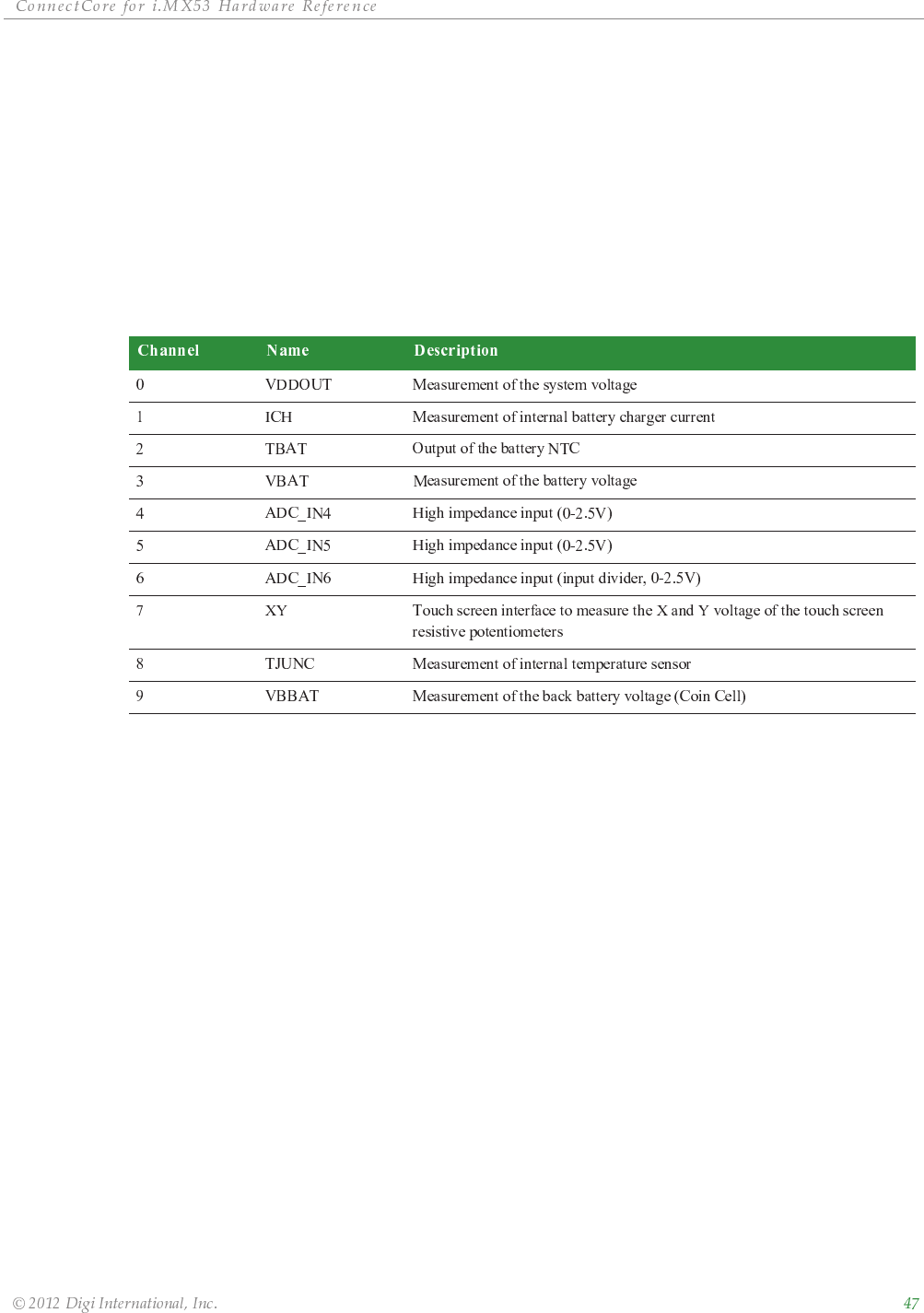
ADC and Touch Screen
The module provides an Analogue to Digital Converter (ADC) and Touch Screen Interface. The
ADC/Touch interface is part of the integrated DA9053 PMIC.
The ADC has a 10 bit resolution and a track and hold circuitry combined with an analog input
multiplexer. The analog multiplexer allows conversion of up to 10 different inputs.
The track and hold circuit ensures stable input voltages at the input of the ADC during the
conversion.
The following table shows the ADC channel assignments:
CAN
The ConnectCore for i.MX53 provides two FlexCAN controllers implementing the CAN protocol
according to the CAN 2.0B protocol specification. The CAN block includes two embedded
memories, one for storing Message Buffers and another one for storing Rx Individual Mask
Registers.
The FlexCAN controllers include these distinctive features:
Full Implementation of the CAN protocol specification
– Standard data and remote frames
– Extended data and remote frames
– Zero to eight bytes data length
– Programmable bit rate up to 1 Mb/sec
– Content-related addressing
Deterministic behavior and increased reliability of FlexCAN
Flexible Message Buffers of zero to eight bytes data length
Each Message Buffer configurable as Rx or Tx, all supporting standard and extended
messages

ȱ ȱ ȱ ȱ ȱ ȱ
ȱ ȱ ȱ ȱ ȱȱȱȱȱ
Individual Rx Mask Registers per Message Buffer
Includes 1056 bytes (64 Mbytes) of RAM used for Message Buffer storage
Includes 256 bytes (64 Mbytes) of RAM used for individual Rx Mask Registers
Full featured Rx FIFO with storage capacity for 6 frames and internal pointer handling
Powerful Rx FIFO ID filtering, capable of matching incoming IDs against either 8
extended, 16 standard or 32 partial (8 bits) IDs, with individual masking capability
Selectable backwards compatibility with previous CAN version
Programmable clock source to the CAN Protocol Interface, either bus clock or crystal
oscillator
Unused message buffer and Rx Mask Register space can be used as general purpose
RAM space
Listen only mode capability
Programmable loop-back mode supporting self-test operation
Programmable transmission priority scheme: lowest ID, lowest buffer number or
highest priority
Time Stamp based on 16-bit free-running timer
Global network time, synchronized by a specific message
Maskable interrupts
Independent of the transmission medium (an external transceiver is assumed)
Short latency time due to an arbitration scheme for high-priority messages
Low power modes, with programmable wake up on bus activity
Configurable Glitch filter width to filter the noise on CAN bus when waking up
Clock Amplifier (CAMP)
The ConnectCore for i.MX53 provides two inputs connected to a clock amplifier. The clock
amplifier converts a square wave/sinusoidal input of frequency range 8-40 MHz, into a +1.8V
rail to rail square wave.
The input to the CAMP is internally AC coupled. No external coupling is required.
The outputs of the CAMP are connected to the Clock Control Module (CCM) of the
ConnectCore for i.MX53.

ȱ ȱ ȱ ȱ ȱ ȱ
ȱ ȱ ȱ ȱ ȱȱȱȱȱ
Configurable SPI (CSPI)
The ConnectCore for i.MX53 module provides one Configurable SPI (CSPI) interface that can
be configured in either master or slave mode. The CSPI contains an 8 x 32 receive buffer
(RXFIFO) and an 8 x 32 transmit buffer (TXFIFO).
Key features of the CSPI include:
Full-duplex synchronous serial interface
Master/Slave configurable
Four Chip Select (SS) signals to support multiple peripherals
Transfer continuation function allows unlimited length data transfers
32-bit wide by 8-entry FIFO for both transmit and receive data
Polarity and phase of the Chip Select (SS) and SPI Clock (SCLK) are configurable
Direct Memory Access (DMA) support
Max operation frequency up to one quarter of the reference clock frequency
Digital Audio MUX (AUDMUX)
The Digital Audio Multiplexer (AUDMUX) provides a programmable interconnect device for
voice, audio, and synchronous data routing between host serial interfaces, such as SSI, and
peripheral serial interfaces-that is, audio and voice codecs.
The AUDMUX includes two types of interfaces. Host ports connect to the processor serial
interfaces, and peripheral ports connect to off-chip audio devices. A desired connectivity is
achieved by configuring the appropriate host and peripheral ports.
The AUDMUX provides flexible, programmable routing of the on-chip serial interfaces to and
from off-chip audio devices. The AUDMUX routes audio data but does not decode or process
audio data itself.
Enhanced Configurable SPI (ECSPI)
The ConnectCore for i.MX53 module provides two Enhanced Configurable SPI (ECSPI)
interfaces that can be configured in either master or slave mode. The ECSPI contains a
64 x 32 receive buffer (RXFIFO) and a 64 x 32 transmit buffer (TXFIFO).
Key features of the ECSPI include:
Full-duplex synchronous serial interface
Master/Slave configurable
Four Chip Select (SS) signals to support multiple peripherals
Transfer continuation function allows unlimited length data transfers
32-bit wide by 64-entry FIFO for both transmit and receive data
32-bit wide by 16-entry FIFO for HT message data
Polarity and phase of the Chip Select (SS) and SPI Clock (SCLK) are configurable

ȱ ȱ ȱ ȱ ȱ ȱ
ȱ ȱ ȱ ȱ ȱȱȱȱȱ
Direct Memory Access (DMA) support
Max operation frequency up to the reference clock frequency
Ethernet 1
The ConnectCore for i.MX53 provides a Fast Ethernet Controller (FEC) designed to support
both 10 and 100 Mbps Ethernet/IEEE 802.3 networks. A low-power 10/100 Ethernet PHY
(SMSC LAN8710A) is integrated on the module.
The module does not provide a transformer and Ethernet connector.
The PHY address on the MII bus is 0x7 (0b00111).
The module also provides two status signals for activity and link LEDs.
Ethernet 2
The ConnectCore for i.MX53 module can provide an optional high-performance 10/100Mbit
Ethernet controller (SMSC LAN9221) with integrated MAC and PHY as a second Ethernet port.
Key features of the second Ethernet controller:
Embedded 16 Kbyte FIFO for packet buffers
Support burst-mode read for highest performance applications
Configurable interrupt pin with programmable hold-off timer
Compatible with IEEE 802.3, 802.3u standards
Integrate Fast Ethernet MAC/PHY transceiver in one chip
10Mbps and 100Mbps data rate
Full and half duplex operations
10/100Mbps Auto-negotiation operation
Twisted pair crossover detection and auto-correction (HP Auto-MDIX)
EEE 802.3x flow control for full-duplex operation
Wake-on-LAN capabilities:
LED pins for various network activity indications
The Ethernet controller is connected to EIM_CS1#. Its programmable polarity interrupt
output is connected to the signal GPIO4_2.
The module does not have a transformer and Ethernet connector.
The module provides two status signals for activity and link LEDs.

ȱ ȱ ȱ ȱ ȱ ȱ
ȱ ȱ ȱ ȱ ȱȱȱȱȱ
External Interface Module (EIM)
The ConnectCore for i.MX53 module provides access to the External Interface Module (EIM) of
the i.MX53 processor. The EIM allows interfacing devices external to the ConnectCore for
i.MX53, including generation of chip selects, clock and control for external peripherals and
memory. It provides asynchronous access to devices with SRAM-like interface and
synchronous access to devices with NOR-flash-like or PSRAM-like interface.
Key features of the External Interface Module:
Support for multiplexed address/data bus operations x16 and x32
Programmable data port size of each Chip select (x8, x16 and x32)
Up to 6 Chip select with selectable Write Protection for each Chip Select
Read and write control lines
26-bit address bus
2x byte enable signals
Asynchronous accesses with programmable setup and hold times for control signals
Support for Asynchronous page mode accesses (x16 and x32 port size)
Independent synchronous Memory Burst Mode support for Nor-flash and PSRAM
memories (x16 and x32 port size)
Support for Big Endian and Little Endian operation modes per access
General Purpose Input/Output (GPIO)
The GPIO peripheral provides dedicated general-purpose pins that can be configured as
either inputs or outputs. When configured as an output, it is possible to write to an internal
register to control the state driven on the output pin. When configured as an input, it is
possible to detect the state of the input by reading the state of an internal register.
In addition, the GPIO peripheral can produce CORE interrupts.
Each GPIO input has a dedicated edge-detect circuit which can be configured through
software to detect rising edges, falling edges, logic low-levels or logic high-levels on the
input signals. The outputs of the edge detect circuits are optionally masked by setting the
corresponding bit in the interrupt mask register.
The GPIO includes the following features:
General purpose input/output logic capabilities:
– Drives specific data to output using the data register (GPIO_DR)
– Controls the direction of the signal using the GPIO direction register (GPIO_GDR)
– Enables the core to sample the status of the corresponding inputs by reading the pad
sample register (GPIO_PSR).

ȱ ȱ ȱ ȱ ȱ ȱ
ȱ ȱ ȱ ȱ ȱȱȱȱȱ
GPIO interrupt capabilities:
– Supports up to 32 interrupts
– Identifies interrupt edges
– Generates three active-high interrupts to the ConnectCore for i.MX53 interrupt
controller
Graphics Processing Unit 2D (GPU2D)
The 2D graphics processing unit is an embedded 2D and vector graphics accelerator. The
GPU2D is divided into two segments. The first accelerates 2D bitmap graphics operations.
The second one accelerates vector graphics rendering with anti-aliasing polygon rasterizer.
Key features of the GPU2D:
Frame buffer size support up to 2048x2048
Linear and block-based (4x4 pixels) frame buffer modes
Fast buffer clears
Support for OpenVG render to Image
Main features of the 2D bitmap graphics unit:
BitBlt (surface-to-surface copy)
Block fill
Internal 32-bit color precision
Supports three source bitmaps for separate mask/pattern/alpha bitmap support plus
reading destination for ROP, blend and color key operations
Supports masking source coordinates for wrapping patterns
Supports inverting mask and alpha values from source
Supports destination rotation by 0/90/180/270 degrees
Supports programmable blending with optional alpha un-premultiply
Supports color keying by source and destination colors, with optional ignoring of alpha
channel
Supports one scissor rectangle for destination coordinates
Dithering (ordered)
Color component masking
sRGB reads and writes
BitBlt with scaling, bilinear filtering with texture lookups, programmable filter
kernels possible with the programmable Pixel processor

ȱ ȱ ȱ ȱ ȱ ȱ
ȱ ȱ ȱ ȱ ȱȱȱȱȱ
Key features of the vector graphics unit:
Rasterization of convex and concave polygons with anti-aliasing
Efficient native polygon rendering (no tessellation to triangles)
Non-zero and odd-even fill rules
Primitives supported:
– Polygons
– OpenVG path primitives
– Curve types supported: cubic and quadratic Bézier
– Strokes with thickness, joints and end caps, unlimited stroke thickness
– Supports paths with a maximum of 256 crossings along a horizontal or a vertical line
Input coordinates:
– Absolute and relative coordinate input in floating point
– Fixed-point and floating-point coordinate input - 0.8, 0.16, 16.16 formats
Geometry:
– User to surface transform for vertices and stroke shape
– Hardware curve tessellation
– Adjustable accuracy for curve and round cap splitting
– OpenVG/SVG join types: Miter (with miter limit), round, bevel
– OpenVG/SVG cap types: Butt, round, square
Pixel processing:
– Programmable gradient and texturing processor
– Linear and radial gradients (with focal point)
– Perspective texture mapping with filtering
– Two textures supported
– sRGB and pre-multiply support for textures
– 16-sample anti-aliasing
– Per-pixel alpha-masking
– Maximum texture size: 1024x1024 pixels
Vector graphics rendering system ARM platform load:
– Display list generation during path creation - commands and vertices are stored to an
internal format/buffer, no format conversion is performed
– Filling or stroking a path only requires a few register writes to start the operation in
hardware
– Display lists are transferred to the vector graphics rasterizer using DMA without ARM
platform interaction

ȱ ȱ ȱ ȱ ȱ ȱ
ȱ ȱ ȱ ȱ ȱȱȱȱȱ
Graphics Processing Unit 3D (GPU3D)
The 3D Graphics Processing Unit (GPU3D) is an embedded engine capable of DirectX9 Shader
Model 3.0+ program execution. The unit is focused on accelerating user level graphics APIs.
Main features of the GPU3D:
Built to accelerate OpenGL ES 2.0
Uses shading architecture to share resources between vertex and pixel shaders
Advanced packet based command processor for efficient host-GPU transfers
Integrated Power Management
Customer configurable on-chip memory used to accelerate 3D rendering
I2C
The ConnectCore for i.MX53 module provides up to three I2C interfaces. The I2C interfaces
operate up to 400Kbps, depending on pad loading and timing characteristics. The I2C system
is a true multiple master bus including arbitration and collision detection that prevents data
corruption if multiple devices attempt to control the bus simultaneously.
The I2C port 3 interface is used on the module to communicate to the accelerometer and to
the DA9053 PMIC. Two 2K2 pull-up resistors connected to +2.775V are provided on the
module. This bus is available at the module connector J2.
The I2C interfaces provide the following capabilities:
Compatibility with I2C bus standard
Multiple-master operation
Software programmable for one of 64 different serial clock frequencies
Software selectable acknowledge bit
Interrupt-driven, byte-by-byte data transfer
Arbitration-lost interrupt with automatic mode switching from master to slave
Calling address identification interrupt
Start and stop signal generation detection
Repeated START signal generation
Acknowledge bit generation/detection
Bus-busy detection
ȱ ȱ ȱ ȱ ȱ ȱ
ȱ ȱ ȱ ȱ ȱȱȱȱȱ
Image Processing Unit (IPU)
The Image Processing Unit (IPU) provides comprehensive support for the flow of data from an
image sensor and/or display device:
Connect relevant devices - cameras, displays, graphics accelerators, TV encoders and
decoders
Related image processing and manipulation: sensor image signal processing, display
processing, image conversions, etc.
Synchronization and control capabilities (for example, to avoid tearing artifacts)
The following figure shows the simplified block diagram of the IPU:
Image Processing Unit (IPU)
CSI
CameraSensorI
/
F
SMFC
CSI
CameraSensorI/F
/
VDI
VideoDeInterlacer
DI
ICDI
IDMAC
Image DMA
Controller
DI
Display I/F Image ConverterDisplay I/F
DP
Display processor
DC
Display Control
DMFC
CM
ControlModule
IRT
Image Rotator

ȱ ȱ ȱ ȱ ȱ ȱ
ȱ ȱ ȱ ȱ ȱȱȱȱȱ
The image processing unit has the following blocks:
2x Camera Sensor Interface - CSI
– Controls a camera port; provides interface to an image sensor or a related device.
2x Display Interface - DI
– Provides interface to displays, display controllers and related devices.
Display Controller - DC
– Controls the display ports
Display Processor - DP
– Performs the processing required for data sent to display
Image Converter - IC
– Performs resizing, color conversion/correction, combining with graphics, and
horizontal inversion
Video De Interlacer - VDI
– Performs video de interlacing (interlaced -> progressive)
Image Rotator - IRT
– Performs rotation (90 or 180 degrees) and inversion (vertical/horizontal)
Image DMA Controller - IDMAC
– Controls the memory port; transfers data to/from system memory
Sensor Multi FIFO Controller - SMFC
– Controls FIFOs for output from the CSIs to system memory
Display Multi FIFO Controller - DMFC
– Controls FIFOs for IDMAC channels related to the display system
Control Module - CM
– Provides control and synchronization
For more in-depth information regarding the blocks of the IPU please refer to the
Freescale i.MX53 Applications Processor Reference Manual (IMX53RM).

ȱ ȱ ȱ ȱ ȱ ȱ
ȱ ȱ ȱ ȱ ȱȱȱȱȱ
Keypad
The ConnectCore for i.MX53 module provides a keypad port that can be used as a keypad
matrix interface or as general purpose input/output.
The Keypad port interface to a keypad matrix with 2-point contact or 3-point contact keys.
The Keypad port is designed to simplify the software task of scanning a keypad matrix. With
appropriate software support, the Keypad port is capable of detecting, debouncing, and
decoding one or multiple keys pressed simultaneously on the keypad.
The Keypad Port includes these features:
Supports up to an 8 x 8 external keypad matrix
Port pins can be used as general purpose I/O
Open drain design
Glitch suppression circuit design
Multiple-key detection
Long key-press detection
Standby key-press detection
Synchronizer chain clear
Supports a 2-point and 3-point contact key matrix
LVDS Display Bridge (LDB)
The LVDS Display Bridge (LDB) is used to connect the Image Processing Unit (IPU) to an
external LVDS display interface.
The LDB provides following ports:
Two parallel display port inputs
Two LVDS channel outputs – each channel consisting of 4 data pairs, and 1 clock pair
Control signals – to configure LDB parameters and operations
Clocks from SoC DPLLs
The RGB input data interface contains RGB data (18 or 24 bits), pixel clock and control
signals (HSYNC, VSYNC and DE). The rates supported are:
For single-channel output: Up to 170 MHz pixel clock (for example, UXGA -1600x1200
@ 60 Hz + 35% blanking)
For dual-channel output: Up to 85 MHz per interface (for example, WXGA -1366x768
@ 60 Hz + 35% blanking)
The two LVDS ports may be used as follows:
One single-channel output
One dual channel output: single input, split to two output channels

ȱ ȱ ȱ ȱ ȱ ȱ
ȱ ȱ ȱ ȱ ȱȱȱȱȱ
Two identical outputs: single input sent to both output channels
Two independent outputs: two inputs sent, each to a different output channel
Memory Cards (MMCI/eMMC/SD/SDIO)
The ConnectCore for i.MX53 module provides up to four Enhanced Secured Digital Host
Controllers (ESDHC) to interface between the i.MX53 CPU and MMC/eMMC/SD/SDIO devices.
The ESDHC acts as a bridge, passing host bus transactions to the cards by sending commands
and performing data accesses to/from the cards. It handles the MMC/eMMC/SD/SDIO
protocols at the transmission levels.
The types of cards supported by the ESDHC are described briefly as follows:
MultiMediaCard (MMC)
This is a universal low-cost data storage and communication media that is designed to
cover a wide area of applications including mobile video and gaming, WLAN or other
wireless networks. Old MMC cards are based on 7-pin serial bus with a single data pin,
while the newer high-speed MMC communication is based on an advanced 11-pin serial
bus designed to operate at lower voltage.
Embedded Multimedia Card (eMMC)
The eMMC describes an architecture consisting of an embedded storage solution with
MMC interface, flash memory and controller, all in a small ball grid array (BGA) package.
Secure Digital (SD) card
This is an evolution of earlier MMC technology. It is specifically designed to meet the
security, capacity, performance, and environment requirements inherent in newly
emerging audio and video consumer electronic devices. The physical form factor, pin
assignment and data transfer protocol are forward compatible with MMC, with some
additions. Under the SD protocol, an SD card can be categorized as memory card, I/O
card, or combo card (having both memory and I/O functions).
The main features of the ESDHC are the following:
Designed to work with MMC, MMC plus, MMC RS, SD memory, miniSD memory, SDIO,
and SD Combo. Compatible with the following specifications:
– MMC System Specification versions 4.2/4.3/4.4
– SD Host Controller Standard Specification version 2.0
– SD Memory Card Specification version 2.0 and supports High-Capacity SD Memory
Cards
– SDIO Card Specification version 2.0
Supports 1, 4, or 8 bit MMC modes and 1bit or 4 bit SD and SDIO modes
– Card bus clock frequency up to 52 MHz
– Up to 832 Mbps of data transfer for MMC cards in 8-bit Dual Data Rate mode
– Up to 416 Mbps of data transfer for MMC cards in 8-bit Single Data Rate mode
– Up to 200 Mbps of data transfer for SD/SDIO cards in 4-bit mode

ȱ ȱ ȱ ȱ ȱ ȱ
ȱ ȱ ȱ ȱ ȱȱȱȱȱ
Supports Single Block, Multi Block read and write
Supports block sizes of 1 ~ 4096 bytes
Supports the write protection switch for write operations
Supports both synchronous and asynchronous abort
Supports pause during the data transfer at block gap
Supports SDIO read wait and suspend resume operations
Supports auto CMD12 for multi-block transfer
Host can initiate non-data transfer command while data transfer is in progress
Allows cards to interrupt the host in 1-bit and 4-bit SDIO modes
Embodies a fully configurable 128x32-bit FIFO for read/write data
Supports internal and external DMA capabilities
Supports advanced DMA to perform linked memory access
PWM
The ConnectCore for i.MX53 module provides four PWM interfaces. Two of these PWM
interfaces are available on the i.MX53 CPU and the other two PWM interfaces are provided
by the DA9053 PMIC.
ConnectCore for i.MX53 PWM
The two PWM interfaces of the i.MX53 have a 16-bit counter, and are optimized to generate
sound from stored sample audio images and they can also generate tones.
Main features of these PWM interfaces:
16-bit up-counter with clock source selection
4 × 16 FIFO to minimize interrupt overhead
12-bit prescaler for division of clock
Sound and melody generation
Active high or active low configured output
Can be programmed to be active in low power and debug modes
Interrupts at compare and rollover
DA9053 PWM
The DA9053 PMIC has two GPIO signals including PWM control. The generated PWM signals
have a frequency of 21 kHz. The duty cycle can be controlled with 95 steps (using a 2MHz
clock for each step).
The PWM signals can be configured to use an internal 100Kohm pull-up to +3.3V, or an
external pull-up.
ȱ ȱ ȱ ȱ ȱ ȱ
ȱ ȱ ȱ ȱ ȱȱȱȱȱ
RTC
The ConnectCore for i.MX53 provides a Real Time Clock and a Secure Real Time clock.
The real time clock function is provided including time and day counters as well as an alarm
function. The RTC utilizes a 32.768 KHz crystal oscillator for the time base and is powered by
the coin cell backup supply when main supply has dropped below operational range. The
accuracy of the 32.768 KHz crystal used for the Real-Time Clock is ±20ppm.
RTC accuracy ±20ppm
6-bit year counter. Year 0 corresponds to 2000.
Alarm registers containing min, hrs, day, month, and year.
The secure real time clock helps to comply with issues arising out of different applications
requiring secure and certifiable time, for example Digital Rights Management (DRM)
schemes.
Main features of the secure RTC interface are the following:
Secure 47-bit time counter
Non-secure 47-bit time counter
Use-mode protection. The SRTC cannot be configured by non-secured SW.
Re-programming protection. The SRTC cannot be altered or disabled after SRTC
locked.
Clock source protection
Programmable secure and non-secure alarms with interrupt
Known Issue with the RTC
Symptom:
Loss of Time and Date from the RTC registers.
Occurrence:
When the VCHRG power supply is used, the VLIO power supply is disconnected, a coin-cell is
connected to VBBAT and the temperature is below +40 Celsius. At the time when VCHRG is
disconnected, the PMIC should cause the power to switch over from VCHRG (charger power
input) to VBBAT (the coin-cell power input). However, there is a fault which results in the
registers being reset. At +20 Celsius and below, this happens every time the power
change-over takes place. At temperatures between +20 and +40 Celsius the fault may occur.
For temperatures over +40 Celsius the switch-over works satisfactorily.
There may be some variation in the temperature trip points.
Possible Workarounds:
1. Use the VLIO and VBBAT inputs only, leave VCHRG disconnected.
2. Use VLIO, VBBAT and VCHRG.
3. Use an RTC on the board that hosts this module.

ȱ ȱ ȱ ȱ ȱ ȱ
ȱ ȱ ȱ ȱ ȱȱȱȱȱ
SATA
The integrated Serial Advanced Technology Attachment (SATA) Controller is compatible with
the Advanced Host Controller Interface (AHCI) specification. The SATA Controller along with
integrated physical link hardware (SATA PHY) provides one SATA port for the attachment of
external SATA compliant storage devices.
The ConnectCore for i.MX53 module provides connection to the SATA port on system module
connectors (J1 and J2).
The SATA port provides the following features:
Compliant with Serial ATA Specification 2.6, and AHCI Revision 1.3 specifications
(except FIS-based switching) at 1.5 Gb/s port speed
Rx Data Buffer for recovered clock systems
Data alignment circuitry
OOB signaling detection and generation
Asynchronous Signal Recovery, including retry polling
Digitally supports device hot-plugging
8b/10b encoding/decoding
Supports power management features including automatic partial to slumber
transition
Supports BIST loopback data checking on a per FIS basis
Supports one SATA device (Port 0)
AMBA AHB interface (one master and one slave)
Internal DMA engine for reading command lists and transferring data
Supports hardware-assisted native command queuing for up to 32 entries
Supports port multiplier with command-based switching
Activity LED support
Supports disabling Rx and Tx data clocks during power down modes
Supports eSATA (when external analog logic also supports eSATA)
SPDIF
The ConnectCore for i.MX53 provides a Sony/Philips Digital Interface Transmitter (SPDIF Tx)
audio module enabling the processor to transmit stereo digital audio. The SPDIF transceiver
allows handling of both SPDIF channel status (CS) and User (U), data including a frequency
measurement for the precise measurement of an incoming sampling frequency.
As the SPDIF internal data width is 24-bit, the eight most-significant bits of all registers
return zeros.

ȱ ȱ ȱ ȱ ȱ ȱ
ȱ ȱ ȱ ȱ ȱȱȱȱȱ
The SPDIF is composed of two parts: SPDIF Receiver and SPDIF Transmitter. The SPDIF
receiver extracts the audio data from each SPDIF frame and places the data in the SPDIF Rx
left and right FIFOs. The Channel Status and User Bits are also extracted from each frame
and placed in the corresponding registers. The SPDIF receiver also provides a bypass option
for direct transfer of the SPDIF input signal to the SPDIF transmitter.
For the SPDIF transmitter, the audio data is provided by the processor. The Channel Status
bits are also provided via the corresponding registers. The SPDIF transmitter generates a
SPDIF output bitstream in the biphase mark format (IEC60958), which consists of audio data,
channel status and user bits.
In the SPDIF transmitter, the IEC60958 biphase bit stream is generated on both edges of the
SPDIF Transmit clock. The SPDIF Transmit clock is generated by the SPDIF internal clock
generate block and the sources are from outside of the SPDIF block. For the SPDIF receiver, it
can recover the SPDIF Rx clock. Both the Rx clock and Tx clock are be sent to the ASRC.
Synchronous Serial Interface (SSI)
The ConnectCore for i.MX53 module provides up to three synchronous serial interfaces (SSI).
The SSI is a full-duplex serial port that allows communication with external audio devices
using a variety of serial protocols (SSI normal, SSI network, I2S and AC-97), bit depths and
clock/frame sync options.
SSI is typically used to transfer samples in a periodic manner. The SSI consists of independent
transmitter and receiver sections with independent clock generation and frame
synchronization.
Main features of the SSI interface:
Independent (asynchronous) or shared (synchronous) transmit and receive sections
operating in Master or Slave mode
Normal mode operation using frame sync
Network mode operation allowing multiple devices to share the port with as many as
32 time slots
Two sets of four 15 x 32 bits Transmit and Receive FIFOs
Programmable data interface mode such like I2S, LSB, MSB aligned
Programmable word length 8, 10, 12, 16, 18, 20, 22 or 24 bits
Program options for frame sync and clock generation
Programmable I2S modes (Master, Slave or Normal)
AC97 support
Completely separate clock and frame sync selections for the receive and transmit
sections
External network clock input for use in I2S Master mode
SSI power-down

ȱ ȱ ȱ ȱ ȱ ȱ
ȱ ȱ ȱ ȱ ȱȱȱȱȱ
Television Encoder (TVE)
The Television Encoder (TVE) provides a direct connection between the ConnectCore for
i.MX53 and a TV set via analog interface. The TV Encoder supports Standard Definition (SD)
and High Definition (HD) television standards.
The TVE can operate in two modes:
Encoding the video data according to the selected TV standard
Generating RGB analog signals according to the VGA specification
Key features of the TVE in TV encoding mode:
SD mode features
– Supported TV standards: NTSC, 480i, 576i and PAL B,D,G,H, I/M/N
– Supported output formats: CVBS, S-Video (Y/C), YPrPb and RGB
– Wide-Screen Signaling (WSS) support
– MacrovisionTM 7.1 copy protection
– Output oversampling up to x16 for elimination of external analog filters
HD mode features
– Supported TV standards: 720p@60Hz, 720p@50Hz, 720p@30Hz, 720p@25Hz,
1080i@60Hz, 1080i@50Hz, 1035i@60Hz, 1080p@30Hz, 1080p@50Hz, 1080p@60Hz
– Supported output formats: YPrPb and RGB
– Output oversampling up to x4 for elimination of external analog filters
Common SD/HD mode features
– Flexible timing and gain control mechanism allowing non-standard parameters
– Programmable Chroma digital filters
– Programmable adaptive Luma digital filters
– Programmable YCrCb to RGB color matrix
– Output resolution - 10 bits
UART
The ConnectCore for i.MX53 module provides up to five UART ports. UART 1 is a full-modem
UART port with all handshake signals available. The other UART ports are 4-wire UART ports
with data lines RXD/TXD and the handshake lines RTS#/CTS#.
The UART ports supports NRZ encoding and IrDA-compatible infrared slow data rate (SIR)
format.
Main features of these UART ports:
High-speed TIA/EIA-232-F compatible, up to 4.0 Mbit/s
Serial IR interface low-speed, IrDA-compatible (up to 115.2 Kbit/s)
7 or 8 data bits
ȱ ȱ ȱ ȱ ȱ ȱ
ȱ ȱ ȱ ȱ ȱȱȱȱȱ
1 or 2 stop bits
Programmable parity (even, odd, and no parity)
Hardware flow control support for request to send (RTS#) and clear to send (CTS#)
signals (signal direction according to DCE mode).
Maskable Interrupts
Two DMA Requests (TxFIFO FMA Request and RxFIFO DMA Request)
Escape character sequence detection
Voting logic for improved noise immunity (16x oversampling)
DCE/DTE capability
Auto baud rate detection (up to 115.2 Kbps)
Programmable baud rate (up to 4Mbps)
Two independent 32-byte FIFOs for receive and transmit
Receiver, transmitter and UART internal clocks enable/disable for power saving
USB Host and USB OTG
The ConnectCore for i.MX53 provides three USB 2.0 high speed Host controllers and one USB
2.0 On-The-Go (OTG) high speed controller. These interfaces conform to the USB 2.0
specification, the OTG supplement.
Each controller can support ULPI, Serial, UTMI, IC-USB or HSIC interfaces according to its
feature. All four controllers are single-port. For the OTG, there is only one port. It is used as
both a downstream and upstream port. For the Host-only core, there is also one port which is
used as a downstream port.
Key USB features:
High-speed/full-speed/low-speed host only (Host1)
– HS/FS/LS UTMI compliant interface
– HS USB PHY included
High-speed/full-speed/low-speed host only (Host2)
– HS/FS/LS ULPI compliant interface
– Software configurable for full speed/low speed interface for Serial transceiver
– Full Speed Inter-Chip USB compliant interface (IC-USB)
High-speed/full-speed/low-speed host only (Host3)
– HS/FS/LS ULPI compliant interface
– Software configurable for full speed/low speed interface for Serial transceiver
High-speed/full-speed/low-speed OTG
– HS/FS/LS UTMI compliant interface
– HS USB PHY included

ȱ ȱ ȱ ȱ ȱ ȱ
ȱ ȱ ȱ ȱ ȱȱȱȱȱ
– High Speed, Full Speed and Low Speed operation in Host mode (with UTMI transceiver)
– High Speed, and Full Speed operation in Peripheral mode (with UTMI transceiver)
– Hardware support for OTG signaling, session request protocol, and host negotiation
protocol
– Up to 8 bidirectional endpoints
Low-power mode with local and remote wake-up capability
Serial PHY interfaces configurable for bidirectional/unidirectional and differential/
single ended
Embedded DMA controller
ȱ ȱ ȱ ȱ ȱ ȱ
ȱ ȱ ȱ ȱ ȱȱȱȱȱ
Video Processing Unit (VPU)
The video processing unit is a multi-standard video processing codec capable of handling
multiple streams simultaneously through time multiplexing. This VPU covers many standards
and high definition video decoders and decoders as a multi-standard video codec engine, as
well as several important video processes such as rotation, mirroring and deringing.
The VPU has its own DMA driven AXI masters that allow it to retrieve data directly from
system memory (DDR and iRAM).
The following table lists the VPU’s encoding/decoding capabilities:
Watchdog Timer
The Watchdog Timer (WDOG-1) protects against system failures by providing a method of
recovering from unexpected events or programming errors. Once the watchdog is activated,
it must be serviced by software on a periodic basis. If servicing does not take place, the
watchdog asserts the internal system reset signal after the corresponding timeout occurs.
The Watchdog Timer features are as follows:
A time-out counter with time-out periods from 0.5 to 128 seconds
Time resolution of 0.5 seconds
Configurable time-out counter that can be programmed to run or stop during low
power and debug modes
Programmable interrupt generation prior to time-out
ȱ ȱ ȱ ȱ ȱ ȱ
ȱ ȱ ȱ ȱ ȱȱȱȱȱ
Programmable time duration between interrupt and timeout events, from 0 to 128
seconds in steps of 0.5 seconds
Power down counter with fixed time-out period of 16 seconds
WLAN
WLAN
In addition to the on-module Ethernet interface, the ConnectCore for i.MX53 module can also
provide an optional dual-diversity 802.11a/b/g/n WLAN interface with data rates up to 54
Mbps 802.11a/b/g mode and up to 65 Mbps in 802.11n mode.
Two U.FL antenna connectors are provided on the module.
On the ConnectCore for i.MX53 module variant, attach the antennas with the U.FL-RP-SMA
female cable to the primary connector and secondary connector on the module.
When disconnecting U.FL connectors, the use of a U.FL plug extraction tool (Hirose P/
N U.FL-LP-N-2 or U.FL-LP(V)-N-2) is strongly recommended to avoid damage to the U.FL
connectors on the module.
To mate U.FL connectors, the mating axes of both connectors must be aligned. The "click"
will confirm mated connection. Do not attempt insertion at an extreme angle.
Primary
Secondary
ȱ ȱ ȱ ȱ ȱ ȱ
ȱ ȱ ȱ ȱ ȱȱȱȱȱ
Cable Specification: U.FL/W.FL to RP-SMA
Attributes
Dimensions
Dimensions are provided for reference purposes only. The actual antenna might vary.
1 = U.FL
2 = RP-SMA
This module obtained its complete certification by using the cable described here. End
users in North America should use a cable that matches these specifications to maintain the
module’s certification.
° °
ȱ ȱ ȱ ȱ ȱ ȱ
ȱ ȱ ȱ ȱ ȱȱȱȱȱ
Antenna Specification: RP-SMA
Attributes
This module obtained its complete certification by using the antenna described here.
End users in North America should use an antenna that matches these specifications to
maintain the module's certification. Antennas of the same type but operating with a lower
gain may be used.
SAR Requirements
This module and its associated antennas should be installed at a distance of at least 20cm
from personnel.
Labelling Requirements
Products in which this module is fitted must be labelled with the following text
"contains FCC ID: MCQ-50M1699".
Ȝ

ȱ ȱ ȱ ȱ ȱȱȱȱȱ
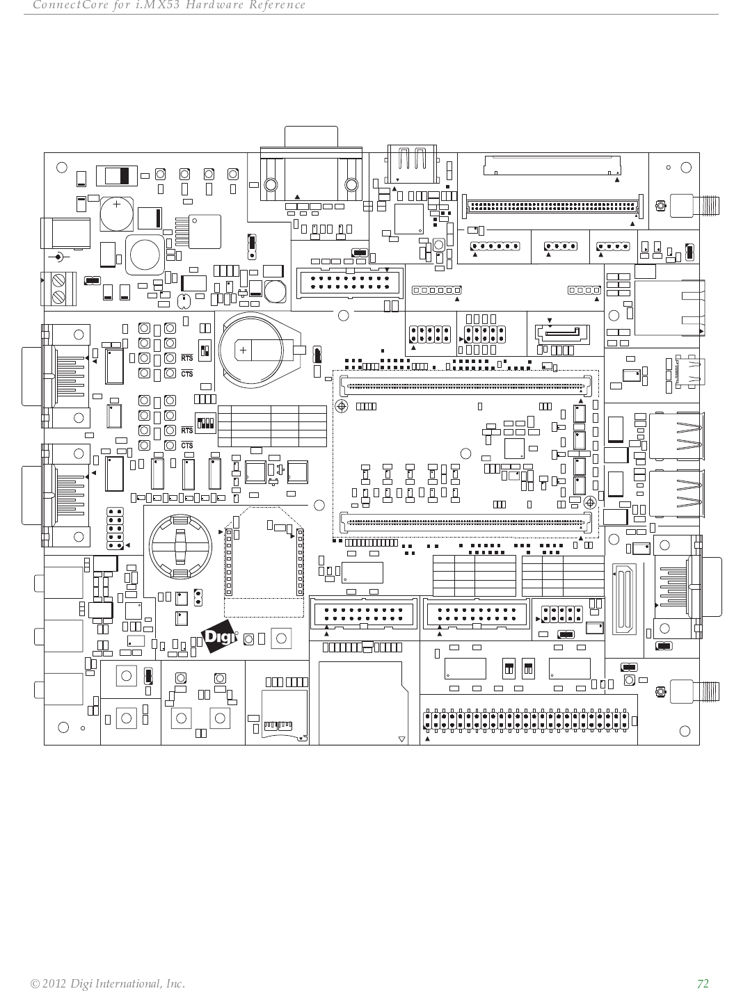
About the Development Board
The development board supports the ConnectCore for i.MX53 module. This chapter
describes the interfaces of the development board and explains how to configure the board
for your requirements.
The development board has two 180-pin connectors that mate with the module connectors.
What’s on the Development Board?
Flexible 9-30VDC charger power supply with power-on switch
Screw-flange Battery header with enable jumper
3V coin cell battery
+3.3V selection jumper. The +3.3V supply can be selected from the module or from
the development board.
Connectors for Digi 802.3af PoE Application board (sold separately)
1 x UART RS232 with status LEDs and SUB-D 9-pin connector
1 x UART MEI (RS232/RS4xx) with status LEDs and SUB-D 9-pin connector
1 x UART with TTL levels
1 x CAN bus with termination resistor selection and SUB-D 9-pin connector
1 x CAN bus with termination resistor selection and pin header
1 x USB OTG connector
4 x USB Host connectors
1 x SD/MMC card holder
1 x MicroSD card holder
1 x SATA connector
SPI and I2C headers
PWM header
Audio interface with Line-out, Line-In and Mic-In jacks
VGA interface

ȱ ȱ ȱ ȱ ȱ ȱ
ȱ ȱ ȱ ȱ ȱȱȱ
HDMI interface
Parallel LCD connector with Touch Screen interface
LVDS LCD connector with Touch Screen interface
Touch Screen selection circuit
2 x Camera connectors
RJ-45 Ethernet connector
Connector for a Digi 100M_ETHADPT (sold separately)
2 x RP-SMA WLAN antenna connectors
Digital I/O header
XBee socket with Association LED and Ident Button (XBee module sold separately)
1-Wire interface with 2-pin header
1-Wire EEPROM
1-Wire iButton retainer
Peripheral application header
Keypad header
JTAG interface
2 x User LEDs (green)
2 x User Push-buttons
Boot mode switch
Boot device switch
1 x Power Push-button
1 x Reset Push-button
ȱ ȱ ȱ ȱ ȱ ȱ
ȱ ȱ ȱ ȱ ȱȱȱ
The Development Board
R
U3
U50
ON
41 32
S6
ON
1 2
S7
ON
1 2
S8
ON
1 2
S9
S5
S3
S13
S10
H9
H3
D1
U21
U11
Q2
U8 U33
U32
X18
P24 P22 P23
P29
X24
J1
J2
P1
P21
X19
X21
X45 X20
J24
J13
J17
J6
J20
J7
J9
U13
U52 U53
U51 U54
U7
U55
U56
U29
U28
U61
U19
U24
U38
U43
U42
U41
U4
U20U22
U17
U36
U18
U26
U6
U2
U15
JP6
JP20
JP1
JP3
JP10
JP4
JP12
JP5
J19
X32
X29
X28
X7
P20
J11
P19
R139
J27
J10
J8
L8
L26
L27
L21
L19
L22
L20
L25
L24
L18
L28
L29
L9
L12
L16
L3
L4
D5
V5 V6
D6
P12
P13
S12
V2
X30
X27
X31
X14
X16 X15
X13
U46
U10
U35U31U14 U40
LE59LE62LE63 LE61 LE41
LE57
LE60
LE58
LE7 LE6LE4
LE8
LE51
LE49
LE40
LE43
LE42
LE44
LE47
LE48
LE45
LE46
LE12
LE50
J23
P14
P15
J15
J12
J18
V10
V11
O1 O2
R130
R131
R51
R133
R134
R28
R228
R56
R71
R75
R77
R74 R55R73
R59
R72
R57
R194
R96
R70
R18
R132
R14
R106
R108
R107
R105
R15
R11
+
C60
+
R52
R84
R41
C2
C1
P2
R45
R49
+
C3
+
R187
R189
R138
R159
R188
R5
R6
R7
C88
C87
C145
C86
R16
R42
R31
R39
R33
RN2
C85
R127
R8
R9
R36 R37
R34
R38
R35
R95
R89
R88
U37
U12
U16
U45
S2
C25
P4
C104
+
C49
C129
R53
C127
C48 C45
R182
C7 C6
L10
L6
L7
L5
R142
R86
+
C109
+
+
C108
+
+
C110
+
+
C111
+
C105
+
+
C90
+
R20
R181
R176
R12 R13
R85
R94
R195
R102
R101
C81
C103
C120
C169
C43
C53
C39
C27
C159
C161
C106
C46
C28
C162
C57
C155
R222
C163
C113 C114 C115
C126
C101
C125 C102
C69
C100
C95
C94
C59
C51
C56
C41
C26
C18
C50
C38
C83
C55
C58
C44
C89
C171
C78
C166
C165
C177
C84
C170
C52
C196
C118
C17
C123
C187
C98
C167
C117
C119
C79
C121
C188
C191
C179
R50
C99
C194
C97
C122
C189
C195
C158
C193
C186
C124
C96
C197
C80
C91
C93
C178
R199
C148
C147
C116
C107
C190
C192
C168
C112
R30
R17
R93
R27 R29
R135
R122
R10
U9
+
C20
+
R246
R247
C150
Y1
C153
C22
L23
R143
Y3
C151
C164
R23
C132
C134
C160
C131
C176
C175
C154
C174
C135
C133
C149
C70
C13
C12
C47
C61
C11
C71
C10
C62
C66
R118
R172
R4
R123
R61
R62
R63
R90
C23
R48
R117
R64
R76
R78
R141
R66
R79
R121
R65
R92
R91
R217
R21
R221
R100
R211
R110
R103
R99
R113
R2
R111
R126
R119
R25
R184
R104
R112
R1
R116
R220
R254
R154
R153
C157
C54
R137
L17
J5
U48
U47
U39
U34
U44
U25
U1 U23
U27
U5
R231
R204
R205
R218
R208
R289
R275
R274
R278
R287
R273
R261
R269
R206
R253
R202
R281
R203
R285
R290
R277
R284
R266
R257
R280
R282
R258
R259
R260
R276
R268
R22 R26
R19
R286
R283
R201
R262
R263
C128
R256
R265
R264
R207
R271
R158
R288
R272
R279
R291
R177
R213
R175
R179
R43
R178
R140
R209
R180
R232
R44
R47
R98
R58
R83
R24
R46
R270
R40
R174
R87
R109
R114
R3
R97
R129
R82
R124
R125
R152
R68
R151
R191
R227
R32
R193
R190
R196
R136
R230
R183
R192
R128
R120
R198
R229
R197
R162
C82
C37
C35
C15
C65 C67 C68
C36
C4
C5
C42
C29
C32
C34
C33
C64
C31
C156
C9
C63
C19
C30
C8
C14
C172
R81
R80
R186
R185
R67
R216
C152
C130
L11
L1
U57
LBL1
J4
R173
R214
C24
JP2
R292
C16
R69
R60
L30
R215
R171
U49
C21
U30
J3
C72
H1
R255
R293
U58
R54 C40
TP83TP85
TP61
TP90
TP114
TP67
TP66
TP115
TP69
TP116
TP71
TP117
TP74
TP78TP80
TP63
TP118
TP64
TP22
TP21
TP20
TP19
TP46
TP72
TP45
TP60
TP43
TP84
TP42
TP79
TP65
TP73
TP113
TP137
TP70
TP23
TP24TP81
TP47
TP48
TP77
TP76
TP75
TP93
TP38
TP49
TP52
TP51
TP39
TP41
TP25
TP82
TP89
TP87
TP62
TP29
TP30
TP31
TP28
TP91
TP33
TP35
TP57
TP26
TP37
TP88
TP86
TP68
TP58
TP36
TP92
TP27
TP44
X14
J17 P15
S8
CAN2
SATA
PWM
ON=
WLAN DISABLE
J19
J12
POWER
X27 ON=
P29
S9
S9
S5
_I2C
X21
CLOSE
RXD
J1
+3.3V_JS
SER DOWNLOAD
J18
+3.3V_MOD
DIGI
JTAG
S8
IDENT
DISABLED
USER
P22
+
LINE OUT
UART3 (TTL)
AUTO PWR DWN
J13
+
VCHRG
ON/CLOSE
P4
RESERVED
CAN1 TERMINATION
TXD
CLOSE
UART1 STATUS
X30
OPEN
P12
UART2 (MEI)
LE51
ETHERNET 1
SD/MMC
OPEN
X20
9V-30VDC
SPI
3
LE49
X15
RS485 MODE
+5V
DESCRIPTION
VBATT
J8
1
DISABLED
J10
MAIN POWER
OPEN
P24
J11
LE8
BOOT - SATA
ACTIVE
POS 1
OPEN
4
BUTTON 1
2-WIRE
S6
LVDS
LCD
OFF/OPEN
4-WIRE
ACTIVE
X32
POS
INT. BOOT
VGA
DESCRIPTION
2
MICRO SD
X28
WLAN PRIMARY
J27
ON=ENABLE
COIN CELL
X45
MICRO
1-WIRE
J15
INTERNATIONAL
ETHERNET 2
LE50
CAN1
WLAN SECONDARY
POS 2
J9
P1
OPEN
X29
J24
LED 2
LE4
X18
S13
PARALLEL LCD
S3
S12
XBEE MODULE
OFF
P2
J2
ON=AUTOBOOT
J20
i.MX53 MODULE
POS 1
J7
CLOSE OPEN
RXD
CLOSE
UART2 STATUS
BOOT - FUSES
X16
RESET
TERMINATION
P14
LINE IN
HDMI
X19
CLOSE
ASSOC
CLOSE CLOSE
BOOT - FLASH
POS 2
LED 1
CAN2 TERMINATION
S7
OPEN
X7
BOOT - uSD
BOOT - SD
J6
BUTTON 2
J23
P23
S2
LE6LE7
S10
KEYPAD
MODE
CAMERA 2
RS232
CONNECTCORE
RS422/485
EXT BATT
ENABLE EXT BATT
X24
TOUCH SELECTION
DESCRIPTION
ON
UART1 (CONSOLE)
+3.3VPOWER
LE12
CLOSE
DIGITAL I/O
TXD
PERIPHERAL CONNECTOR
CAMERA 1
BOOT CONF
USB OTG
USB HOST
ON=SJC-ONLY
AUDIO
J3
POE MODULE
P19
POE MODULE
BATT
OPEN
P20
P13
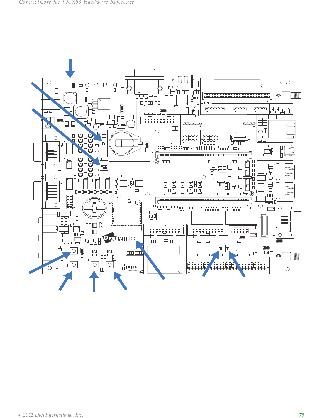
ȱ ȱ ȱ ȱ ȱ ȱ
ȱ ȱ ȱ ȱ ȱȱȱ
Switches and Push-buttons
Power Switch, S2
The development board has an ON/OFF switch, S2. The power switch S2 can switch both
9V-30VDC input power supply and 12VDC coming out of the optional PoE module
(Digi P/N DG-ACC-POE). However, if a power plug is present on the DC power jack, PoE is
disabled.
R
U3
U50
ON
41 32
S6
ON
1 2
S7
ON
1 2
S8
ON
1 2
S9
S5
S3
S13
S10
H9
H3
D1
U21
U11
Q2
U8 U33
U32
X18
P24 P22 P23
P29
X24
J1
J2
P1
P21
X19
X21
X45 X20
J24
J13
J17
J6
J20
J7
J9
U13
U52 U53
U51 U54
U7
U55
U56
U29
U28
U61
U19
U24
U38
U43
U42
U41
U4
U20U22
U17
U36
U18
U26
U6
U2
U15
JP6
JP20
JP1
JP3
JP10
JP4
JP12
JP5
J19
X32
X29
X28
X7
P20
J11
P19
R139
J27
J10
J8
L8
L26
L27
L21
L19
L22
L20
L25
L24
L18
L28
L29
L9
L12
L16
L3
L4
D5
V5 V6
D6
P12
P13
S12
V2
X30
X27
X31
X14
X16 X15
X13
U46
U10
U35U31U14 U40
LE59LE62LE63 LE61 LE41
LE57
LE60
LE58
LE7 LE6LE4LE8
LE51
LE49
LE40
LE43
LE42
LE44
LE47
LE48
LE45
LE46
LE12
LE50
J23
P14
P15
J15
J12
J18
V10
V11
O1 O2
R130
R131
R51
R133
R134
R28
R228
R56
R71
R75
R77
R74 R55R73
R59
R72
R57
R194
R96
R70
R18
R132
R14
R106
R108
R107
R105
R15
R11
+
C60
+
R52
R84
R41
C2
C1
P2
R45
R49
+
C3
+
R187
R189
R138
R159
R188
R5
R6
R7
C88
C87
C145
C86
R16
R42
R31
R39
R33
RN2
C85
R127
R8
R9
R36 R37
R34
R38
R35
R95
R89
R88
U37
U12
U16
U45
S2
C25
P4
C104
+
C49
C129
R53
C127
C48 C45
R182
C7 C6
L10
L6
L7
L5
R142
R86
+
C109
+
+
C108
+
+
C110
+
+
C111
+
C105
+
+
C90
+
R20
R181
R176
R12 R13
R85
R94
R195
R102
R101
C81
C103
C120
C169
C43
C53
C39
C27
C159
C161
C106
C46
C28
C162
C57
C155
R222
C163
C113 C114 C115
C126
C101
C125 C102
C69
C100
C95
C94
C59
C51
C56
C41
C26
C18
C50
C38
C83
C55
C58
C44
C89
C171
C78
C166
C165
C177
C84
C170
C52
C196
C118
C17
C123
C187
C98
C167
C117
C119
C79
C121
C188
C191
C179
R50
C99
C194
C97
C122
C189
C195
C158
C193
C186
C124
C96
C197
C80
C91
C93
C178
R199
C148
C147
C116
C107
C190
C192
C168
C112
R30
R17
R93
R27 R29
R135
R122
R10
U9
+
C20
+
R246
R247
C150
Y1
C153
C22
L23
R143
Y3
C151
C164
R23
C132
C134
C160
C131
C176
C175
C154
C174
C135
C133
C149
C70
C13
C12
C47
C61
C11
C71
C10
C62
C66
R118
R172
R4
R123
R61
R62
R63
R90
C23
R48
R117
R64
R76
R78
R141
R66
R79
R121
R65
R92
R91
R217
R21
R221
R100
R211
R110
R103
R99
R113
R2
R111
R126
R119
R25
R184
R104
R112
R1
R116
R220
R254
R154
R153
C157
C54
R137
L17
J5
U48
U47
U39
U34
U44
U25
U1 U23
U27
U5
R231
R204
R205
R218
R208
R289
R275
R274
R278
R287
R273
R261
R269
R206
R253
R202
R281
R203
R285
R290
R277
R284
R266
R257
R280
R282
R258
R259
R260
R276
R268
R22 R26
R19
R286
R283
R201
R262
R263
C128
R256
R265
R264
R207
R271
R158
R288
R272
R279
R291
R177
R213
R175
R179
R43
R178
R140
R209
R180
R232
R44
R47
R98
R58
R83
R24
R46
R270
R40
R174
R87
R109
R114
R3
R97
R129
R82
R124
R125
R152
R68
R151
R191
R227
R32
R193
R190
R196
R136
R230
R183
R192
R128
R120
R198
R229
R197
R162
C82
C37
C35
C15
C65 C67 C68
C36
C4
C5
C42
C29
C32
C34
C33
C64
C31
C156
C9
C63
C19
C30
C8
C14
C172
R81
R80
R186
R185
R67
R216
C152
C130
L11
L1
U57
LBL1
J4
R173
R214
C24
JP2
R292
C16
R69
R60
L30
R215
R171
U49
C21
U30
J3
C72
H1
R255
R293
U58
R54 C40
TP83TP85
TP61
TP90
TP114
TP67
TP66
TP115
TP69
TP116
TP71
TP117
TP74
TP78TP80
TP63
TP118
TP64
TP22
TP21
TP20
TP19
TP46
TP72
TP45
TP60
TP43
TP84
TP42
TP79
TP65
TP73
TP113
TP137
TP70
TP23
TP24TP81
TP47
TP48
TP77
TP76
TP75
TP93
TP38
TP49
TP52
TP51
TP39TP41
TP25
TP82
TP89
TP87
TP62
TP29
TP30
TP31
TP28
TP91
TP33
TP35
TP57
TP26
TP37
TP88
TP86
TP68
TP58
TP36
TP92
TP27
TP44
X14
J17 P15
S8
CAN2
SATA
PWM
ON=
WLAN DISABLE
J19
J12
POWER
X27
ON=
P29
S9
S9
S5
_I2C
X21
CLOSE
RXD
J1
+3.3V_JS
SER DOWNLOAD
J18
+3.3V_MOD
DIGI
JTAG
S8
IDENT
DISABLED
USER
P22
+
LINE OUT
UART3 (TTL)
AUTO PWR DWN
J13
+
VCHRG
ON/CLOSE
P4
RESERVED
CAN1 TERMINATION
TXD
CLOSE
UART1 STATUS
X30
OPEN
P12
UART2 (MEI)
LE51
ETHERNET 1
SD/MMC
OPEN
X20
9V-30VDC
SPI
3
LE49
X15
RS485 MODE
+5V
DESCRIPTION
VBATT
J8
1
DISABLED
J10
MAIN POWER
OPEN
P24
J11
LE8
BOOT - SATA
ACTIVE
POS 1
OPEN
4
BUTTON 1
2-WIRE
S6
LVDS
LCD
OFF/OPEN
4-WIRE
ACTIVE
X32
POS
INT. BOOT
VGA
DESCRIPTION
2
MICRO SD
X28
WLAN PRIMARY
J27
ON=ENABLE
COIN CELL
X45
MICRO
1-WIRE
J15
INTERNATIONAL
ETHERNET 2
LE50
CAN1
WLAN SECONDARY
POS 2
J9
P1
OPEN
X29
J24
LED 2
LE4
X18
S13
PARALLEL LCD
S3
S12
XBEE MODULE
OFF
P2
J2
ON=AUTOBOOT
J20
i.MX53 MODULE
POS 1
J7
CLOSE OPEN
RXD
CLOSE
UART2 STATUS
BOOT - FUSES
X16
RESET
TERMINATION
P14
LINE IN
HDMI
X19
CLOSE
ASSOC
CLOSE CLOSE
BOOT - FLASH
POS 2
LED 1
CAN2 TERMINATION
S7
OPEN
X7
BOOT - uSD
BOOT - SD
J6
BUTTON 2
J23
P23
S2
LE6LE7
S10
KEYPAD
MODE
CAMERA 2
RS232
CONNECTCORE
RS422/485
EXT BATT
ENABLE EXT BATT
X24
TOUCH SELECTION
DESCRIPTION
ON
UART1 (CONSOLE)
+3.3VPOWER
LE12
CLOSE
DIGITAL I/O
TXD
PERIPHERAL CONNECTOR
CAMERA 1
BOOT CONF
USB OTG
USB HOST
ON=SJC-ONLY
AUDIO
J3
POE MODULE
P19
POE MODULE
BATT
OPEN
P20
P13
Power Switch, S2
UART 1
Switch, S7
UART 2
Switch, S6
Power
Button, S13
Reset
Button,
S12
User
Button 1,
S3
User
Button 2,
S5
Ident
Button,
S10
Boot Device
Switch, S8
Boot Mode
Switch, S9
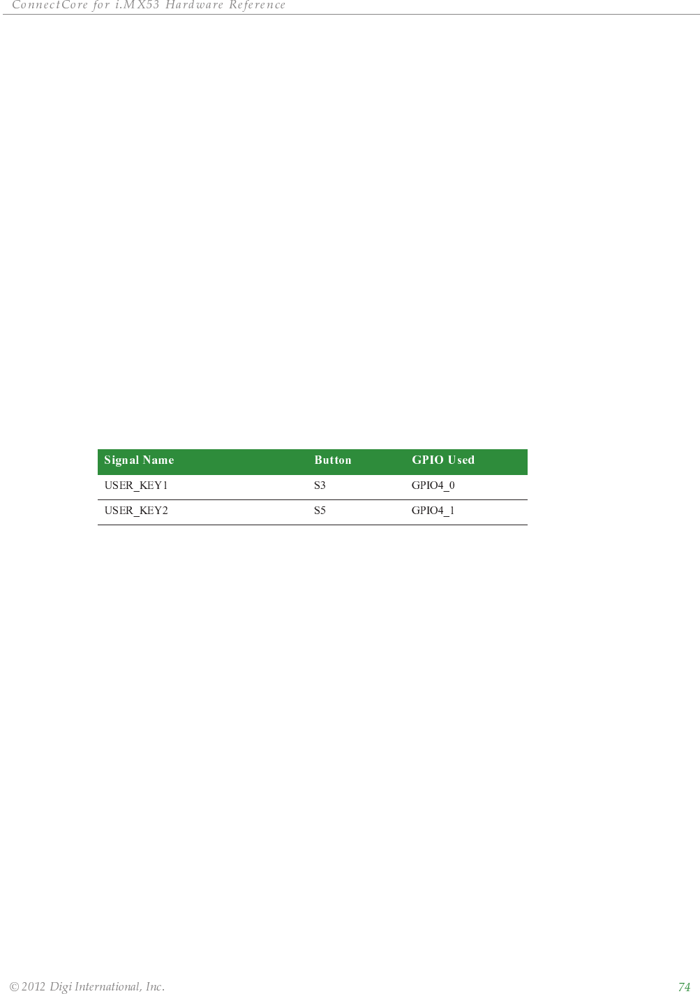
ȱ ȱ ȱ ȱ ȱ ȱ
ȱ ȱ ȱ ȱ ȱȱȱ
Reset Button, S12
The reset push-button S12, resets the module and the peripherals on the development board.
A push-button allows manual reset by connecting POR# or optionally RSTIN# to ground.
Power Button, S13
The power button S12 generates a power event for the i.MX53 and the DA9053 PMIC.
When the module is in Off mode, a Power event will power on the module.
When the module is in On mode, a long press (>2sec) of the power button will turn off the
module.
When the module is in On mode, a short press of the power button will put the module in
suspend mode (low power).
When the module is in Suspend mode, a short press of the power button will resume the
module.
User Buttons, S3 and S5
Use the user push-buttons to interact with the applications running on the ConnectCore for
i.MX53 module. Use these module signals to implement the push-buttons:
Ident Button, S10
The Ident push-button S10 is associated to the commissioning input of the Digi XBee modules.
This input provides a variety of simple functions to aid in deploying devices in a network. For
a deeply description of this functionality please refer to the Digi XBee modules
documentation.
Legend for Multi-Position Switches
Switches S6, S7, S8 and S9 are multi-pin switches. In the description tables for these
switches, the position is designated as S[switch number].[pin number]. For example, position
1 on switch S6 is specified as S6.1.
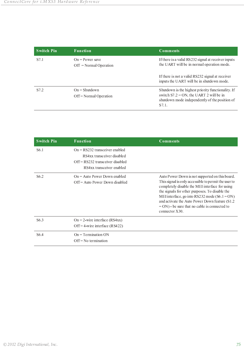
ȱ ȱ ȱ ȱ ȱ ȱ
ȱ ȱ ȱ ȱ ȱȱȱ
UART 1 Switch, S7
Use S7 to configure the line interface for serial port 1 (console):
UART 2 Switch, S6
Use S6 to configure the line interface for serial port 2 MEI:
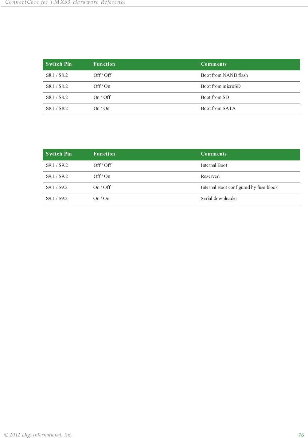
ȱ ȱ ȱ ȱ ȱ ȱ
ȱ ȱ ȱ ȱ ȱȱȱ
Boot Device Switch, S8
Use S8 to configure the source of the boot code when S9 is configured in internal boot mode.
Boot Mode Switch, S9
Use S9 to configure the module boot mode:
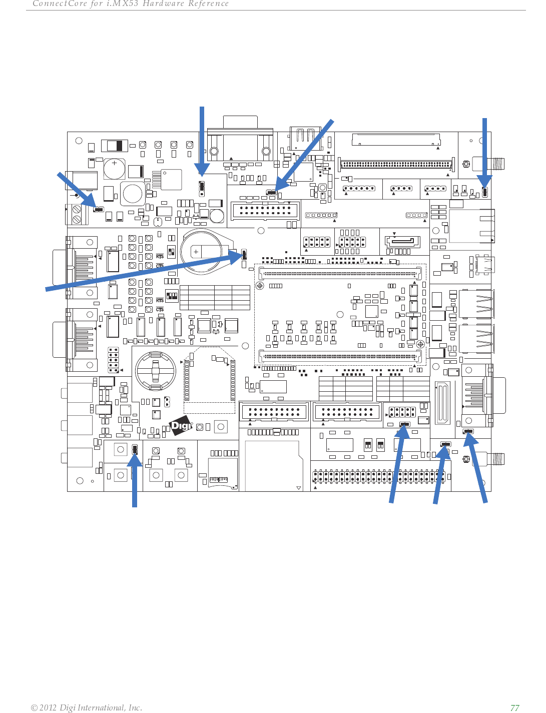
ȱ ȱ ȱ ȱ ȱ ȱ
ȱ ȱ ȱ ȱ ȱȱȱ
Jumpers
Battery Enable, J13
When J13 is set, the development board can be powered by an external battery connected to
J23.
+3.3V Source, P29
When set on positions 1-2, the +3.3V supply of the development board is generated in a
voltage regulator provided on the development board.
R
U3
U50
ON
41 32
S6
ON
1 2
S7
ON
1 2
S8
ON
1 2
S9
S5
S3
S13
S10
H9
H3
D1
U21
U11
Q2
U8 U33
U32
X18
P24 P22 P23
P29
X24
J1
J2
P1
P21
X19
X21
X45 X20
J24
J13
J17
J6
J20
J7
J9
U13
U52 U53
U51 U54
U7
U55
U56
U29
U28
U61
U19
U24
U38
U43
U42
U41
U4
U20U22
U17
U36
U18
U26
U6
U2
U15
JP6
JP20
JP1
JP3
JP10
JP4
JP12
JP5
J19
X32
X29
X28
X7
P20
J11
P19
R139
J27
J10
J8
L8
L26
L27
L21
L19
L22
L20
L25
L24
L18
L28
L29
L9
L12
L16
L3
L4
D5
V5 V6
D6
P12
P13
S12
V2
X30
X27
X31
X14
X16 X15
X13
U46
U10
U35U31U14 U40
LE59LE62LE63 LE61 LE41
LE57
LE60
LE58
LE7 LE6LE4
LE8
LE51
LE49
LE40
LE43
LE42
LE44
LE47
LE48
LE45
LE46
LE12
LE50
J23
P14
P15
J15
J12
J18
V10
V11
O1 O2
R130
R131
R51
R133
R134
R28
R228
R56
R71
R75
R77
R74 R55R73
R59
R72
R57
R194
R96
R70
R18
R132
R14
R106
R108
R107
R105
R15
R11
+
C60
+
R52
R84
R41
C2
C1
P2
R45
R49
+
C3
+
R187
R189
R138
R159
R188
R5
R6
R7
C88
C87
C145
C86
R16
R42
R31
R39
R33
RN2
C85
R127
R8
R9
R36 R37
R34
R38
R35
R95
R89
R88
U37
U12
U16
U45
S2
C25
P4
C104
+
C49
C129
R53
C127
C48 C45
R182
C7 C6
L10
L6
L7
L5
R142
R86
+
C109
+
+
C108
+
+
C110
+
+
C111
+
C105
+
+
C90
+
R20
R181
R176
R12 R13
R85
R94
R195
R102
R101
C81
C103
C120
C169
C43
C53
C39
C27
C159
C161
C106
C46
C28
C162
C57
C155
R222
C163
C113 C114 C115
C126
C101
C125 C102
C69
C100
C95
C94
C59
C51
C56
C41
C26
C18
C50
C38
C83
C55
C58
C44
C89
C171
C78
C166
C165
C177
C84
C170
C52
C196
C118
C17
C123
C187
C98
C167
C117
C119
C79
C121
C188
C191
C179
R50
C99
C194
C97
C122
C189
C195
C158
C193
C186
C124
C96
C197
C80
C91
C93
C178
R199
C148
C147
C116
C107
C190
C192
C168
C112
R30
R17
R93
R27 R29
R135
R122
R10
U9
+
C20
+
R246
R247
C150
Y1
C153
C22
L23
R143
Y3
C151
C164
R23
C132
C134
C160
C131
C176
C175
C154
C174
C135
C133
C149
C70
C13
C12
C47
C61
C11
C71
C10
C62
C66
R118
R172
R4
R123
R61
R62
R63
R90
C23
R48
R117
R64
R76
R78
R141
R66
R79
R121
R65
R92
R91
R217
R21
R221
R100
R211
R110
R103
R99
R113
R2
R111
R126
R119
R25
R184
R104
R112
R1
R116
R220
R254
R154
R153
C157
C54
R137
L17
J5
U48
U47
U39
U34
U44
U25
U1 U23
U27
U5
R231
R204
R205
R218
R208
R289
R275
R274
R278
R287
R273
R261
R269
R206
R253
R202
R281
R203
R285
R290
R277
R284
R266
R257
R280
R282
R258
R259
R260
R276
R268
R22 R26
R19
R286
R283
R201
R262
R263
C128
R256
R265
R264
R207
R271
R158
R288
R272
R279
R291
R177
R213
R175
R179
R43
R178
R140
R209
R180
R232
R44
R47
R98
R58
R83
R24
R46
R270
R40
R174
R87
R109
R114
R3
R97
R129
R82
R124
R125
R152
R68
R151
R191
R227
R32
R193
R190
R196
R136
R230
R183
R192
R128
R120
R198
R229
R197
R162
C82
C37
C35
C15
C65 C67 C68
C36
C4
C5
C42
C29
C32
C34
C33
C64
C31
C156
C9
C63
C19
C30
C8
C14
C172
R81
R80
R186
R185
R67
R216
C152
C130
L11
L1
U57
LBL1
J4
R173
R214
C24
JP2
R292
C16
R69
R60
L30
R215
R171
U49
C21
U30
J3
C72
H1
R255
R293
U58
R54 C40
TP83TP85
TP61
TP90
TP114
TP67
TP66
TP115
TP69
TP116
TP71
TP117
TP74
TP78TP80
TP63
TP118
TP64
TP22
TP21
TP20
TP19
TP46
TP72
TP45
TP60
TP43
TP84
TP42
TP79
TP65
TP73
TP113
TP137
TP70
TP23
TP24TP81
TP47
TP48
TP77
TP76
TP75
TP93
TP38
TP49
TP52
TP51
TP39TP41
TP25
TP82
TP89
TP87
TP62
TP29
TP30
TP31
TP28
TP91
TP33
TP35
TP57
TP26
TP37
TP88
TP86
TP68
TP58
TP36
TP92
TP27
TP44
X14
J17 P15
S8
CAN2
SATA
PWM
ON=
WLAN DISABLE
J19
J12
POWER
X27 ON=
P29
S9
S9
S5
_I2C
X21
CLOSE
RXD
J1
+3.3V_JS
SER DOWNLOAD
J18
+3.3V_MOD
DIGI
JTAG
S8
IDENT
DISABLED
USER
P22
+
LINE OUT
UART3 (TTL)
AUTO PWR DWN
J13
+
VCHRG
ON/CLOSE
P4
RESERVED
CAN1 TERMINATION
TXD
CLOSE
UART1 STATUS
X30
OPEN
P12
UART2 (MEI)
LE51
ETHERNET 1
SD/MMC
OPEN
X20
9V-30VDC
SPI
3
LE49
X15
RS485 MODE
+5V
DESCRIPTION
VBATT
J8
1
DISABLED
J10
MAIN POWER
OPEN
P24
J11
LE8
BOOT - SATA
ACTIVE
POS 1
OPEN
4
BUTTON 1
2-WIRE
S6
LVDS
LCD
OFF/OPEN
4-WIRE
ACTIVE
X32
POS
INT. BOOT
VGA
DESCRIPTION
2
MICRO SD
X28
WLAN PRIMARY
J27
ON=ENABLE
COIN CELL
X45
MICRO
1-WIRE
J15
INTERNATIONAL
ETHERNET 2
LE50
CAN1
WLAN SECONDARY
POS 2
J9
P1
OPEN
X29
J24
LED 2
LE4
X18
S13
PARALLEL LCD
S3
S12
XBEE MODULE
OFF
P2
J2
ON=AUTOBOOT
J20
i.MX53 MODULE
POS 1
J7
CLOSE OPEN
RXD
CLOSE
UART2 STATUS
BOOT - FUSES
X16
RESET
TERMINATION
P14
LINE IN
HDMI
X19
CLOSE
ASSOC
CLOSE CLOSE
BOOT - FLASH
POS 2
LED 1
CAN2 TERMINATION
S7
OPEN
X7
BOOT - uSD
BOOT - SD
J6
BUTTON 2
J23
P23
S2
LE6LE7
S10
KEYPAD
MODE
CAMERA 2
RS232
CONNECTCORE
RS422/485
EXT BATT
ENABLE EXT BATT
X24
TOUCH SELECTION
DESCRIPTION
ON
UART1 (CONSOLE)
+3.3VPOWER
LE12
CLOSE
DIGITAL I/O
TXD
PERIPHERAL CONNECTOR
CAMERA 1
BOOT CONF
USB OTG
USB HOST
ON=SJC-ONLY
AUDIO
J3
POE MODULE
P19
POE MODULE
BATT
OPEN
P20
P13
Battery
Enable,
J13
Autoboot, J6
Coincell
Enable,
J3
CAN2
Termination,
J9
CAN1
Termination,
J7
WLAN
Disable,
J17
Touch
Selection,
J20
JTAG Mod, J4
+3.3V Source, P29

ȱ ȱ ȱ ȱ ȱ ȱ
ȱ ȱ ȱ ȱ ȱȱȱ
When set on positions 2-3, the +3.3V supply of the development board is generated on the
module.
WLAN Disable, J17
When J17 is set, the WLAN interface is disabled.
Touch Selection, J20
When J20 is set, an external SPI touch screen controller is configured for the Parallel LCD
interface, and the internal analog touch screen controller (on module) is configured for the
LVDS interface.
When J20 is removed, an external SPI touch screen controller is configured for the LVDS
interface, and the internal analog touch screen controller (on module) is configured for the
parallel LCD interface.
Coincell Enable, J3
When J3 is set, +3V from the lithium coin cell battery is supplied to the RTC, even if the
board is switched off.
JTAG Mod, J4
When J4 is set, the Standard JTAG interface is the only debug capability enabled for the
ConnectCore for i.MX53.
When J4 is removed, the Trace port is also enabled for debugging.
Autoboot, J6
When J6 is set, the module boots as soon as the power supplies are present.
When J6 is removed, a power on event is needed to turn on the module.
CAN1 Termination resistor, J7
When J7 is set, a 120 Ohm termination resistor is connected to the CAN 1 lines.
CAN2 Termination resistor, J9
When J9 is set, a 120 Ohm termination resistor is connected to the CAN 2 lines.
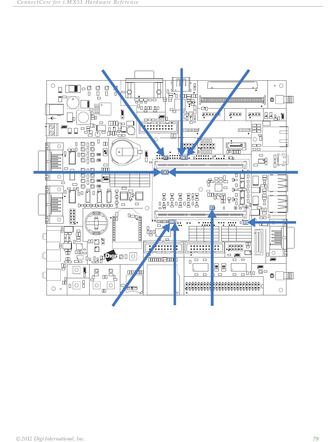
ȱ ȱ ȱ ȱ ȱ ȱ
ȱ ȱ ȱ ȱ ȱȱȱ
Configuration Resistors
R
U3
U50
ON
41 32
S6
ON
1 2
S7
ON
1 2
S8
ON
1 2
S9
S5
S3
S13
S10
H9
H3
D1
U21
U11
Q2
U8 U33
U32
X18
P24 P22 P23
P29
X24
J1
J2
P1
P21
X19
X21
X45 X20
J24
J13
J17
J6
J20
J7
J9
U13
U52 U53
U51 U54
U7
U55
U56
U29
U28
U61
U19
U24
U38
U43
U42
U41
U4
U20U22
U17
U36
U18
U26
U6
U2
U15
JP6
JP20
JP1
JP3
JP10
JP4
JP12
JP5
J19
X32
X29
X28
X7
P20
J11
P19
R139
J27
J10
J8
L8
L26
L27
L21
L19
L22
L20
L25
L24
L18
L28
L29
L9
L12
L16
L3
L4
D5
V5 V6
D6
P12
P13
S12
V2
X30
X27
X31
X14
X16 X15
X13
U46
U10
U35U31U14 U40
LE59LE62LE63 LE61 LE41
LE57
LE60
LE58
LE7 LE6LE4LE8
LE51
LE49
LE40
LE43
LE42
LE44
LE47
LE48
LE45
LE46
LE12
LE50
J23
P14
P15
J15
J12
J18
V10
V11
O1 O2
R130
R131
R51
R133
R134
R28
R228
R56
R71
R75
R77
R74 R55R73
R59
R72
R57
R194
R96
R70
R18
R132
R14
R106
R108
R107
R105
R15
R11
+
C60
+
R52
R84
R41
C2
C1
P2
R45
R49
+
C3
+
R187
R189
R138
R159
R188
R5
R6
R7
C88
C87
C145
C86
R16
R42
R31
R39
R33
RN2
C85
R127
R8
R9
R36 R37
R34
R38
R35
R95
R89
R88
U37
U12
U16
U45
S2
C25
P4
C104
+
C49
C129
R53
C127
C48 C45
R182
C7 C6
L10
L6
L7
L5
R142
R86
+
C109
+
+
C108
+
+
C110
+
+
C111
+
C105
+
+
C90
+
R20
R181
R176
R12 R13
R85
R94
R195
R102
R101
C81
C103
C120
C169
C43
C53
C39
C27
C159
C161
C106
C46
C28
C162
C57
C155
R222
C163
C113 C114 C115
C126
C101
C125 C102
C69
C100
C95
C94
C59
C51
C56
C41
C26
C18
C50
C38
C83
C55
C58
C44
C89
C171
C78
C166
C165
C177
C84
C170
C52
C196
C118
C17
C123
C187
C98
C167
C117
C119
C79
C121
C188
C191
C179
R50
C99
C194
C97
C122
C189
C195
C158
C193
C186
C124
C96
C197
C80
C91
C93
C178
R199
C148
C147
C116
C107
C190
C192
C168
C112
R30
R17
R93
R27 R29
R135
R122
R10
U9
+
C20
+
R246
R247
C150
Y1
C153
C22
L23
R143
Y3
C151
C164
R23
C132
C134
C160
C131
C176
C175
C154
C174
C135
C133
C149
C70
C13
C12
C47
C61
C11
C71
C10
C62
C66
R118
R172
R4
R123
R61
R62
R63
R90
C23
R48
R117
R64
R76
R78
R141
R66
R79
R121
R65
R92
R91
R217
R21
R221
R100
R211
R110
R103
R99
R113
R2
R111
R126
R119
R25
R184
R104
R112
R1
R116
R220
R254
R154
R153
C157
C54
R137
L17
J5
U48
U47
U39
U34
U44
U25
U1 U23
U27
U5
R231
R204
R205
R218
R208
R289
R275
R274
R278
R287
R273
R261
R269
R206
R253
R202
R281
R203
R285
R290
R277
R284
R266
R257
R280
R282
R258
R259
R260
R276
R268
R22 R26
R19
R286
R283
R201
R262
R263
C128
R256
R265
R264
R207
R271
R158
R288
R272
R279
R291
R177
R213
R175
R179
R43
R178
R140
R209
R180
R232
R44
R47
R98
R58
R83
R24
R46
R270
R40
R174
R87
R109
R114
R3
R97
R129
R82
R124
R125
R152
R68
R151
R191
R227
R32
R193
R190
R196
R136
R230
R183
R192
R128
R120
R198
R229
R197
R162
C82
C37
C35
C15
C65 C67 C68
C36
C4
C5
C42
C29
C32
C34
C33
C64
C31
C156
C9
C63
C19
C30
C8
C14
C172
R81
R80
R186
R185
R67
R216
C152
C130
L11
L1
U57
LBL1
J4
R173
R214
C24
JP2
R292
C16
R69
R60
L30
R215
R171
U49
C21
U30
J3
C72
H1
R255
R293
U58
R54 C40
TP83TP85
TP61
TP90
TP114
TP67
TP66
TP115
TP69
TP116
TP71
TP117
TP74
TP78TP80
TP63
TP118
TP64
TP22
TP21
TP20
TP19
TP46
TP72
TP45
TP60
TP43
TP84
TP42
TP79
TP65
TP73
TP113
TP137
TP70
TP23
TP24TP81
TP47
TP48
TP77
TP76
TP75
TP93
TP38
TP49
TP52
TP51
TP39
TP41
TP25
TP82
TP89
TP87
TP62
TP29
TP30
TP31
TP28
TP91
TP33
TP35
TP57
TP26
TP37
TP88
TP86
TP68
TP58
TP36
TP92
TP27
TP44
X14
J17 P15
S8
CAN2
SATA
PWM
ON=
WLAN DISABLE
J19
J12
POWER
X27
ON=
P29
S9
S9
S5
_I2C
X21
CLOSE
RXD
J1
+3.3V_JS
SER DOWNLOAD
J18
+3.3V_MOD
DIGI
JTAG
S8
IDENT
DISABLED
USER
P22
+
LINE OUT
UART3 (TTL)
AUTO PWR DWN
J13
+
VCHRG
ON/CLOSE
P4
RESERVED
CAN1 TERMINATION
TXD
CLOSE
UART1 STATUS
X30
OPEN
P12
UART2 (MEI)
LE51
ETHERNET 1
SD/MMC
OPEN
X20
9V-30VDC
SPI
3
LE49
X15
RS485 MODE
+5V
DESCRIPTION
VBATT
J8
1
DISABLED
J10
MAIN POWER
OPEN
P24
J11
LE8
BOOT - SATA
ACTIVE
POS 1
OPEN
4
BUTTON 1
2-WIRE
S6
LVDS
LCD
OFF/OPEN
4-WIRE
ACTIVE
X32
POS
INT. BOOT
VGA
DESCRIPTION
2
MICRO SD
X28
WLAN PRIMARY
J27
ON=ENABLE
COIN CELL
X45
MICRO
1-WIRE
J15
INTERNATIONAL
ETHERNET 2
LE50
CAN1
WLAN SECONDARY
POS 2
J9
P1
OPEN
X29
J24
LED 2
LE4
X18
S13
PARALLEL LCD
S3
S12
XBEE MODULE
OFF
P2
J2
ON=AUTOBOOT
J20
i.MX53 MODULE
POS 1
J7
CLOSE OPEN
RXD
CLOSE
UART2 STATUS
BOOT - FUSES
X16
RESET
TERMINATION
P14
LINE IN
HDMI
X19
CLOSE
ASSOC
CLOSE CLOSE
BOOT - FLASH
POS 2
LED 1
CAN2 TERMINATION
S7
OPEN
X7
BOOT - uSD
BOOT - SD
J6
BUTTON 2
J23
P23
S2
LE6LE7
S10
KEYPAD
MODE
CAMERA 2
RS232
CONNECTCORE
RS422/485
EXT BATT
ENABLE EXT BATT
X24
TOUCH SELECTION
DESCRIPTION
ON
UART1 (CONSOLE)
+3.3VPOWER
LE12
CLOSE
DIGITAL I/O
TXD
PERIPHERAL CONNECTOR
CAMERA 1
BOOT CONF
USB OTG
USB HOST
ON=SJC-ONLY
AUDIO
J3
POE MODULE
P19
POE MODULE
BATT
OPEN
P20
P13
DIGIO2
XBEE_ON_SLEEP#
DIGIO1
XBEE_SLEEP_RQ
CSI1_HSYNC
DISP1_HSYNC
UART1_RTS
SD3_CLK
UART1_CTS
SD3_CMD
DIGIO0
XBEE_RESET#
KEY_ROW7
CSI0_RESET#
KEY_COL7
CSI1_RESET#
CSI1_VSYNC
DISP1_VSYNC
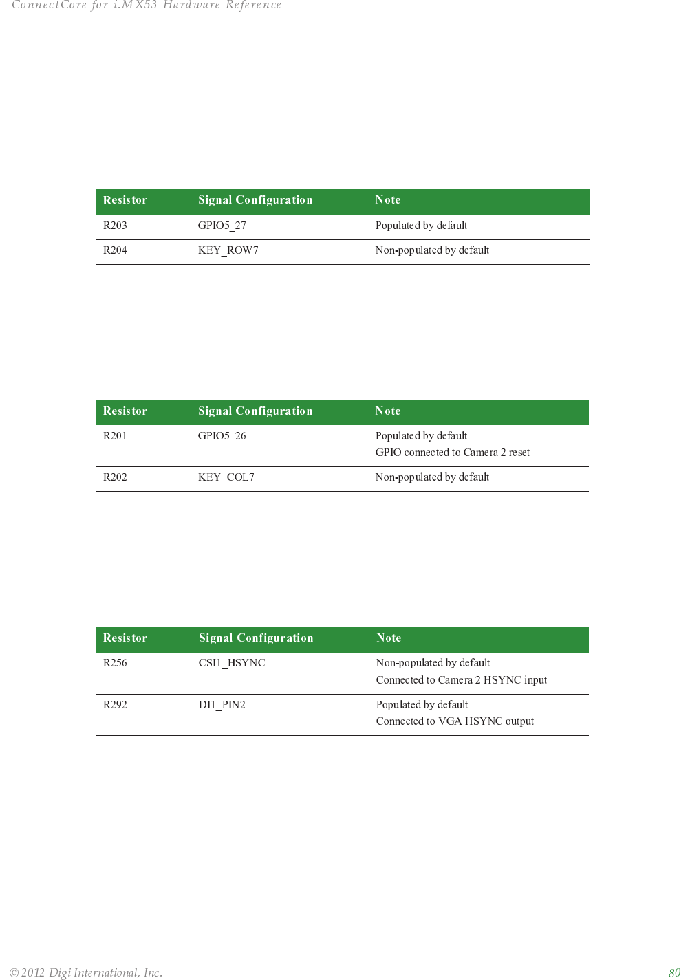
ȱ ȱ ȱ ȱ ȱ ȱ
ȱ ȱ ȱ ȱ ȱȱȱ
CSI0_RESET#/KEY_ROW7, R203/R204
The development board provides two 0 resistors, R203 and R204 to select the interface
where the KEY_ROW7/GPIO5_27 signal is connected. These two resistors should not be
populated at the same time.
The following table shows the configuration of these two resistors:
CSI1_RESET#/KEY_COL7, R201/R202
The development board provides two 0 resistors, R201 and R202 to select the interface
where the KEY_COL7/GPIO5_26 signal is connected. These two resistors should not be
populated at the same time.
The following table shows the configuration of these two resistors:
CSI1_HSYNC#/DISP1_HSYNC, R256/R292
The development board provides two 0 resistors, R256 and R292 to select the interface
where the EIM_DA11/CSI1_HSYNC signal is connected. These two resistors should not be
populated at the same time.
The following table shows the configuration of these two resistors:
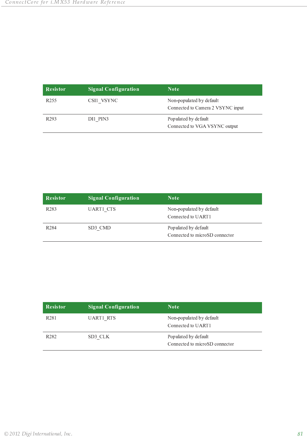
ȱ ȱ ȱ ȱ ȱ ȱ
ȱ ȱ ȱ ȱ ȱȱȱ
CSI1_VSYNC#/DISP1_VSYNC, R255/R293
The development board provides two 0 resistors, R255 and R293 to select the interface
where the EIM_DA12/CSI1_VSYNC signal is connected. These two resistors should not be
populated at the same time.
The following table shows the configuration of these two resistors:
UART1_CTS/SD3_CMD, R283/R284
The development board provides two 0 resistors, R283 and R284 to select the interface
where the SD3_CMD/UART1_CTS signal is connected. These two resistors should not be
populated at the same time.
The following table shows the configuration of these two resistors:
UART1_RTS/SD3_CLK, R281/R282
The development board provides two 0 resistors, R281 and R282 to select the interface
where the SD3_CLK/UART1_RTS signal is connected. These two resistors should not be
populated at the same time.
The following table shows the configuration of these two resistors:
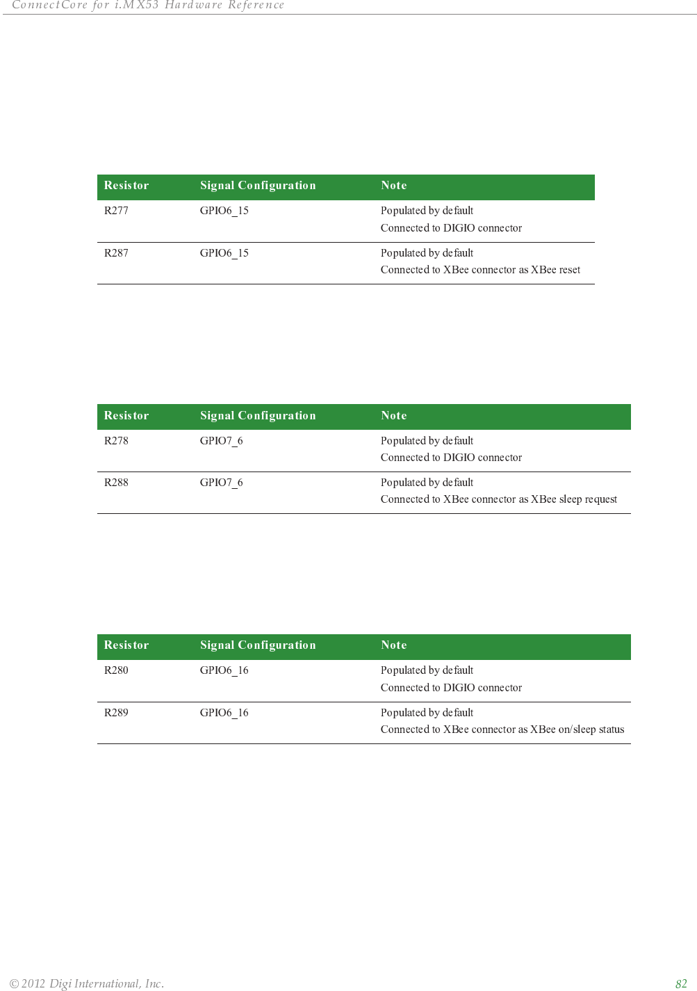
ȱ ȱ ȱ ȱ ȱ ȱ
ȱ ȱ ȱ ȱ ȱȱȱ
DIGIO0/XBEE_RESET#, R277/R287
The development board provides two 0 resistors, R277 and R287 to select the interface
where the GPIO6_15 signal is connected.
The following table shows the configuration of these two resistors:
DIGIO1/XBEE_SLEEP_RQ, R278/R288
The development board provides two 0 resistors, R278 and R288 to select the interface
where the GPIO7_6 signal is connected.
The following table shows the configuration of these two resistors:
DIGIO2/XBEE_ON_SLEEP#, R280/R289
The development board provides two 0 resistors, R280 and R289 to select the interface
where the GPIO6_16 signal is connected.
The following table shows the configuration of these two resistors:
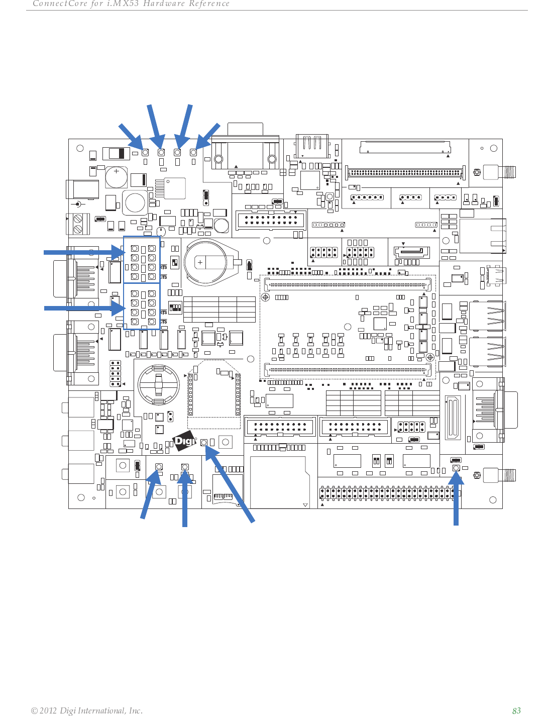
ȱ ȱ ȱ ȱ ȱ ȱ
ȱ ȱ ȱ ȱ ȱȱȱ
LEDs
WLAN, LE12
Green LED indicating WLAN operational status.
R
U3
U50
ON
41 32
S6
ON
1 2
S7
ON
1 2
S8
ON
1 2
S9
S5
S3
S13
S10
H9
H3
D1
U21
U11
Q2
U8 U33
U32
X18
P24 P22 P23
P29
X24
J1
J2
P1
P21
X19
X21
X45 X20
J24
J13
J17
J6
J20
J7
J9
U13
U52 U53
U51 U54
U7
U55
U56
U29
U28
U61
U19
U24
U38
U43
U42
U41
U4
U20U22
U17
U36
U18
U26
U6
U2
U15
JP6
JP20
JP1
JP3
JP10
JP4
JP12
JP5
J19
X32
X29
X28
X7
P20
J11
P19
R139
J27
J10
J8
L8
L26
L27
L21
L19
L22
L20
L25
L24
L18
L28
L29
L9
L12
L16
L3
L4
D5
V5 V6
D6
P12
P13
S12
V2
X30
X27
X31
X14
X16 X15
X13
U46
U10
U35U31U14 U40
LE59LE62LE63 LE61 LE41
LE57
LE60
LE58
LE7 LE6LE4
LE8
LE51
LE49
LE40
LE43
LE42
LE44
LE47
LE48
LE45
LE46
LE12
LE50
J23
P14
P15
J15
J12
J18
V10
V11
O1 O2
R130
R131
R51
R133
R134
R28
R228
R56
R71
R75
R77
R74 R55R73
R59
R72
R57
R194
R96
R70
R18
R132
R14
R106
R108
R107
R105
R15
R11
+
C60
+
R52
R84
R41
C2
C1
P2
R45
R49
+
C3
+
R187
R189
R138
R159
R188
R5
R6
R7
C88
C87
C145
C86
R16
R42
R31
R39
R33
RN2
C85
R127
R8
R9
R36 R37
R34
R38
R35
R95
R89
R88
U37
U12
U16
U45
S2
C25
P4
C104
+
C49
C129
R53
C127
C48 C45
R182
C7 C6
L10
L6
L7
L5
R142
R86
+
C109
+
+
C108
+
+
C110
+
+
C111
+
C105
+
+
C90
+
R20
R181
R176
R12 R13
R85
R94
R195
R102
R101
C81
C103
C120
C169
C43
C53
C39
C27
C159
C161
C106
C46
C28
C162
C57
C155
R222
C163
C113 C114 C115
C126
C101
C125 C102
C69
C100
C95
C94
C59
C51
C56
C41
C26
C18
C50
C38
C83
C55
C58
C44
C89
C171
C78
C166
C165
C177
C84
C170
C52
C196
C118
C17
C123
C187
C98
C167
C117
C119
C79
C121
C188
C191
C179
R50
C99
C194
C97
C122
C189
C195
C158
C193
C186
C124
C96
C197
C80
C91
C93
C178
R199
C148
C147
C116
C107
C190
C192
C168
C112
R30
R17
R93
R27 R29
R135
R122
R10
U9
+
C20
+
R246
R247
C150
Y1
C153
C22
L23
R143
Y3
C151
C164
R23
C132
C134
C160
C131
C176
C175
C154
C174
C135
C133
C149
C70
C13
C12
C47
C61
C11
C71
C10
C62
C66
R118
R172
R4
R123
R61
R62
R63
R90
C23
R48
R117
R64
R76
R78
R141
R66
R79
R121
R65
R92
R91
R217
R21
R221
R100
R211
R110
R103
R99
R113
R2
R111
R126
R119
R25
R184
R104
R112
R1
R116
R220
R254
R154
R153
C157
C54
R137
L17
J5
U48
U47
U39
U34
U44
U25
U1 U23
U27
U5
R231
R204
R205
R218
R208
R289
R275
R274
R278
R287
R273
R261
R269
R206
R253
R202
R281
R203
R285
R290
R277
R284
R266
R257
R280
R282
R258
R259
R260
R276
R268
R22 R26
R19
R286
R283
R201
R262
R263
C128
R256
R265
R264
R207
R271
R158
R288
R272
R279
R291
R177
R213
R175
R179
R43
R178
R140
R209
R180
R232
R44
R47
R98
R58
R83
R24
R46
R270
R40
R174
R87
R109
R114
R3
R97
R129
R82
R124
R125
R152
R68
R151
R191
R227
R32
R193
R190
R196
R136
R230
R183
R192
R128
R120
R198
R229
R197
R162
C82
C37
C35
C15
C65 C67 C68
C36
C4
C5
C42
C29
C32
C34
C33
C64
C31
C156
C9
C63
C19
C30
C8
C14
C172
R81
R80
R186
R185
R67
R216
C152
C130
L11
L1
U57
LBL1
J4
R173
R214
C24
JP2
R292
C16
R69
R60
L30
R215
R171
U49
C21
U30
J3
C72
H1
R255
R293
U58
R54 C40
TP83TP85
TP61
TP90
TP114
TP67
TP66
TP115
TP69
TP116
TP71
TP117
TP74
TP78TP80
TP63
TP118
TP64
TP22
TP21
TP20
TP19
TP46
TP72
TP45
TP60
TP43
TP84
TP42
TP79
TP65
TP73
TP113
TP137
TP70
TP23
TP24TP81
TP47
TP48
TP77
TP76
TP75
TP93
TP38
TP49
TP52
TP51
TP39
TP41
TP25
TP82
TP89
TP87
TP62
TP29
TP30
TP31
TP28
TP91
TP33
TP35
TP57
TP26
TP37
TP88
TP86
TP68
TP58
TP36
TP92
TP27
TP44
X14
J17 P15
S8
CAN2
SATA
PWM
ON=
WLAN DISABLE
J19
J12
POWER
X27 ON=
P29
S9
S9
S5
_I2C
X21
CLOSE
RXD
J1
+3.3V_JS
SER DOWNLOAD
J18
+3.3V_MOD
DIGI
JTAG
S8
IDENT
DISABLED
USER
P22
+
LINE OUT
UART3 (TTL)
AUTO PWR DWN
J13
+
VCHRG
ON/CLOSE
P4
RESERVED
CAN1 TERMINATION
TXD
CLOSE
UART1 STATUS
X30
OPEN
P12
UART2 (MEI)
LE51
ETHERNET 1
SD/MMC
OPEN
X20
9V-30VDC
SPI
3
LE49
X15
RS485 MODE
+5V
DESCRIPTION
VBATT
J8
1
DISABLED
J10
MAIN POWER
OPEN
P24
J11
LE8
BOOT - SATA
ACTIVE
POS 1
OPEN
4
BUTTON 1
2-WIRE
S6
LVDS
LCD
OFF/OPEN
4-WIRE
ACTIVE
X32
POS
INT. BOOT
VGA
DESCRIPTION
2
MICRO SD
X28
WLAN PRIMARY
J27
ON=ENABLE
COIN CELL
X45
MICRO
1-WIRE
J15
INTERNATIONAL
ETHERNET 2
LE50
CAN1
WLAN SECONDARY
POS 2
J9
P1
OPEN
X29
J24
LED 2
LE4
X18
S13
PARALLEL LCD
S3
S12
XBEE MODULE
OFF
P2
J2
ON=AUTOBOOT
J20
i.MX53 MODULE
POS 1
J7
CLOSE OPEN
RXD
CLOSE
UART2 STATUS
BOOT - FUSES
X16
RESET
TERMINATION
P14
LINE IN
HDMI
X19
CLOSE
ASSOC
CLOSE CLOSE
BOOT - FLASH
POS 2
LED 1
CAN2 TERMINATION
S7
OPEN
X7
BOOT - uSD
BOOT - SD
J6
BUTTON 2
J23
P23
S2
LE6LE7
S10
KEYPAD
MODE
CAMERA 2
RS232
CONNECTCORE
RS422/485
EXT BATT
ENABLE EXT BATT
X24
TOUCH SELECTION
DESCRIPTION
ON
UART1 (CONSOLE)
+3.3VPOWER
LE12
CLOSE
DIGITAL I/O
TXD
PERIPHERAL CONNECTOR
CAMERA 1
BOOT CONF
USB OTG
USB HOST
ON=SJC-ONLY
AUDIO
J3
POE MODULE
P19
POE MODULE
BATT
OPEN
P20
P13
WLAN, LE12
UART 1
Status
LEDs
USER LED1,
LE51
Assoc.,
LED50
USER LED2,
LE49
Charger,
LE8
UART 2
Status
LEDs
Battery,
LE4
+3.3V,
LE7 +5V,
LE6
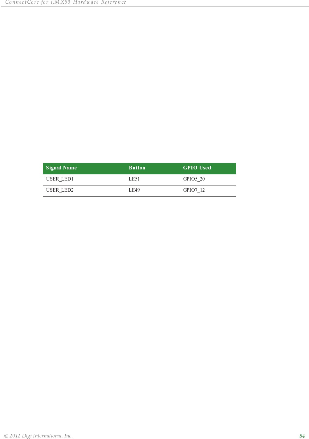
ȱ ȱ ȱ ȱ ȱ ȱ
ȱ ȱ ȱ ȱ ȱȱȱ
Power LEDs LE4, LE6, LE7 and LE8
The power LEDs show the status of their power supplies. All power LEDs are red.
LE4 ON indicates that battery power is present or that the DA9053 PMIC is charging
the battery. The intensity of the LED will change depending on the battery voltage
and depending on the charging voltage.
LE6 ON indicates that +5VDC power for the development board is present
LE7 ON indicates that +3.3VDC power for the development board is present
LE8 ON indicates that charger power is present
User LEDs, LE49 and LE51
The user LEDs are controlled through applications running on the ConnectCore for i.MX53
module. You may use these module signals to implement the LEDs:
Serial Status LEDs
The development board has two sets of serial port LEDs - four for serial port 1 and four for
serial port 2. The LEDs are connected to the TTL side of the RS232 or RS4xx transceivers.
Green means corresponding signal high
Red means corresponding signal low
The intensity and color of the LED will change when the voltage is switching
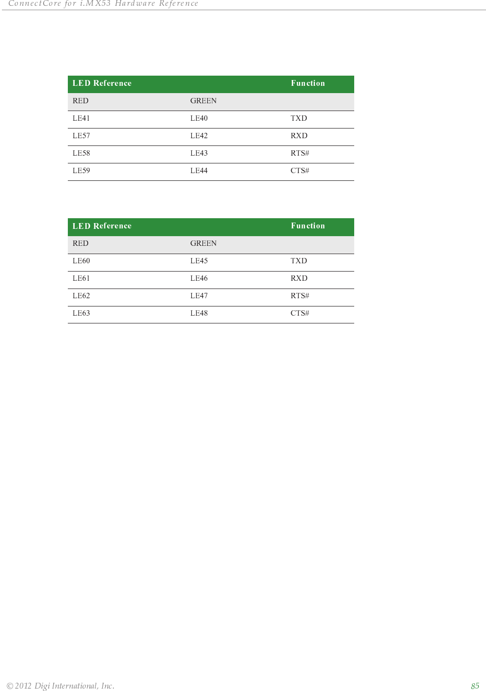
ȱ ȱ ȱ ȱ ȱ ȱ
ȱ ȱ ȱ ȱ ȱȱȱ
UART 1 Status LEDs
UART 2 Status LEDs
XBee Assoc., LE50
This LED is connected to the Associate output of the Digi XBee module. This LED provides
information of the device's network status and diagnostics information. For a more in-depth
description of this LED please refer to the Digi XBee module documentation available on the
Digi website.
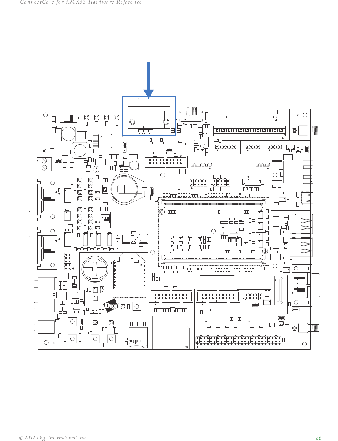
ȱ ȱ ȱ ȱ ȱ ȱ
ȱ ȱ ȱ ȱ ȱȱȱ
Analog Video Interface (VGA)
Analog Video Connector, X32
connector. The Analog Video interface is connected to the television encoder interface (TVE)
and to the display 2 synchronization interface (DISP1) of the i.MX53 CPU.
R
U3
U50
ON
41 32
S6
ON
1 2
S7
ON
1 2
S8
ON
1 2
S9
S5
S3
S13
S10
H9
H3
D1
U21
U11
Q2
U8 U33
U32
X18
P24 P22 P23
P29
X24
J1
J2
P1
P21
X19
X21
X45 X20
J24
J13
J17
J6
J20
J7
J9
U13
U52 U53
U51 U54
U7
U55
U56
U29
U28
U61
U19
U24
U38
U43
U42
U41
U4
U20U22
U17
U36
U18
U26
U6
U2
U15
JP6
JP20
JP1
JP3
JP10
JP4
JP12
JP5
J19
X32
X29
X28
X7
P20
J11
P19
R139
J27
J10
J8
L8
L26
L27
L21
L19
L22
L20
L25
L24
L18
L28
L29
L9
L12
L16
L3
L4
D5
V5 V6
D6
P12
P13
S12
V2
X30
X27
X31
X14
X16 X15
X13
U46
U10
U35U31U14 U40
LE59LE62LE63 LE61 LE41
LE57
LE60
LE58
LE7 LE6LE4
LE8
LE51
LE49
LE40
LE43
LE42
LE44
LE47
LE48
LE45
LE46
LE12
LE50
J23
P14
P15
J15
J12
J18
V10
V11
O1 O2
R130
R131
R51
R133
R134
R28
R228
R56
R71
R75
R77
R74 R55R73
R59
R72
R57
R194
R96
R70
R18
R132
R14
R106
R108
R107
R105
R15
R11
+
C60
+
R52
R84
R41
C2
C1
P2
R45
R49
+
C3
+
R187
R189
R138
R159
R188
R5
R6
R7
C88
C87
C145
C86
R16
R42
R31
R39
R33
RN2
C85
R127
R8
R9
R36 R37
R34
R38
R35
R95
R89
R88
U37
U12
U16
U45
S2
C25
P4
C104
+
C49
C129
R53
C127
C48 C45
R182
C7 C6
L10
L6
L7
L5
R142
R86
+
C109
+
+
C108
+
+
C110
+
+
C111
+
C105
+
+
C90
+
R20
R181
R176
R12 R13
R85
R94
R195
R102
R101
C81
C103
C120
C169
C43
C53
C39
C27
C159
C161
C106
C46
C28
C162
C57
C155
R222
C163
C113 C114 C115
C126
C101
C125 C102
C69
C100
C95
C94
C59
C51
C56
C41
C26
C18
C50
C38
C83
C55
C58
C44
C89
C171
C78
C166
C165
C177
C84
C170
C52
C196
C118
C17
C123
C187
C98
C167
C117
C119
C79
C121
C188C191
C179
R50
C99
C194
C97
C122
C189
C195
C158
C193
C186
C124
C96
C197
C80
C91
C93
C178
R199
C148
C147
C116
C107
C190
C192
C168
C112
R30
R17
R93
R27 R29
R135
R122
R10
U9
+
C20
+
R246
R247
C150
Y1
C153
C22
L23
R143
Y3
C151
C164
R23
C132
C134
C160
C131
C176
C175
C154
C174
C135
C133
C149
C70
C13
C12
C47
C61
C11
C71
C10
C62
C66
R118
R172
R4
R123
R61
R62
R63
R90
C23
R48
R117
R64
R76
R78
R141
R66
R79
R121
R65
R92
R91
R217
R21
R221
R100
R211
R110
R103
R99
R113
R2
R111
R126
R119
R25
R184
R104
R112
R1
R116
R220
R254
R154
R153
C157
C54
R137
L17
J5
U48
U47
U39
U34
U44
U25
U1 U23
U27
U5
R231
R204
R205
R218
R208
R289
R275
R274
R278
R287
R273
R261
R269
R206
R253
R202
R281
R203
R285
R290
R277
R284
R266
R257
R280
R282
R258
R259
R260
R276
R268
R22 R26
R19
R286
R283
R201
R262
R263
C128
R256
R265
R264
R207
R271
R158
R288
R272
R279
R291
R177
R213
R175
R179
R43
R178
R140
R209
R180
R232
R44
R47
R98
R58
R83
R24
R46
R270
R40
R174
R87
R109
R114
R3
R97
R129
R82
R124
R125
R152
R68
R151
R191
R227
R32
R193
R190
R196
R136
R230
R183
R192
R128
R120
R198
R229
R197
R162
C82
C37
C35
C15
C65 C67 C68
C36
C4
C5
C42
C29
C32
C34
C33
C64
C31
C156
C9
C63
C19
C30
C8
C14
C172
R81
R80
R186
R185
R67
R216
C152
C130
L11
L1
U57
LBL1
J4
R173
R214
C24
JP2
R292
C16
R69
R60
L30
R215
R171
U49
C21
U30
J3
C72
H1
R255
R293
U58
R54 C40
TP83TP85
TP61
TP90
TP114
TP67
TP66
TP115
TP69
TP116
TP71
TP117
TP74
TP78TP80
TP63
TP118
TP64
TP22
TP21
TP20
TP19
TP46
TP72
TP45
TP60
TP43
TP84
TP42
TP79
TP65
TP73
TP113
TP137
TP70
TP23
TP24TP81
TP47
TP48
TP77
TP76
TP75
TP93
TP38
TP49
TP52
TP51
TP39
TP41
TP25
TP82
TP89
TP87
TP62
TP29
TP30
TP31
TP28
TP91
TP33
TP35
TP57
TP26
TP37
TP88
TP86
TP68
TP58
TP36
TP92
TP27
TP44
X14
J17 P15
S8
CAN2
SATA
PWM
ON=
WLAN DISABLE
J19
J12
POWER
X27
ON=
P29
S9
S9
S5
_I2C
X21
CLOSE
RXD
J1
+3.3V_JS
SER DOWNLOAD
J18
+3.3V_MOD
DIGI
JTAG
S8
IDENT
DISABLED
USER
P22
+
LINE OUT
UART3 (TTL)
AUTO PWR DWN
J13
+
VCHRG
ON/CLOSE
P4
RESERVED
CAN1 TERMINATION
TXD
CLOSE
UART1 STATUS
X30
OPEN
P12
UART2 (MEI)
LE51
ETHERNET 1
SD/MMC
OPEN
X20
9V-30VDC
SPI
3
LE49
X15
RS485 MODE
+5V
DESCRIPTION
VBATT
J8
1
DISABLED
J10
MAIN POWER
OPEN
P24
J11
LE8
BOOT - SATA
ACTIVE
POS 1
OPEN
4
BUTTON 1
2-WIRE
S6
LVDS
LCD
OFF/OPEN
4-WIRE
ACTIVE
X32
POS
INT. BOOT
VGA
DESCRIPTION
2
MICRO SD
X28
WLAN PRIMARY
J27
ON=ENABLE
COIN CELL
X45
MICRO
1-WIRE
J15
INTERNATIONAL
ETHERNET 2
LE50
CAN1
WLAN SECONDARY
POS 2
J9
P1
OPEN
X29
J24
LED 2
LE4
X18
S13
PARALLEL LCD
S3
S12
XBEE MODULE
OFF
P2
J2
ON=AUTOBOOT
J20
i.MX53 MODULE
POS 1
J7
CLOSE OPEN
RXD
CLOSE
UART2 STATUS
BOOT - FUSES
X16
RESET
TERMINATION
P14
LINE IN
HDMI
X19
CLOSE
ASSOC
CLOSE CLOSE
BOOT - FLASH
POS 2
LED 1
CAN2 TERMINATION
S7
OPEN
X7
BOOT - uSD
BOOT - SD
J6
BUTTON 2
J23
P23
S2
LE6LE7
S10
KEYPAD
MODE
CAMERA 2
RS232
CONNECTCORE
RS422/485
EXT BATT
ENABLE EXT BATT
X24
TOUCH SELECTION
DESCRIPTION
ON
UART1 (CONSOLE)
+3.3VPOWER
LE12
CLOSE
DIGITAL I/O
TXD
PERIPHERAL CONNECTOR
CAMERA 1
BOOT CONF
USB OTG
USB HOST
ON=SJC-ONLY
AUDIO
J3
POE MODULE
P19
POE MODULE
BATT
OPEN
P20
P13
VGA Connector, X32
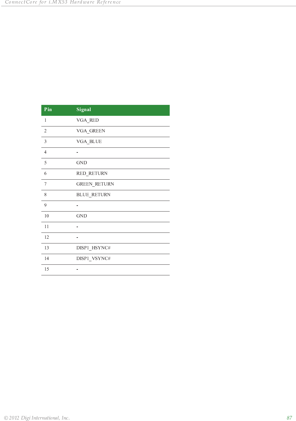
ȱ ȱ ȱ ȱ ȱ ȱ
ȱ ȱ ȱ ȱ ȱȱȱ
The VGA interface shares share the functionality in the development board with the
bootstrap interface and with the camera 2 interface. To avoid conflict between the camera
2/VGA signals and the bootstrap interface, a delay circuit is provided in the board to disable
the camera 2 and the VGA interfaces while the bootstrap configuration is being reading by
the i.MX53 CPU. Once the bootstrap configuration has been read the camera 2 and the VGA
interfaces are enabled. To avoid conflicts between the camera 2 and the VGA interface 0
resistors are used to select the interface to be used. Please refer to the "Configuration
Resistors" section on page 79 for detailed information.
The table below shows the pinout of the Analog Video connector.
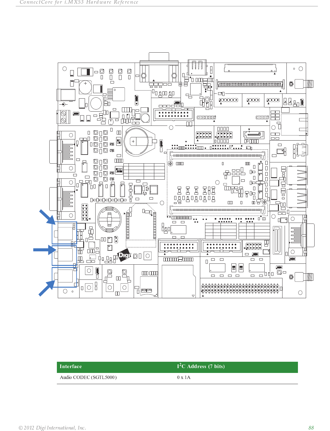
ȱ ȱ ȱ ȱ ȱ ȱ
ȱ ȱ ȱ ȱ ȱȱȱ
Audio Interface
The development board provides an audio interface with line in, line out, and microphone in.
The Freescale SGTL5000 audio CODEC on the development board is controlled through I2C
port 3 of the ConnectCore for i.MX53 module. Digital audio data is sent/receive between the
audio CODEC and the module through the I2S interface (AUD5 channel of the i.MX53
AUDMUX).
R
U3
U50
ON
41 32
S6
ON
1 2
S7
ON
1 2
S8
ON
1 2
S9
S5
S3
S13
S10
H9
H3
D1
U21
U11
Q2
U8 U33
U32
X18
P24 P22 P23
P29
X24
J1
J2
P1
P21
X19
X21
X45 X20
J24
J13
J17
J6
J20
J7
J9
U13
U52 U53
U51 U54
U7
U55
U56
U29
U28
U61
U19
U24
U38
U43
U42
U41
U4
U20U22
U17
U36
U18
U26
U6
U2
U15
JP6
JP20
JP1
JP3
JP10
JP4
JP12
JP5
J19
X32
X29
X28
X7
P20
J11
P19
R139
J27
J10
J8
L8
L26
L27
L21
L19
L22
L20
L25
L24
L18
L28
L29
L9
L12
L16
L3
L4
D5
V5 V6
D6
P12
P13
S12
V2
X30
X27
X31
X14
X16 X15
X13
U46
U10
U35U31U14 U40
LE59LE62LE63 LE61 LE41
LE57
LE60
LE58
LE7 LE6LE4
LE8
LE51
LE49
LE40
LE43
LE42
LE44
LE47
LE48
LE45
LE46
LE12
LE50
J23
P14
P15
J15
J12
J18
V10
V11
O1 O2
R130
R131
R51
R133
R134
R28
R228
R56
R71
R75
R77
R74 R55R73
R59
R72
R57
R194
R96
R70
R18
R132
R14
R106
R108
R107
R105
R15
R11
+
C60
+
R52
R84
R41
C2
C1
P2
R45
R49
+
C3
+
R187
R189
R138
R159
R188
R5
R6
R7
C88
C87
C145
C86
R16
R42
R31
R39
R33
RN2
C85
R127
R8
R9
R36 R37
R34
R38
R35
R95
R89
R88
U37
U12
U16
U45
S2
C25
P4
C104
+
C49
C129
R53
C127
C48 C45
R182
C7 C6
L10
L6
L7
L5
R142
R86
+
C109
+
+
C108
+
+
C110
+
+
C111
+
C105
+
+
C90
+
R20
R181
R176
R12 R13
R85
R94
R195
R102
R101
C81
C103
C120
C169
C43
C53
C39
C27
C159
C161
C106
C46
C28
C162
C57
C155
R222
C163
C113 C114 C115
C126
C101
C125 C102
C69
C100
C95
C94
C59
C51
C56
C41
C26
C18
C50
C38
C83
C55
C58
C44
C89
C171
C78
C166
C165
C177
C84
C170
C52
C196
C118
C17
C123
C187
C98
C167
C117
C119
C79
C121
C188
C191
C179
R50
C99
C194
C97
C122
C189
C195
C158
C193
C186
C124
C96
C197
C80
C91
C93
C178
R199
C148
C147
C116
C107
C190
C192
C168
C112
R30
R17
R93
R27 R29
R135
R122
R10
U9
+
C20
+
R246
R247
C150
Y1
C153
C22
L23
R143
Y3
C151
C164
R23
C132
C134
C160
C131
C176
C175
C154
C174
C135
C133
C149
C70
C13
C12
C47
C61
C11
C71
C10
C62
C66
R118
R172
R4
R123
R61
R62
R63
R90
C23
R48
R117
R64
R76
R78
R141
R66
R79
R121
R65
R92
R91
R217
R21
R221
R100
R211
R110
R103
R99
R113
R2
R111
R126
R119
R25
R184
R104
R112
R1
R116
R220
R254
R154
R153
C157
C54
R137
L17
J5
U48
U47
U39
U34
U44
U25
U1 U23
U27
U5
R231
R204
R205
R218
R208
R289
R275
R274
R278
R287
R273
R261
R269
R206
R253
R202
R281
R203
R285
R290
R277
R284
R266
R257
R280
R282
R258
R259
R260
R276
R268
R22 R26
R19
R286
R283
R201
R262
R263
C128
R256
R265
R264
R207
R271
R158
R288
R272
R279
R291
R177
R213
R175
R179
R43
R178
R140
R209
R180
R232
R44
R47
R98
R58
R83
R24
R46
R270
R40
R174
R87
R109
R114
R3
R97
R129
R82
R124
R125
R152
R68
R151
R191
R227
R32
R193
R190
R196
R136
R230
R183
R192
R128
R120
R198
R229
R197
R162
C82
C37
C35
C15
C65 C67 C68
C36
C4
C5
C42
C29
C32
C34
C33
C64
C31
C156
C9
C63
C19
C30
C8
C14
C172
R81
R80
R186
R185
R67
R216
C152
C130
L11
L1
U57
LBL1
J4
R173
R214
C24
JP2
R292
C16
R69
R60
L30
R215
R171
U49
C21
U30
J3
C72
H1
R255
R293
U58
R54 C40
TP83TP85
TP61
TP90
TP114
TP67
TP66
TP115
TP69
TP116
TP71
TP117
TP74
TP78TP80
TP63
TP118
TP64
TP22
TP21
TP20
TP19
TP46
TP72
TP45
TP60
TP43
TP84
TP42
TP79
TP65
TP73
TP113
TP137
TP70
TP23
TP24TP81
TP47
TP48
TP77
TP76
TP75
TP93
TP38
TP49
TP52
TP51
TP39TP41
TP25
TP82
TP89
TP87
TP62
TP29
TP30
TP31
TP28
TP91
TP33
TP35
TP57
TP26
TP37
TP88
TP86
TP68
TP58
TP36
TP92
TP27
TP44
X14
J17 P15
S8
CAN2
SATA
PWM
ON=
WLAN DISABLE
J19
J12
POWER
X27
ON=
P29
S9
S9
S5
_I2C
X21
CLOSE
RXD
J1
+3.3V_JS
SER DOWNLOAD
J18
+3.3V_MOD
DIGI
JTAG
S8
IDENT
DISABLED
USER
P22
+
LINE OUT
UART3 (TTL)
AUTO PWR DWN
J13
+
VCHRG
ON/CLOSE
P4
RESERVED
CAN1 TERMINATION
TXD
CLOSE
UART1 STATUS
X30
OPEN
P12
UART2 (MEI)
LE51
ETHERNET 1
SD/MMC
OPEN
X20
9V-30VDC
SPI
3
LE49
X15
RS485 MODE
+5V
DESCRIPTION
VBATT
J8
1
DISABLED
J10
MAIN POWER
OPEN
P24
J11
LE8
BOOT - SATA
ACTIVE
POS 1
OPEN
4
BUTTON 1
2-WIRE
S6
LVDS
LCD
OFF/OPEN
4-WIRE
ACTIVE
X32
POS
INT. BOOT
VGA
DESCRIPTION
2
MICRO SD
X28
WLAN PRIMARY
J27
ON=ENABLE
COIN CELL
X45
MICRO
1-WIRE
J15
INTERNATIONAL
ETHERNET 2
LE50
CAN1
WLAN SECONDARY
POS 2
J9
P1
OPEN
X29
J24
LED 2
LE4
X18
S13
PARALLEL LCD
S3
S12
XBEE MODULE
OFF
P2
J2
ON=AUTOBOOT
J20
i.MX53 MODULE
POS 1
J7
CLOSE OPEN
RXD
CLOSE
UART2 STATUS
BOOT - FUSES
X16
RESET
TERMINATION
P14
LINE IN
HDMI
X19
CLOSE
ASSOC
CLOSE CLOSE
BOOT - FLASH
POS 2
LED 1
CAN2 TERMINATION
S7
OPEN
X7
BOOT - uSD
BOOT - SD
J6
BUTTON 2
J23
P23
S2
LE6LE7
S10
KEYPAD
MODE
CAMERA 2
RS232
CONNECTCORE
RS422/485
EXT BATT
ENABLE EXT BATT
X24
TOUCH SELECTION
DESCRIPTION
ON
UART1 (CONSOLE)
+3.3VPOWER
LE12
CLOSE
DIGITAL I/O
TXD
PERIPHERAL CONNECTOR
CAMERA 1
BOOT CONF
USB OTG
USB HOST
ON=SJC-ONLY
AUDIO
J3
POE MODULE
P19
POE MODULE
BATT
OPEN
P20
P13
Line-Out
Connector,
J18
Line-In
Connector,
J12
Microphone
Connector,
J15
ȱ ȱ ȱ ȱ ȱ ȱ
ȱ ȱ ȱ ȱ ȱȱȱ
Three stereo audio jacks are provided on the development board:
J18 connector for LINE-OUT
J12 connector for LINE-IN
J15 connector for microphone
Line-out Connector Pinout, J18
Line-in Connector Pinout, J12
Microphone Connector Pinou, J15
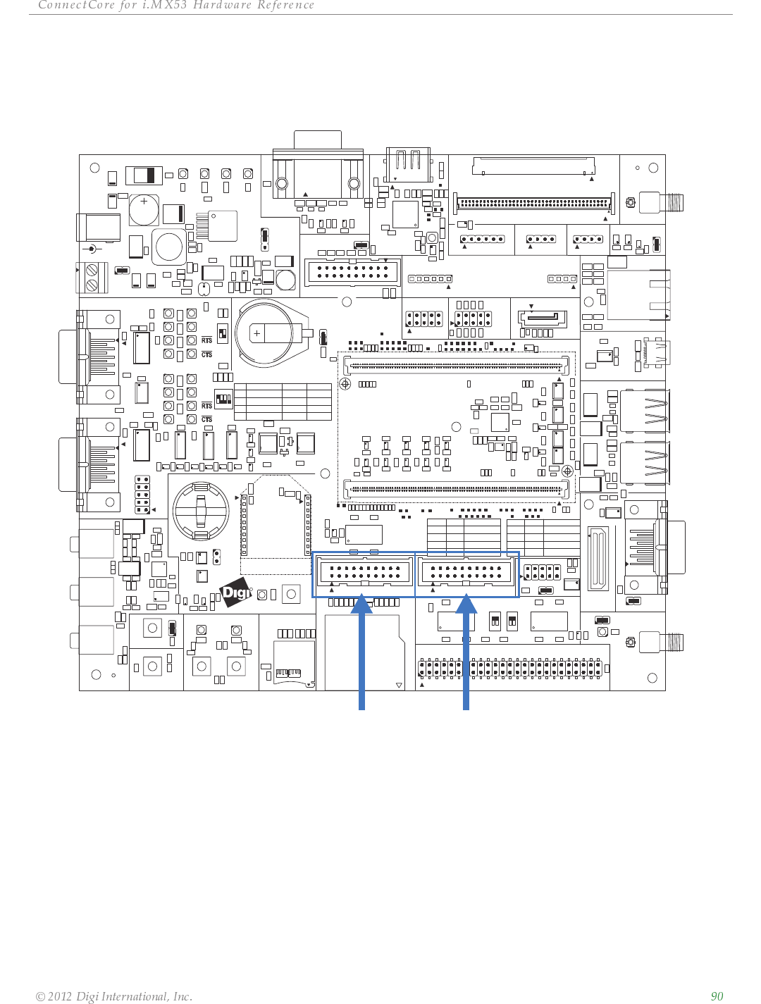
ȱ ȱ ȱ ȱ ȱ ȱ
ȱ ȱ ȱ ȱ ȱȱȱ
Camera Interfaces
The development board provides two camera interfaces connected to the camera sensor
interfaces (CSI) of the i.MX53 CPU. The I2C bus 3 of the ConnectCore for i.MX53 module is
used to configure and control connected cameras.
Two 2x10 pin headers, X15 and X16, are provided on the development board for optional Digi
camera application kits or customer specific camera hardware.
X15 connector for camera 1
X16 connector for camera 2
R
U3
U50
ON
41 32
S6
ON
1 2
S7
ON
1 2
S8
ON
1 2
S9
S5
S3
S13
S10
H9
H3
D1
U21
U11
Q2
U8 U33
U32
X18
P24 P22 P23
P29
X24
J1
J2
P1
P21
X19
X21
X45 X20
J24
J13
J17
J6
J20
J7
J9
U13
U52 U53
U51 U54
U7
U55
U56
U29
U28
U61
U19
U24
U38
U43
U42
U41
U4
U20U22
U17
U36
U18
U26
U6
U2
U15
JP6
JP20
JP1
JP3
JP10
JP4
JP12
JP5
J19
X32
X29
X28
X7
P20
J11
P19
R139
J27
J10
J8
L8
L26
L27
L21
L19
L22
L20
L25
L24
L18
L28
L29
L9
L12
L16
L3
L4
D5
V5 V6
D6
P12
P13
S12
V2
X30
X27
X31
X14
X16 X15
X13
U46
U10
U35U31U14 U40
LE59LE62LE63 LE61 LE41
LE57
LE60
LE58
LE7 LE6LE4LE8
LE51
LE49
LE40
LE43
LE42
LE44
LE47
LE48
LE45
LE46
LE12
LE50
J23
P14
P15
J15
J12
J18
V10
V11
O1 O2
R130
R131
R51
R133
R134
R28
R228
R56
R71
R75
R77
R74 R55R73
R59
R72
R57
R194
R96
R70
R18
R132
R14
R106
R108
R107
R105
R15
R11
+
C60
+
R52
R84
R41
C2
C1
P2
R45
R49
+
C3
+
R187
R189
R138
R159
R188
R5
R6
R7
C88
C87
C145
C86
R16
R42
R31
R39
R33
RN2
C85
R127
R8
R9
R36 R37
R34
R38
R35
R95
R89
R88
U37
U12
U16
U45
S2
C25
P4
C104
+
C49
C129
R53
C127
C48 C45
R182
C7 C6
L10
L6
L7
L5
R142
R86
+
C109
+
+
C108
+
+
C110
+
+
C111
+
C105
+
+
C90
+
R20
R181
R176
R12 R13
R85
R94
R195
R102
R101
C81
C103
C120
C169
C43
C53
C39
C27
C159
C161
C106
C46
C28
C162
C57
C155
R222
C163
C113 C114 C115
C126
C101
C125 C102
C69
C100
C95
C94
C59
C51
C56
C41
C26
C18
C50
C38
C83
C55
C58
C44
C89
C171
C78
C166
C165
C177
C84
C170
C52
C196
C118
C17
C123
C187
C98
C167
C117
C119
C79
C121
C188
C191
C179
R50
C99
C194
C97
C122
C189
C195
C158
C193
C186
C124
C96
C197
C80
C91
C93
C178
R199
C148
C147
C116
C107
C190
C192
C168
C112
R30
R17
R93
R27 R29
R135
R122
R10
U9
+
C20
+
R246
R247
C150
Y1
C153
C22
L23
R143
Y3
C151
C164
R23
C132
C134
C160
C131
C176
C175
C154
C174
C135
C133
C149
C70
C13
C12
C47
C61
C11
C71
C10
C62
C66
R118
R172
R4
R123
R61
R62
R63
R90
C23
R48
R117
R64
R76
R78
R141
R66
R79
R121
R65
R92
R91
R217
R21
R221
R100
R211
R110
R103
R99
R113
R2
R111
R126
R119
R25
R184
R104
R112
R1
R116
R220
R254
R154
R153
C157
C54
R137
L17
J5
U48
U47
U39
U34
U44
U25
U1 U23
U27
U5
R231
R204
R205
R218
R208
R289
R275
R274
R278
R287
R273
R261
R269
R206
R253
R202
R281
R203
R285
R290
R277
R284
R266
R257
R280
R282
R258
R259
R260
R276
R268
R22 R26
R19
R286
R283
R201
R262
R263
C128
R256
R265
R264
R207
R271
R158
R288
R272
R279
R291
R177
R213
R175
R179
R43
R178
R140
R209
R180
R232
R44
R47
R98
R58
R83
R24
R46
R270
R40
R174
R87
R109
R114
R3
R97
R129
R82
R124
R125
R152
R68
R151
R191
R227
R32
R193
R190
R196
R136
R230
R183
R192
R128
R120
R198
R229
R197
R162
C82
C37
C35
C15
C65 C67 C68
C36
C4
C5
C42
C29
C32
C34
C33
C64
C31
C156
C9
C63
C19
C30
C8
C14
C172
R81
R80
R186
R185
R67
R216
C152
C130
L11
L1
U57
LBL1
J4
R173
R214
C24
JP2
R292
C16
R69
R60
L30
R215
R171
U49
C21
U30
J3
C72
H1
R255
R293
U58
R54 C40
TP83TP85
TP61
TP90
TP114
TP67
TP66
TP115
TP69
TP116
TP71
TP117
TP74
TP78TP80
TP63
TP118
TP64
TP22
TP21
TP20
TP19
TP46
TP72
TP45
TP60
TP43
TP84
TP42
TP79
TP65
TP73
TP113
TP137
TP70
TP23
TP24TP81
TP47
TP48
TP77
TP76
TP75
TP93
TP38
TP49
TP52
TP51
TP39
TP41
TP25
TP82
TP89
TP87
TP62
TP29
TP30
TP31
TP28
TP91
TP33
TP35
TP57
TP26
TP37
TP88
TP86
TP68
TP58
TP36
TP92
TP27
TP44
X14
J17 P15
S8
CAN2
SATA
PWM
ON=
WLAN DISABLE
J19
J12
POWER
X27
ON=
P29
S9
S9
S5
_I2C
X21
CLOSE
RXD
J1
+3.3V_JS
SER DOWNLOAD
J18
+3.3V_MOD
DIGI
JTAG
S8
IDENT
DISABLED
USER
P22
+
LINE OUT
UART3 (TTL)
AUTO PWR DWN
J13
+
VCHRG
ON/CLOSE
P4
RESERVED
CAN1 TERMINATION
TXD
CLOSE
UART1 STATUS
X30
OPEN
P12
UART2 (MEI)
LE51
ETHERNET 1
SD/MMC
OPEN
X20
9V-30VDC
SPI
3
LE49
X15
RS485 MODE
+5V
DESCRIPTION
VBATT
J8
1
DISABLED
J10
MAIN POWER
OPEN
P24
J11
LE8
BOOT - SATA
ACTIVE
POS 1
OPEN
4
BUTTON 1
2-WIRE
S6
LVDS
LCD
OFF/OPEN
4-WIRE
ACTIVE
X32
POS
INT. BOOT
VGA
DESCRIPTION
2
MICRO SD
X28
WLAN PRIMARY
J27
ON=ENABLE
COIN CELL
X45
MICRO
1-WIRE
J15
INTERNATIONAL
ETHERNET 2
LE50
CAN1
WLAN SECONDARY
POS 2
J9
P1
OPEN
X29
J24
LED 2
LE4
X18
S13
PARALLEL LCD
S3
S12
XBEE MODULE
OFF
P2
J2
ON=AUTOBOOT
J20
i.MX53 MODULE
POS 1
J7
CLOSE OPEN
RXD
CLOSE
UART2 STATUS
BOOT - FUSES
X16
RESET
TERMINATION
P14
LINE IN
HDMI
X19
CLOSE
ASSOC
CLOSE CLOSE
BOOT - FLASH
POS 2
LED 1
CAN2 TERMINATION
S7
OPEN
X7
BOOT - uSD
BOOT - SD
J6
BUTTON 2
J23
P23
S2
LE6LE7
S10
KEYPAD
MODE
CAMERA 2
RS232
CONNECTCORE
RS422/485
EXT BATT
ENABLE EXT BATT
X24
TOUCH SELECTION
DESCRIPTION
ON
UART1 (CONSOLE)
+3.3VPOWER
LE12
CLOSE
DIGITAL I/O
TXD
PERIPHERAL CONNECTOR
CAMERA 1
BOOT CONF
USB OTG
USB HOST
ON=SJC-ONLY
AUDIO
J3
POE MODULE
P19
POE MODULE
BATT
OPEN
P20
P13
Camera 2
Connector, X16
Camera 1
Connector, X15
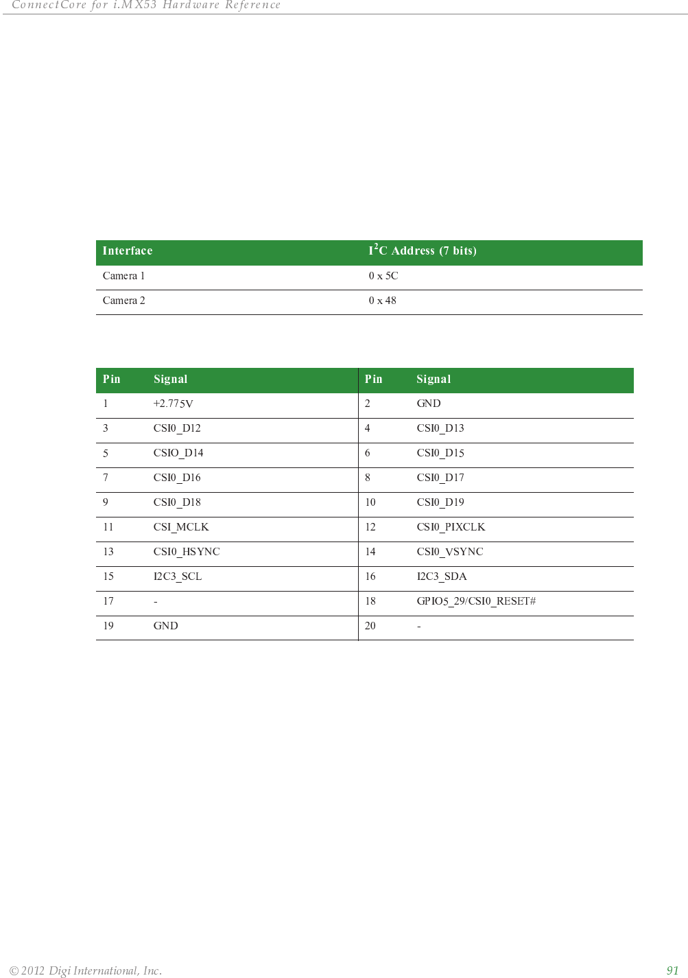
ȱ ȱ ȱ ȱ ȱ ȱ
ȱ ȱ ȱ ȱ ȱȱȱ
The camera 2 signals share the functionality in the development board with the bootstrap
interface and with the VGA interface. To avoid conflict between the camera 2/VGA signals
and the bootstrap interface, a delay circuit is provided in the board to disable the camera 2
and the VGA interfaces while the bootstrap configuration is being reading by the i.MX53 CPU.
Once the bootstrap configuration has been read the camera 2 and the VGA interfaces are
enabled. To avoid conflicts between the camera 2 and the VGA interface 0Ù resistors are
used to select the interface to be used. Please refer to the "Configuration Resistors" section
on page 79 for detailed information.
The following table shows the I2C device addresses of the Digi camera application kits:
X15 Pinout
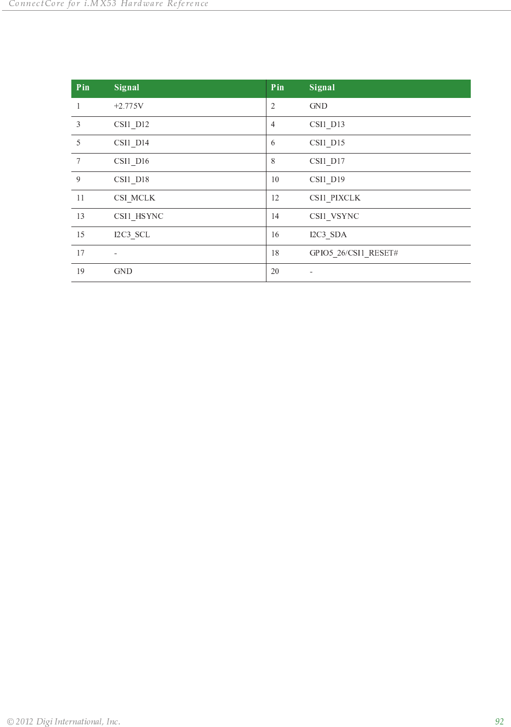
ȱ ȱ ȱ ȱ ȱ ȱ
ȱ ȱ ȱ ȱ ȱȱȱ
X16 Pinout
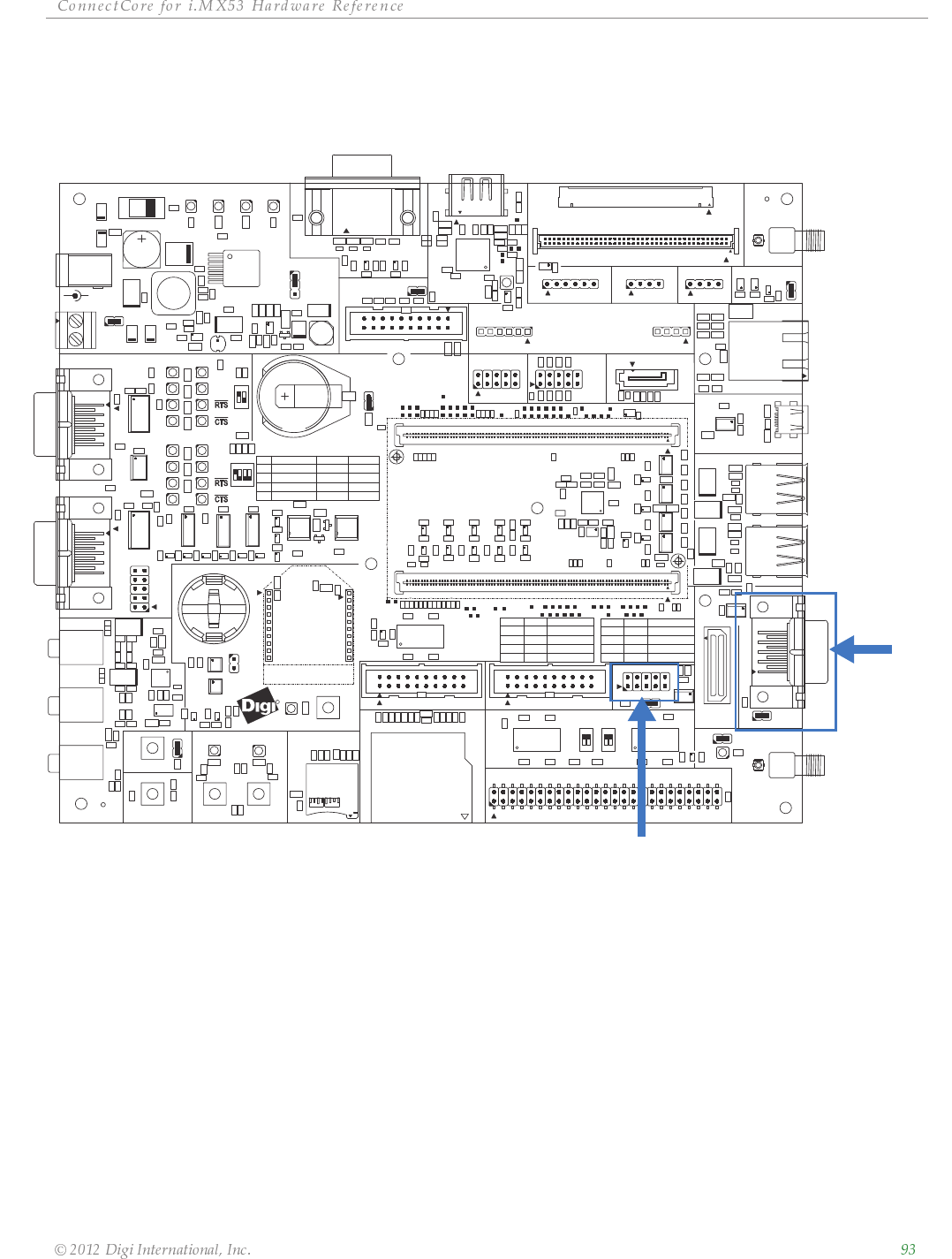
ȱ ȱ ȱ ȱ ȱ ȱ
ȱ ȱ ȱ ȱ ȱȱȱ
CAN Interface
R
U3
U50
ON
41 32
S6
ON
1 2
S7
ON
1 2
S8
ON
1 2
S9
S5
S3
S13
S10
H9
H3
D1
U21
U11
Q2
U8 U33
U32
X18
P24 P22 P23
P29
X24
J1
J2
P1
P21
X19
X21
X45 X20
J24
J13
J17
J6
J20
J7
J9
U13
U52 U53
U51 U54
U7
U55
U56
U29
U28
U61
U19
U24
U38
U43
U42
U41
U4
U20U22
U17
U36
U18
U26
U6
U2
U15
JP6
JP20
JP1
JP3
JP10
JP4
JP12
JP5
J19
X32
X29
X28
X7
P20
J11
P19
R139
J27
J10
J8
L8
L26
L27
L21
L19
L22
L20
L25
L24
L18
L28
L29
L9
L12
L16
L3
L4
D5
V5 V6
D6
P12
P13
S12
V2
X30
X27
X31
X14
X16 X15
X13
U46
U10
U35U31U14 U40
LE59LE62LE63 LE61 LE41
LE57
LE60
LE58
LE7 LE6LE4
LE8
LE51
LE49
LE40
LE43
LE42
LE44
LE47
LE48
LE45
LE46
LE12
LE50
J23
P14
P15
J15
J12
J18
V10
V11
O1 O2
R130
R131
R51
R133
R134
R28
R228
R56
R71
R75
R77
R74 R55R73
R59
R72
R57
R194
R96
R70
R18
R132
R14
R106
R108
R107
R105
R15
R11
+
C60
+
R52
R84
R41
C2
C1
P2
R45
R49
+
C3
+
R187
R189
R138
R159
R188
R5
R6
R7
C88
C87
C145
C86
R16
R42
R31
R39
R33
RN2
C85
R127
R8
R9
R36 R37
R34
R38
R35
R95
R89
R88
U37
U12
U16
U45
S2
C25
P4
C104
+
C49
C129
R53
C127
C48 C45
R182
C7 C6
L10
L6
L7
L5
R142
R86
+
C109
+
+
C108
+
+
C110
+
+
C111
+
C105
+
+
C90
+
R20
R181
R176
R12 R13
R85
R94
R195
R102
R101
C81
C103
C120
C169
C43
C53
C39
C27
C159
C161
C106
C46
C28
C162
C57
C155
R222
C163
C113 C114 C115
C126
C101
C125 C102
C69
C100
C95
C94
C59
C51
C56
C41
C26
C18
C50
C38
C83
C55
C58
C44
C89
C171
C78
C166
C165
C177
C84
C170
C52
C196
C118
C17
C123
C187
C98
C167
C117
C119
C79
C121
C188C191
C179
R50
C99
C194
C97
C122
C189
C195
C158
C193
C186
C124
C96
C197
C80
C91
C93
C178
R199
C148
C147
C116
C107
C190
C192
C168
C112
R30
R17
R93
R27 R29
R135
R122
R10
U9
+
C20
+
R246
R247
C150
Y1
C153
C22
L23
R143
Y3
C151
C164
R23
C132
C134
C160
C131
C176
C175
C154
C174
C135
C133
C149
C70
C13
C12
C47
C61
C11
C71
C10
C62
C66
R118
R172
R4
R123
R61
R62
R63
R90
C23
R48
R117
R64
R76
R78
R141
R66
R79
R121
R65
R92
R91
R217
R21
R221
R100
R211
R110
R103
R99
R113
R2
R111
R126
R119
R25
R184
R104
R112
R1
R116
R220
R254
R154
R153
C157
C54
R137
L17
J5
U48
U47
U39
U34
U44
U25
U1 U23
U27
U5
R231
R204
R205
R218
R208
R289
R275
R274
R278
R287
R273
R261
R269
R206
R253
R202
R281
R203
R285
R290
R277
R284
R266
R257
R280
R282
R258
R259
R260
R276
R268
R22 R26
R19
R286
R283
R201
R262
R263
C128
R256
R265
R264
R207
R271
R158
R288
R272
R279
R291
R177
R213
R175
R179
R43
R178
R140
R209
R180
R232
R44
R47
R98
R58
R83
R24
R46
R270
R40
R174
R87
R109
R114
R3
R97
R129
R82
R124
R125
R152
R68
R151
R191
R227
R32
R193
R190
R196
R136
R230
R183
R192
R128
R120
R198
R229
R197
R162
C82
C37
C35
C15
C65 C67 C68
C36
C4
C5
C42
C29
C32
C34
C33
C64
C31
C156
C9
C63
C19
C30
C8
C14
C172
R81
R80
R186
R185
R67
R216
C152
C130
L11
L1
U57
LBL1
J4
R173
R214
C24
JP2
R292
C16
R69
R60
L30
R215
R171
U49
C21
U30
J3
C72
H1
R255
R293
U58
R54 C40
TP83TP85
TP61
TP90
TP114
TP67
TP66
TP115
TP69
TP116
TP71
TP117
TP74
TP78TP80
TP63
TP118
TP64
TP22
TP21
TP20
TP19
TP46
TP72
TP45
TP60
TP43
TP84
TP42
TP79
TP65
TP73
TP113
TP137
TP70
TP23
TP24TP81
TP47
TP48
TP77
TP76
TP75
TP93
TP38
TP49
TP52
TP51
TP39TP41
TP25
TP82
TP89
TP87
TP62
TP29
TP30
TP31
TP28
TP91
TP33
TP35
TP57
TP26
TP37
TP88
TP86
TP68
TP58
TP36
TP92
TP27
TP44
X14
J17 P15
S8
CAN2
SATA
PWM
ON=
WLAN DISABLE
J19
J12
POWER
X27 ON=
P29
S9
S9
S5
_I2C
X21
CLOSE
RXD
J1
+3.3V_JS
SER DOWNLOAD
J18
+3.3V_MOD
DIGI
JTAG
S8
IDENT
DISABLED
USER
P22
+
LINE OUT
UART3 (TTL)
AUTO PWR DWN
J13
+
VCHRG
ON/CLOSE
P4
RESERVED
CAN1 TERMINATION
TXD
CLOSE
UART1 STATUS
X30
OPEN
P12
UART2 (MEI)
LE51
ETHERNET 1
SD/MMC
OPEN
X20
9V-30VDC
SPI
3
LE49
X15
RS485 MODE
+5V
DESCRIPTION
VBATT
J8
1
DISABLED
J10
MAIN POWER
OPEN
P24
J11
LE8
BOOT - SATA
ACTIVE
POS 1
OPEN
4
BUTTON 1
2-WIRE
S6
LVDS
LCD
OFF/OPEN
4-WIRE
ACTIVE
X32
POS
INT. BOOT
VGA
DESCRIPTION
2
MICRO SD
X28
WLAN PRIMARY
J27
ON=ENABLE
COIN CELL
X45
MICRO
1-WIRE
J15
INTERNATIONAL
ETHERNET 2
LE50
CAN1
WLAN SECONDARY
POS 2
J9
P1
OPEN
X29
J24
LED 2
LE4
X18
S13
PARALLEL LCD
S3
S12
XBEE MODULE
OFF
P2
J2
ON=AUTOBOOT
J20
i.MX53 MODULE
POS 1
J7
CLOSE OPEN
RXD
CLOSE
UART2 STATUS
BOOT - FUSES
X16
RESET
TERMINATION
P14
LINE IN
HDMI
X19
CLOSE
ASSOC
CLOSE CLOSE
BOOT - FLASH
POS 2
LED 1
CAN2 TERMINATION
S7
OPEN
X7
BOOT - uSD
BOOT - SD
J6
BUTTON 2
J23
P23
S2
LE6LE7
S10
KEYPAD
MODE
CAMERA 2
RS232
CONNECTCORE
RS422/485
EXT BATT
ENABLE EXT BATT
X24
TOUCH SELECTION
DESCRIPTION
ON
UART1 (CONSOLE)
+3.3VPOWER
LE12
CLOSE
DIGITAL I/O
TXD
PERIPHERAL CONNECTOR
CAMERA 1
BOOT CONF
USB OTG
USB HOST
ON=SJC-ONLY
AUDIO
J3
POE MODULE
P19
POE MODULE
BATT
OPEN
P20
P13
CAN 1,
X31
CAN 2, X21
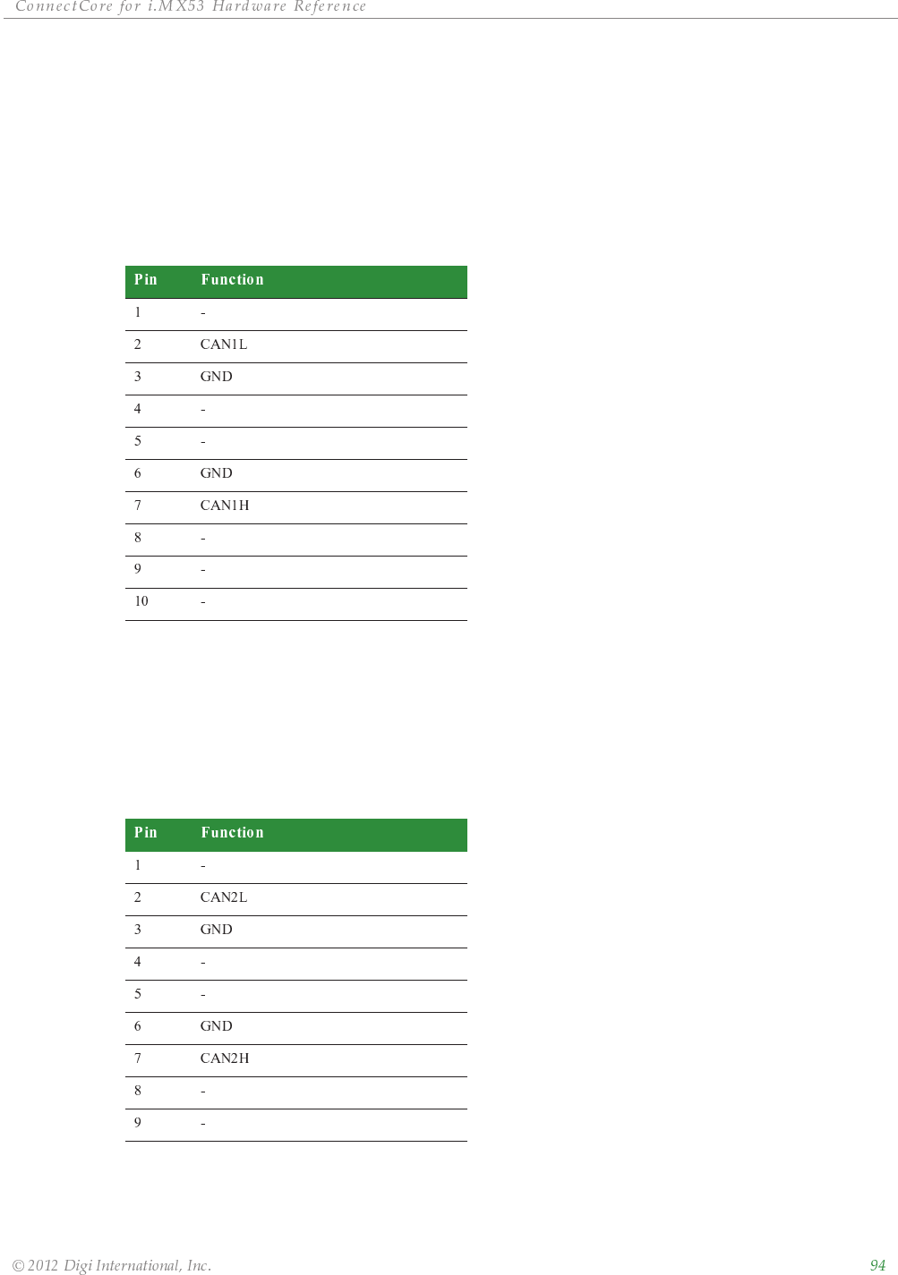
ȱ ȱ ȱ ȱ ȱ ȱ
ȱ ȱ ȱ ȱ ȱȱȱ
CAN 1, X31
The CAN 1 connector X31, is a DB-9 male connector. One 120 ohm termination resistor can be
connected to the output lines of the CAN 1 bus. The termination resistor can be connected or
disconnected using the jumper J7. Refer to the “Jumpers” section on page 77 for more
information.
CAN 1 pins are allocated as shown:
CAN 2, X21
The CAN 2 connector X21, is a 2x5 pin header. One 120 ohm termination resistor can be
connected to the output lines of the CAN 2 bus. The termination resistor can be connected or
disconnected using the jumper J9. Refer to the “Jumpers” section on page 77 for more
information.
CAN 2 pins are allocated as shown:
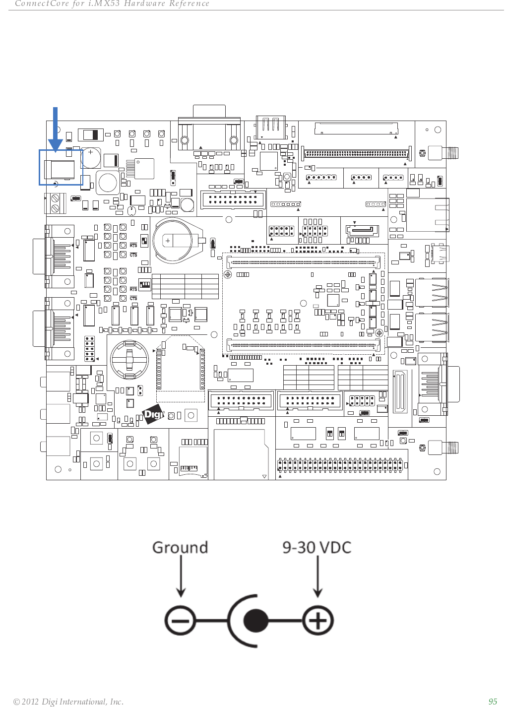
ȱ ȱ ȱ ȱ ȱ ȱ
ȱ ȱ ȱ ȱ ȱȱȱ
Charger Power Connector
The charger power connector (X24) is a barrel connector for the development board’s
9-30VDC power supply. The figure below shows the polarity.
R
U3
U50
ON
41 32
S6
ON
1 2
S7
ON
1 2
S8
ON
1 2
S9
S5
S3
S13
S10
H9
H3
D1
U21
U11
Q2
U8 U33
U32
X18
P24 P22 P23
P29
X24
J1
J2
P1
P21
X19
X21
X45 X20
J24
J13
J17
J6
J20
J7
J9
U13
U52 U53
U51 U54
U7
U55
U56
U29
U28
U61
U19
U24
U38
U43
U42
U41
U4
U20U22
U17
U36
U18
U26
U6
U2
U15
JP6
JP20
JP1
JP3
JP10
JP4
JP12
JP5
J19
X32
X29
X28
X7
P20
J11
P19
R139
J27
J10
J8
L8
L26
L27
L21
L19
L22
L20
L25
L24
L18
L28
L29
L9
L12
L16
L3
L4
D5
V5 V6
D6
P12
P13
S12
V2
X30
X27
X31
X14
X16 X15
X13
U46
U10
U35U31U14 U40
LE59LE62LE63 LE61 LE41
LE57
LE60
LE58
LE7 LE6LE4LE8
LE51
LE49
LE40
LE43
LE42
LE44
LE47
LE48
LE45
LE46
LE12
LE50
J23
P14
P15
J15
J12
J18
V10
V11
O1 O2
R130
R131
R51
R133
R134
R28
R228
R56
R71
R75
R77
R74 R55R73
R59
R72
R57
R194
R96
R70
R18
R132
R14
R106
R108
R107
R105
R15
R11
+
C60
+
R52
R84
R41
C2
C1
P2
R45
R49
+
C3
+
R187
R189
R138
R159
R188
R5
R6
R7
C88
C87
C145
C86
R16
R42
R31
R39
R33
RN2
C85
R127
R8
R9
R36 R37
R34
R38
R35
R95
R89
R88
U37
U12
U16
U45
S2
C25
P4
C104
+
C49
C129
R53
C127
C48 C45
R182
C7 C6
L10
L6
L7
L5
R142
R86
+
C109
+
+
C108
+
+
C110
+
+
C111
+
C105
+
+
C90
+
R20
R181
R176
R12 R13
R85
R94
R195
R102
R101
C81
C103
C120
C169
C43
C53
C39
C27
C159
C161
C106
C46
C28
C162
C57
C155
R222
C163
C113 C114 C115
C126
C101
C125 C102
C69
C100
C95
C94
C59
C51
C56
C41
C26
C18
C50
C38
C83
C55
C58
C44
C89
C171
C78
C166
C165
C177
C84
C170
C52
C196
C118
C17
C123
C187
C98
C167
C117
C119
C79
C121
C188
C191
C179
R50
C99
C194
C97
C122
C189
C195
C158
C193
C186
C124
C96
C197
C80
C91
C93
C178
R199
C148
C147
C116
C107
C190
C192
C168
C112
R30
R17
R93
R27 R29
R135
R122
R10
U9
+
C20
+
R246
R247
C150
Y1
C153
C22
L23
R143
Y3
C151
C164
R23
C132
C134
C160
C131
C176
C175
C154
C174
C135
C133
C149
C70
C13
C12
C47
C61
C11
C71
C10
C62
C66
R118
R172
R4
R123
R61
R62
R63
R90
C23
R48
R117
R64
R76
R78
R141
R66
R79
R121
R65
R92
R91
R217
R21
R221
R100
R211
R110
R103
R99
R113
R2
R111
R126
R119
R25
R184
R104
R112
R1
R116
R220
R254
R154
R153
C157
C54
R137
L17
J5
U48
U47
U39
U34
U44
U25
U1 U23
U27
U5
R231
R204
R205
R218
R208
R289
R275
R274
R278
R287
R273
R261
R269
R206
R253
R202
R281
R203
R285
R290
R277
R284
R266
R257
R280
R282
R258
R259
R260
R276
R268
R22 R26
R19
R286
R283
R201
R262
R263
C128
R256
R265
R264
R207
R271
R158
R288
R272
R279
R291
R177
R213
R175
R179
R43
R178
R140
R209
R180
R232
R44
R47
R98
R58
R83
R24
R46
R270
R40
R174
R87
R109
R114
R3
R97
R129
R82
R124
R125
R152
R68
R151
R191
R227
R32
R193
R190
R196
R136
R230
R183
R192
R128
R120
R198
R229
R197
R162
C82
C37
C35
C15
C65 C67 C68
C36
C4
C5
C42
C29
C32
C34
C33
C64
C31
C156
C9
C63
C19
C30
C8
C14
C172
R81
R80
R186
R185
R67
R216
C152
C130
L11
L1
U57
LBL1
J4
R173
R214
C24
JP2
R292
C16
R69
R60
L30
R215
R171
U49
C21
U30
J3
C72
H1
R255
R293
U58
R54 C40
TP83TP85
TP61
TP90
TP114
TP67
TP66
TP115
TP69
TP116
TP71
TP117
TP74
TP78TP80
TP63
TP118
TP64
TP22
TP21
TP20
TP19
TP46
TP72
TP45
TP60
TP43
TP84
TP42
TP79
TP65
TP73
TP113
TP137
TP70
TP23
TP24TP81
TP47
TP48
TP77
TP76
TP75
TP93
TP38
TP49
TP52
TP51
TP39TP41
TP25
TP82
TP89
TP87
TP62
TP29
TP30
TP31
TP28
TP91
TP33
TP35
TP57
TP26
TP37
TP88
TP86
TP68
TP58
TP36
TP92
TP27
TP44
X14
J17 P15
S8
CAN2
SATA
PWM
ON=
WLAN DISABLE
J19
J12
POWER
X27 ON=
P29
S9
S9
S5
_I2C
X21
CLOSE
RXD
J1
+3.3V_JS
SER DOWNLOAD
J18
+3.3V_MOD
DIGI
JTAG
S8
IDENT
DISABLED
USER
P22
+
LINE OUT
UART3 (TTL)
AUTO PWR DWN
J13
+
VCHRG
ON/CLOSE
P4
RESERVED
CAN1 TERMINATION
TXD
CLOSE
UART1 STATUS
X30
OPEN
P12
UART2 (MEI)
LE51
ETHERNET 1
SD/MMC
OPEN
X20
9V-30VDC
SPI
3
LE49
X15
RS485 MODE
+5V
DESCRIPTION
VBATT
J8
1
DISABLED
J10
MAIN POWER
OPEN
P24
J11
LE8
BOOT - SATA
ACTIVE
POS 1
OPEN
4
BUTTON 1
2-WIRE
S6
LVDS
LCD
OFF/OPEN
4-WIRE
ACTIVE
X32
POS
INT. BOOT
VGA
DESCRIPTION
2
MICRO SD
X28
WLAN PRIMARY
J27
ON=ENABLE
COIN CELL
X45
MICRO
1-WIRE
J15
INTERNATIONAL
ETHERNET 2
LE50
CAN1
WLAN SECONDARY
POS 2
J9
P1
OPEN
X29
J24
LED 2
LE4
X18
S13
PARALLEL LCD
S3
S12
XBEE MODULE
OFF
P2
J2
ON=AUTOBOOT
J20
i.MX53 MODULE
POS 1
J7
CLOSE OPEN
RXD
CLOSE
UART2 STATUS
BOOT - FUSES
X16
RESET
TERMINATION
P14
LINE IN
HDMI
X19
CLOSE
ASSOC
CLOSE CLOSE
BOOT - FLASH
POS 2
LED 1
CAN2 TERMINATION
S7
OPEN
X7
BOOT - uSD
BOOT - SD
J6
BUTTON 2
J23
P23
S2
LE6LE7
S10
KEYPAD
MODE
CAMERA 2
RS232
CONNECTCORE
RS422/485
EXT BATT
ENABLE EXT BATT
X24
TOUCH SELECTION
DESCRIPTION
ON
UART1 (CONSOLE)
+3.3VPOWER
LE12
CLOSE
DIGITAL I/O
TXD
PERIPHERAL CONNECTOR
CAMERA 1
BOOT CONF
USB OTG
USB HOST
ON=SJC-ONLY
AUDIO
J3
POE MODULE
P19
POE MODULE
BATT
OPEN
P20
P13
Charger Power
Connector, X24
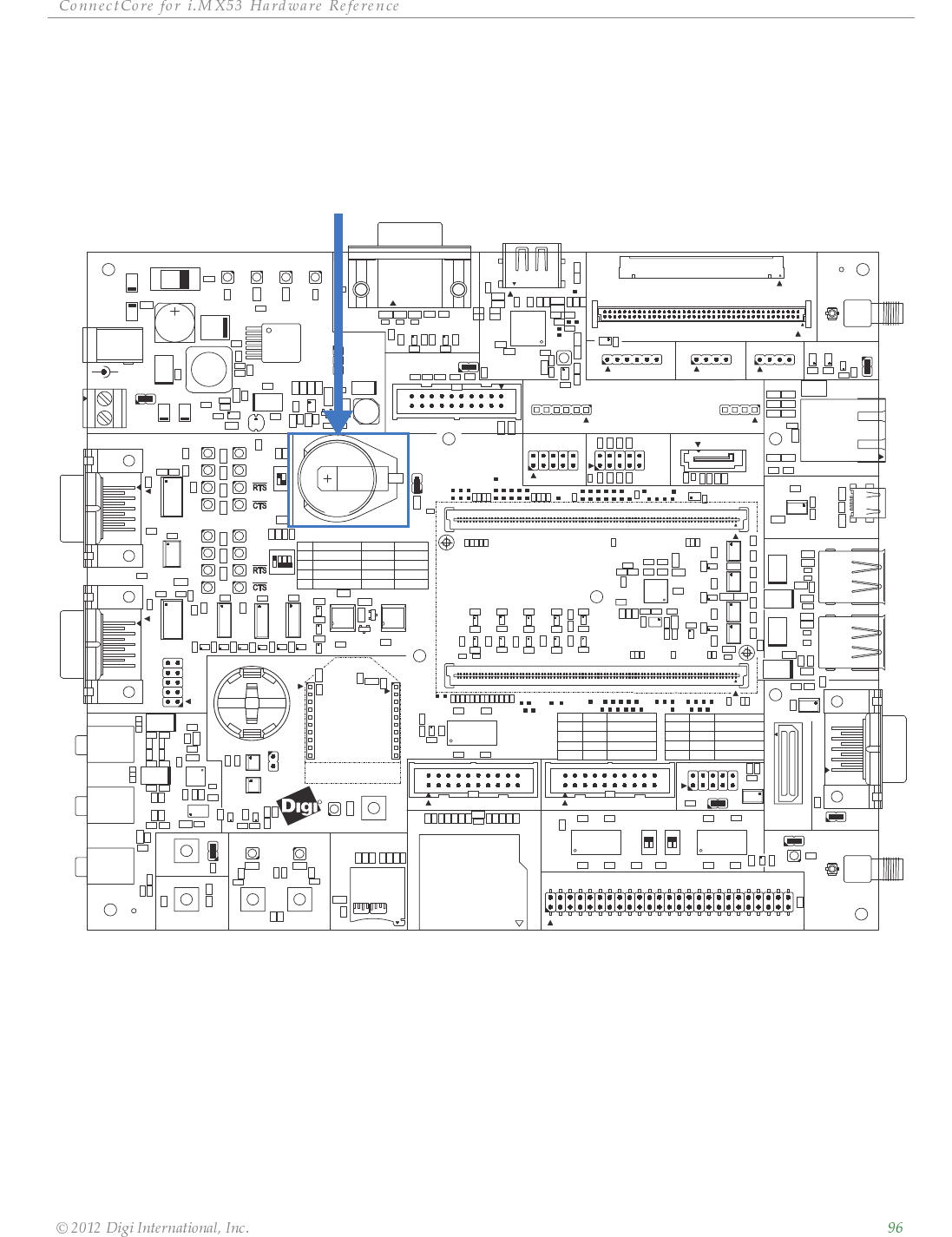
ȱ ȱ ȱ ȱ ȱ ȱ
ȱ ȱ ȱ ȱ ȱȱȱ
Coin Cell Battery
The development board provides a coin cell battery to back up the module’s integrated RTC
while main power is disconnected. Jumper J3 connects/disconnects the coin cell power
source.
R
U3
U50
ON
41 32
S6
ON
1 2
S7
ON
1 2
S8
ON
1 2
S9
S5
S3
S13
S10
H9
H3
D1
U21
U11
Q2
U8 U33
U32
X18
P24 P22 P23
P29
X24
J1
J2
P1
P21
X19
X21
X45 X20
J24
J13
J17
J6
J20
J7
J9
U13
U52 U53
U51 U54
U7
U55
U56
U29
U28
U61
U19
U24
U38
U43
U42
U41
U4
U20U22
U17
U36
U18
U26
U6
U2
U15
JP6
JP20
JP1
JP3
JP10
JP4
JP12
JP5
J19
X32
X29
X28
X7
P20
J11
P19
R139
J27
J10
J8
L8
L26
L27
L21
L19
L22
L20
L25
L24
L18
L28
L29
L9
L12
L16
L3
L4
D5
V5 V6
D6
P12
P13
S12
V2
X30
X27
X31
X14
X16 X15
X13
U46
U10
U35U31U14 U40
LE59LE62LE63 LE61 LE41
LE57
LE60
LE58
LE7 LE6LE4
LE8
LE51
LE49
LE40
LE43
LE42
LE44
LE47
LE48
LE45
LE46
LE12
LE50
J23
P14
P15
J15
J12
J18
V10
V11
O1 O2
R130
R131
R51
R133
R134
R28
R228
R56
R71
R75
R77
R74 R55R73
R59
R72
R57
R194
R96
R70
R18
R132
R14
R106
R108
R107
R105
R15
R11
+
C60
+
R52
R84
R41
C2
C1
P2
R45
R49
+
C3
+
R187
R189
R138
R159
R188
R5
R6
R7
C88
C87
C145
C86
R16
R42
R31
R39
R33
RN2
C85
R127
R8
R9
R36 R37
R34
R38
R35
R95
R89
R88
U37
U12
U16
U45
S2
C25
P4
C104
+
C49
C129
R53
C127
C48 C45
R182
C7 C6
L10
L6
L7
L5
R142
R86
+
C109
+
+
C108
+
+
C110
+
+
C111
+
C105
+
+
C90
+
R20
R181
R176
R12 R13
R85
R94
R195
R102
R101
C81
C103
C120
C169
C43
C53
C39
C27
C159
C161
C106
C46
C28
C162
C57
C155
R222
C163
C113 C114 C115
C126
C101
C125 C102
C69
C100
C95
C94
C59
C51
C56
C41
C26
C18
C50
C38
C83
C55
C58
C44
C89
C171
C78
C166
C165
C177
C84
C170
C52
C196
C118
C17
C123
C187
C98
C167
C117
C119
C79
C121
C188
C191
C179
R50
C99
C194
C97
C122
C189
C195
C158
C193
C186
C124
C96
C197
C80
C91
C93
C178
R199
C148
C147
C116
C107
C190
C192
C168
C112
R30
R17
R93
R27 R29
R135
R122
R10
U9
+
C20
+
R246
R247
C150
Y1
C153
C22
L23
R143
Y3
C151
C164
R23
C132
C134
C160
C131
C176
C175
C154
C174
C135
C133
C149
C70
C13
C12
C47
C61
C11
C71
C10
C62
C66
R118
R172
R4
R123
R61
R62
R63
R90
C23
R48
R117
R64
R76
R78
R141
R66
R79
R121
R65
R92
R91
R217
R21
R221
R100
R211
R110
R103
R99
R113
R2
R111
R126
R119
R25
R184
R104
R112
R1
R116
R220
R254
R154
R153
C157
C54
R137
L17
J5
U48
U47
U39
U34
U44
U25
U1 U23
U27
U5
R231
R204
R205
R218
R208
R289
R275
R274
R278
R287
R273
R261
R269
R206
R253
R202
R281
R203
R285
R290
R277
R284
R266
R257
R280
R282
R258
R259
R260
R276
R268
R22 R26
R19
R286
R283
R201
R262
R263
C128
R256
R265
R264
R207
R271
R158
R288
R272
R279
R291
R177
R213
R175
R179
R43
R178
R140
R209
R180
R232
R44
R47
R98
R58
R83
R24
R46
R270
R40
R174
R87
R109
R114
R3
R97
R129
R82
R124
R125
R152
R68
R151
R191
R227
R32
R193
R190
R196
R136
R230
R183
R192
R128
R120
R198
R229
R197
R162
C82
C37
C35
C15
C65 C67 C68
C36
C4
C5
C42
C29
C32
C34
C33
C64
C31
C156
C9
C63
C19
C30
C8
C14
C172
R81
R80
R186
R185
R67
R216
C152
C130
L11
L1
U57
LBL1
J4
R173
R214
C24
JP2
R292
C16
R69
R60
L30
R215
R171
U49
C21
U30
J3
C72
H1
R255
R293
U58
R54 C40
TP83TP85
TP61
TP90
TP114
TP67
TP66
TP115
TP69
TP116
TP71
TP117
TP74
TP78TP80
TP63
TP118
TP64
TP22
TP21
TP20
TP19
TP46
TP72
TP45
TP60
TP43
TP84
TP42
TP79
TP65
TP73
TP113
TP137
TP70
TP23
TP24TP81
TP47
TP48
TP77
TP76
TP75
TP93
TP38
TP49
TP52
TP51
TP39
TP41
TP25
TP82
TP89
TP87
TP62
TP29
TP30
TP31
TP28
TP91
TP33
TP35
TP57
TP26
TP37
TP88
TP86
TP68
TP58
TP36
TP92
TP27
TP44
X14
J17 P15
S8
CAN2
SATA
PWM
ON=
WLAN DISABLE
J19
J12
POWER
X27
ON=
P29
S9
S9
S5
_I2C
X21
CLOSE
RXD
J1
+3.3V_JS
SER DOWNLOAD
J18
+3.3V_MOD
DIGI
JTAG
S8
IDENT
DISABLED
USER
P22
+
LINE OUT
UART3 (TTL)
AUTO PWR DWN
J13
+
VCHRG
ON/CLOSE
P4
RESERVED
CAN1 TERMINATION
TXD
CLOSE
UART1 STATUS
X30
OPEN
P12
UART2 (MEI)
LE51
ETHERNET 1
SD/MMC
OPEN
X20
9V-30VDC
SPI
3
LE49
X15
RS485 MODE
+5V
DESCRIPTION
VBATT
J8
1
DISABLED
J10
MAIN POWER
OPEN
P24
J11
LE8
BOOT - SATA
ACTIVE
POS 1
OPEN
4
BUTTON 1
2-WIRE
S6
LVDS
LCD
OFF/OPEN
4-WIRE
ACTIVE
X32
POS
INT. BOOT
VGA
DESCRIPTION
2
MICRO SD
X28
WLAN PRIMARY
J27
ON=ENABLE
COIN CELL
X45
MICRO
1-WIRE
J15
INTERNATIONAL
ETHERNET 2
LE50
CAN1
WLAN SECONDARY
POS 2
J9
P1
OPEN
X29
J24
LED 2
LE4
X18
S13
PARALLEL LCD
S3
S12
XBEE MODULE
OFF
P2
J2
ON=AUTOBOOT
J20
i.MX53 MODULE
POS 1
J7
CLOSE OPEN
RXD
CLOSE
UART2 STATUS
BOOT - FUSES
X16
RESET
TERMINATION
P14
LINE IN
HDMI
X19
CLOSE
ASSOC
CLOSE CLOSE
BOOT - FLASH
POS 2
LED 1
CAN2 TERMINATION
S7
OPEN
X7
BOOT - uSD
BOOT - SD
J6
BUTTON 2
J23
P23
S2
LE6LE7
S10
KEYPAD
MODE
CAMERA 2
RS232
CONNECTCORE
RS422/485
EXT BATT
ENABLE EXT BATT
X24
TOUCH SELECTION
DESCRIPTION
ON
UART1 (CONSOLE)
+3.3VPOWER
LE12
CLOSE
DIGITAL I/O
TXD
PERIPHERAL CONNECTOR
CAMERA 1
BOOT CONF
USB OTG
USB HOST
ON=SJC-ONLY
AUDIO
J3
POE MODULE
P19
POE MODULE
BATT
OPEN
P20
P13
Coin Cell Battery
Holder, H1
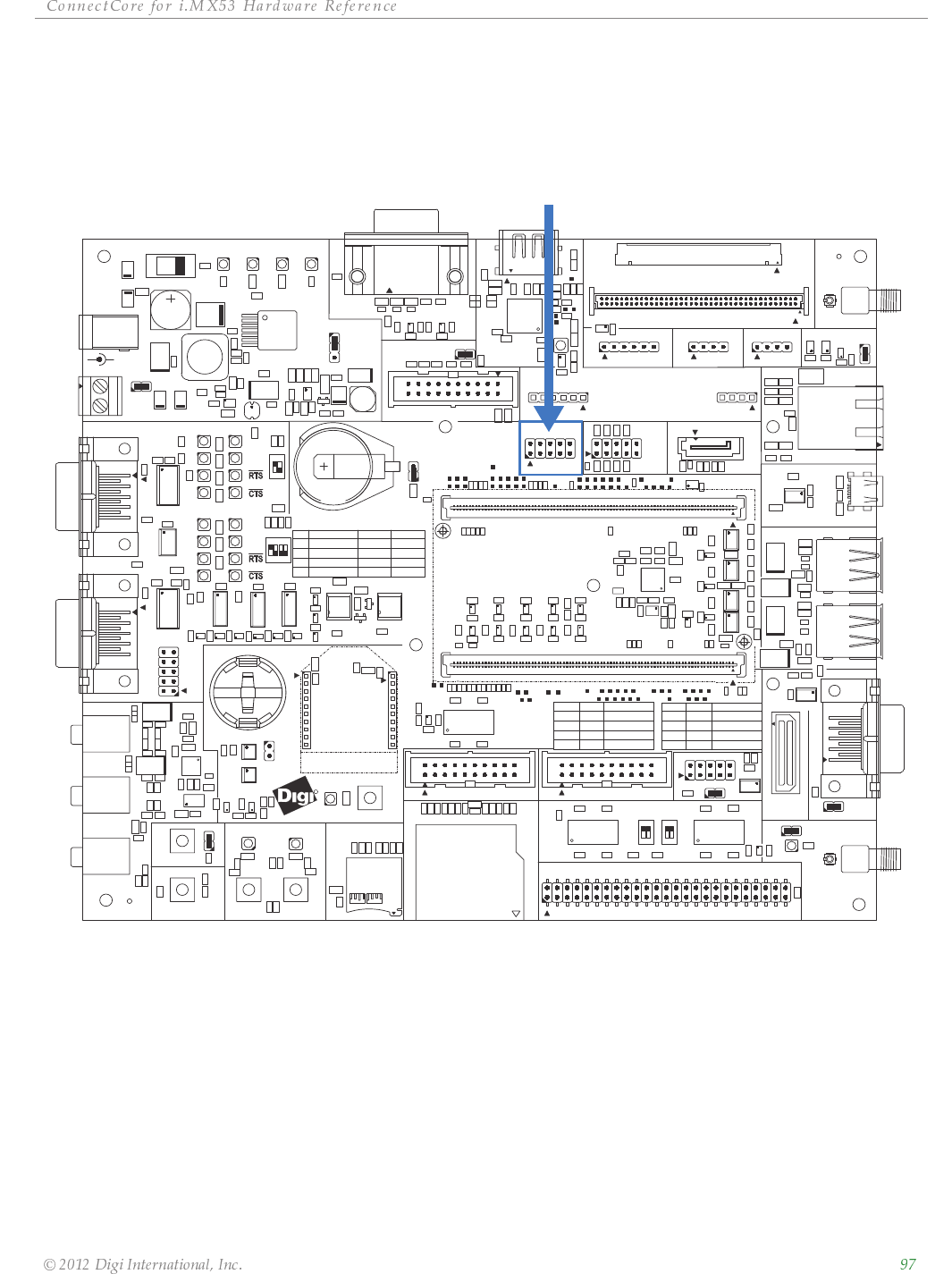
ȱ ȱ ȱ ȱ ȱ ȱ
ȱ ȱ ȱ ȱ ȱȱȱ
Digital IO Interface
R
U3
U50
ON
41 32
S6
ON
1 2
S7
ON
1 2
S8
ON
1 2
S9
S5
S3
S13
S10
H9
H3
D1
U21
U11
Q2
U8 U33
U32
X18
P24 P22 P23
P29
X24
J1
J2
P1
P21
X19
X21
X45 X20
J24
J13
J17
J6
J20
J7
J9
U13
U52 U53
U51 U54
U7
U55
U56
U29
U28
U61
U19
U24
U38
U43
U42
U41
U4
U20U22
U17
U36
U18
U26
U6
U2
U15
JP6
JP20
JP1
JP3
JP10
JP4
JP12
JP5
J19
X32
X29
X28
X7
P20
J11
P19
R139
J27
J10
J8
L8
L26
L27
L21
L19
L22
L20
L25
L24
L18
L28
L29
L9
L12
L16
L3
L4
D5
V5 V6
D6
P12
P13
S12
V2
X30
X27
X31
X14
X16 X15
X13
U46
U10
U35U31U14 U40
LE59LE62LE63 LE61 LE41
LE57
LE60
LE58
LE7 LE6LE4
LE8
LE51
LE49
LE40
LE43
LE42
LE44
LE47
LE48
LE45
LE46
LE12
LE50
J23
P14
P15
J15
J12
J18
V10
V11
O1 O2
R130
R131
R51
R133
R134
R28
R228
R56
R71
R75
R77
R74 R55R73
R59
R72
R57
R194
R96
R70
R18
R132
R14
R106
R108
R107
R105
R15
R11
+
C60
+
R52
R84
R41
C2
C1
P2
R45
R49
+
C3
+
R187
R189
R138
R159
R188
R5
R6
R7
C88
C87
C145
C86
R16
R42
R31
R39
R33
RN2
C85
R127
R8
R9
R36 R37
R34
R38
R35
R95
R89
R88
U37
U12
U16
U45
S2
C25
P4
C104
+
C49
C129
R53
C127
C48 C45
R182
C7 C6
L10
L6
L7
L5
R142
R86
+
C109
+
+
C108
+
+
C110
+
+
C111
+
C105
+
+
C90
+
R20
R181
R176
R12 R13
R85
R94
R195
R102
R101
C81
C103
C120
C169
C43
C53
C39
C27
C159
C161
C106
C46
C28
C162
C57
C155
R222
C163
C113 C114 C115
C126
C101
C125 C102
C69
C100
C95
C94
C59
C51
C56
C41
C26
C18
C50
C38
C83
C55
C58
C44
C89
C171
C78
C166
C165
C177
C84
C170
C52
C196
C118
C17
C123
C187
C98
C167
C117
C119
C79
C121
C188
C191
C179
R50
C99
C194
C97
C122
C189
C195
C158
C193
C186
C124
C96
C197
C80
C91
C93
C178
R199
C148
C147
C116
C107
C190
C192
C168
C112
R30
R17
R93
R27 R29
R135
R122
R10
U9
+
C20
+
R246
R247
C150
Y1
C153
C22
L23
R143
Y3
C151
C164
R23
C132
C134
C160
C131
C176
C175
C154
C174
C135
C133
C149
C70
C13
C12
C47
C61
C11
C71
C10
C62
C66
R118
R172
R4
R123
R61
R62
R63
R90
C23
R48
R117
R64
R76
R78
R141
R66
R79
R121
R65
R92
R91
R217
R21
R221
R100
R211
R110
R103
R99
R113
R2
R111
R126
R119
R25
R184
R104
R112
R1
R116
R220
R254
R154
R153
C157
C54
R137
L17
J5
U48
U47
U39
U34
U44
U25
U1 U23
U27
U5
R231
R204
R205
R218
R208
R289
R275
R274
R278
R287
R273
R261
R269
R206
R253
R202
R281
R203
R285
R290
R277
R284
R266
R257
R280
R282
R258
R259
R260
R276
R268
R22 R26
R19
R286
R283
R201
R262
R263
C128
R256
R265
R264
R207
R271
R158
R288
R272
R279
R291
R177
R213
R175
R179
R43
R178
R140
R209
R180
R232
R44
R47
R98
R58
R83
R24
R46
R270
R40
R174
R87
R109
R114
R3
R97
R129
R82
R124
R125
R152
R68
R151
R191
R227
R32
R193
R190
R196
R136
R230
R183
R192
R128
R120
R198
R229
R197
R162
C82
C37
C35
C15
C65 C67 C68
C36
C4
C5
C42
C29
C32
C34
C33
C64
C31
C156
C9
C63
C19
C30
C8
C14
C172
R81
R80
R186
R185
R67
R216
C152
C130
L11
L1
U57
LBL1
J4
R173
R214
C24
JP2
R292
C16
R69
R60
L30
R215
R171
U49
C21
U30
J3
C72
H1
R255
R293
U58
R54 C40
TP83TP85
TP61
TP90
TP114
TP67
TP66
TP115
TP69
TP116
TP71
TP117
TP74
TP78TP80
TP63
TP118
TP64
TP22
TP21
TP20
TP19
TP46
TP72
TP45
TP60
TP43
TP84
TP42
TP79
TP65
TP73
TP113
TP137
TP70
TP23
TP24TP81
TP47
TP48
TP77
TP76
TP75
TP93
TP38
TP49
TP52
TP51
TP39TP41
TP25
TP82
TP89
TP87
TP62
TP29
TP30
TP31
TP28
TP91
TP33
TP35
TP57
TP26
TP37
TP88
TP86
TP68
TP58
TP36
TP92
TP27
TP44
X14
J17 P15
S8
CAN2
SATA
PWM
ON=
WLAN DISABLE
J19
J12
POWER
X27 ON=
P29
S9
S9
S5
_I2C
X21
CLOSE
RXD
J1
+3.3V_JS
SER DOWNLOAD
J18
+3.3V_MOD
DIGI
JTAG
S8
IDENT
DISABLED
USER
P22
+
LINE OUT
UART3 (TTL)
AUTO PWR DWN
J13
+
VCHRG
ON/CLOSE
P4
RESERVED
CAN1 TERMINATION
TXD
CLOSE
UART1 STATUS
X30
OPEN
P12
UART2 (MEI)
LE51
ETHERNET 1
SD/MMC
OPEN
X20
9V-30VDC
SPI
3
LE49
X15
RS485 MODE
+5V
DESCRIPTION
VBATT
J8
1
DISABLED
J10
MAIN POWER
OPEN
P24
J11
LE8
BOOT - SATA
ACTIVE
POS 1
OPEN
4
BUTTON 1
2-WIRE
S6
LVDS
LCD
OFF/OPEN
4-WIRE
ACTIVE
X32
POS
INT. BOOT
VGA
DESCRIPTION
2
MICRO SD
X28
WLAN PRIMARY
J27
ON=ENABLE
COIN CELL
X45
MICRO
1-WIRE
J15
INTERNATIONAL
ETHERNET 2
LE50
CAN1
WLAN SECONDARY
POS 2
J9
P1
OPEN
X29
J24
LED 2
LE4
X18
S13
PARALLEL LCD
S3
S12
XBEE MODULE
OFF
P2
J2
ON=AUTOBOOT
J20
i.MX53 MODULE
POS 1
J7
CLOSE OPEN
RXD
CLOSE
UART2 STATUS
BOOT - FUSES
X16
RESET
TERMINATION
P14
LINE IN
HDMI
X19
CLOSE
ASSOC
CLOSE CLOSE
BOOT - FLASH
POS 2
LED 1
CAN2 TERMINATION
S7
OPEN
X7
BOOT - uSD
BOOT - SD
J6
BUTTON 2
J23
P23
S2
LE6LE7
S10
KEYPAD
MODE
CAMERA 2
RS232
CONNECTCORE
RS422/485
EXT BATT
ENABLE EXT BATT
X24
TOUCH SELECTION
DESCRIPTION
ON
UART1 (CONSOLE)
+3.3VPOWER
LE12
CLOSE
DIGITAL I/O
TXD
PERIPHERAL CONNECTOR
CAMERA 1
BOOT CONF
USB OTG
USB HOST
ON=SJC-ONLY
AUDIO
J3
POE MODULE
P19
POE MODULE
BATT
OPEN
P20
P13
Digital I/O
Connector, X45
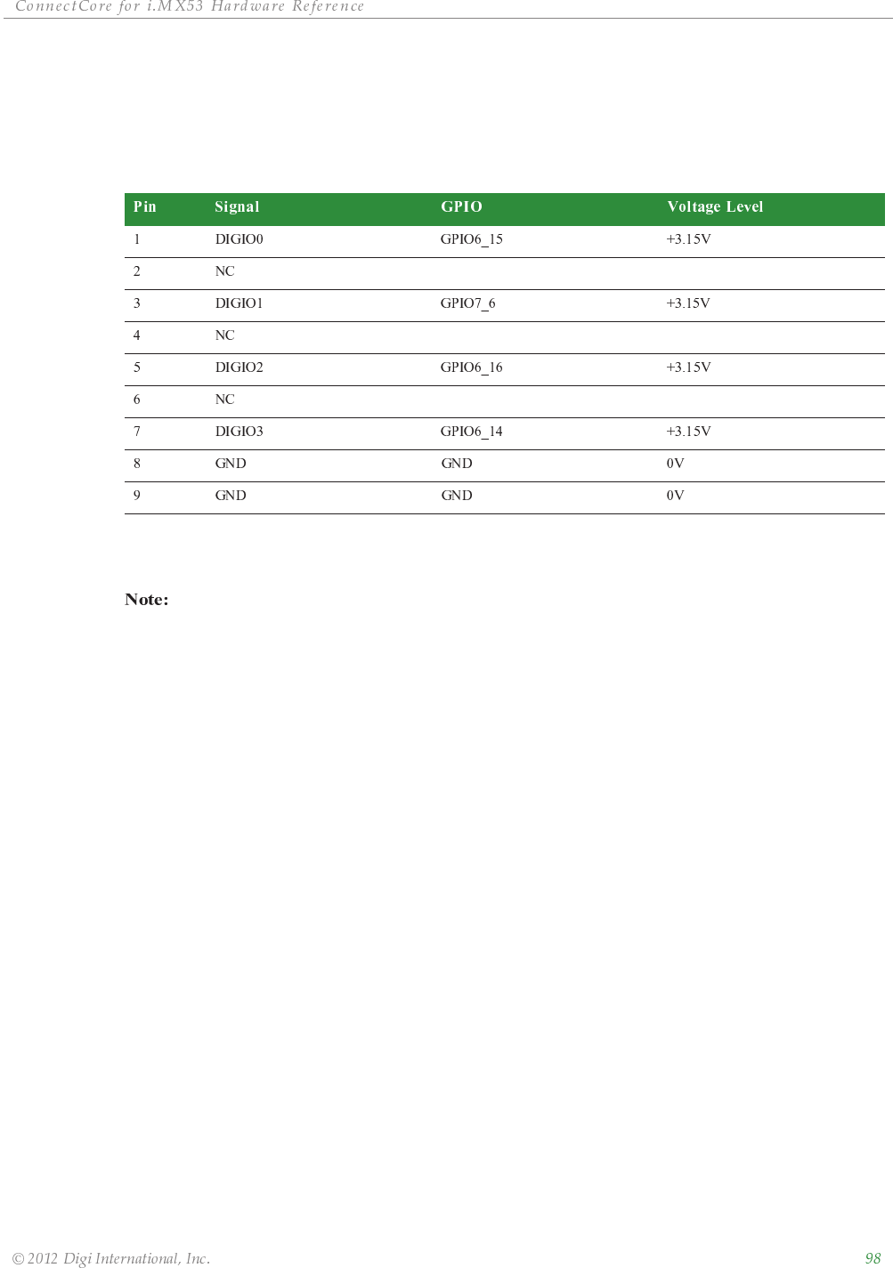
ȱ ȱ ȱ ȱ ȱ ȱ
ȱ ȱ ȱ ȱ ȱȱȱ
Digital I/O Connector, X45
The development board provides a 2x5 position pin header, X45, to access four on-chip digital
GPIOs of the i.MX53 CPU.
On the development board, GPIO6_15, GPIO6_16 and GPIO7_6 are connected to the XBee
interface. When using these signals as digital I/O, the XBee interface should not be used.
The digital I/O interface is not-protected against ESD, over-voltage or inverse polarity.
Care must be taken when using these signals.
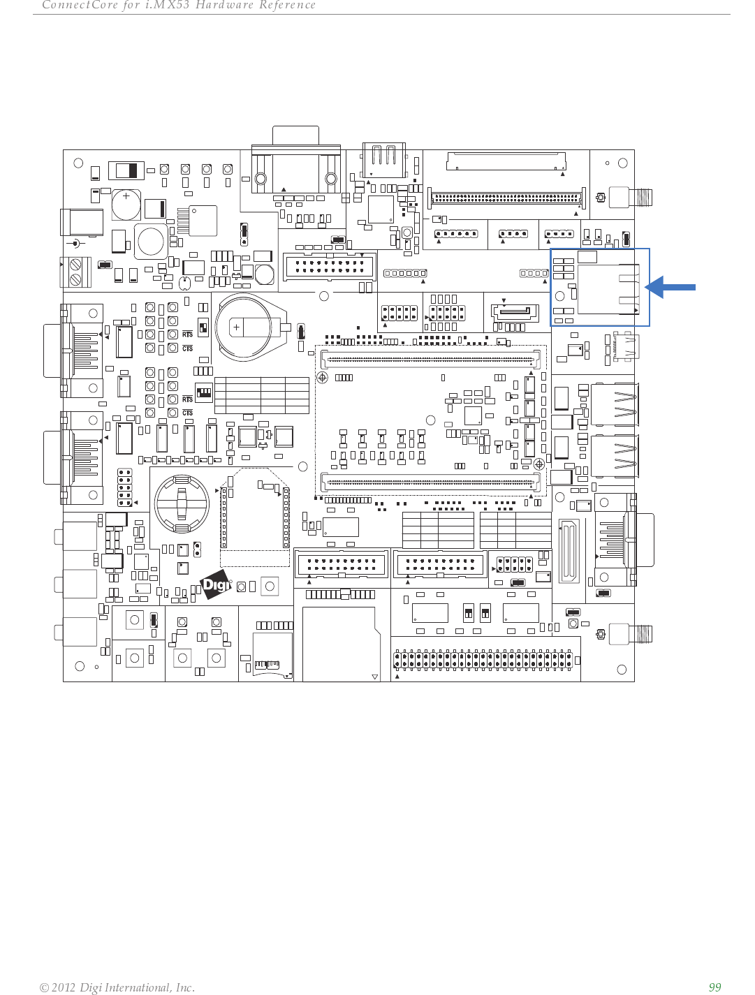
ȱ ȱ ȱ ȱ ȱ ȱ
ȱ ȱ ȱ ȱ ȱȱȱ
Ethernet 1 Interface
The development board provides one 8-wire RJ-45 jack with integrated 1:1 transformers and
link/activity LEDs for the Ethernet 1 interface. This interface is attached to the Fast Ethernet
controller (FEC) of the i.MX53. The ConnectCore for Wi-i.MX53 module provides a 10/100
Ethernet PHY chip for this interface.
The Ethernet 1 RJ-45 connector also supports 802.3af (PoE) operation (optional Digi PoE
application kit required).
R
U3
U50
ON
41 32
S6
ON
1 2
S7
ON
1 2
S8
ON
1 2
S9
S5
S3
S13
S10
H9
H3
D1
U21
U11
Q2
U8 U33
U32
X18
P24 P22 P23
P29
X24
J1
J2
P1
P21
X19
X21
X45 X20
J24
J13
J17
J6
J20
J7
J9
U13
U52 U53
U51 U54
U7
U55
U56
U29
U28
U61
U19
U24
U38
U43
U42
U41
U4
U20U22
U17
U36
U18
U26
U6
U2
U15
JP6
JP20
JP1
JP3
JP10
JP4
JP12
JP5
J19
X32
X29
X28
X7
P20
J11
P19
R139
J27
J10
J8
L8
L26
L27
L21
L19
L22
L20
L25
L24
L18
L28
L29
L9
L12
L16
L3
L4
D5
V5 V6
D6
P12
P13
S12
V2
X30
X27
X31
X14
X16 X15
X13
U46
U10
U35U31U14 U40
LE59LE62LE63 LE61 LE41
LE57
LE60
LE58
LE7 LE6LE4LE8
LE51
LE49
LE40
LE43
LE42
LE44
LE47
LE48
LE45
LE46
LE12
LE50
J23
P14
P15
J15
J12
J18
V10
V11
O1 O2
R130
R131
R51
R133
R134
R28
R228
R56
R71
R75
R77
R74 R55R73
R59
R72
R57
R194
R96
R70
R18
R132
R14
R106
R108
R107
R105
R15
R11
+
C60
+
R52
R84
R41
C2
C1
P2
R45
R49
+
C3
+
R187
R189
R138
R159
R188
R5
R6
R7
C88
C87
C145
C86
R16
R42
R31
R39
R33
RN2
C85
R127
R8
R9
R36 R37
R34
R38
R35
R95
R89
R88
U37
U12
U16
U45
S2
C25
P4
C104
+
C49
C129
R53
C127
C48 C45
R182
C7 C6
L10
L6
L7
L5
R142
R86
+
C109
+
+
C108
+
+
C110
+
+
C111
+
C105
+
+
C90
+
R20
R181
R176
R12 R13
R85
R94
R195
R102
R101
C81
C103
C120
C169
C43
C53
C39
C27
C159
C161
C106
C46
C28
C162
C57
C155
R222
C163
C113 C114 C115
C126
C101
C125 C102
C69
C100
C95
C94
C59
C51
C56
C41
C26
C18
C50
C38
C83
C55
C58
C44
C89
C171
C78
C166
C165
C177
C84
C170
C52
C196
C118
C17
C123
C187
C98
C167
C117
C119
C79
C121
C188C191
C179
R50
C99
C194
C97
C122
C189
C195
C158
C193
C186
C124
C96
C197
C80
C91
C93
C178
R199
C148
C147
C116
C107
C190
C192
C168
C112
R30
R17
R93
R27 R29
R135
R122
R10
U9
+
C20
+
R246
R247
C150
Y1
C153
C22
L23
R143
Y3
C151
C164
R23
C132
C134
C160
C131
C176
C175
C154
C174
C135
C133
C149
C70
C13
C12
C47
C61
C11
C71
C10
C62
C66
R118
R172
R4
R123
R61
R62
R63
R90
C23
R48
R117
R64
R76
R78
R141
R66
R79
R121
R65
R92
R91
R217
R21
R221
R100
R211
R110
R103
R99
R113
R2
R111
R126
R119
R25
R184
R104
R112
R1
R116
R220
R254
R154
R153
C157
C54
R137
L17
J5
U48
U47
U39
U34
U44
U25
U1 U23
U27
U5
R231
R204
R205
R218
R208
R289
R275
R274
R278
R287
R273
R261
R269
R206
R253
R202
R281
R203
R285
R290
R277
R284
R266
R257
R280
R282
R258
R259
R260
R276
R268
R22 R26
R19
R286
R283
R201
R262
R263
C128
R256
R265
R264
R207
R271
R158
R288
R272
R279
R291
R177
R213
R175
R179
R43
R178
R140
R209
R180
R232
R44
R47
R98
R58
R83
R24
R46
R270
R40
R174
R87
R109
R114
R3
R97
R129
R82
R124
R125
R152
R68
R151
R191
R227
R32
R193
R190
R196
R136
R230
R183
R192
R128
R120
R198
R229
R197
R162
C82
C37
C35
C15
C65 C67 C68
C36
C4
C5
C42
C29
C32
C34
C33
C64
C31
C156
C9
C63
C19
C30
C8
C14
C172
R81
R80
R186
R185
R67
R216
C152
C130
L11
L1
U57
LBL1
J4
R173
R214
C24
JP2
R292
C16
R69
R60
L30
R215
R171
U49
C21
U30
J3
C72
H1
R255
R293
U58
R54 C40
TP83TP85
TP61
TP90
TP114
TP67
TP66
TP115
TP69
TP116
TP71
TP117
TP74
TP78TP80
TP63
TP118
TP64
TP22
TP21
TP20
TP19
TP46
TP72
TP45
TP60
TP43
TP84
TP42
TP79
TP65
TP73
TP113
TP137
TP70
TP23
TP24TP81
TP47
TP48
TP77
TP76
TP75
TP93
TP38
TP49
TP52
TP51
TP39
TP41
TP25
TP82
TP89
TP87
TP62
TP29
TP30
TP31
TP28
TP91
TP33
TP35
TP57
TP26
TP37
TP88
TP86
TP68
TP58
TP36
TP92
TP27
TP44
X14
J17 P15
S8
CAN2
SATA
PWM
ON=
WLAN DISABLE
J19
J12
POWER
X27
ON=
P29
S9
S9
S5
_I2C
X21
CLOSE
RXD
J1
+3.3V_JS
SER DOWNLOAD
J18
+3.3V_MOD
DIGI
JTAG
S8
IDENT
DISABLED
USER
P22
+
LINE OUT
UART3 (TTL)
AUTO PWR DWN
J13
+
VCHRG
ON/CLOSE
P4
RESERVED
CAN1 TERMINATION
TXD
CLOSE
UART1 STATUS
X30
OPEN
P12
UART2 (MEI)
LE51
ETHERNET 1
SD/MMC
OPEN
X20
9V-30VDC
SPI
3
LE49
X15
RS485 MODE
+5V
DESCRIPTION
VBATT
J8
1
DISABLED
J10
MAIN POWER
OPEN
P24
J11
LE8
BOOT - SATA
ACTIVE
POS 1
OPEN
4
BUTTON 1
2-WIRE
S6
LVDS
LCD
OFF/OPEN
4-WIRE
ACTIVE
X32
POS
INT. BOOT
VGA
DESCRIPTION
2
MICRO SD
X28
WLAN PRIMARY
J27
ON=ENABLE
COIN CELL
X45
MICRO
1-WIRE
J15
INTERNATIONAL
ETHERNET 2
LE50
CAN1
WLAN SECONDARY
POS 2
J9
P1
OPEN
X29
J24
LED 2
LE4
X18
S13
PARALLEL LCD
S3
S12
XBEE MODULE
OFF
P2
J2
ON=AUTOBOOT
J20
i.MX53 MODULE
POS 1
J7
CLOSE OPEN
RXD
CLOSE
UART2 STATUS
BOOT - FUSES
X16
RESET
TERMINATION
P14
LINE IN
HDMI
X19
CLOSE
ASSOC
CLOSE CLOSE
BOOT - FLASH
POS 2
LED 1
CAN2 TERMINATION
S7
OPEN
X7
BOOT - uSD
BOOT - SD
J6
BUTTON 2
J23
P23
S2
LE6LE7
S10
KEYPAD
MODE
CAMERA 2
RS232
CONNECTCORE
RS422/485
EXT BATT
ENABLE EXT BATT
X24
TOUCH SELECTION
DESCRIPTION
ON
UART1 (CONSOLE)
+3.3VPOWER
LE12
CLOSE
DIGITAL I/O
TXD
PERIPHERAL CONNECTOR
CAMERA 1
BOOT CONF
USB OTG
USB HOST
ON=SJC-ONLY
AUDIO
J3
POE MODULE
P19
POE MODULE
BATT
OPEN
P20
P13
Ethernet 1
RJ-45,
X7
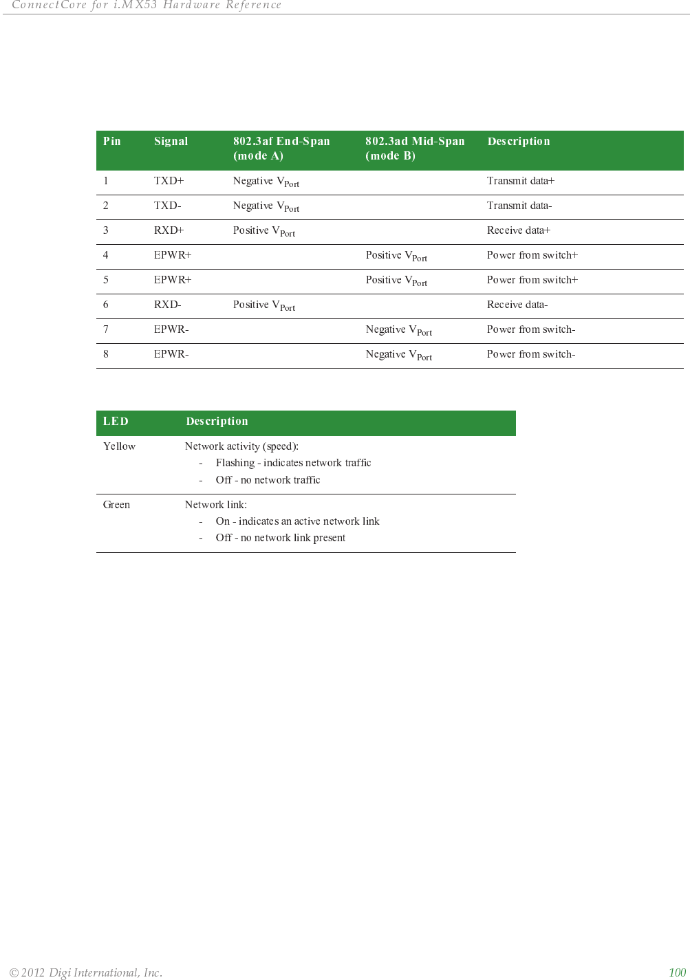
ȱ ȱ ȱ ȱ ȱ ȱ
ȱ ȱ ȱ ȱ ȱȱȱ
Ethernet 1, RJ-45 Connector X7
The table below shows the pinout of the Ethernet 1 RJ-45 connector.
The table below shows the description of the Ethernet 1 LEDs.