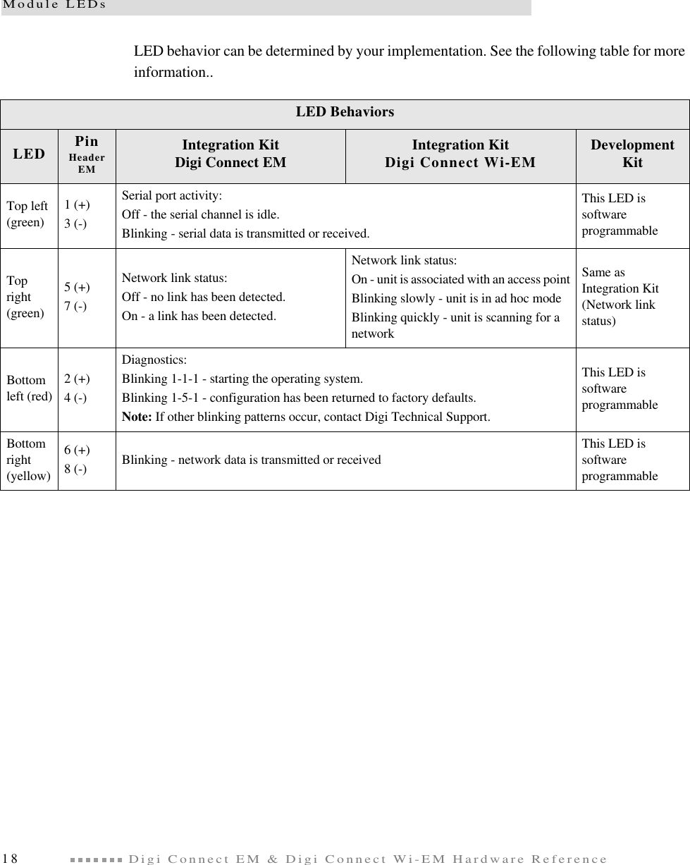
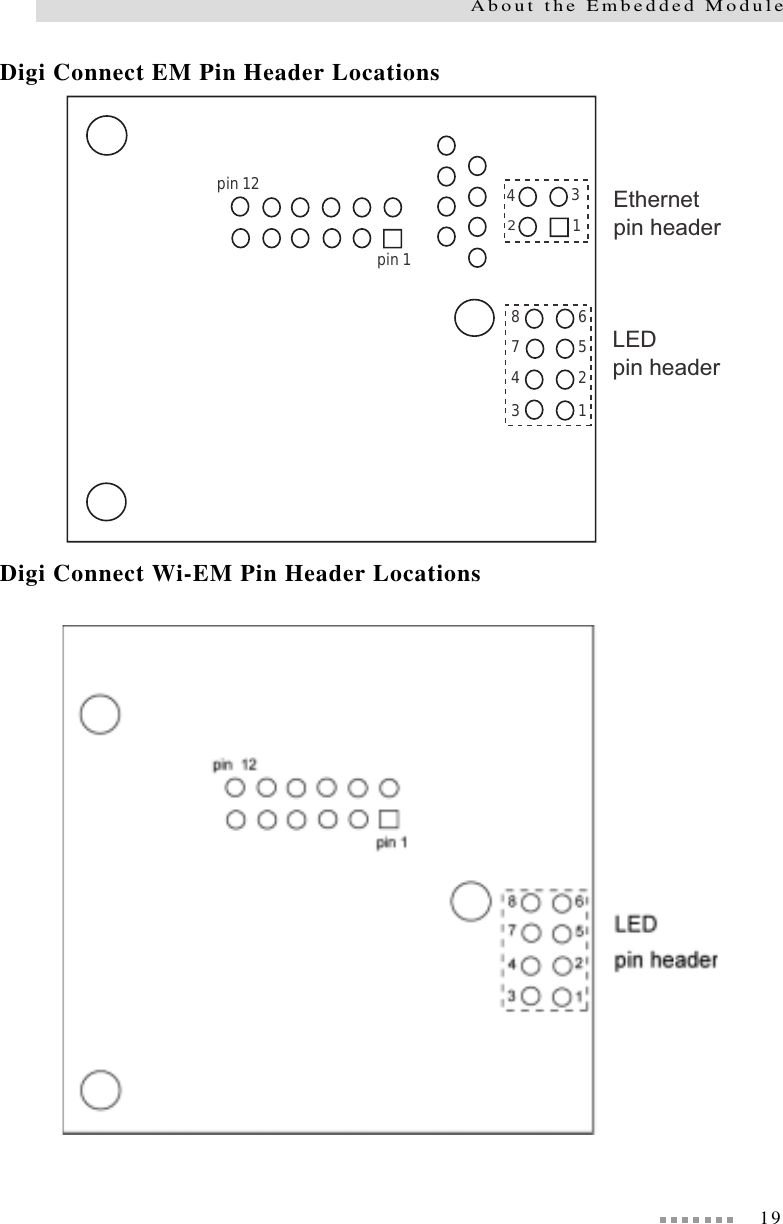
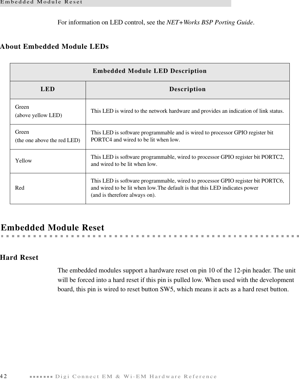
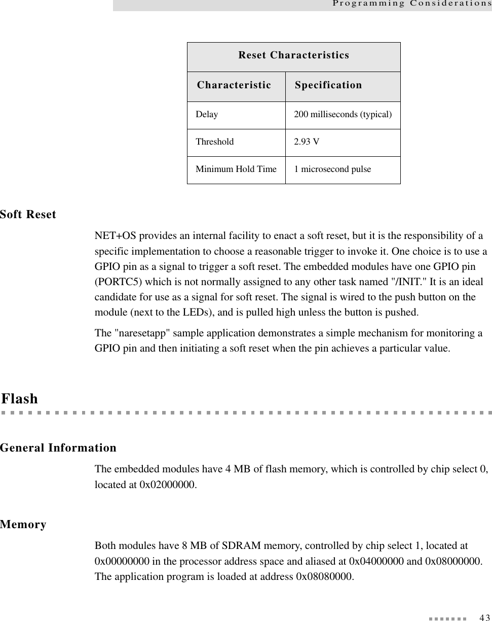
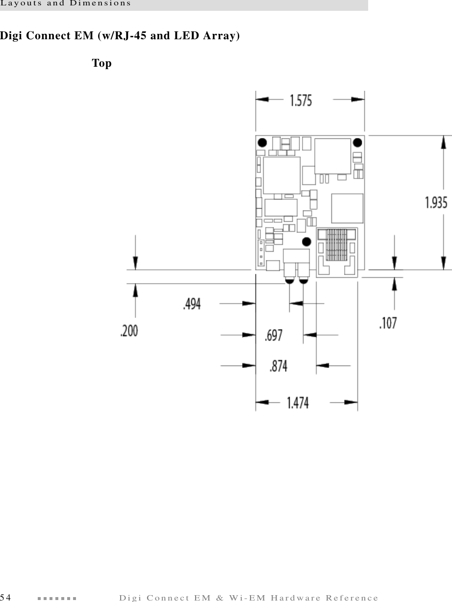
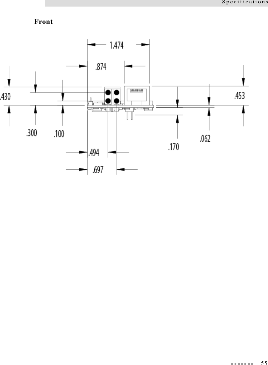
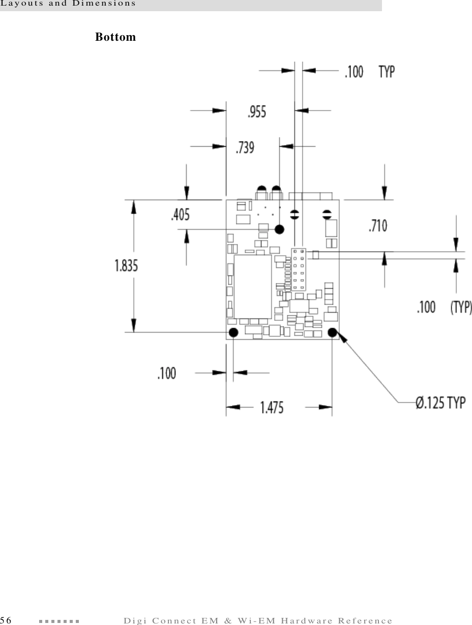
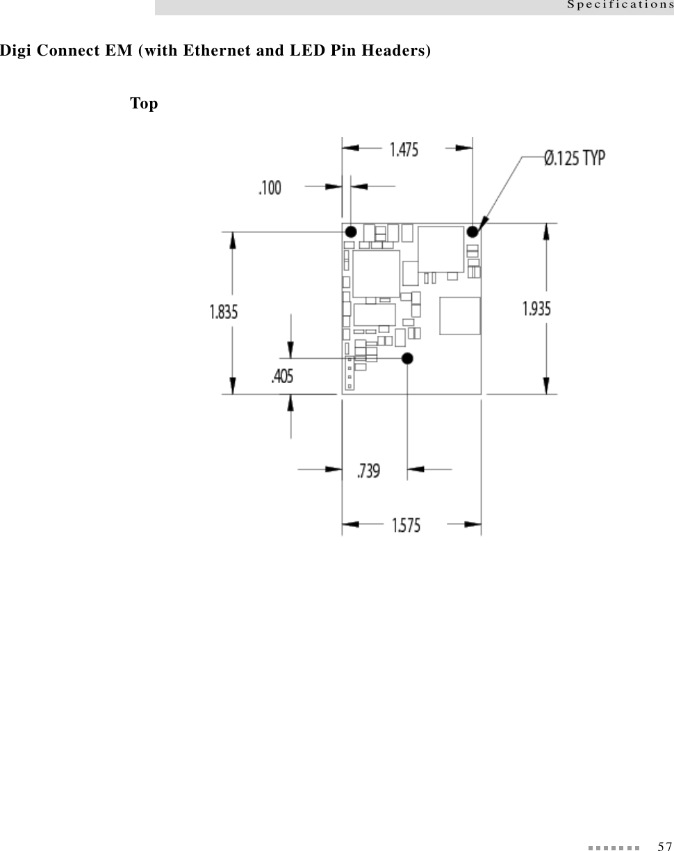
Digi 50M879 802.11b Wireless Module User Manual Digi Connect EM Wi EM Hardware Reference

Digi International Inc 802.11b Wireless Module Digi Connect EM Wi EM Hardware Reference

manual

      TMTM90000632_B
3ContentsAbout This Guide .....................................................................................................................5Scope of Reference Manual .............................................................................................5Kits Contents....................................................................................................................5Related Documentation....................................................................................................7Support Information .........................................................................................................7Chapter 1: About the Embedded Module............................................................................9Overview ..........................................................................................................................9Support Information .......................................................................................................10Types of Modules...........................................................................................................11Connectors: Power and Serial Interface......................................................................... 14Connectors: Ethernet Interface.......................................................................................15Connectors: Antenna ......................................................................................................16Reset Switch................................................................................................................... 17Module LEDs .................................................................................................................17Chapter 2: About the Development Board ........................................................................21Overview ........................................................................................................................21Basic Description ...........................................................................................................21Ports................................................................................................................................ 22Connectors and Blocks...................................................................................................25Power Jack (P17)............................................................................................................29Switches..........................................................................................................................30Development Board LEDs ............................................................................................. 32Test Points......................................................................................................................34Chapter 3: Programming Considerations..........................................................................37
4 GPIO .............................................................................................................................. 37Embedded Module LEDs............................................................................................... 41Embedded Module Reset ............................................................................................... 42Flash............................................................................................................................... 43Appendix A: Specifications .................................................................................................  45Network Interfaces......................................................................................................... 45Serial Interface............................................................................................................... 46Data Rates (bps)............................................................................................................. 46Flow Control Options..................................................................................................... 46Environmental................................................................................................................ 46DC Characteristics ......................................................................................................... 46Mechanical .................................................................................................................... 48Layouts and Dimensions................................................................................................ 48Recommended PCB Layouts ......................................................................................... 59Antenna Information...................................................................................................... 63RF Exposure Statement.................................................................................................. 64Safety Statements........................................................................................................... 65Appendix B: Certifications .................................................................................................  67FCC Part 15 Class B ...................................................................................................... 67Industry Canada ............................................................................................................. 68Declaration of Conformity............................................................................................. 69International EMC Standards......................................................................................... 70Safety Standards............................................................................................................. 70Appendix C: Sample Application: TTL Signals to EIA-232............................................  71
5•••••••••••••••••••••••••••••••••••••••••••••••••••About This GuideScope of Reference ManualThe scope of this guide is to enable developers to integrate the Digi Connect EM or Digi Connect Wi-EM modules into other devices. Graphics illustrate the placement and dimensions of components for both the modules and the development board. Information for both the Digi Connect EM and the Digi Connect Wi-EM are identical unless called out specifically in the manual.Kits ContentsThis manual is intended for customers who use either the Digi Connect EM/Digi Connect Wi-EM Integration Kit or the Digi Connect EM/Digi Connect Wi-EM Development Kit, which are described below. About the Integration KitThe integration kit is the ideal platform for product evaluation, rapid prototyping, and integration of the Digi Connect EM or Digi Connect Wi-EM embedded device server. Targeted specifically at customers who want to take advantage of the Digi Connect EM or Digi Connect Wi-EM embedded device server with Digi plug-and-play firmware functionality, both products enable integration of the Digi Connect EM or Digi Connect Wi-EM embedded module without any extensive embedded software development with all the additional flexibility and benefits of web user interface customization and application specific java applets. Included in the Digi Connect EM or Digi Connect Wi-EM Integration Kits are the following:
Kits Contents6Digi Connect EM & Wi-EM Hardware ReferenceComplete development board with EIA-232 serial ports, signal status indicators, logic analyzer connectors, test points, and a self-contained GPIO test bed. Cables– DB-9 to DB-9 Crossover cable– DB-9 to DB-9 Modem cable– RJ-45 Ethernet Crossover cableLoopback plugPower supplyWrist strap (for grounding)Digi Connect CD– sample code– tools and utilities with source code and libraries – Microsoft Windows RealPort drivers Full software and hardware documentationAbout the Development KitThe Digi Connect EM or Digi Connect Wi-EM Development Kit is an easy-to-use and royalty-free development platform that significantly reduces traditional design risk and accelerates the overall software development process. Both kits deliver the integrated building blocks to quickly and cost effectively create your own custom firmware for a Digi Connect EM or Digi Connect Wi-EM based high-performance networking solution that fits the specific requirements of your application.Based on the NET+Works family of platform solutions, the Digi Connect EM or Digi Connect Wi-EM development kits enable you to integrate custom network connectivity into your products quickly by providing a full suite of development tools inlcuding: Development board CablesPower supply
7Hardware debugger Complete set of networking protocols and applications softwareRelated DocumentationSee the NS 7520 Hardware Reference for information on the NS 7520 chip.Support InformationTo get help with a question or technical problem or make comments and recommendations about Digi products and documentation, use the following contact information.General  Customer Service and SupportDigi International11001 Bren Road EastMinnetonka, MN 55343U.S.A.United States: 1 877-912-3444Other Locations: 1 952-912-3444support.digi.comwww.digi.com
Support Information8Digi Connect EM & Wi-EM Hardware Reference
9About the Embedded ModuleCHAPTER 1OverviewDigi Connect EM and Digi Connect Wi-EM OverviewThe embedded modules are part of the Digi Connect family of device servers that provide simple, reliable and cost-effective network connections for serial devices. They provide fully transparent serial device connectivity over industry-standard Ethernet connections and allow both equipment manufacturers and systems integrators to network-enable products at a fraction of the time and cost required to develop a custom solution. It is a highly flexible and compact single component solution with a robust on-board TCP/IP stack and 10/100 Base-T Ethernet or wireless support. Features include the following:32-bit NS7520 processor with ARM7TDMI core4MB Flash and 8MB RAM on board2 High Speed Serial Ports9 Mbps SPI Master Mode Interface9 General Purpose Input/Output Port OptionsAvailable with Digi plug-and-play firmwareNetSilicon NET+Works platform for embedded software development
Support Information10Digi Connect EM & Digi Connect Wi-EM Hardware ReferenceFrom medical systems to building control and industrial automation, in virtually any application where embedded serial connectivity over Ethernet is needed, the embedded module is the ideal choice, delivering high-performance functionality.CautionsTo guard against damage to the module due to electrostatic discharge (ESD), do not remove it from its protective packaging until you have been properly grounded. To ground yourself, put the wrist strap on (included in the package) and then attach the clip to a metal surface. Input voltage for the module is 3.3 VDC.Support InformationTo get help with a question or technical problem or make comments and recommendations about Digi products and documentation, use the following contact information.General Digi International11001 Bren Road EastMinnetonka, MN 55343U.S.A.www.digi.comCustomer Service and SupportUnited States: 1 877-912-3444Other Locations: +1 952-912-3444www.digi.com/support
11About the Embedded ModuleTypes of ModulesThe following describes the three types of Digi Connect EM and three types of Digi Connect Wi-EM modules:Choosing a Module for Your ProductAlthough any of the embedded modules can be designed into your product, a JTAG header would typically be used only for debugging during the development process. The Digi Connect EM module part number DC-EM-02T-S or DC-EM-02T-C is appropriate when its integrated LEDs and RJ-45 Ethernet connectors are accessible and visible to the end-users of your product. The Digi Connect EM module part number DC-EM-02T-NC or DC-EM-02T-JT is the right choice when you want more control over RJ-45 Ethernet connector and LED locations or when you will provide custom connectors or indicators.The Digi Connect Wi-EM module part number DC-WEM-02T-C or DC-WEM-02T-S is appropriate when its integrated LEDs are accessible and visible to the end-users of your product. The Digi Connect Wi-EM module part number DC-WEM-02T-JT or DC-WEM-02T-NC is the right choice when you want more control over LED locations or when you will provide custom connectors or indicators.Please refer to the Digi website www.digi.com for part number and ordering information for the modules
Types of Modules12Digi Connect EM & Digi Connect Wi-EM Hardware ReferenceDC-EM-02T-ST.CDigi Connect EM ModulesModel Description FigureDC-EM-02T-JTUsed for development purposes onlyJTAG interfacePin headers for Ethernet and LED functionality.DC-EM-02T-NCNo JTAG interfacePin headers for Ethernet and LED functionalityOrdered independently of development kit for use in your implementationDC-EM-02T-SDC-EM-02T-CNo JTAG interfaceRJ-45 Ethernet connector and LED arrayOrdered independently of either the development or integration kit for use in your implementation. Digi Connect Wi-EM ModulesModel Description FigureDC-WEM-02T-JTUsed for development purposes onlyJTAG interfacePin headers LED functionalityDual RP-SMA Antenna Connector.
13About the Embedded ModuleNote -S: No JTAG, w/ LED array, w/RJ-45/antenna connectors, for use with Digi Firmware-C: No JTAG, w/LED array, RJ-45 / antenna connectors, for use with Custom Firmware-NC: No JTAG, w/LED pin header, w/o RJ-45 connector (for Digi Connect EM), w/antenna connectors (for Digi Connect Wi-EM), for use with custom firmware (not shown)-JT: w/ JTAG, w/pin header, w/o RJ-45 connector (for Digi Connect EM), w/antenna connectors (for Digi Connect Wi-EM), for use with custom firmware developmentDigi Connect Wi-EM AntennaeThe Digi Connect Wi-EM is available with dual-diversity antenna connectors. The right antenna (P2) is always used for transmit and receive.The left antenna is receive only. The antenna will choose the best signal (pin vs. socket). The Digi Connect Wi-EM always has two antenna connectors but using the second antenna is optional.The antennae are connected to the module with reverse polarity SMA connectors (sub-miniature size A). The antennae fit the connectors on the module only one way to ensure a proper connection. The antennae function best when placed perpendicular to each other (one straight, the other up or down) to prevent interference from each other. DC-WEM-02T-NCNo JTAG interfacePin headers LED functionalityDual RP-SMA Antenna ConnectorOrdered independently of development kit for use in your implementationDC-WEM-02T-CDC-WEM-02T-SNo JTAG interfaceLED arrayDual RP-SMA Antenna ConnectorOrdered independently of either development or integration kit for use in your implementation. Digi Connect Wi-EM ModulesModel Description Figure
Connectors: Power and Serial Interface14Digi Connect EM & Digi Connect Wi-EM Hardware ReferenceAnother option for both signal reception and design flexibility is to use a "pig tail" cable Digi part number DC-ANT-EC to separate the antenna from the module. This allows the module to fit inside your product but the antenna to be placed outside the device.Connectors: Power and Serial Interface This single 12-pin, serial interface port (labeled P4 for Digi Connect EM and P5 for Digi Connect Wi-EM) supports 2 TTL serial interfaces, data rates up to 230 Kbps and full-modem control (on port 1). See the figure for help locating pins and the table for pin assignments.Power and Serial InterfacePower and Serial Interface Pin AssignmentsPin  Signal Name Description and Notes1 VCC +3.3 VDC (input only)2 GND Reference Ground for input power3 RXD/GPIO-7 Port 1 RXD (input)/GPIO-74 TXD/GPIO-6 Port 1 TXD (output)/GPIO-65 RTS/GPIO-4/SPI_CLK Port 1 RTS/GPIO-4/SPI clockGRNGRNREDYELPIN1PIN1pin 1 234567891011 12
15About the Embedded ModuleConnectors: Ethernet Interface The following table shows the pinout of the RJ-45 connector..For a diagram of the Digi Connect Ethernet pin header location and assignments see "Digi Connect EM Pin Header Locations" on page 19.6 DTR/GPIO-5 Port 1 DTR (output)/GPIO-57 CTS/GPIO-2 Port 1 CTS (input)/GPIO-28 DCD/GPIO-1/SPI_EN Port 1 DCD (input)/GPIO-1/SPI enable9 DSR/GPIO-3 Port 1 DSR (input)/GPIO-310 /RST Reset (input)11 RXD/GPIO-9 Port 2 RXD (input)/GPIO-912 TXD/GPIO-8 Port 2 TXD (output)/GPIO-8Power and Serial Interface Pin AssignmentsPin  Signal Name Description and NotesRJ-45 Ethernet InterfacePin # 1 2 3 4 5 6 7 8Signal TXD+ (Transmit Data)TXD- (Transmit Data)RXD+ (Receive Data)Not used Not usedRXD- (Receive Data)Not used Not used
Connectors: Antenna16Digi Connect EM & Digi Connect Wi-EM Hardware ReferenceConnectors: AntennaThe Digi Connect Wi-EM has 2 RP-SMA antenna connectors labeled P2 and P3.Wi-EM Antenna ConnectorsAntenna SpecificationsType DipolePart number   DC-ANT-24DPGain   2 dBiCaution: This Part 15 radio device operates on a non-interference basis with other devices operating at this frequency when using the antennaelisted in the Antenna Specification table. Any changes or modification touser’s authority to operate the device.the product not expressly approved by Digi International could void the
17About the Embedded ModuleReset SwitchThe behavior of the reset switch is determined by software, which means that it has a predefined behavior in the integration kit. In the development kit, its behavior is determined by your implementation. See the following table for details.Reset Switch LocationNote The reset switch is in same location for both wired and wireless modules.Module LEDsThe modules provide two hardware options for LEDs, with or without on board LED array. The integration kit provides predefined LED behavior. With the development kit, some Reset Switch BehaviorKit BehaviorIntegration The reset switch does one of the following:If pressed and released immediately, the device is rebooted.If pressed and held down (for about 20 seconds) during power-up, the device is rebooted and restored to the default configuration.Development The behavior of the switch is user-defined.See "Embedded Module Reset" on page 42 for more information.
Module LEDs18Digi Connect EM & Digi Connect Wi-EM Hardware ReferenceLED behavior can be determined by your implementation. See the following table for more information..LED BehaviorsLED PinHeaderEMIntegration KitDigi Connect EM Integration KitDigi Connect Wi-EM DevelopmentKitTop left(green)1 (+)3 (-)Serial port activity: Off - the serial channel is idle. Blinking - serial data is transmitted or received.This LED is softwareprogrammableTop right(green)5 (+)7 (-)Network link status:Off - no link has been detected.On - a link has been detected.Network link status:On - unit is associated with an access pointBlinking slowly - unit is in ad hoc modeBlinking quickly - unit is scanning for a networkSame as Integration Kit(Network link status)Bottomleft (red)2 (+)4 (-)Diagnostics:Blinking 1-1-1 - starting the operating system.Blinking 1-5-1 - configuration has been returned to factory defaults. Note: If other blinking patterns occur, contact Digi Technical Support.This LED is softwareprogrammableBottomright(yellow)6 (+)8 (-) Blinking - network data is transmitted or receivedThis LED issoftwareprogrammable
19About the Embedded ModuleDigi Connect EM Pin Header LocationsDigi Connect Wi-EM Pin Header Locations411256347823pin 12pin 1Ethernetpin headerLEDpin header
Module LEDs20Digi Connect EM & Digi Connect Wi-EM Hardware Reference
21About the Development BoardCHAPTER 2OverviewThis chapter provides information on the development board, a hardware platform from which you can determine how to integrate the embedded module into your design. For additional information, see the schematic and mechanical drawings. If you have installed the development kit or integration kit, you can access the schematic from the Start menu.Basic DescriptionThe development board can be used by both module feature sets with the Integration Kit or the Development Kit.The following graphic is a layout of the development board.
Ports22Digi Connect EM & Wi-EM Hardware ReferenceBasic DescriptionPortsThe development board provides the following ports:Serial Port 1 (P1) and Serial Port 2 (P2) Ethernet Port (P12)
23About the Development BoardGPIO Port (P3)Serial Port 1 (P1) and Serial Port 2 (P2)Serial port 1 and port 2 are DB-9 male connectors labeled P1 and P2. Use the following figure and table for pin orientation and pin assignment information.Serial Port Pin Orientation00000006Pin 1 Pin 5Pin 6 Pin 9Serial Pin AssignmentPort  SignalPin 1 SignalPin 2 SignalPin 3 SignalPin 4 SignalPin 5 SignalPin 6 SignalPin 7 SignalPin 8 SignalPin 91DCD RXD TXD DTR GND DSR RTS CTS NotConnected2NotConnected RXD TXD NotConnected GND NotConnectedNotConnectedNotConnectedNotConnected
Ports24Digi Connect EM & Wi-EM Hardware ReferenceEthernet Port (P12)The Ethernet port of the Digi Connect EM embedded module (labeled P12) is an 8-pin RJ-45 jack meeting the requirements of ISO 8877 for 10/100Base-T. When two descriptions are shown for a pin, the second is for use with 802.3af powered Ethernet.For additional information about the 802.3af standard, refer to the corresponding IEEE specification.Note The development board provides a reference design of a POE (Power Over Ethernet) power supply. A schematic for this reference design is installed by the setup program on the CD.GPIO Port (P3)The GPIO port is a 10-pin male right-angle connector (labeled P3). See the following figure and table for pin orientation and pin assignments. GPIO Port Pin OrientationEthernet Pin AssignmentsPin Signal Name FigureRJ-45 (P12)1 TXD+ (Transmit Data)2 TXD- (Transmit Data)3 RXD+ (Receive Data)4 Not used / power (+)5 Not used / power (+)6 RXD- (Receive Data)7 Not used / power (-)8 Not used / power (-)Pin1Pin 1 Pin 1000000020
25About the Development BoardConnectors and BlocksThe development board provides the following connectors and blocks:JTAG Debugger Connector (P4)SPI Connector (P11) and SPI Jumper BlockLogic Signal Analyzer Header (P6)Main Connector (P8)JTAG Debugger Connector (P4) This 14-pin male vertical header labeled P4 mates with a JTAG debugger plug (for example, a Macraigor Raven). It is used with the development kit only. See the following figure and table for pin orientation and assignments.GPIO Port Pin AssignmentsPin Signal Name1GND2GPIO-93GPIO-84GPIO-75GPIO-66GPIO-57GPIO-48GPIO-39GPIO-210 GPIO-1
Connectors and Blocks26Digi Connect EM & Wi-EM Hardware ReferenceJTAG Debugger Connector Pin OrientationSPI Connector (P11)This connector is used for a Serial Peripheral Interface (SPI) connection. When enabled, signals are disconnected from serial port 1 and GPIO connectors. See the following figure and table for pin orientation and pin assignments.SPI Connector Pin Orientationpin121314JTAG Debugger Connector Pin AssignmentsPin 1Pin 2Pin3Pin4Pin 5Pin6Pin7Pin8Pin9Pin10 Pin11 Pin12 Pin13 Pin14Signal VCC+ GND /TRST GND TDI GND TMS GND TCK GND TDO /SRST VCC+ GNDPin 1Pin 2Pin 7Pin 8
27About the Development BoardSPI Jumper BlockThe SPI jumper block determines whether the SPI connector is connected or not. If SPI is off (the default), serial and GPIO signals are routed to switch banks 1 through 4. (See "Serial/GPIO Switch Bank 3 (SW3) and Switch Bank 4 (SW4)" on page 31 and "GPIO Switch Bank 1 (SW1) and 2 (SW2)" on page 32.) If SPI is on, SPI signals are routed to the SPI connector (P11).The following figures demonstrate how to set the SPI jumper blockSPI Jumper SettingsLogic Signal Analyzer Header (P6)This 20-pin male vertical header (labeled P6) connects a digital signal analyzer (for example, a logic analyzer) to the development board. It is used with the development kit only. See the following figure and table for pin orientation and pin assignments.SPI Pin AssignmentsPin1Pin 2Pin 3Pin 4Pin5Pin 6Pin7Pin 8Pin 9Pin 10Signal SPI-EN GND SPI-CLK GND SPI-TX GND SPI-RX GND Not connectedNotconnectedSPI OFF SPI ONoo
Connectors and Blocks28Digi Connect EM & Wi-EM Hardware ReferenceLogic Analyzer Header Pin OrientationLogic Analyzer Header Pin AssignmentsPin  Signal1 - 8 Not connected9/RST10 Not connected11 DTR/GPIO-512 TXD-2/GPIO-813 CTS/GPIO-214 RXD-2/GPIO-915 DSR/GPIO-316 TXD-1/GPIO-617 RTS/GPIO-4/SPI_CLK 18 RXD-1/GPIO-719 DCD/GPIO-1/SPI_EN20 GNDPin 2Pin 20Pin 1Pin 19
29About the Development BoardMain Connector (P8)This 12-pin connector is used to interface with the embedded module. See the following figure for pin orientation.Main Connector Pin OrientationPower Jack (P17)The Power Jack is a barrel connector that accepts 9 to 30 VDC +/- 5%. The jack is labeled P17. The following table shows the polarity of the power jack.Pin 1 Pin 11Pin 2 Pin 12Power Jack PolarityContact PolarityCenter +9 to +30 VDCOuter Ground
Switches30Digi Connect EM & Wi-EM Hardware ReferenceThe following figure schematically represents the polarity of the power jackPower Jack Polarity Schematic.SwitchesThe development board provides the following switches:Reset Switch (SW5) Serial/GPIO Switch Bank 3 (SW3) and Switch Bank 4 (SW4)GPIO Switch Bank 1 (SW1) and 2 (SW2)Reset Switch (SW5)This push button switch is labeled SW5. Pressing it sets the module’s /RST line low, holding the module in a hard reset until the switch is released.Note: This is a "hard" reset using the /RST pin on the main connector, not a "soft" reset. The reset button on the embedded module performs a "soft" reset (see also "Main Connector (P8)" on page 29). Ground +9 to +30  VDC
31About the Development BoardSerial/GPIO Switch Bank 3 (SW3) and Switch Bank 4 (SW4)Each switch bank holds five slide switches that enable either serial or GPIO signaling between the development board and the module. When set for GPIO signaling, SW3 works in conjunction with SW1, and SW4 works with SW2. See "GPIO Switch Bank 1 (SW1) and 2 (SW2)" on page 32 for more information. See the following table for SW3 and SW4 switch definitions.Note: These switches control where the development board routes a signal. They do not reconfigure the NS7520 processor. Software should be configured to track with switch settings. See "GPIO" on page 37 for more information. GPIO Switch Banks 3 and 4 SettingsSwitch Bank Switch Number LeftPosition RightPositionSW31DCDGPIO-12CTSGPIO-23DSRGPIO-34RTSGPIO-45DTRGPIO-5SW46 TXD-1 GPIO-67 RXD-1 GPIO-78 TXD-2 GPIO-89 RXD-2 GPIO-910 Not connected Not connected
Development Board LEDs32Digi Connect EM & Wi-EM Hardware ReferenceGPIO Switch Bank 1 (SW1) and 2 (SW2)GPIO Switch Bank 1 and Switch Bank 2, labeled SW1 and SW2, are two sets of five slide switches that set GPIO inputs to logic levels of high (switch to left) or low (switch to right). If the GPIO port is configured as an output, then the switch should always be to the left. If there is an external device connected to P3, the switch should always be set to the left.Each GPIO port can be used independently.Notes:These switches do not determine whether the GPIO is an input or output. That is determined by the module software. If GPIO is set to an output by software, switches must be set to the left (high). These switches are used in conjunction with SW3 and SW4.Development Board LEDsThe development board contains 21 LEDs labeled CR1 through CR21. The following table lists and describes the LEDs.LED DescriptionsBoardLabel  DescriptionColor or StateIndicationCR1 TXD-2 Flickering Serial activityGreen Inactive CR2 RXD-2 Flickering Serial activityGreen Inactive CR3 CTSYellow ActiveGreen Inactive Off Not connected or signal not being driven
33About the Development BoardCR4 DTRYellow Active Green Inactive Off Not connected or signal not being drivenCR5 TXD-1 Flickering Serial activityGreen Inactive CR6 RXD-1 Flickering Serial activityGreen InactiveCR7 RTSYellow ActiveGreen InactiveOff Not connected or signal not being drivenCR8 DCDYellow ActiveGreen InactiveOff Not connected or signal not being drivenCR9 DSRYellow ActiveGreen InactiveOff Not connected or signal not being drivenCR10 -18GPIO-1 through GPIO-9. (CR10=GPIO-1, CR11=GPIO-2, etc. All can be used for input or output.)On Logic highOff Logic lowCR20 3.3V Indicator On Power onOff Power offLED DescriptionsBoardLabel  DescriptionColor or StateIndication
Test Points34Digi Connect EM & Wi-EM Hardware ReferenceTest PointsThe development board provides 25 test points that can be identified by board label or test point number. The board labels are adjacent to each test point on the board. The test point numbers are in the development board schematic drawings. The following table lists the test point number, board label, and a brief description of each test point.CR21 EPWR, Powered Ethernet EnabledOnEthernet power present from external powered Ethernet connector (Ethernet hub or switch)Off No powered Ethernet voltageLED DescriptionsBoardLabel  DescriptionColor or StateIndicationTest Point DescriptionsTest Point  Board Label DescriptionTP2 TXD TXD-2TP3 RXD RXD-2TP4 CTS CTSTP5 DTR DTRTP6 TXD TXD-1TP7 RXD RXD-1TP8 RTS RTSTP9 DCD DCDTP10 DSR DSR
35About the Development BoardTP11 IO-1 GPIO-1TP12 IO-2 GPIO-2TP13 IO-3 GPIO-3TP14 IO-4 GPIO-4TP15 IO-5 GPIO-5TP17 3.3V 3.3V SupplyTP20 RESET Reset (active low)TP21 E+ Ethernet Power +TP22 E- Ethernet Power -TP23 V-IN 9-30 VDC InputTP24 GND GroundTP25 GND GroundTP26 IO-8 GPIO-8TP27 IO-7 GPIO-7TP28 IO-6 GPIO-6TP29 IO-9 GPIO-9Test Point DescriptionsTest Point  Board Label Description
Test Points36Digi Connect EM & Wi-EM Hardware Reference
37Programming ConsiderationsCHAPTER 3This chapter addresses the embedded modules programming considerations.Note This chapter applies only to development kit customers. GPIOGeneral InformationThe NS7520 processor supports 16 general purpose I/O (GPIO) lines, some of which are reserved for specific functions and some of which can be customized. These GPIO lines fall into three categories: Those labeled “Reserved” in the following table are reserved for a specific use and must not be reprogrammed, or the unit may not operate correctly. Often, these lines are not connected to external interfaces. Those labeled “Allocated” in the following table are exposed to an external interface and allocated to a specific use by the software, but they can be customized safely with code modifications.Those labeled “Available” are exposed to an external interface, not controlled directly by the software, and can be customized.
GPIO38Digi Connect EM & Wi-EM Hardware ReferenceGPIO RegistersTwo registers, PORTA and PORTC, govern the 16 GPIO pins. Each is responsible for eight GPIO pins, and each pin has four bits that completely describe its behavior. The four bits that describe the GPIO behavior are its mode (CMODE), direction (CDIR), special function (CSF--only applicable to PORTC), and data value. The first three bits describe the functionality of the GPIO pin. The "data" bit provides the current value of the pin when read and allows control of the value of an output pin when written. Use the following table for information on configuring a bit position in the appropriate register for GPIO input or output. Since each register controls 8 GPIO lines, it is safest to read the full 32 bit register, modify the bits corresponding to the GPIO line of interest, and then write the full 32 bits back.  In this way, the behavior of the other GPIO lines will be preserved.For more information regarding the format and programming of the GPIO registers, see the NS7520 Hardware Reference.Configuring a GPIO Pin for Input and OutputInput OutputCMODE = 0 CDIR = 0 CSF = 0CMODE = 0 CDIR = 1 CSF = 0
39Programming ConsiderationsGPIO Pin UseGPIO Pin UseName RegisterBit Category ExternalInterface DescriptionTXD/GPIO-6 PORTA7 Allocated Pin 4 on the main header Used for port 1 serial transmit but can be reassigned as GPIO input or output. If used with the development board, this pin maps to GPIO-6.DTR/GPIO-5 PORTA6 Allocated Pin 6 on the main header Used for the port 1 serial DTR signal but can be reassigned as GPIO input or output. If used with the development board, this pin maps to GPIO-5.See the descriptionPORTA5, PORTA4 Allocated Pin 5 on the main headerSince these two processor pins map to the same header pin, one must be configured as an input to avoid contention. Under normal serial conditions, PORTA5 is configured to deliver the port 1 RTS signal and PORTA4 for GPIO input. To use the port for SPI, configure PORTA5 for GPIO input and PORTA4 to deliver SPI clock. When used with the development board, header pin 5 maps to GPIO-4.RXD/GPIO-7 PORTA3 Allocated Pin 3 on the main headerUsed for port 1 serial receive but can be reassigned as GPIO input or output. If used with the development board, this pin maps to GPIO-7.
GPIO40Digi Connect EM & Wi-EM Hardware ReferenceDSR/GPIO-3 PORTA2 Allocated Pin 9 on the main headerUsed for the port1 serial DSR signal but can be reassigned as GPIO input or output. If used with the development board, this pin maps to GPIO-3.CTS/GPIO-2 PORTA1 Allocated Pin 7 on the main headerUsed for the port 1 serial CTS signal but can be reassigned as GPIO input or output. If used with the development board, this pin maps to GPIO-2.DCD/GPIO-1 PORTA0 Allocated Pin 8 on the main headerUsed for the port 1 serial DCD signal but can be reassigned as GPIO input or output. If used with the development board, this pin maps to GPIO-1.TXD2/GPIO-8 PORTC7 Allocated Pin 12 on the main headerUsed for port 2 serial transmit but can be reassigned as GPIO input or output. If used with the development board, this pin maps to GPIO-8.Power indicator LEDPORTC6 Allocated Connected to the red LEDUsed as the power indicator (always on) but can be reassigned as a general purpose LED. It must remain a GPIO output for the LED to operate correctly. This LED is lit when the signal is low./INIT PORTC5 AvailableConnected to the button on the moduleShould be configured as a GPIO input.GPIO Pin UseName RegisterBit Category ExternalInterface Description
41Programming ConsiderationsEmbedded Module LEDsGeneral informationThe embedded module has two types of LEDs: LEDs connected directly to GPIO pins on the processor and controlled directly in softwareLEDs connected to other hardware components (Ethernet/wireless hardware) and not directly programmable by the operating systemGreen LED PORTC4 AllocatedConnected to the green LED (the one above the red LED)Used as the NET+OS green LED but can be reassigned as a general purpose LED. It must remain a GPIO output for the LED to operate correctly. The LED is lit when the signal is low.RXD2/GPIO-9 PORTC3 Allocated Pin 11 on the main headerUsed for port 2 serial receive but can be reassigned as GPIO input or output. If used with the development board, this pin maps to GPIO-9.Yellow LED PORTC2 AllocatedConnected to the yellow LEDUsed as the NET+OS yellow LED but can be reassigned as a general purpose LED. It must remain a GPIO output for the LED to operate correctly. The LED is lit when the signal is a low.PORTC1- PORTC0 Reserved NA NAGPIO Pin UseName RegisterBit Category ExternalInterface Description
Embedded Module Reset42Digi Connect EM & Wi-EM Hardware ReferenceFor information on LED control, see the NET+Works BSP Porting Guide.About Embedded Module LEDsEmbedded Module Reset Hard ResetThe embedded modules support a hardware reset on pin 10 of the 12-pin header. The unit will be forced into a hard reset if this pin is pulled low. When used with the development board, this pin is wired to reset button SW5, which means it acts as a hard reset button.Embedded Module LED DescriptionLED DescriptionGreen (above yellow LED) This LED is wired to the network hardware and provides an indication of link status.Green(the one above the red LED)This LED is software programmable and is wired to processor GPIO register bit PORTC4 and wired to be lit when low.Yellow This LED is software programmable, wired to processor GPIO register bit PORTC2,and wired to be lit when low.RedThis LED is software programmable, wired to processor GPIO register bit PORTC6,and wired to be lit when low.The default is that this LED indicates power(and is therefore always on).
43Programming ConsiderationsSoft ResetNET+OS provides an internal facility to enact a soft reset, but it is the responsibility of a specific implementation to choose a reasonable trigger to invoke it. One choice is to use a GPIO pin as a signal to trigger a soft reset. The embedded modules have one GPIO pin (PORTC5) which is not normally assigned to any other task named "/INIT." It is an ideal candidate for use as a signal for soft reset. The signal is wired to the push button on the module (next to the LEDs), and is pulled high unless the button is pushed. The "naresetapp" sample application demonstrates a simple mechanism for monitoring a GPIO pin and then initiating a soft reset when the pin achieves a particular value.FlashGeneral InformationThe embedded modules have 4 MB of flash memory, which is controlled by chip select 0, located at 0x02000000.MemoryBoth modules have 8 MB of SDRAM memory, controlled by chip select 1, located at 0x00000000 in the processor address space and aliased at 0x04000000 and 0x08000000. The application program is loaded at address 0x08080000.Reset CharacteristicsCharacteristic SpecificationDelay 200 milliseconds (typical)Threshold 2.93 VMinimum Hold Time 1 microsecond pulse
Flash44Digi Connect EM & Wi-EM Hardware Reference
45SpecificationsAPPENDIX ANetwork InterfacesDigi Connect Wi-EM Embedded ModuleStandard: IEEE 802.11bData Rate: Up to 11 Mbps with automatic fallbackFrequency: 2.4 GHzModulation: CCK (11/5 Mbps), DQPSK (2 Mbps), DBPSK (1 Mbps)Transmit power: 16 dBm typicalReceive sensitivity: – 1Mbps: -92 dBm– 2Mbps: -89 dBm– 5.5Mbps: -87 dBm– 11Mbps: -82 dBmAntenna connector: 2 x RP-SMADigi Connect EM Embedded ModuleStandard: IEEE 802.3Data rate: 10/100 Mbps (auto-sensing)Mode: Full or half duplex (auto-sensing)Connector: RJ-45 or pin header
Serial Interface46Digi Connect EM & Wi-EM Hardware ReferenceSerial InterfaceTwo serial ports, one with full modem control signals and the other with TXD and RXD only. Data Rates (bps)50, 110, 134, 150, 200, 300, 600, 1200, 2400, 3600, 4800, 9600, 19200, 38400, 57600, 115200, 230400Flow Control OptionsRTS/CTS, XON/XOFF, NoneEnvironmentalDC CharacteristicsThe following tables provide DC characteristics for operating conditions, inputs, and outputs.Digi Connect EM Digi Connect Wi-EMAmbient Temperature -40oF to 185oF(-40oC to 85oC)-4oF to 185oF (-20oC to 85oC)Storage Temperature  -400F to 2570F(-400C to 1250C)Humidty 5% to 90%Altitude  12000 feet(3657.60 meters)
47SpecificationsNote The embedded modules use a supervisory circuit with a 2.93V reset threshold. When VCC falls to the threshold voltage, a reset pulse is issued, holding the output in active state. When power rises above 2.93V, the reset remains for approximately 200 ms to allow the system clock and other circuits to stabilize.Operating Conditions Symbol Description Min Typ Max UnitVCC Supply Voltage 3.14 3.3 3.45 VICC Supply Current — —Digi Connect EM270mADigi Connect Wi-EM400 IIL Input Current as “0”(57K pull-up) —— 57 µAIIH Input Current as “1”(57K pull-up) -10 — 10 µAIOZ HighZ Leakage Current -10 — 10 µAIOD Output Drive Strength — — 2 mACIO Pin Capacitance (VO=0) — — 4 pFInputsSymbol Description Min Typ Max UnitVIH Input High Voltage 2 — VCC+0.3 VVIL Input Low Voltage VSS-0.3 — 0.2*VCC VOutputsSymbol Description Min Typ Max UnitVOH Output High Voltage 2.4 — 3.45 VVOL Output Low Voltage 0 — 0.4 V
Mechanical48Digi Connect EM & Wi-EM Hardware ReferenceMechanical Layouts and DimensionsThe following dimensions and layouts are for both the Digi Connect Wi-EM and Digi Connect EM. It is strongly recommended that you consider using the Digi Connect Wi-EM footprint for future flexibility.Note All dimensions are in inches. We recommend that you use the Recommended PCB layout (footprint) of the Digi Connect Wi-EM module regardless of which module you have. The benefit of using the wireless footprint will allow you to design your product to go wireless at any time (without difficulty) since the wireless module is slightly larger.Module DimensionsDimension Digi Connect EM Digi Connect Wi-EMLength:  1.935 in (49.149 mm)1.935 in (49.149 mm)Width:  1.575 in (40.005 mm)1.855 in(47.117 mm)Height: Fully populated0.615 in (15.621 mm) Pin Header Model0.262 in(6.655 mm) Fully populated0.575 in (14.605 mm) Pin Header Model0.301 in(7.645 mm)
49SpecificationsDigi Connect Wi-EM (w/LED Array)Top
Layouts and Dimensions50Digi Connect EM & Wi-EM Hardware ReferenceFront
51SpecificationsBottom
Layouts and Dimensions52Digi Connect EM & Wi-EM Hardware ReferenceDigi Connect Wi-EM (w/LED Pin Headers)Top
53SpecificationsFront Bottom
Layouts and Dimensions54Digi Connect EM & Wi-EM Hardware ReferenceDigi Connect EM (w/RJ-45 and LED Array)Top
55SpecificationsFront
Layouts and Dimensions56Digi Connect EM & Wi-EM Hardware ReferenceBottom
57SpecificationsDigi Connect EM (with Ethernet and LED Pin Headers)Top
Layouts and Dimensions58Digi Connect EM & Wi-EM Hardware ReferenceFrontBottom
59SpecificationsRecommended PCB LayoutsThe following graphics are the recommended PCB layouts for the Digi Connect Wi-EM and Digi Connect EM (both populated and unpopulated versions). It is recommended that you use the Digi Connect Wi-EM PCB layout for future flexibility since it is slightly wider than the Digi Connect EM.Digi Connect Wi-EM (w/LED Array)
Recommended PCB Layouts60Digi Connect EM & Wi-EM Hardware ReferenceDigi Connect Wi-EM (w/LED Pin Headers)
61SpecificationsDigi Connect EM (w/RJ-45 and LED Array)
Recommended PCB Layouts62Digi Connect EM & Wi-EM Hardware ReferenceDigi Connect EM (with Ethernet and LED Pin Headers)
63SpecificationsAntenna InformationAntenna StrengthThe following diagram demonstrates the strength of the signal received by the antenna on both a horizontal and vertical plane. The diagram shows the magnetic field when the antenna is in a vertical position. The red line represents the horizontal plane and the dotted green lined represents the vertical plane. You can see in the illustration that at 90degrees, the signal strength is (as expected) 0.Radiation PatternsAntenna DetailsAntenna Description ValuesFrequency GHz 2.4~2.5 GHzType DipolePower Output 2 WDB Gain 2 dBi
RF Exposure Statement64Digi Connect EM & Wi-EM Hardware ReferenceRF Exposure StatementThe Digi Connect Wi-EM module complies with the RF exposure limits for humans as called out in RSS-102. It is exempt from RF evaluation based on its operating frequency of VSWR < or = 2.0Dimension 10.0x108.5Weight 10.5gConnector RP-SMAAntenna Description Values
65Specifications2.4 GHz, and effective radiated power less than the 3 watt requirement for a mobile device (>20 cm separation) operating at 2.4 GHz. Safety StatementsTo avoid contact with electrical current:Never install electrical wiring during an electrical storm.Never install an ethernet connection in wet locations unless that connector is specifically designed for wet locations.Use caution when installing or modifying ethernet lines.Use a screwdriver and other tools with insulated handles.You and those around you should wear safety glasses or goggles.Do not place ethernet wiring or connections in any conduit, outlet or junction box containing electrical wiring.Installation of inside wire may bring you close to electrical wire, conduit, terminals and other electrical facilities. Extreme caution must be used to avoid electrical shock from such facilities. You must avoid contact with all such facilities.Ethernet wiring must be at least 6 feet from bare power wiring or lightning rods and associated wires, and at least 6 inches from other wire (antenna wires, doorbell wires, wires from transformers to neon signs), steam or hot water pipes, and heating ducts.Do not place an ethernet connection where it would allow a person to use an ethernet device while in a bathtub, shower, swimming pool, or similar hazardous location. Protectors and grounding wire placed by the service provider must not be connected to, removed, or modified by the customer.Do not touch uninsulated ethernet wiring if lightning is likely!Do not touch or move the antenna(s) while the unit is transmitting or receiving.
Safety Statements66Digi Connect EM & Wi-EM Hardware ReferenceDo not hold any component containing a radio such that the antenna is very close to or touching any exposed parts of the body, especially the face or eyes, while transmitting. Do not operate a portable transmitter near unshielded blasting caps or in an explosive environment unless it is a type especially qualified for such useAny external communications wiring you may install needs to be constructed to all relevant electrical codes. In the United States this is the National Electrical Code Article 800. Contact a licensed electrician for details.
67CertificationsAPPENDIX BThis product complies with the following standards.FCC Part 15 Class BRadio Frequency Interference (RFI)(FCC 15.105)The Digi Connect EM has been tested and found to comply with the limits for Class B digital devices pursuant to Part 15 Subpart B, of the FCC Rules. These limits are designed to provide reasonable protection against harmful interference in a residential environment. This equipment generates, uses, and can radiate radio frequency energy, and if not installed and used in accordance with the instruction manual, may cause harmful interference to radio communications. However, there is no guarantee that interference will not occur in a particular installation. If this equipment does cause harmful interference to radio or television reception, which can be determined by turning the equipment off and on, the user is encouraged to try and correct the interference by one or more of the following measures:Reorient or relocate the receiving antenna.Increase the separation between the equipment and the receiver.Connect the equipment into an outlet on a circuit different from that to which the receiver is connected.Consult the dealer or an experienced radio/TV technician for help.
Industry Canada68Digi Connect EM & Wi-EM Hardware ReferenceLabeling Requirements (FCC 15.19)This device complies with Part 15 of FCC rules. Operation is subject to the following two conditions: (1) this device may not cause harmful interference, and (2) this device must accept any interference received, including interference that may cause undesired operation.If the FCC ID is not visible when installed inside another device, then the outside of the device into which the module is installed must also display a label referring to the enclosed module FCC ID.  This exterior label can use wording such as the following: “Contains Transmitter Module FCC ID: MCQ-50M879” or “Contains FCC ID: MCQ-50M879”.Modifications (FCC 15.21)Changes or modifications to this equipment not expressly approved by Digi may void the user's authority to operate this equipment.Industry CanadaThis digital apparatus does not exceed the Class B limits for radio noise emissions from digital apparatus set out in the Radio Interference Regulations of the Canadian Department of Communications.Le present appareil numerique n'emet pas de bruits radioelectriques depassant les limites applicables aux appareils numeriques de la class B prescrites dans le Reglement sur le brouillage radioelectrique edicte par le ministere des Communications du Canada.
69CertificationsDeclaration of Conformity(In accordance with FCC Dockets 96-208 and 95-19)Digi International declares, that the products:EM-02T-JTto which this declaration relates, meet the requirements specified by the Federal Communications Commission as detailed in the following specifications:Part 15, Subpart B, for Class B EquipmentFCC Docket 96-208 as it applies to Class B personalComputers and PeripheralsThe products listed above have been tested at an External Test Laboratory certified per FCC rules and has been found to meet the FCC, Part 15, Class B, Emission Limits. Documentation is on file and available from the Digi International Homologation Department.Manufacturer’s Name: Digi InternationalCorporate Headquarters: 11001 Bren Road EastMinnetonka MN 55343Manufacturing Headquarters: 10000 West 76th StreetEden Prairie MN 55344Product Name: Digi Connect EMModel Numbers: 50000873-xxProduct Name: Digi Connect Wi-EMModel Numbers: 50000879-xx
International EMC Standards70Digi Connect EM & Wi-EM Hardware ReferenceInternational EMC StandardsThe Digi Connect EM and Digi Connect Wi-Em meet the following electromagnetic emissions standards:EN55022EN55024EN 300 324EN 301 489VCCIAS 3548RSS 210 (IC: 1846A-50M879 (Digi Connect Wi-EM)FCC Part 15 Subpart C (FCC ID: MCQ-50M879 (Digi Connect Wi-EM)Safety StandardsThe embedded modules meet the following safety standards: UL 60950-1CSA 22.2 No. 60950EN60950
71Sample Application: TTL Signals to EIA-232APPENDIX CThe following schematic is an example of how to convert the module’s TTL signals to EIA-232.
72Digi Connect EM & Wi-EM Hardware Reference0.1uF12C60.1uF12C40.1uF12C30.1uF21C5+5VGND1110987654321DB9P1RS-232 SERIAL 9-PIN CONNECTORSHIELDSHIELDGNDGND17132524161514122821120362719 1822 2326 275489ADM211EU1RS-232 LINE RECVR 5RX 4TX+5VGND121110987654321SOCKET 2X6DIGI ONE EM CONNECTORP6GND GNDRESET SW ITCH1324SW1
 Digi International Inc. 2003, 2004. All Rights Reserved.The Digi logo is a registered trademark of Digi International, Inc. Connectware, Digi Connect EM and Digi Connect Wi-EM are trademarks of Digi International, Inc.NetSilicon, NET+Works, NET+OS, and NET+ are trademarks of NetSilicon, Inc. All other trademarks mentioned in this document are the property of their respective owners.

Navigation menu