Digi 50M879 802.11b Wireless Module User Manual Digi Connect EM Wi EM Hardware Reference
Digi International Inc 802.11b Wireless Module Digi Connect EM Wi EM Hardware Reference
Digi >
manual

TM
TM
90000632_B


3
Contents
About This Guide .....................................................................................................................5
Scope of Reference Manual .............................................................................................5
Kits Contents....................................................................................................................5
Related Documentation....................................................................................................7
Support Information .........................................................................................................7
Chapter 1: About the Embedded Module............................................................................9
Overview ..........................................................................................................................9
Support Information .......................................................................................................10
Types of Modules...........................................................................................................11
Connectors: Power and Serial Interface......................................................................... 14
Connectors: Ethernet Interface.......................................................................................15
Connectors: Antenna ......................................................................................................16
Reset Switch................................................................................................................... 17
Module LEDs .................................................................................................................17
Chapter 2: About the Development Board ........................................................................21
Overview ........................................................................................................................21
Basic Description ...........................................................................................................21
Ports................................................................................................................................ 22
Connectors and Blocks...................................................................................................25
Power Jack (P17)............................................................................................................29
Switches..........................................................................................................................30
Development Board LEDs ............................................................................................. 32
Test Points......................................................................................................................34
Chapter 3: Programming Considerations..........................................................................37

4
GPIO .............................................................................................................................. 37
Embedded Module LEDs............................................................................................... 41
Embedded Module Reset ............................................................................................... 42
Flash............................................................................................................................... 43
Appendix A: Specifications ................................................................................................. 45
Network Interfaces......................................................................................................... 45
Serial Interface............................................................................................................... 46
Data Rates (bps)............................................................................................................. 46
Flow Control Options..................................................................................................... 46
Environmental................................................................................................................ 46
DC Characteristics ......................................................................................................... 46
Mechanical .................................................................................................................... 48
Layouts and Dimensions................................................................................................ 48
Recommended PCB Layouts ......................................................................................... 59
Antenna Information...................................................................................................... 63
RF Exposure Statement.................................................................................................. 64
Safety Statements........................................................................................................... 65
Appendix B: Certifications ................................................................................................. 67
FCC Part 15 Class B ...................................................................................................... 67
Industry Canada ............................................................................................................. 68
Declaration of Conformity............................................................................................. 69
International EMC Standards......................................................................................... 70
Safety Standards............................................................................................................. 70
Appendix C: Sample Application: TTL Signals to EIA-232............................................ 71

5
•••••••••••••••••••••••••••••••••••••••••••••••••
••
About This Guide
Scope of Reference Manual
The scope of this guide is to enable developers to integrate the Digi Connect EM
or Digi Connect Wi-EM modules into other devices. Graphics illustrate the
placement and dimensions of components for both the modules and the
development board. Information for both the Digi Connect EM and the Digi
Connect Wi-EM are identical unless called out specifically in the manual.
Kits Contents
This manual is intended for customers who use either the Digi Connect EM/Digi
Connect Wi-EM Integration Kit or the Digi Connect EM/Digi Connect Wi-EM
Development Kit, which are described below.
About the Integration Kit
The integration kit is the ideal platform for product evaluation, rapid prototyping,
and integration of the Digi Connect EM or Digi Connect Wi-EM embedded device
server. Targeted specifically at customers who want to take advantage of the Digi
Connect EM or Digi Connect Wi-EM embedded device server with Digi plug-and-
play firmware functionality, both products enable integration of the Digi Connect
EM or Digi Connect Wi-EM embedded module without any extensive embedded
software development with all the additional flexibility and benefits of web user
interface customization and application specific java applets. Included in the Digi
Connect EM or Digi Connect Wi-EM Integration Kits are the following:

Kits Contents
6
Digi Connect EM & Wi-EM Hardware Reference
Complete development board with EIA-232 serial ports, signal status
indicators, logic analyzer connectors, test points, and a self-contained
GPIO test bed.
Cables
– DB-9 to DB-9 Crossover cable
– DB-9 to DB-9 Modem cable
– RJ-45 Ethernet Crossover cable
Loopback plug
Power supply
Wrist strap (for grounding)
Digi Connect CD
– sample code
– tools and utilities with source code and libraries
– Microsoft Windows RealPort drivers
Full software and hardware documentation
About the Development Kit
The Digi Connect EM or Digi Connect Wi-EM Development Kit is an easy-to-use
and royalty-free development platform that significantly reduces traditional design
risk and accelerates the overall software development process. Both kits deliver
the integrated building blocks to quickly and cost effectively create your own
custom firmware for a Digi Connect EM or Digi Connect Wi-EM based high-
performance networking solution that fits the specific requirements of your
application.
Based on the NET+Works family of platform solutions, the Digi Connect EM or
Digi Connect Wi-EM development kits enable you to integrate custom network
connectivity into your products quickly by providing a full suite of development
tools inlcuding:
Development board
Cables
Power supply

7
Hardware debugger
Complete set of networking protocols and applications software
Related Documentation
See the NS 7520 Hardware Reference for information on the NS 7520 chip.
Support Information
To get help with a question or technical problem or make comments and
recommendations about Digi products and documentation, use the following
contact information.
General Customer Service and Support
Digi International
11001 Bren Road East
Minnetonka, MN 55343
U.S.A.
United States: 1 877-912-3444
Other Locations: 1 952-912-3444
support.digi.com
www.digi.com

Support Information
8
Digi Connect EM & Wi-EM Hardware Reference

9
About the Embedded
Module
CHAPTER 1
Overview
Digi Connect EM and Digi Connect Wi-EM Overview
The embedded modules are part of the Digi Connect family of device servers that provide
simple, reliable and cost-effective network connections for serial devices. They provide
fully transparent serial device connectivity over industry-standard Ethernet connections
and allow both equipment manufacturers and systems integrators to network-enable
products at a fraction of the time and cost required to develop a custom solution. It is a
highly flexible and compact single component solution with a robust on-board TCP/IP
stack and 10/100 Base-T Ethernet or wireless support. Features include the following:
32-bit NS7520 processor with ARM7TDMI core
4MB Flash and 8MB RAM on board
2 High Speed Serial Ports
9 Mbps SPI Master Mode Interface
9 General Purpose Input/Output Port Options
Available with Digi plug-and-play firmware
NetSilicon NET+Works platform for embedded software development

Support Information
10
Digi Connect EM & Digi Connect Wi-EM Hardware Reference
From medical systems to building control and industrial automation, in virtually any
application where embedded serial connectivity over Ethernet is needed, the embedded
module is the ideal choice, delivering high-performance functionality.
Cautions
To guard against damage to the module due to electrostatic discharge (ESD), do not remove
it from its protective packaging until you have been properly grounded. To ground yourself,
put the wrist strap on (included in the package) and then attach the clip to a metal surface.
Input voltage for the module is 3.3 VDC.
Support Information
To get help with a question or technical problem or make comments and recommendations
about Digi products and documentation, use the following contact information.
General
Digi International
11001 Bren Road East
Minnetonka, MN 55343
U.S.A.
www.digi.com
Customer Service and Support
United States: 1 877-912-3444
Other Locations: +1 952-912-3444
www.digi.com/support

11
About the Embedded Module
Types of Modules
The following describes the three types of Digi Connect EM and three types of Digi
Connect Wi-EM modules:
Choosing a Module for Your Product
Although any of the embedded modules can be designed into your product, a JTAG header
would typically be used only for debugging during the development process. The Digi
Connect EM module part number DC-EM-02T-S or DC-EM-02T-C is appropriate when its
integrated LEDs and RJ-45 Ethernet connectors are accessible and visible to the end-users
of your product. The Digi Connect EM module part number DC-EM-02T-NC or DC-EM-02T-
JT is the right choice when you want more control over RJ-45 Ethernet connector and LED
locations or when you will provide custom connectors or indicators.
The Digi Connect Wi-EM module part number DC-WEM-02T-C or DC-WEM-02T-S is
appropriate when its integrated LEDs are accessible and visible to the end-users of your
product. The Digi Connect Wi-EM module part number DC-WEM-02T-JT or DC-WEM-02T-
NC is the right choice when you want more control over LED locations or when you will
provide custom connectors or indicators.
Please refer to the Digi website www.digi.com for part number and ordering information
for the modules
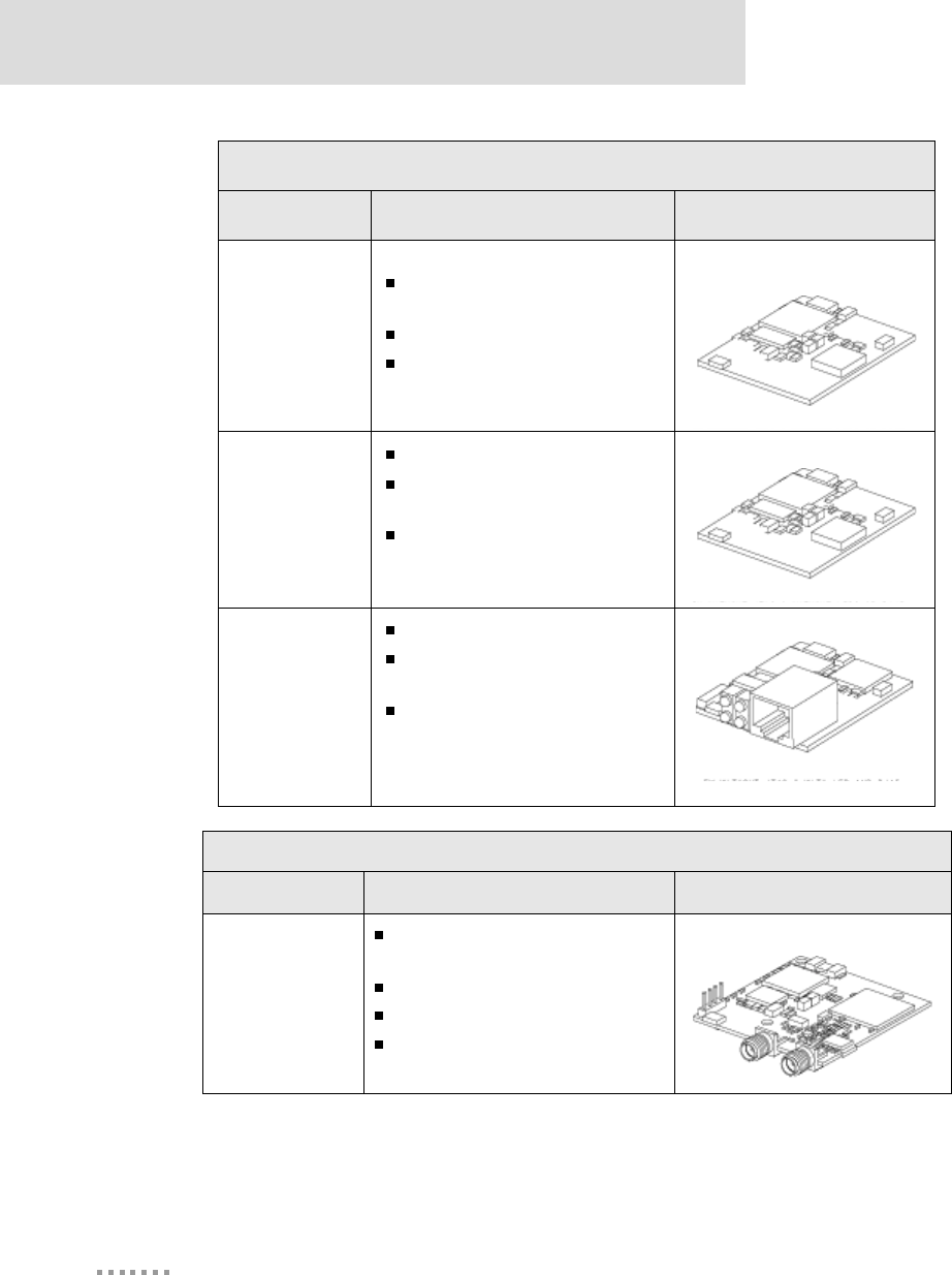
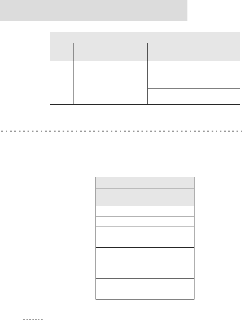
Types of Modules
12
Digi Connect EM & Digi Connect Wi-EM Hardware Reference
DC-EM-02T-ST.C
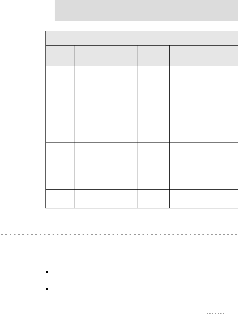
Digi Connect EM Modules
Model Description Figure
DC-EM-02T-JT
Used for development purposes
only
JTAG interface
Pin headers for Ethernet and
LED functionality.
DC-EM-02T-NC
No JTAG interface
Pin headers for Ethernet and
LED functionality
Ordered independently of
development kit for use in your
implementation
DC-EM-02T-S
DC-EM-02T-C
No JTAG interface
RJ-45 Ethernet connector and
LED array
Ordered independently of either
the development or integration
kit for use in your
implementation.
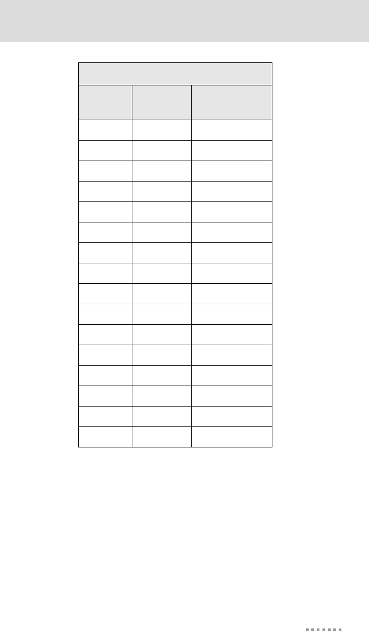
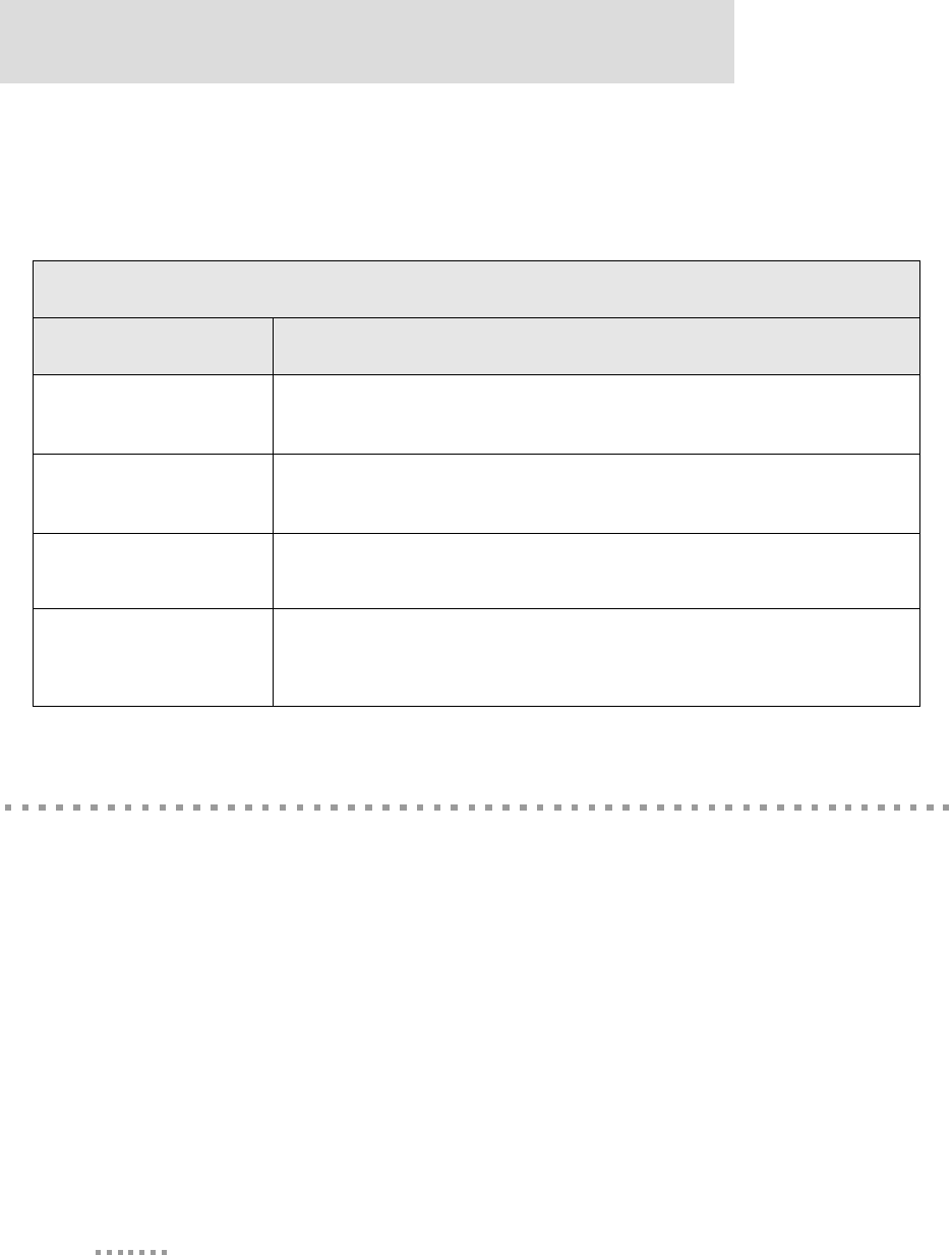
Digi Connect Wi-EM Modules
Model Description Figure
DC-WEM-02T-JT
Used for development purposes
only
JTAG interface
Pin headers LED functionality
Dual RP-SMA Antenna
Connector.
13
About the Embedded Module
Note
-S: No JTAG, w/ LED array, w/RJ-45/antenna connectors, for use with Digi
Firmware
-C: No JTAG, w/LED array, RJ-45 / antenna connectors, for use with Custom
Firmware
-NC: No JTAG, w/LED pin header, w/o RJ-45 connector (for Digi Connect
EM), w/antenna connectors (for Digi Connect Wi-EM), for use with custom
firmware (not shown)
-JT: w/ JTAG, w/pin header, w/o RJ-45 connector (for Digi Connect EM), w/
antenna connectors (for Digi Connect Wi-EM), for use with custom firmware
development
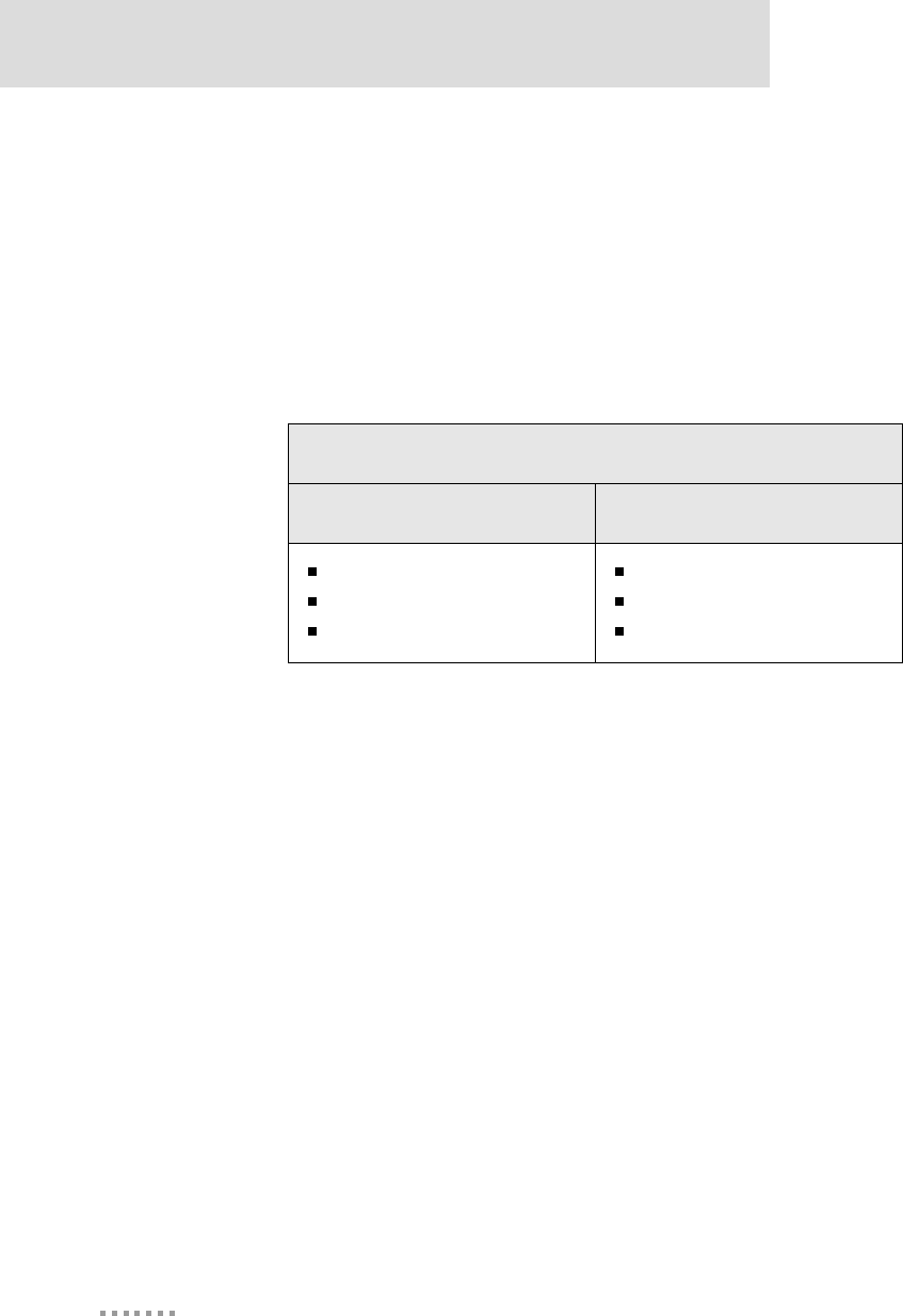
Digi Connect Wi-EM Antennae
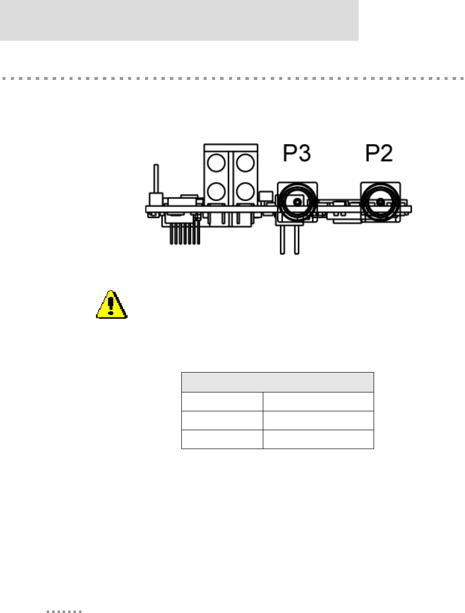
The Digi Connect Wi-EM is available with dual-diversity antenna connectors. The right
antenna (P2) is always used for transmit and receive.The left antenna is receive only. The
antenna will choose the best signal (pin vs. socket). The Digi Connect Wi-EM always has
two antenna connectors but using the second antenna is optional.
The antennae are connected to the module with reverse polarity SMA connectors (sub-
miniature size A). The antennae fit the connectors on the module only one way to ensure a
proper connection. The antennae function best when placed perpendicular to each other
(one straight, the other up or down) to prevent interference from each other.
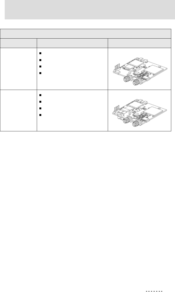
DC-WEM-02T-NC
No JTAG interface
Pin headers LED functionality
Dual RP-SMA Antenna Connector
Ordered independently of
development kit for use in your
implementation
DC-WEM-02T-C
DC-WEM-02T-S
No JTAG interface
LED array
Dual RP-SMA Antenna Connector
Ordered independently of either
development or integration kit for
use in your implementation.
Digi Connect Wi-EM Modules
Model Description Figure
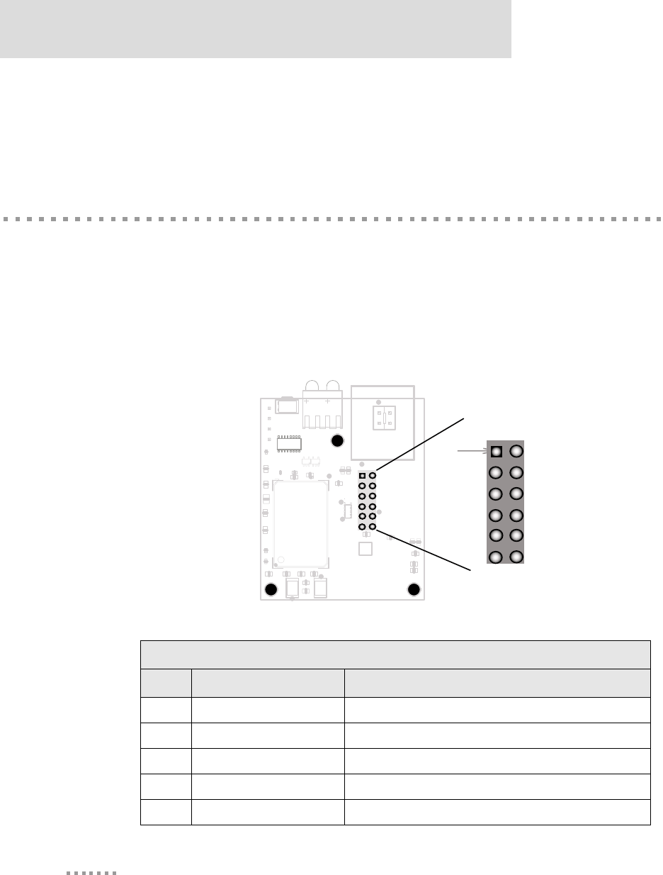
Connectors: Power and Serial Interface
14
Digi Connect EM & Digi Connect Wi-EM Hardware Reference
Another option for both signal reception and design flexibility is to use a "pig tail" cable
Digi part number DC-ANT-EC to separate the antenna from the module. This allows the
module to fit inside your product but the antenna to be placed outside the device.
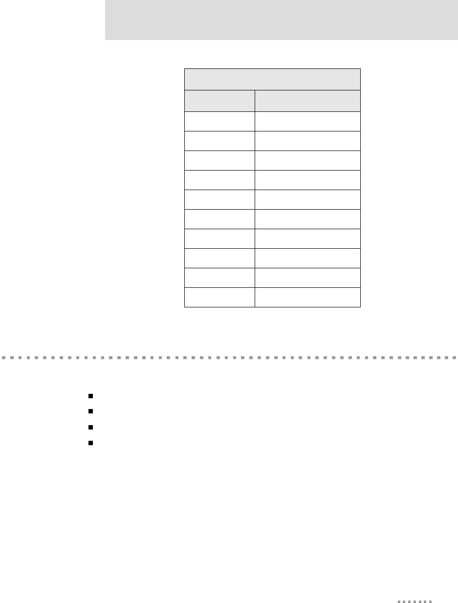
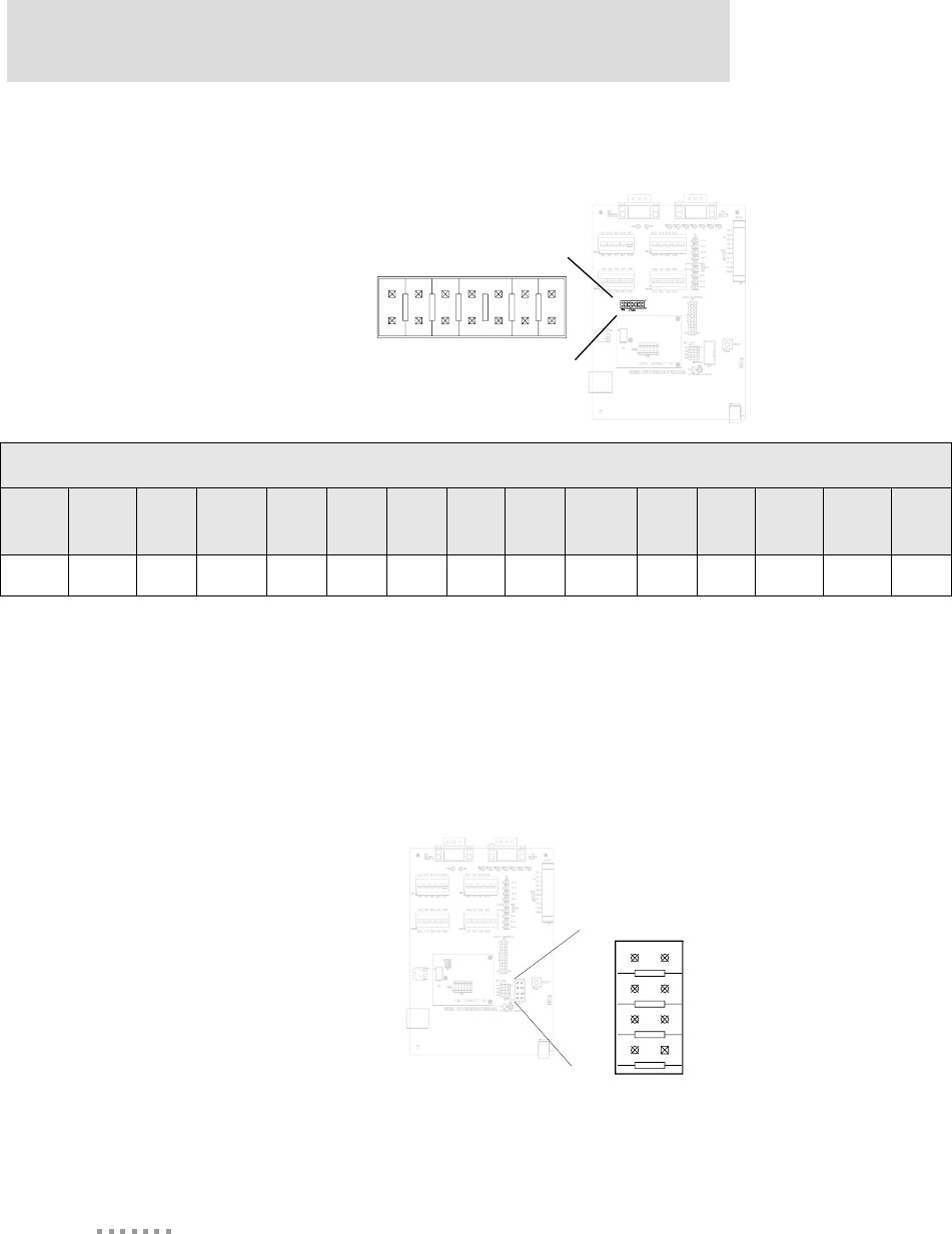
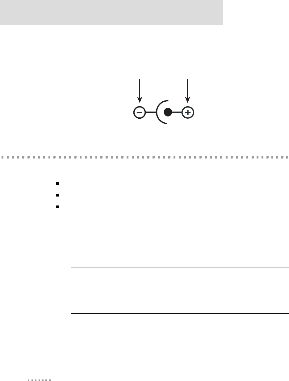
Connectors: Power and Serial Interface
This single 12-pin, serial interface port (labeled P4 for Digi Connect EM and P5 for Digi
Connect Wi-EM) supports 2 TTL serial interfaces, data rates up to 230 Kbps and full-
modem control (on port 1). See the figure for help locating pins and the table for pin
assignments.
Power and Serial Interface
Power and Serial Interface Pin Assignments
Pin Signal Name Description and Notes
1 VCC +3.3 VDC (input only)
2 GND Reference Ground for input power
3 RXD/GPIO-7 Port 1 RXD (input)/GPIO-7
4 TXD/GPIO-6 Port 1 TXD (output)/GPIO-6
5 RTS/GPIO-4/SPI_CLK Port 1 RTS/GPIO-4/SPI clock
GRN
GRN
RED
YEL
PIN1
PIN1
pin 1 2
34
56
78
910
11 12
15
About the Embedded Module
Connectors: Ethernet Interface
The following table shows the pinout of the RJ-45 connector..
For a diagram of the Digi Connect Ethernet pin header location and assignments see "Digi
Connect EM Pin Header Locations" on page 19.
6 DTR/GPIO-5 Port 1 DTR (output)/GPIO-5
7 CTS/GPIO-2 Port 1 CTS (input)/GPIO-2
8 DCD/GPIO-1/SPI_EN Port 1 DCD (input)/GPIO-1/SPI enable
9 DSR/GPIO-3 Port 1 DSR (input)/GPIO-3
10 /RST Reset (input)
11 RXD/GPIO-9 Port 2 RXD (input)/GPIO-9
12 TXD/GPIO-8 Port 2 TXD (output)/GPIO-8
Power and Serial Interface Pin Assignments
Pin Signal Name Description and Notes
RJ-45 Ethernet Interface
Pin # 1 2 3 4 5 6 7 8
Signal TXD+
(Transmit
Data)
TXD-
(Transmit
Data)
RXD+
(Receive
Data)
Not used Not used
RXD-
(Receive
Data)
Not used Not used
Connectors: Antenna
16
Digi Connect EM & Digi Connect Wi-EM Hardware Reference
Connectors: Antenna
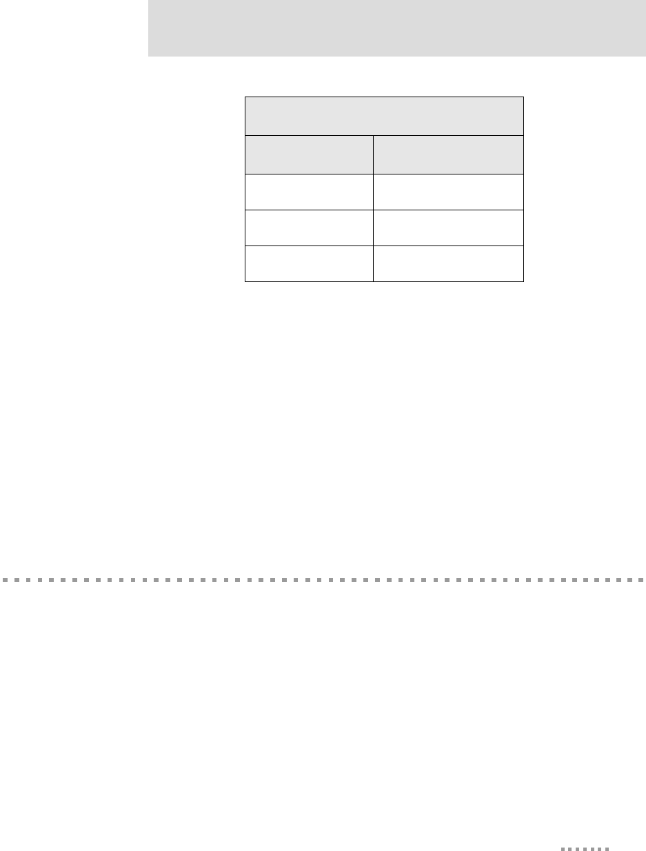
The Digi Connect Wi-EM has 2 RP-SMA antenna connectors labeled P2 and P3.
Wi-EM Antenna Connectors
Antenna Specifications
Type Dipole
Part number DC-ANT-24DP
Gain 2 dBi
Caution: This Part 15 radio device operates on a non-interference basis
with other devices operating at this frequency when using the antennae
listed in the Antenna Specification table. Any changes or modification to
user’s authority to operate the device.
the product not expressly approved by Digi International could void the
17
About the Embedded Module
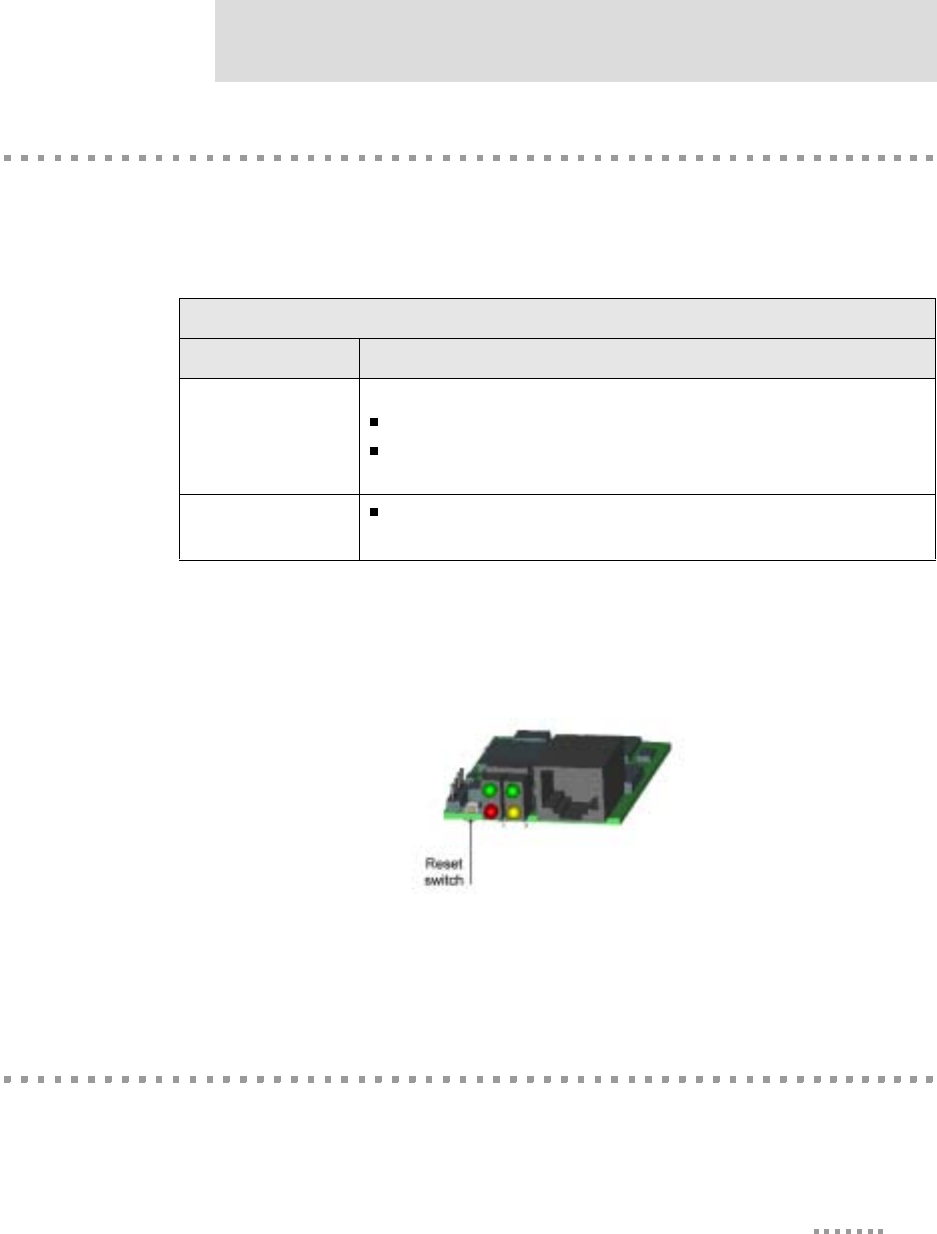
Reset Switch
The behavior of the reset switch is determined by software, which means that it has a
predefined behavior in the integration kit. In the development kit, its behavior is
determined by your implementation. See the following table for details.
Reset Switch Location
Note
The reset switch is in same location for both wired and wireless modules.
Module LEDs
The modules provide two hardware options for LEDs, with or without on board LED array.
The integration kit provides predefined LED behavior. With the development kit, some
Reset Switch Behavior
Kit Behavior
Integration The reset switch does one of the following:
If pressed and released immediately, the device is rebooted.
If pressed and held down (for about 20 seconds) during power-up, the
device is rebooted and restored to the default configuration.
Development The behavior of the switch is user-defined.
See "Embedded Module Reset" on page 42 for more information.
Module LEDs
18
Digi Connect EM & Digi Connect Wi-EM Hardware Reference
LED behavior can be determined by your implementation. See the following table for more
information..
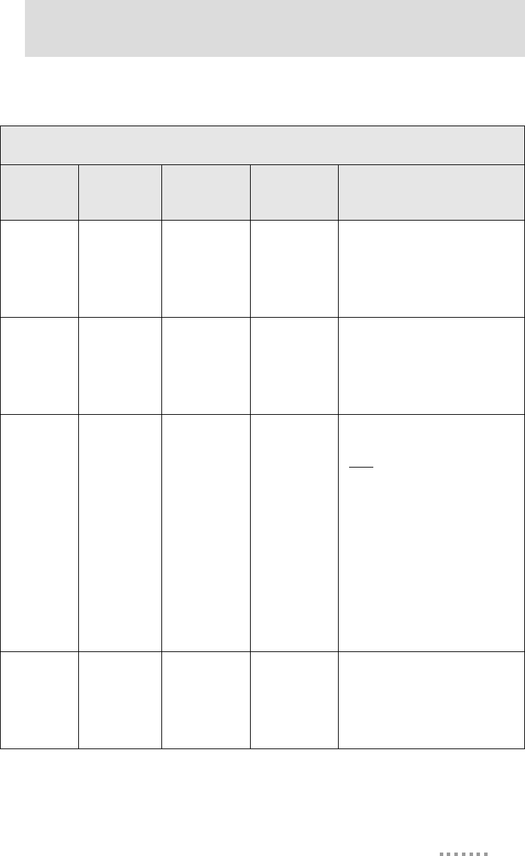
LED Behaviors
LED Pin
Header
EM
Integration Kit
Digi Connect EM Integration Kit
Digi Connect Wi-EM Development
Kit
Top left
(green)
1 (+)
3 (-)
Serial port activity:
Off - the serial channel is idle.
Blinking - serial data is transmitted or received.
This LED is
software
programmable
Top
right
(green)
5 (+)
7 (-)
Network link status:
Off - no link has been detected.
On - a link has been detected.
Network link status:
On - unit is associated with an access point
Blinking slowly - unit is in ad hoc mode
Blinking quickly - unit is scanning for a
network
Same as
Integration Kit
(Network link
status)
Bottom
left (red)
2 (+)
4 (-)
Diagnostics:
Blinking 1-1-1 - starting the operating system.
Blinking 1-5-1 - configuration has been returned to factory defaults.
Note: If other blinking patterns occur, contact Digi Technical Support.
This LED is
software
programmable
Bottom
right
(yellow)
6 (+)
8 (-) Blinking - network data is transmitted or received
This LED is
software
programmable
19
About the Embedded Module
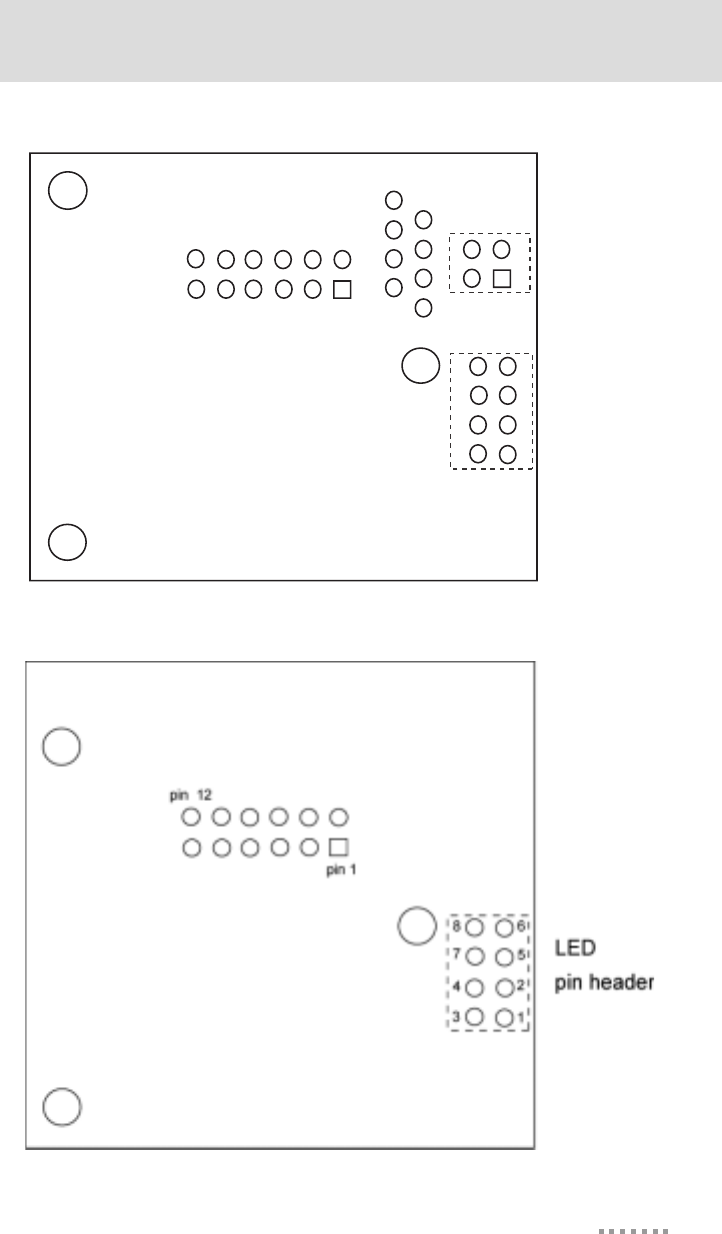
Digi Connect EM Pin Header Locations
Digi Connect Wi-EM Pin Header Locations
4
1
1
2
5
6
3
4
7
8
2
3
pin 12
pin 1
Ethernet
pin heade
r
LED
pin header

Module LEDs
20
Digi Connect EM & Digi Connect Wi-EM Hardware Reference

21
About the Development
Board
CHAPTER 2
Overview
This chapter provides information on the development board, a hardware platform from
which you can determine how to integrate the embedded module into your design. For
additional information, see the schematic and mechanical drawings. If you have installed
the development kit or integration kit, you can access the schematic from the Start menu.
Basic Description
The development board can be used by both module feature sets with the Integration Kit or
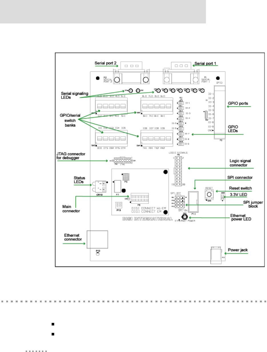
the Development Kit.The following graphic is a layout of the development board.
23
About the Development Board
GPIO Port (P3)
Serial Port 1 (P1) and Serial Port 2 (P2)
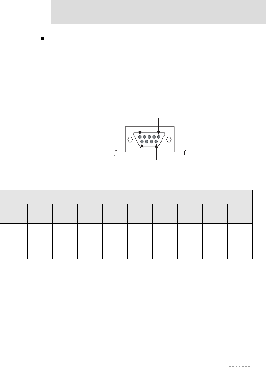
Serial port 1 and port 2 are DB-9 male connectors labeled P1 and P2. Use the following
figure and table for pin orientation and pin assignment information.
Serial Port Pin Orientation
0
0000006
Pin 1 Pin 5
Pin 6 Pin 9
Serial Pin Assignment
Port Signal
Pin 1 Signal
Pin 2 Signal
Pin 3 Signal
Pin 4 Signal
Pin 5 Signal
Pin 6 Signal
Pin 7 Signal
Pin 8 Signal
Pin 9
1DCD RXD TXD DTR GND DSR RTS CTS Not
Connected
2Not
Connected RXD TXD Not
Connected GND Not
Connected
Not
Connected
Not
Connected
Not
Connected
Ports
24
Digi Connect EM & Wi-EM Hardware Reference
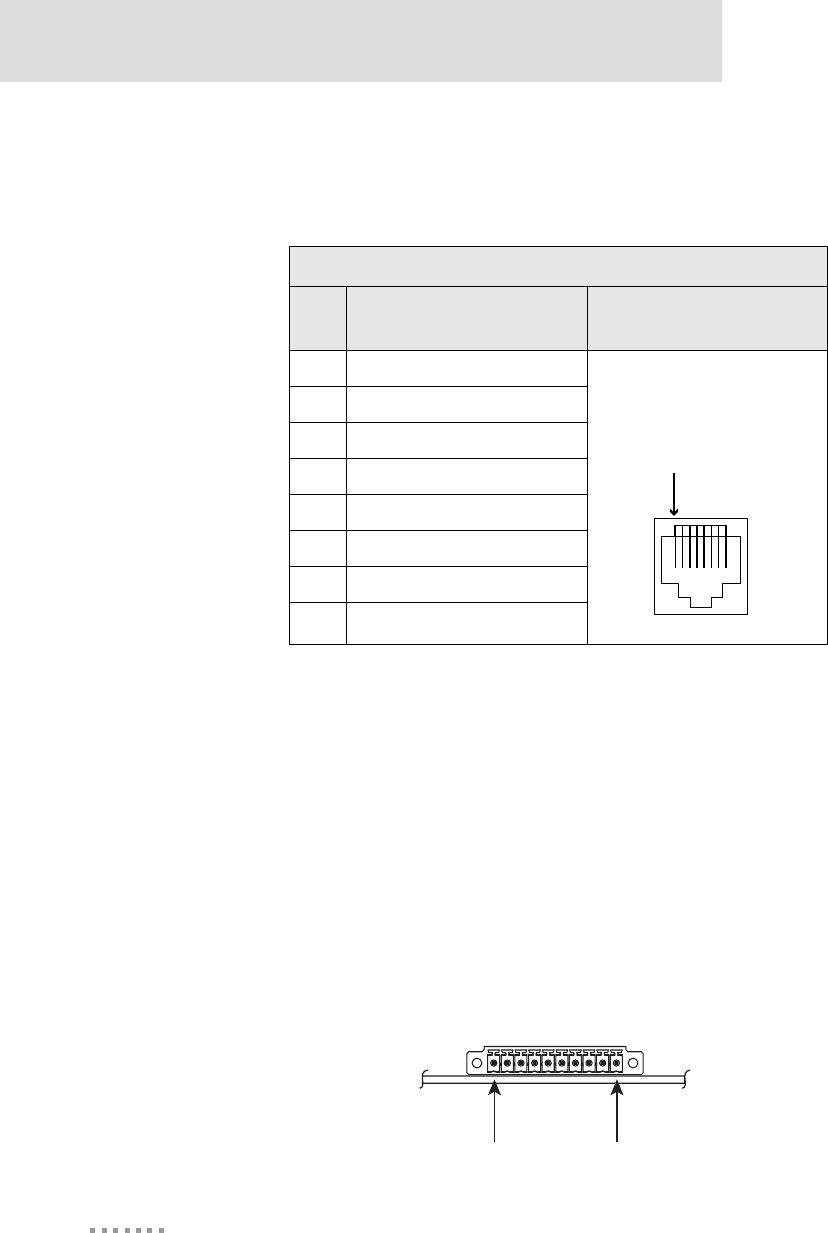
Ethernet Port (P12)
The Ethernet port of the Digi Connect EM embedded module (labeled P12) is an 8-pin
RJ-45 jack meeting the requirements of ISO 8877 for 10/100Base-T. When two
descriptions are shown for a pin, the second is for use with 802.3af powered Ethernet.
For additional information about the 802.3af standard, refer to the corresponding IEEE
specification.
Note
The development board provides a reference design of a POE (Power Over
Ethernet) power supply. A schematic for this reference design is installed by
the setup program on the CD.
GPIO Port (P3)
The GPIO port is a 10-pin male right-angle connector (labeled P3). See the following
figure and table for pin orientation and pin assignments.
GPIO Port Pin Orientation
Ethernet Pin Assignments
Pin Signal Name Figure
RJ-45 (P12)
1 TXD+ (Transmit Data)
2 TXD- (Transmit Data)
3 RXD+ (Receive Data)
4 Not used / power (+)
5 Not used / power (+)
6 RXD- (Receive Data)
7 Not used / power (-)
8 Not used / power (-)
Pin
1
Pin 1 Pin 10
0
0000020
25
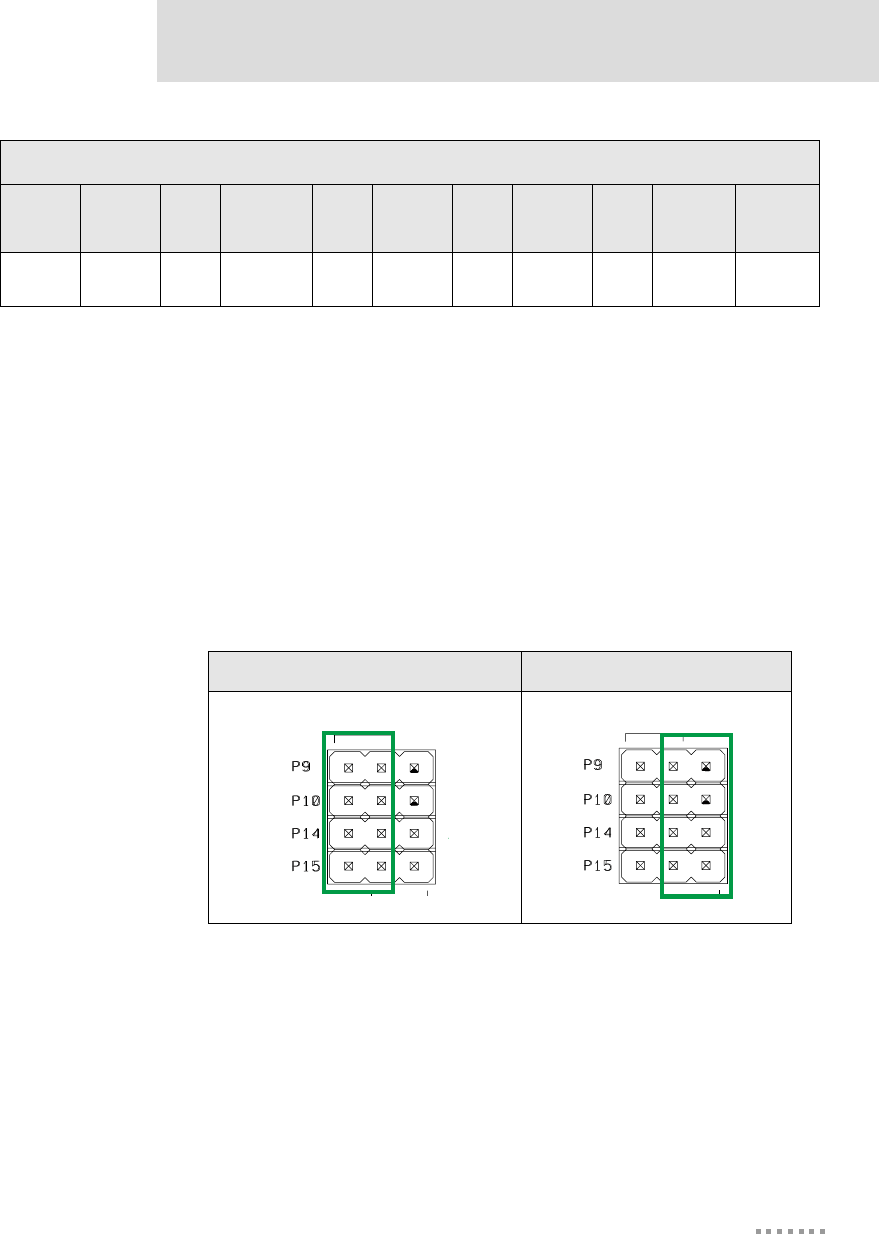
About the Development Board
Connectors and Blocks
The development board provides the following connectors and blocks:
JTAG Debugger Connector (P4)
SPI Connector (P11) and SPI Jumper Block
Logic Signal Analyzer Header (P6)
Main Connector (P8)
JTAG Debugger Connector (P4)
This 14-pin male vertical header labeled P4 mates with a JTAG debugger plug (for
example, a Macraigor Raven). It is used with the development kit only. See the following
figure and table for pin orientation and assignments.
GPIO Port Pin Assignments
Pin Signal Name
1GND
2GPIO-9
3GPIO-8
4GPIO-7
5GPIO-6
6GPIO-5
7GPIO-4
8GPIO-3
9GPIO-2
10 GPIO-1
Connectors and Blocks
26
Digi Connect EM & Wi-EM Hardware Reference
JTAG Debugger Connector Pin Orientation
SPI Connector (P11)
This connector is used for a Serial Peripheral Interface (SPI) connection. When enabled,
signals are disconnected from serial port 1 and GPIO connectors. See the following figure
and table for pin orientation and pin assignments.
SPI Connector Pin Orientation
pin
1
2
13
14
JTAG Debugger Connector Pin Assignments
Pin
1Pin
2Pin
3Pin
4Pin
5Pin
6Pin
7Pin
8Pin
9Pin
10 Pin
11 Pin
12 Pin
13 Pin
14
Signal VCC+ GND /TRST GND TDI GND TMS GND TCK GND TDO /SRST VCC+ GND
Pin 1Pin 2
Pin 7
Pin 8
27
About the Development Board
SPI Jumper Block
The SPI jumper block determines whether the SPI connector is connected or not. If SPI is
off (the default), serial and GPIO signals are routed to switch banks 1 through 4. (See
"Serial/GPIO Switch Bank 3 (SW3) and Switch Bank 4 (SW4)" on page 31 and "GPIO
Switch Bank 1 (SW1) and 2 (SW2)" on page 32.) If SPI is on, SPI signals are routed to the
SPI connector (P11).
The following figures demonstrate how to set the SPI jumper block
SPI Jumper Settings
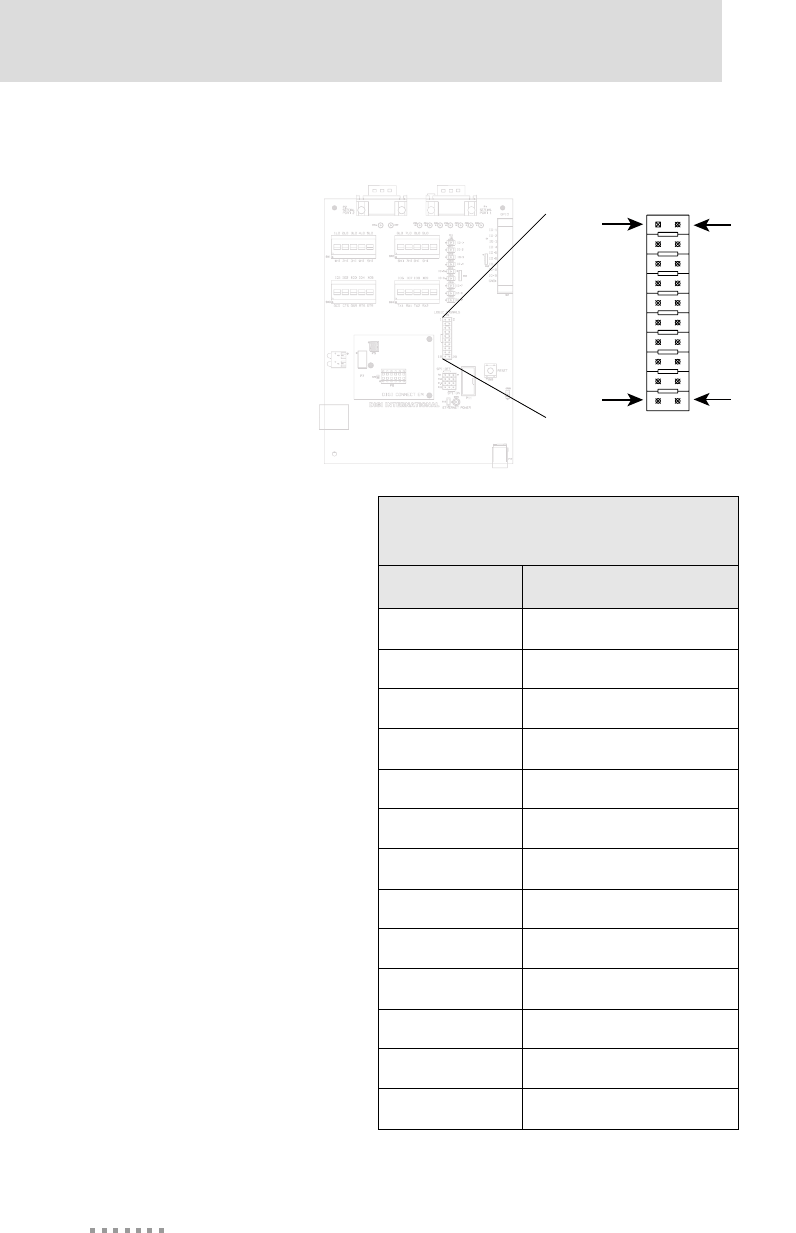
Logic Signal Analyzer Header (P6)
This 20-pin male vertical header (labeled P6) connects a digital signal analyzer (for
example, a logic analyzer) to the development board. It is used with the development kit
only. See the following figure and table for pin orientation and pin assignments.
SPI Pin Assignments
Pin
1Pin
2Pin
3Pin
4Pin
5Pin
6Pin
7Pin
8Pin
9Pin
10
Signal SPI-EN GND SPI-CLK GND SPI-TX GND SPI-RX GND Not
connected
Not
connected
SPI OFF SPI ON
oo
Connectors and Blocks
28
Digi Connect EM & Wi-EM Hardware Reference
Logic Analyzer Header Pin Orientation
Logic Analyzer Header Pin
Assignments
Pin Signal
1 - 8 Not connected
9/RST
10 Not connected
11 DTR/GPIO-5
12 TXD-2/GPIO-8
13 CTS/GPIO-2
14 RXD-2/GPIO-9
15 DSR/GPIO-3
16 TXD-1/GPIO-6
17 RTS/GPIO-4/SPI_CLK
18 RXD-1/GPIO-7
19 DCD/GPIO-1/SPI_EN
20 GND
Pin 2
Pin 20
Pin 1
Pin 19
29
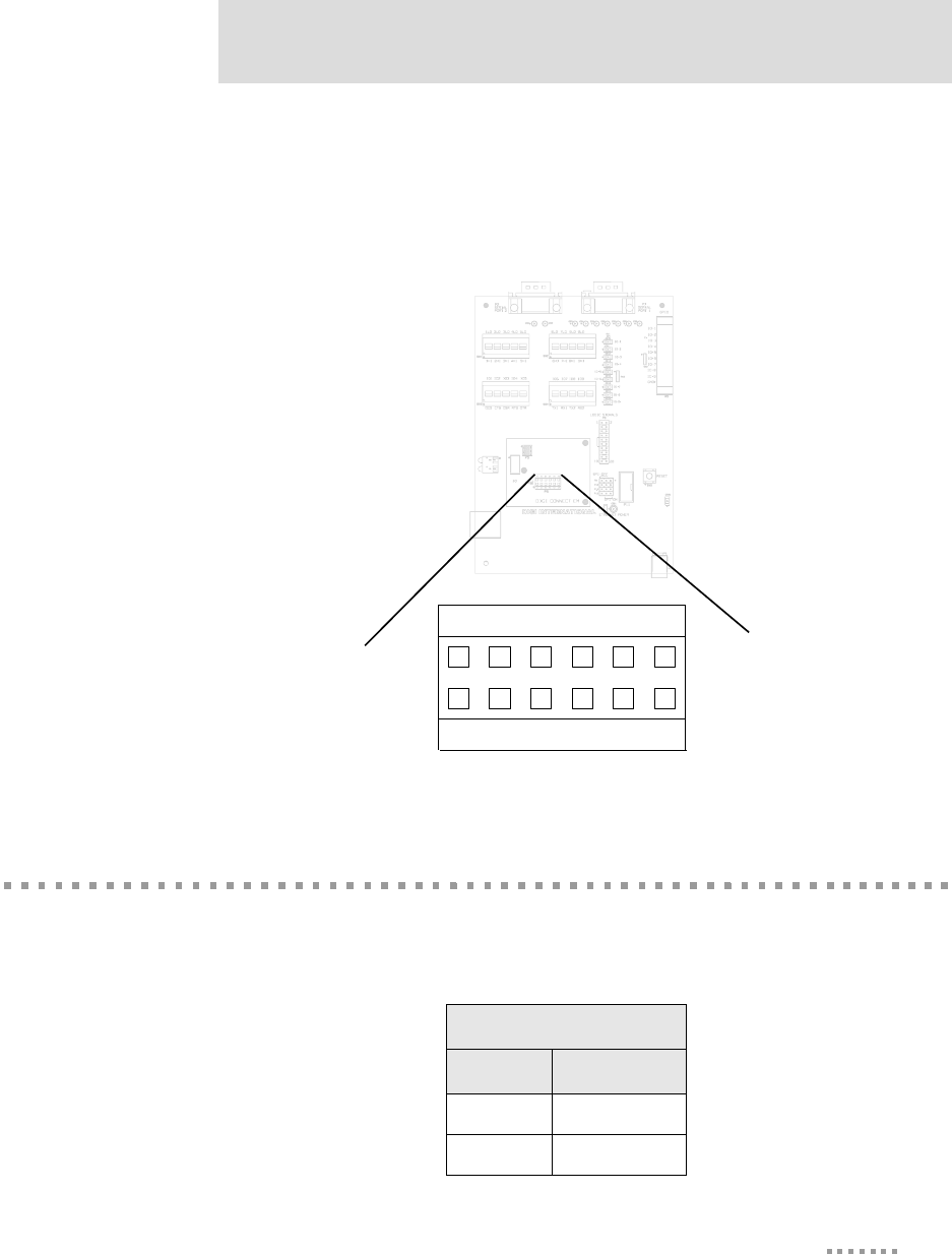
About the Development Board
Main Connector (P8)
This 12-pin connector is used to interface with the embedded module. See the following
figure for pin orientation.
Main Connector Pin Orientation
Power Jack (P17)
The Power Jack is a barrel connector that accepts 9 to 30 VDC +/- 5%. The jack is labeled
P17. The following table shows the polarity of the power jack.
Pin 1 Pin 11
Pin 2 Pin 12
Power Jack Polarity
Contact Polarity
Center +9 to +30 VDC
Outer Ground
Switches
30
Digi Connect EM & Wi-EM Hardware Reference
The following figure schematically represents the polarity of the power jack
Power Jack Polarity Schematic.
Switches
The development board provides the following switches:
Reset Switch (SW5)
Serial/GPIO Switch Bank 3 (SW3) and Switch Bank 4 (SW4)
GPIO Switch Bank 1 (SW1) and 2 (SW2)
Reset Switch (SW5)
This push button switch is labeled SW5. Pressing it sets the module’s /RST line low,
holding the module in a hard reset until the switch is released.
Note: This is a "hard" reset using the /RST pin on the main connector, not a "soft" reset.
The reset button on the embedded module performs a "soft" reset (see also "Main
Connector (P8)" on page 29).
Ground +9 to +30 VDC
31
About the Development Board
Serial/GPIO Switch Bank 3 (SW3) and Switch Bank 4 (SW4)
Each switch bank holds five slide switches that enable either serial or GPIO signaling
between the development board and the module. When set for GPIO signaling, SW3 works
in conjunction with SW1, and SW4 works with SW2. See "GPIO Switch Bank 1 (SW1)
and 2 (SW2)" on page 32 for more information. See the following table for SW3 and SW4
switch definitions.
Note: These switches control where the development board routes a signal. They do not
reconfigure the NS7520 processor. Software should be configured to track with switch
settings. See "GPIO" on page 37 for more information.
GPIO Switch Banks 3 and 4 Settings
Switch
Bank Switch
Number Left
Position Right
Position
SW3
1DCDGPIO-1
2CTSGPIO-2
3DSRGPIO-3
4RTSGPIO-4
5DTRGPIO-5
SW4
6 TXD-1 GPIO-6
7 RXD-1 GPIO-7
8 TXD-2 GPIO-8
9 RXD-2 GPIO-9
10 Not connected Not connected
Development Board LEDs
32
Digi Connect EM & Wi-EM Hardware Reference
GPIO Switch Bank 1 (SW1) and 2 (SW2)
GPIO Switch Bank 1 and Switch Bank 2, labeled SW1 and SW2, are two sets of five slide
switches that set GPIO inputs to logic levels of high (switch to left) or low (switch to
right).
If the GPIO port is configured as an output, then the switch should always be to the left. If
there is an external device connected to P3, the switch should always be set to the left.
Each GPIO port can be used independently.
Notes:
These switches do not determine whether the GPIO is an input or output. That
is determined by the module software.
If GPIO is set to an output by software, switches must be set to the left (high).
These switches are used in conjunction with SW3 and SW4.
Development Board LEDs
The development board contains 21 LEDs labeled CR1 through CR21. The following table
lists and describes the LEDs.
LED Descriptions
Board
Label Description
Color or State
Indication
CR1 TXD-2 Flickering Serial activity
Green Inactive
CR2 RXD-2 Flickering Serial activity
Green Inactive
CR3 CTS
Yellow Active
Green Inactive
Off Not connected or signal
not being driven
33
About the Development Board
CR4 DTR
Yellow Active
Green Inactive
Off Not connected or signal
not being driven
CR5 TXD-1 Flickering Serial activity
Green Inactive
CR6 RXD-1 Flickering Serial activity
Green Inactive
CR7 RTS
Yellow Active
Green Inactive
Off Not connected or signal
not being driven
CR8 DCD
Yellow Active
Green Inactive
Off Not connected or signal
not being driven
CR9 DSR
Yellow Active
Green Inactive
Off Not connected or signal
not being driven
CR10 -18
GPIO-1 through GPIO-9.
(CR10=GPIO-1, CR11=GPIO-2, etc.
All can be used for input or output.)
On Logic high
Off Logic low
CR20 3.3V Indicator On Power on
Off Power off
LED Descriptions
Board
Label Description
Color or State
Indication
Test Points
34
Digi Connect EM & Wi-EM Hardware Reference
Test Points
The development board provides 25 test points that can be identified by board label or test
point number. The board labels are adjacent to each test point on the board. The test point
numbers are in the development board schematic drawings. The following table lists the
test point number, board label, and a brief description of each test point.
CR21 EPWR, Powered Ethernet Enabled
On
Ethernet power present
from external powered
Ethernet connector
(Ethernet hub or switch)
Off No powered Ethernet
voltage
LED Descriptions
Board
Label Description
Color or State
Indication
Test Point Descriptions
Test
Point Board
Label Description
TP2 TXD TXD-2
TP3 RXD RXD-2
TP4 CTS CTS
TP5 DTR DTR
TP6 TXD TXD-1
TP7 RXD RXD-1
TP8 RTS RTS
TP9 DCD DCD
TP10 DSR DSR
35
About the Development Board
TP11 IO-1 GPIO-1
TP12 IO-2 GPIO-2
TP13 IO-3 GPIO-3
TP14 IO-4 GPIO-4
TP15 IO-5 GPIO-5
TP17 3.3V 3.3V Supply
TP20 RESET Reset (active low)
TP21 E+ Ethernet Power +
TP22 E- Ethernet Power -
TP23 V-IN 9-30 VDC Input
TP24 GND Ground
TP25 GND Ground
TP26 IO-8 GPIO-8
TP27 IO-7 GPIO-7
TP28 IO-6 GPIO-6
TP29 IO-9 GPIO-9
Test Point Descriptions
Test
Point Board
Label Description

Test Points
36
Digi Connect EM & Wi-EM Hardware Reference

37
Programming
Considerations
CHAPTER 3
This chapter addresses the embedded modules programming considerations.
Note
This chapter applies only to development kit customers.
GPIO
General Information
The NS7520 processor supports 16 general purpose I/O (GPIO) lines, some of which are
reserved for specific functions and some of which can be customized. These GPIO lines
fall into three categories:
Those labeled “Reserved” in the following table are reserved for a specific use
and must not be reprogrammed, or the unit may not operate correctly. Often,
these lines are not connected to external interfaces.
Those labeled “Allocated” in the following table are exposed to an external
interface and allocated to a specific use by the software, but they can be
customized safely with code modifications.
Those labeled “Available” are exposed to an external interface, not controlled
directly by the software, and can be customized.
GPIO
38
Digi Connect EM & Wi-EM Hardware Reference
GPIO Registers
Two registers, PORTA and PORTC, govern the 16 GPIO pins. Each is responsible for eight
GPIO pins, and each pin has four bits that completely describe its behavior. The four bits
that describe the GPIO behavior are its mode (CMODE), direction (CDIR), special
function (CSF--only applicable to PORTC), and data value. The first three bits describe the
functionality of the GPIO pin. The "data" bit provides the current value of the pin when
read and allows control of the value of an output pin when written. Use the following table
for information on configuring a bit position in the appropriate register for GPIO input or
output.
Since each register controls 8 GPIO lines, it is safest to read the full 32 bit register, modify
the bits corresponding to the GPIO line of interest, and then write the full 32 bits back. In
this way, the behavior of the other GPIO lines will be preserved.
For more information regarding the format and programming of the GPIO registers, see the
NS7520 Hardware Reference.
Configuring a GPIO Pin for Input and Output
Input Output
CMODE = 0
CDIR = 0
CSF = 0
CMODE = 0
CDIR = 1
CSF = 0
39
Programming Considerations
GPIO Pin Use
GPIO Pin Use
Name Register
Bit Category External
Interface Description
TXD/
GPIO-6 PORTA7 Allocated Pin 4 on the
main header
Used for port 1 serial transmit but
can be reassigned as GPIO input
or output. If used with the
development board, this pin maps
to GPIO-6.
DTR/
GPIO-5 PORTA6 Allocated Pin 6 on the
main header
Used for the port 1 serial DTR
signal but can be reassigned as
GPIO input or output. If used
with the development board, this
pin maps to GPIO-5.
See the
description
PORTA5,
PORTA4 Allocated Pin 5 on the
main header
Since these two processor pins
map to the same header pin, one
must be configured as an input to
avoid contention. Under normal
serial conditions, PORTA5 is
configured to deliver the port 1
RTS signal and PORTA4 for
GPIO input. To use the port for
SPI, configure PORTA5 for
GPIO input and PORTA4 to
deliver SPI clock.
When used with the development
board, header pin 5 maps to
GPIO-4.
RXD/
GPIO-7 PORTA3 Allocated Pin 3 on the
main header
Used for port 1 serial receive but
can be reassigned as GPIO input
or output. If used with the
development board, this pin maps
to GPIO-7.

GPIO
40
Digi Connect EM & Wi-EM Hardware Reference
DSR/
GPIO-3 PORTA2 Allocated Pin 9 on the
main header
Used for the port1 serial DSR
signal but can be reassigned as
GPIO input or output. If used
with the development board, this
pin maps to GPIO-3.
CTS/
GPIO-2 PORTA1 Allocated Pin 7 on the
main header
Used for the port 1 serial CTS
signal but can be reassigned as
GPIO input or output. If used
with the development board, this
pin maps to GPIO-2.
DCD/
GPIO-1 PORTA0 Allocated Pin 8 on the
main header
Used for the port 1 serial DCD
signal but can be reassigned as
GPIO input or output. If used
with the development board, this
pin maps to GPIO-1.
TXD2/
GPIO-8 PORTC7 Allocated Pin 12 on the
main header
Used for port 2 serial transmit but
can be reassigned as GPIO input
or output. If used with the
development board, this pin maps
to GPIO-8.
Power
indicator
LED
PORTC6 Allocated Connected to
the red LED
Used as the power indicator
(always on) but can be reassigned
as a general purpose LED. It must
remain a GPIO output for the
LED to operate correctly. This
LED is lit when the signal is low.
/INIT PORTC5 Available
Connected to
the button on
the module
Should be configured as a GPIO
input.
GPIO Pin Use
Name Register
Bit Category External
Interface Description
41
Programming Considerations
Embedded Module LEDs
General information
The embedded module has two types of LEDs:
LEDs connected directly to GPIO pins on the processor and controlled directly
in software
LEDs connected to other hardware components (Ethernet/wireless hardware)
and not directly programmable by the operating system
Green
LED PORTC4 Allocated
Connected to
the green
LED (the one
above the red
LED)
Used as the NET+OS green LED
but can be reassigned as a general
purpose LED. It must remain a
GPIO output for the LED to
operate correctly. The LED is lit
when the signal is low.
RXD2/
GPIO-9 PORTC3 Allocated Pin 11 on the
main header
Used for port 2 serial receive but
can be reassigned as GPIO input
or output. If used with the
development board, this pin maps
to GPIO-9.
Yellow
LED PORTC2 Allocated
Connected to
the yellow
LED
Used as the NET+OS yellow
LED but can be reassigned as a
general purpose LED. It must
remain a GPIO output for the
LED to operate correctly. The
LED is lit when the signal is a
low.
PORTC1-
PORTC0 Reserved NA NA
GPIO Pin Use
Name Register
Bit Category External
Interface Description
Embedded Module Reset
42
Digi Connect EM & Wi-EM Hardware Reference
For information on LED control, see the NET+Works BSP Porting Guide.
About Embedded Module LEDs
Embedded Module Reset
Hard Reset
The embedded modules support a hardware reset on pin 10 of the 12-pin header. The unit
will be forced into a hard reset if this pin is pulled low. When used with the development
board, this pin is wired to reset button SW5, which means it acts as a hard reset button.
Embedded Module LED Description
LED Description
Green
(above yellow LED) This LED is wired to the network hardware and provides an indication of link status.
Green
(the one above the red LED)
This LED is software programmable and is wired to processor GPIO register bit
PORTC4 and wired to be lit when low.
Yellow This LED is software programmable, wired to processor GPIO register bit PORTC2,
and wired to be lit when low.
Red
This LED is software programmable, wired to processor GPIO register bit PORTC6,
and wired to be lit when low.The default is that this LED indicates power
(and is therefore always on).
43
Programming Considerations
Soft Reset
NET+OS provides an internal facility to enact a soft reset, but it is the responsibility of a
specific implementation to choose a reasonable trigger to invoke it. One choice is to use a
GPIO pin as a signal to trigger a soft reset. The embedded modules have one GPIO pin
(PORTC5) which is not normally assigned to any other task named "/INIT." It is an ideal
candidate for use as a signal for soft reset. The signal is wired to the push button on the
module (next to the LEDs), and is pulled high unless the button is pushed.
The "naresetapp" sample application demonstrates a simple mechanism for monitoring a
GPIO pin and then initiating a soft reset when the pin achieves a particular value.
Flash
General Information
The embedded modules have 4 MB of flash memory, which is controlled by chip select 0,
located at 0x02000000.
Memory
Both modules have 8 MB of SDRAM memory, controlled by chip select 1, located at
0x00000000 in the processor address space and aliased at 0x04000000 and 0x08000000.
The application program is loaded at address 0x08080000.
Reset Characteristics
Characteristic Specification
Delay 200 milliseconds (typical)
Threshold 2.93 V
Minimum Hold Time 1 microsecond pulse

Flash
44
Digi Connect EM & Wi-EM Hardware Reference

45
Specifications
APPENDIX A
Network Interfaces
Digi Connect Wi-EM Embedded Module
Standard: IEEE 802.11b
Data Rate: Up to 11 Mbps with automatic fallback
Frequency: 2.4 GHz
Modulation: CCK (11/5 Mbps), DQPSK (2 Mbps), DBPSK (1 Mbps)
Transmit power: 16 dBm typical
Receive sensitivity:
– 1Mbps: -92 dBm
– 2Mbps: -89 dBm
– 5.5Mbps: -87 dBm
– 11Mbps: -82 dBm
Antenna connector: 2 x RP-SMA
Digi Connect EM Embedded Module
Standard: IEEE 802.3
Data rate: 10/100 Mbps (auto-sensing)
Mode: Full or half duplex (auto-sensing)
Connector: RJ-45 or pin header
Serial Interface
46
Digi Connect EM & Wi-EM Hardware Reference
Serial Interface
Two serial ports, one with full modem control signals and the other with TXD and RXD
only.
Data Rates (bps)
50, 110, 134, 150, 200, 300, 600, 1200, 2400, 3600, 4800, 9600, 19200, 38400, 57600,
115200, 230400
Flow Control Options
RTS/CTS, XON/XOFF, None
Environmental
DC Characteristics
The following tables provide DC characteristics for operating conditions, inputs, and
outputs.
Digi Connect EM Digi Connect Wi-EM
Ambient Temperature -40oF to 185oF
(-40oC to 85oC)
-4oF to 185oF
(-20oC to 85oC)
Storage Temperature -400F to 2570F
(-400C to 1250C)
Humidty 5% to 90%
Altitude 12000 feet
(3657.60 meters)
47
Specifications
Note
The embedded modules use a supervisory circuit with a 2.93V reset threshold.
When VCC falls to the threshold voltage, a reset pulse is issued, holding the
output in active state. When power rises above 2.93V, the reset remains for
approximately 200 ms to allow the system clock and other circuits to stabilize.
Operating Conditions
Symbol Description Min Typ Max Unit
VCC Supply Voltage 3.14 3.3 3.45 V
ICC Supply Current — —
Digi
Connect
EM
270
mA
Digi
Connect
Wi-EM
400
IIL Input Current as “0”
(57K pull-up) —— 57 µA
IIH Input Current as “1”
(57K pull-up) -10 — 10 µA
IOZ HighZ Leakage Current -10 — 10 µA
IOD Output Drive Strength — — 2 mA
CIO Pin Capacitance (VO=0) — — 4 pF
Inputs
Symbol Description Min Typ Max Unit
VIH Input High Voltage 2 — VCC+0.3 V
VIL Input Low Voltage VSS-0.3 — 0.2*VCC V
Outputs
Symbol Description Min Typ Max Unit
VOH Output High Voltage 2.4 — 3.45 V
VOL Output Low Voltage 0 — 0.4 V
Mechanical
48
Digi Connect EM & Wi-EM Hardware Reference
Mechanical
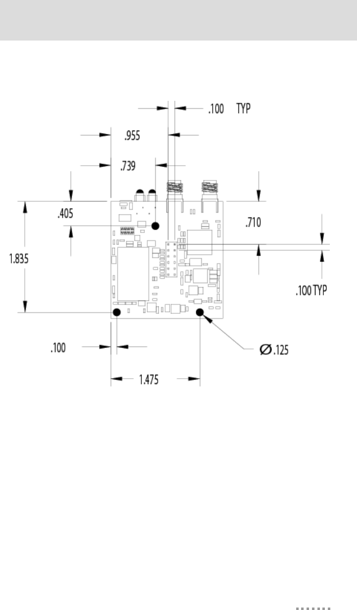
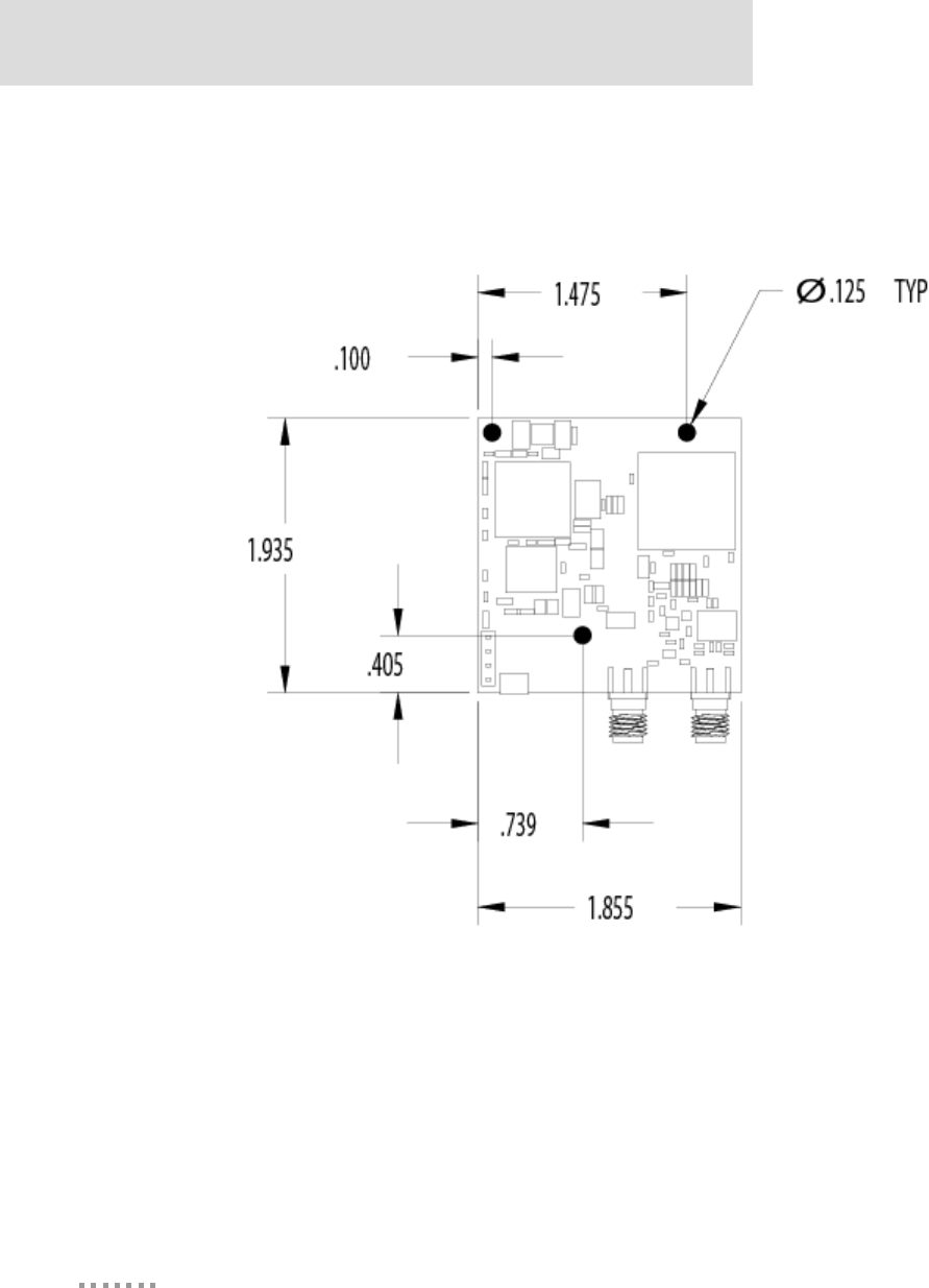
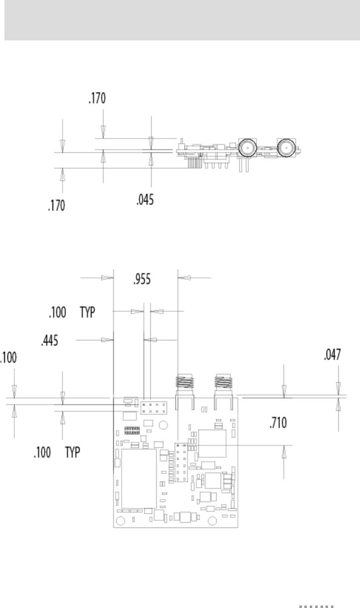
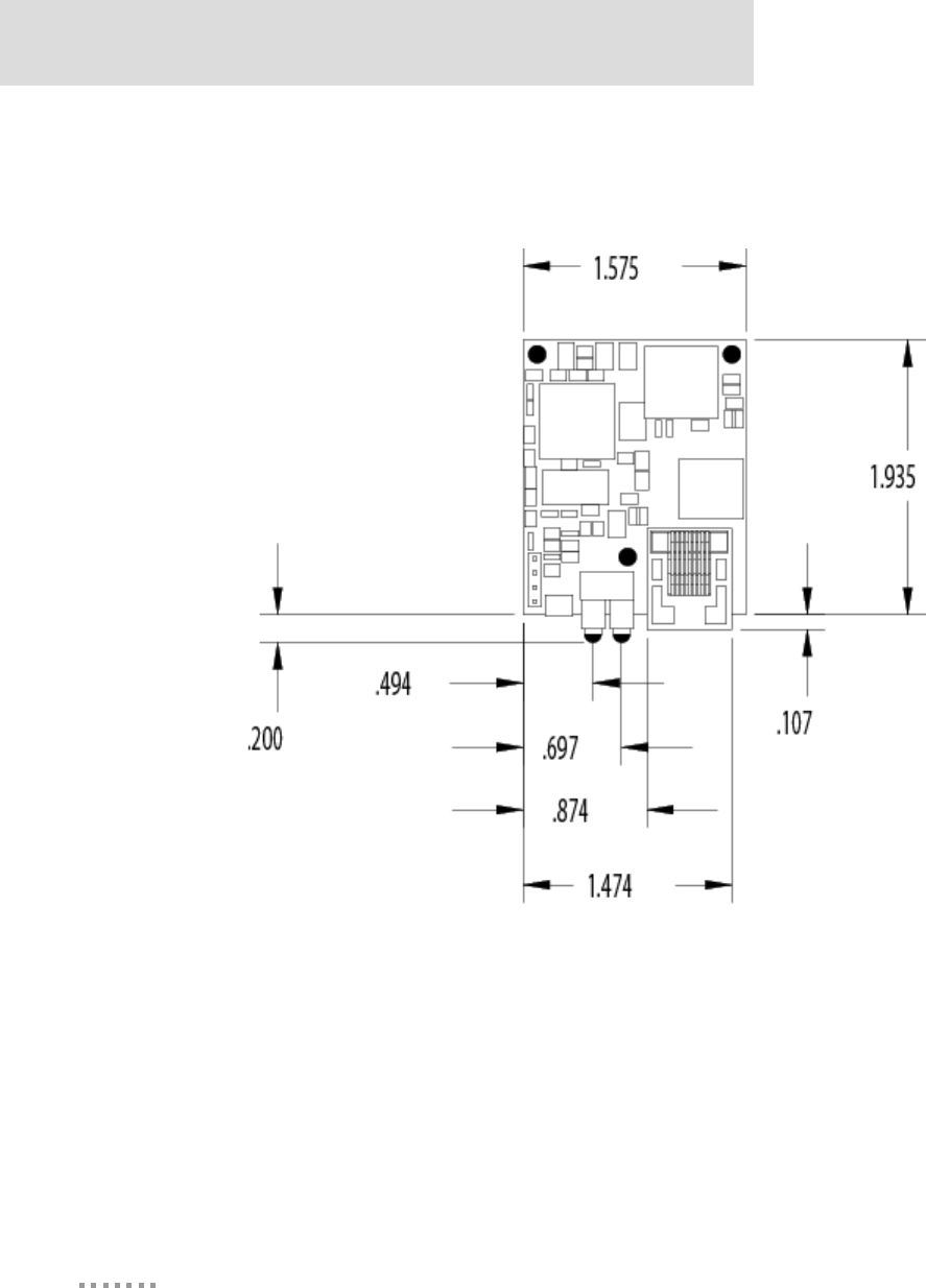
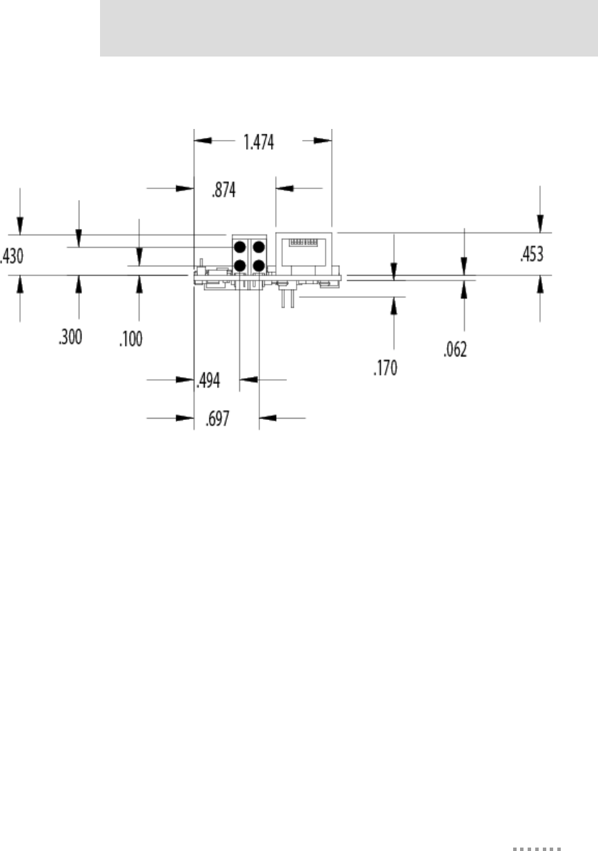
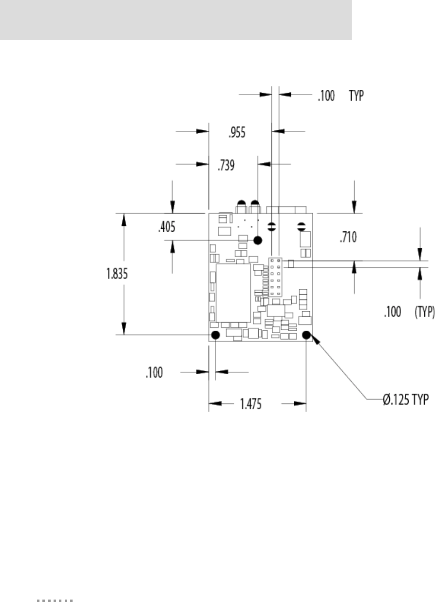
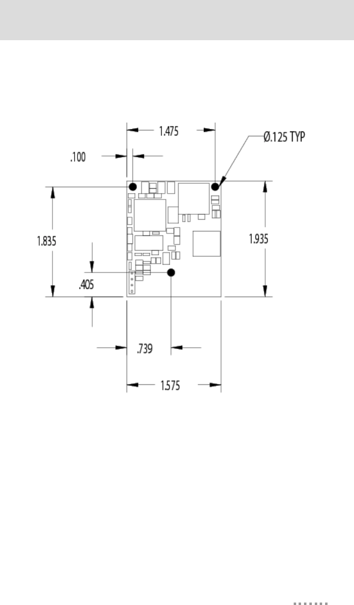
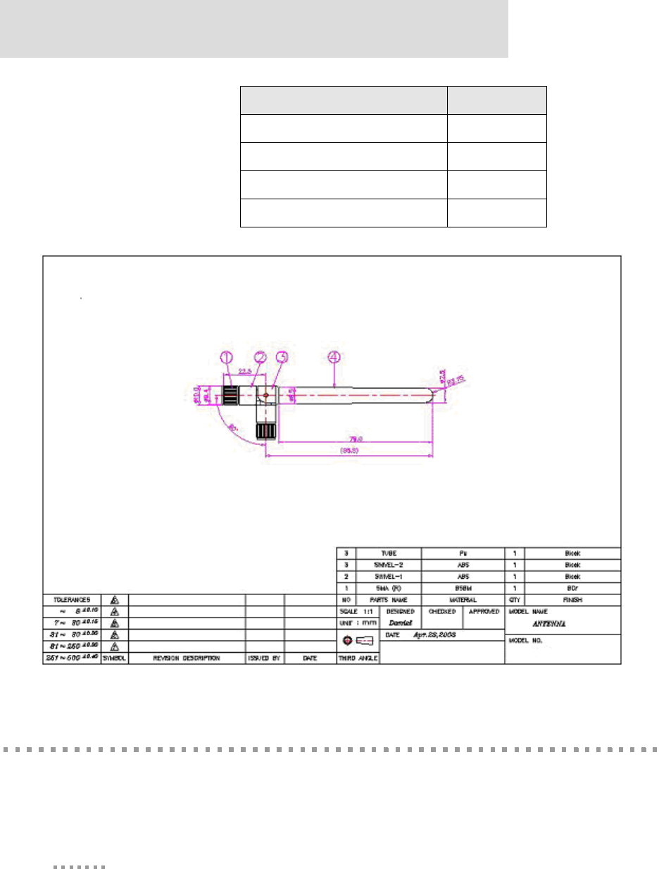
Layouts and Dimensions
The following dimensions and layouts are for both the Digi Connect Wi-EM and Digi
Connect EM. It is strongly recommended that you consider using the Digi Connect Wi-EM
footprint for future flexibility.
Note
All dimensions are in inches. We recommend that you use the Recommended
PCB layout (footprint) of the Digi Connect Wi-EM module regardless of which
module you have. The benefit of using the wireless footprint will allow you to
design your product to go wireless at any time (without difficulty) since the
wireless module is slightly larger.
Module Dimensions
Dimension Digi Connect EM Digi Connect Wi-EM
Length: 1.935 in
(49.149 mm)
1.935 in
(49.149 mm)
Width: 1.575 in
(40.005 mm)
1.855 in
(47.117 mm)
Height:
Fully populated
0.615 in
(15.621 mm)
Pin Header Model
0.262 in
(6.655 mm)
Fully populated
0.575 in
(14.605 mm)
Pin Header Model
0.301 in
(7.645 mm)
49
Specifications
Digi Connect Wi-EM (w/LED Array)
Top
Layouts and Dimensions
50
Digi Connect EM & Wi-EM Hardware Reference
Front
51
Specifications
Bottom
Layouts and Dimensions
52
Digi Connect EM & Wi-EM Hardware Reference
Digi Connect Wi-EM (w/LED Pin Headers)
Top
53
Specifications
Front
Bottom
Layouts and Dimensions
54
Digi Connect EM & Wi-EM Hardware Reference
Digi Connect EM (w/RJ-45 and LED Array)
Top
55
Specifications
Front
Layouts and Dimensions
56
Digi Connect EM & Wi-EM Hardware Reference
Bottom
57
Specifications
Digi Connect EM (with Ethernet and LED Pin Headers)
Top
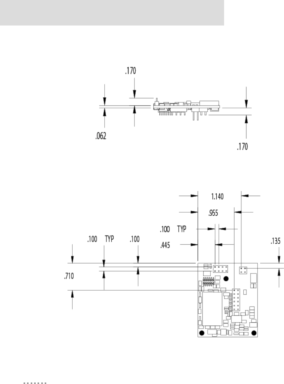
Layouts and Dimensions
58
Digi Connect EM & Wi-EM Hardware Reference
Front
Bottom
59
Specifications
Recommended PCB Layouts
The following graphics are the recommended PCB layouts for the Digi Connect Wi-EM
and Digi Connect EM (both populated and unpopulated versions). It is recommended that
you use the Digi Connect Wi-EM PCB layout for future flexibility since it is slightly wider
than the Digi Connect EM.
Digi Connect Wi-EM (w/LED Array)
Recommended PCB Layouts
60
Digi Connect EM & Wi-EM Hardware Reference
Digi Connect Wi-EM (w/LED Pin Headers)
61
Specifications
Digi Connect EM (w/RJ-45 and LED Array)
Recommended PCB Layouts
62
Digi Connect EM & Wi-EM Hardware Reference
Digi Connect EM (with Ethernet and LED Pin Headers)
63
Specifications
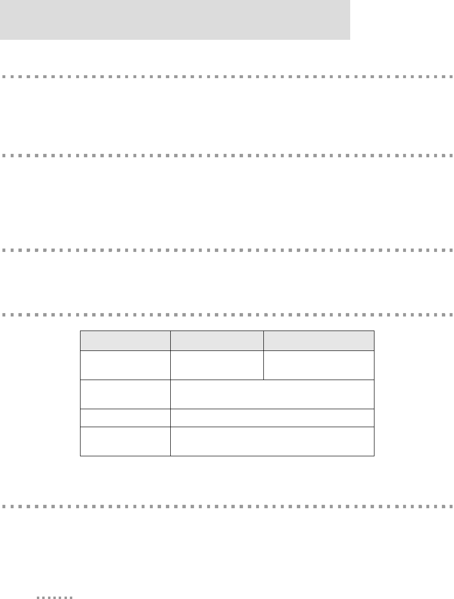
Antenna Information
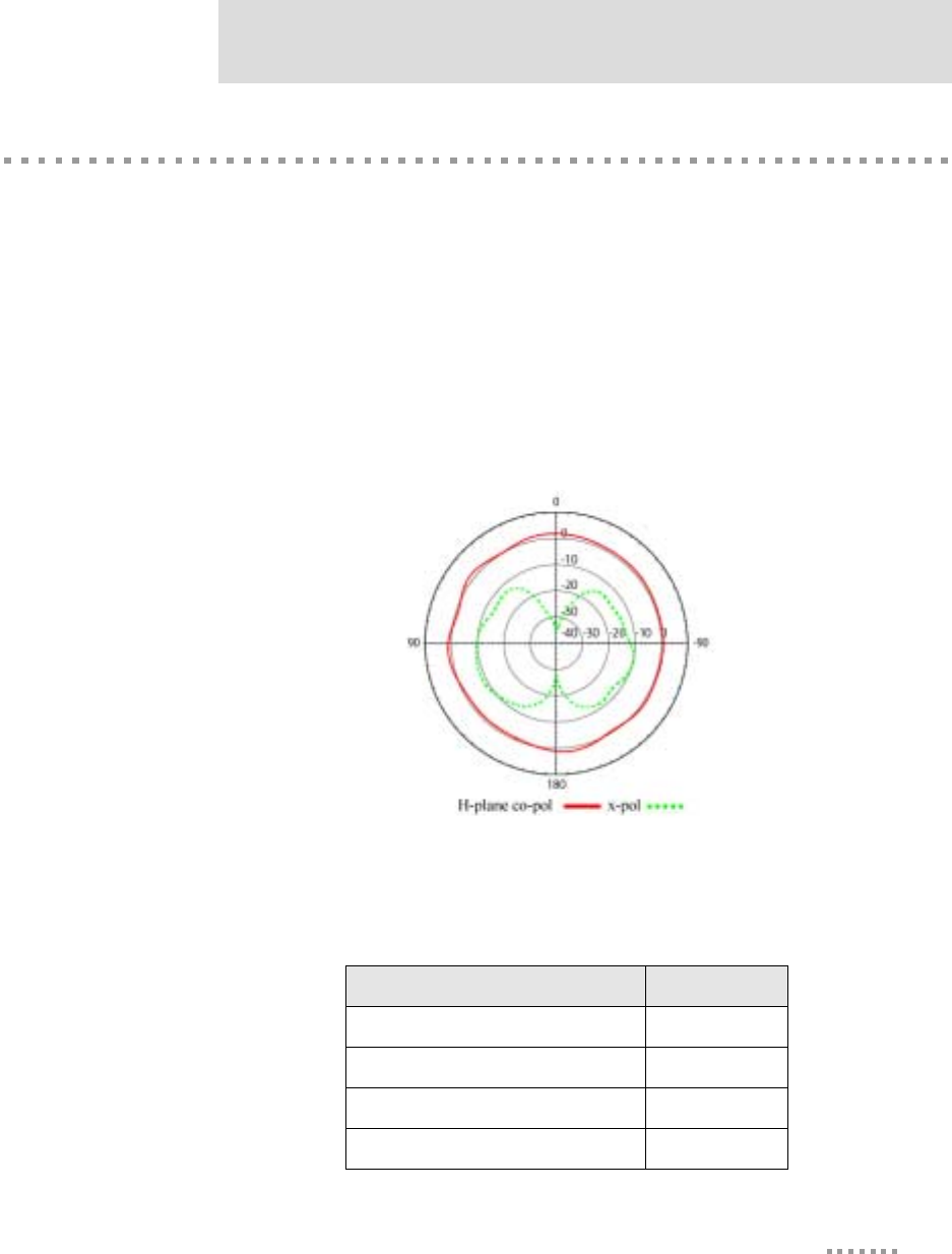
Antenna Strength
The following diagram demonstrates the strength of the signal received by the antenna on
both a horizontal and vertical plane. The diagram shows the magnetic field when the
antenna is in a vertical position. The red line represents the horizontal plane and the dotted
green lined represents the vertical plane. You can see in the illustration that at 90degrees,
the signal strength is (as expected) 0.
Radiation Patterns
Antenna Details
Antenna Description Values
Frequency GHz 2.4~2.5 GHz
Type Dipole
Power Output 2 W
DB Gain 2 dBi
RF Exposure Statement
64
Digi Connect EM & Wi-EM Hardware Reference
RF Exposure Statement
The Digi Connect Wi-EM module complies with the RF exposure limits for humans as
called out in RSS-102. It is exempt from RF evaluation based on its operating frequency of
VSWR < or = 2.0
Dimension 10.0x108.5
Weight 10.5g
Connector RP-SMA
Antenna Description Values

65
Specifications
2.4 GHz, and effective radiated power less than the 3 watt requirement for a mobile device
(>20 cm separation) operating at 2.4 GHz.
Safety Statements
To avoid contact with electrical current:
Never install electrical wiring during an electrical storm.
Never install an ethernet connection in wet locations unless that connector is
specifically designed for wet locations.
Use caution when installing or modifying ethernet lines.
Use a screwdriver and other tools with insulated handles.
You and those around you should wear safety glasses or goggles.
Do not place ethernet wiring or connections in any conduit, outlet or junction
box containing electrical wiring.
Installation of inside wire may bring you close to electrical wire, conduit,
terminals and other electrical facilities. Extreme caution must be used to avoid
electrical shock from such facilities. You must avoid contact with all such
facilities.
Ethernet wiring must be at least 6 feet from bare power wiring or lightning rods
and associated wires, and at least 6 inches from other wire (antenna wires,
doorbell wires, wires from transformers to neon signs), steam or hot water
pipes, and heating ducts.
Do not place an ethernet connection where it would allow a person to use an
ethernet device while in a bathtub, shower, swimming pool, or similar
hazardous location.
Protectors and grounding wire placed by the service provider must not be
connected to, removed, or modified by the customer.
Do not touch uninsulated ethernet wiring if lightning is likely!
Do not touch or move the antenna(s) while the unit is transmitting or receiving.

Safety Statements
66
Digi Connect EM & Wi-EM Hardware Reference
Do not hold any component containing a radio such that the antenna is very
close to or touching any exposed parts of the body, especially the face or eyes,
while transmitting.
Do not operate a portable transmitter near unshielded blasting caps or in an
explosive environment unless it is a type especially qualified for such use
Any external communications wiring you may install needs to be constructed to all
relevant electrical codes. In the United States this is the National Electrical Code Article
800. Contact a licensed electrician for details.

67
Certifications
APPENDIX B
This product complies with the following standards.
FCC Part 15 Class B
Radio Frequency Interference (RFI)(FCC 15.105)
The Digi Connect EM has been tested and found to comply with the limits for Class B
digital devices pursuant to Part 15 Subpart B, of the FCC Rules. These limits are designed
to provide reasonable protection against harmful interference in a residential environment.
This equipment generates, uses, and can radiate radio frequency energy, and if not installed
and used in accordance with the instruction manual, may cause harmful interference to
radio communications. However, there is no guarantee that interference will not occur in a
particular installation. If this equipment does cause harmful interference to radio or
television reception, which can be determined by turning the equipment off and on, the user
is encouraged to try and correct the interference by one or more of the following measures:
Reorient or relocate the receiving antenna.
Increase the separation between the equipment and the receiver.
Connect the equipment into an outlet on a circuit different from that to which
the receiver is connected.
Consult the dealer or an experienced radio/TV technician for help.

Industry Canada
68
Digi Connect EM & Wi-EM Hardware Reference
Labeling Requirements (FCC 15.19)
This device complies with Part 15 of FCC rules. Operation is subject to the following two
conditions: (1) this device may not cause harmful interference, and (2) this device must
accept any interference received, including interference that may cause undesired
operation.
If the FCC ID is not visible when installed inside another device, then the outside of the
device into which the module is installed must also display a label referring to the enclosed
module FCC ID. This exterior label can use wording such as the following: “Contains
Transmitter Module FCC ID: MCQ-50M879” or “Contains FCC ID: MCQ-50M879”.
Modifications (FCC 15.21)
Changes or modifications to this equipment not expressly approved by Digi may void the
user's authority to operate this equipment.
Industry Canada
This digital apparatus does not exceed the Class B limits for radio noise emissions from
digital apparatus set out in the Radio Interference Regulations of the Canadian Department
of Communications.
Le present appareil numerique n'emet pas de bruits radioelectriques depassant les limites
applicables aux appareils numeriques de la class B prescrites dans le Reglement sur le
brouillage radioelectrique edicte par le ministere des Communications du Canada.

69
Certifications
Declaration of Conformity
(In accordance with FCC Dockets 96-208 and 95-19)
Digi International declares, that the products:EM-02T-JT
to which this declaration relates, meet the requirements specified by the Federal
Communications Commission as detailed in the following specifications:
Part 15, Subpart B, for Class B Equipment
FCC Docket 96-208 as it applies to Class B personal
Computers and Peripherals
The products listed above have been tested at an External Test Laboratory certified per
FCC rules and has been found to meet the FCC, Part 15, Class B, Emission Limits.
Documentation is on file and available from the Digi International Homologation
Department.
Manufacturer’s Name: Digi International
Corporate Headquarters: 11001 Bren Road East
Minnetonka MN 55343
Manufacturing Headquarters: 10000 West 76th Street
Eden Prairie MN 55344
Product Name: Digi Connect EM
Model Numbers: 50000873-xx
Product Name: Digi Connect Wi-EM
Model Numbers: 50000879-xx
International EMC Standards
70
Digi Connect EM & Wi-EM Hardware Reference
International EMC Standards
The Digi Connect EM and Digi Connect Wi-Em meet the following electromagnetic
emissions standards:
EN55022
EN55024
EN 300 324
EN 301 489
VCCI
AS 3548
RSS 210 (IC: 1846A-50M879 (Digi Connect Wi-EM)
FCC Part 15 Subpart C (FCC ID: MCQ-50M879 (Digi Connect Wi-EM)
Safety Standards
The embedded modules meet the following safety standards:
UL 60950-1
CSA 22.2 No. 60950
EN60950

71
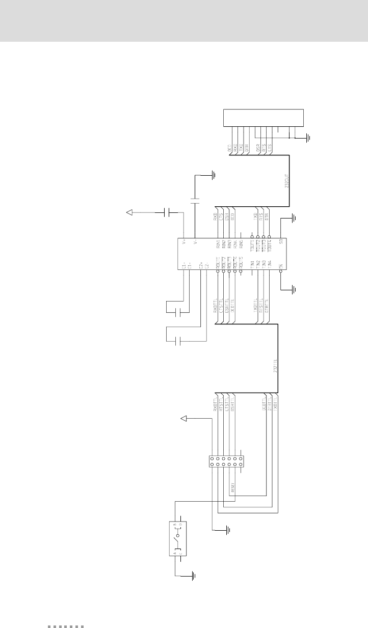
Sample Application:
TTL Signals to EIA-232
APPENDIX C
The following schematic is an example of how to convert the module’s TTL signals to
EIA-232.
72
Digi Connect EM & Wi-EM Hardware Reference
0.1uF
1
2
C6
0.1uF
1
2
C4
0.1uF
1
2
C3
0.1uF
2
1
C5
+5V
GND
11
10
9
8
7
6
5
4
3
2
1
DB9
P1
RS-232 SERIAL 9-PIN CONNECTOR
SHIELD
SHIELD
GND
GND
17
13
25
24
16
15
14
12
28
21
120
36
27
19 18
22 23
26 27
54
89
ADM211E
U1
RS-232 LINE RECVR 5RX 4TX
+5V
GND
1211
109
87
65
43
21
SOCKET 2X6
DIGI ONE EM CONNECTOR
P6
GND GND
RESET SW ITCH
13
24
SW1
Digi International Inc. 2003, 2004. All Rights Reserved.
The Digi logo is a registered trademark of Digi International, Inc.
Connectware, Digi Connect EM and Digi Connect Wi-EM are trademarks of Digi
International, Inc.
NetSilicon, NET+Works, NET+OS, and NET+ are trademarks of NetSilicon, Inc.
All other trademarks mentioned in this document are the property of their respective
owners.