Digi CCIMX6 ConnectCore6 (i.MX6) User Manual Framemaker Book
Digi International Inc ConnectCore6 (i.MX6) Framemaker Book
Digi >
User Manual

ConnectCore 6®
ConnectCore for i.MX6
Preliminary Hardware Reference Manual
90001394

Copyright and Trademarks
© 2014 Digi International Inc. All rights reserved.
Digi, Digi International, the Digi logo, and ConnectCore 6® are trademarks or
registered trademarks in the United States and other countries worldwide. All
other trademarks mentioned in this document are the property of their respective
owners.
Information in this document is subject to change without notice and does not
represent a commitment on the part of Digi International. Digi provides this
document “as is,” without warranty of any kind, expressed or implied, including,
but not limited to, the implied warranties of fitness or merchantability for a
particular purpose. Digi may make improvements and/or changes in this manual
or in the product(s) and/or the program(s) described in this manual at any time.
Contacting Technical Support
Digi International Inc. World Headquarters
11001 Bren Road East Minnetonka, MN 55343
Phone: (866) 765-9885 toll-free U.S.A. & Canada
(801) 765-9885 Worldwide
8:00 am - 5:00 pm (U.S. Mountain Time)
Online Support: www.digi.com/support/
Email: tech.support@digi.com
Fax: 952-912-4952
Revision Record
Revision Date (MM/DD/YY) Description
1P Preliminary draft release

© 2014 Digi International Inc. iii
ConnectCore for i.MX6 Hardware Reference Manual
Table of Contents
Using this Guide. . . . . . . . . . . . . . . . . . . . . . . . . . . . . . . . . . . . . . . . . . . . . . . . . . . . . . .7
Conventions used in this guide . . . . . . . . . . . . . . . . . . . . . . . . . . . . . . . . . . . . . . . . . . . . . .7
Digi Information. . . . . . . . . . . . . . . . . . . . . . . . . . . . . . . . . . . . . . . . . . . . . . . . . . . . . . . . .7
Document Updates . . . . . . . . . . . . . . . . . . . . . . . . . . . . . . . . . . . . . . . . . . . . . . . . . . . .7
Contact Information . . . . . . . . . . . . . . . . . . . . . . . . . . . . . . . . . . . . . . . . . . . . . . . . . . .7
Additional Resources . . . . . . . . . . . . . . . . . . . . . . . . . . . . . . . . . . . . . . . . . . . . . . . . . . .7
About the ConnectCore 6 . . . . . . . . . . . . . . . . . . . . . . . . . . . . . . . . . . . . . . . . . . . . . . .8
ConnectCore 6 Features and Functionality . . . . . . . . . . . . . . . . . . . . . . . . . . . . . . . . . . . . . . . . .8
IEEE 802.11 a/b/g/n and Bluetooth Features and Functionality. . . . . . . . . . . . . . . . . . . . . . . .9
Module Variants . . . . . . . . . . . . . . . . . . . . . . . . . . . . . . . . . . . . . . . . . . . . . . . . . . . . . . . . .9
Block Diagram of the Freescale i.MX6. . . . . . . . . . . . . . . . . . . . . . . . . . . . . . . . . . . . . . . . .10
Power Supply Architecture of the ConnectCore 6. . . . . . . . . . . . . . . . . . . . . . . . . . . . . . . . . 11
Bootstrap . . . . . . . . . . . . . . . . . . . . . . . . . . . . . . . . . . . . . . . . . . . . . . . . . . . . . . . . . . . .14
Module Pinout of the ConnectCore 6 . . . . . . . . . . . . . . . . . . . . . . . . . . . . . . . . . . . . . . . . .15
ConnectCore 6 Pinout Information . . . . . . . . . . . . . . . . . . . . . . . . . . . . . . . . . . . . . . . . . . . 16
Signal Usage Limitations . . . . . . . . . . . . . . . . . . . . . . . . . . . . . . . . . . . . . . . . . . . . . . . . . .52
About the ConnectCore 6 Adapter Board . . . . . . . . . . . . . . . . . . . . . . . . . . . . . . . . . .53
Features of the ConnectCore 6 Adapter Board . . . . . . . . . . . . . . . . . . . . . . . . . . . . . . . . . . . . . .54
ConnectCore 6 Adapter Board . . . . . . . . . . . . . . . . . . . . . . . . . . . . . . . . . . . . . . . . . . . . . .54
ConnectCore 6 GPIO Assignments . . . . . . . . . . . . . . . . . . . . . . . . . . . . . . . . . . . . . . . . . . . 55
I2C Address Table . . . . . . . . . . . . . . . . . . . . . . . . . . . . . . . . . . . . . . . . . . . . . . . . . . . . . .56
I2C2 . . . . . . . . . . . . . . . . . . . . . . . . . . . . . . . . . . . . . . . . . . . . . . . . . . . . . . . . . . . . .56
I2C3 . . . . . . . . . . . . . . . . . . . . . . . . . . . . . . . . . . . . . . . . . . . . . . . . . . . . . . . . . . . . .56
Boot Switches for the ConnectCore 6 . . . . . . . . . . . . . . . . . . . . . . . . . . . . . . . . . . . . . . . . .57
Boot Mode Switch, SW6 . . . . . . . . . . . . . . . . . . . . . . . . . . . . . . . . . . . . . . . . . . . . . . .58
Boot Source Switch, SW5 . . . . . . . . . . . . . . . . . . . . . . . . . . . . . . . . . . . . . . . . . . . . . .58
Configuration Resistors for the ConnectCore 6 . . . . . . . . . . . . . . . . . . . . . . . . . . . . . . . . . .58
Gigabit Ethernet PHY Address . . . . . . . . . . . . . . . . . . . . . . . . . . . . . . . . . . . . . . . . . . . . . .59
USB Host. . . . . . . . . . . . . . . . . . . . . . . . . . . . . . . . . . . . . . . . . . . . . . . . . . . . . . . . . . . . .59
ConnectCore 6 Gigabit LEDs . . . . . . . . . . . . . . . . . . . . . . . . . . . . . . . . . . . . . . . . . . . . . . .59
Gigabit Ethernet LEDs . . . . . . . . . . . . . . . . . . . . . . . . . . . . . . . . . . . . . . . . . . . . . . . . .60
5V Regulator . . . . . . . . . . . . . . . . . . . . . . . . . . . . . . . . . . . . . . . . . . . . . . . . . . . . . . . . . .60
Coin Cell Connector . . . . . . . . . . . . . . . . . . . . . . . . . . . . . . . . . . . . . . . . . . . . . . . . . . . . .61

© 2014 Digi International Inc. iv
ConnectCore for i.MX6 Hardware Reference Manual
Table of Contents
Coin Cell Connector, P5 . . . . . . . . . . . . . . . . . . . . . . . . . . . . . . . . . . . . . . . . . . . . . . . .61
Gigabit Ethernet. . . . . . . . . . . . . . . . . . . . . . . . . . . . . . . . . . . . . . . . . . . . . . . . . . . . . . . .62
Gigabit PHY . . . . . . . . . . . . . . . . . . . . . . . . . . . . . . . . . . . . . . . . . . . . . . . . . . . . . . . . . . .63
Gigabit Connector, J3 . . . . . . . . . . . . . . . . . . . . . . . . . . . . . . . . . . . . . . . . . . . . . . . . . . . .63
HDMI . . . . . . . . . . . . . . . . . . . . . . . . . . . . . . . . . . . . . . . . . . . . . . . . . . . . . . . . . . . . . . .64
HDMI Connector, J22 . . . . . . . . . . . . . . . . . . . . . . . . . . . . . . . . . . . . . . . . . . . . . . . . .64
LVDS1. . . . . . . . . . . . . . . . . . . . . . . . . . . . . . . . . . . . . . . . . . . . . . . . . . . . . . . . . . . . . . .65
LVDS Interface . . . . . . . . . . . . . . . . . . . . . . . . . . . . . . . . . . . . . . . . . . . . . . . . . . . . . .65
LVDS Connector, P7 . . . . . . . . . . . . . . . . . . . . . . . . . . . . . . . . . . . . . . . . . . . . . . . . . .66
MIPI Camera and MIPI Display . . . . . . . . . . . . . . . . . . . . . . . . . . . . . . . . . . . . . . . . . . . . .66
MIPI Connector . . . . . . . . . . . . . . . . . . . . . . . . . . . . . . . . . . . . . . . . . . . . . . . . . . . . .67
PCI Express Mini Card Interface. . . . . . . . . . . . . . . . . . . . . . . . . . . . . . . . . . . . . . . . . . . . .68
PCI Express Mini Card Connector . . . . . . . . . . . . . . . . . . . . . . . . . . . . . . . . . . . . . . . . . . . . 69
Kinetis Microcontroller Assistant, MCA . . . . . . . . . . . . . . . . . . . . . . . . . . . . . . . . . . . . . . . .70
Kinetis MCA Connector, P1 . . . . . . . . . . . . . . . . . . . . . . . . . . . . . . . . . . . . . . . . . . . . . . . .70
Connectors for JSCCWMX53 . . . . . . . . . . . . . . . . . . . . . . . . . . . . . . . . . . . . . . . . . . . . . . . 72
Parallel Camera 0, CSI0 . . . . . . . . . . . . . . . . . . . . . . . . . . . . . . . . . . . . . . . . . . . . . . . . . .72
Parallel Camera 1, CSI1 . . . . . . . . . . . . . . . . . . . . . . . . . . . . . . . . . . . . . . . . . . . . . . . . . .73
LVDS0. . . . . . . . . . . . . . . . . . . . . . . . . . . . . . . . . . . . . . . . . . . . . . . . . . . . . . . . . . . . . . .73
JTAG. . . . . . . . . . . . . . . . . . . . . . . . . . . . . . . . . . . . . . . . . . . . . . . . . . . . . . . . . . . . . . . .74
EIM . . . . . . . . . . . . . . . . . . . . . . . . . . . . . . . . . . . . . . . . . . . . . . . . . . . . . . . . . . . . . . . . 75
Display 0. . . . . . . . . . . . . . . . . . . . . . . . . . . . . . . . . . . . . . . . . . . . . . . . . . . . . . . . . . . . .76
SATA . . . . . . . . . . . . . . . . . . . . . . . . . . . . . . . . . . . . . . . . . . . . . . . . . . . . . . . . . . . . . . .76
Touch . . . . . . . . . . . . . . . . . . . . . . . . . . . . . . . . . . . . . . . . . . . . . . . . . . . . . . . . . . . . . . .77
Keypad . . . . . . . . . . . . . . . . . . . . . . . . . . . . . . . . . . . . . . . . . . . . . . . . . . . . . . . . . . . . . .77
Audio . . . . . . . . . . . . . . . . . . . . . . . . . . . . . . . . . . . . . . . . . . . . . . . . . . . . . . . . . . . . . . .78
PWM. . . . . . . . . . . . . . . . . . . . . . . . . . . . . . . . . . . . . . . . . . . . . . . . . . . . . . . . . . . . . . . . 78
USB Host. . . . . . . . . . . . . . . . . . . . . . . . . . . . . . . . . . . . . . . . . . . . . . . . . . . . . . . . . . . . .79
USB OTG. . . . . . . . . . . . . . . . . . . . . . . . . . . . . . . . . . . . . . . . . . . . . . . . . . . . . . . . . . . . .79
SD2 . . . . . . . . . . . . . . . . . . . . . . . . . . . . . . . . . . . . . . . . . . . . . . . . . . . . . . . . . . . . . . . .79
UART1 . . . . . . . . . . . . . . . . . . . . . . . . . . . . . . . . . . . . . . . . . . . . . . . . . . . . . . . . . . . . . .80
UART2 . . . . . . . . . . . . . . . . . . . . . . . . . . . . . . . . . . . . . . . . . . . . . . . . . . . . . . . . . . . . . .80
CAN1 . . . . . . . . . . . . . . . . . . . . . . . . . . . . . . . . . . . . . . . . . . . . . . . . . . . . . . . . . . . . . . .80

© 2014 Digi International Inc. v
ConnectCore for i.MX6 Hardware Reference Manual
Table of Contents
CAN2 . . . . . . . . . . . . . . . . . . . . . . . . . . . . . . . . . . . . . . . . . . . . . . . . . . . . . . . . . . . . . . .80
ECSPI . . . . . . . . . . . . . . . . . . . . . . . . . . . . . . . . . . . . . . . . . . . . . . . . . . . . . . . . . . . . . . . 81
I2C3 . . . . . . . . . . . . . . . . . . . . . . . . . . . . . . . . . . . . . . . . . . . . . . . . . . . . . . . . . . . . . . . .81
Module Specifications . . . . . . . . . . . . . . . . . . . . . . . . . . . . . . . . . . . . . . . . . . . . . . . . .83
Mechanical specifications . . . . . . . . . . . . . . . . . . . . . . . . . . . . . . . . . . . . . . . . . . . . . . . . .83
Specifications for the ConnectCore 6 . . . . . . . . . . . . . . . . . . . . . . . . . . . . . . . . . . . . . . . . . . . .85
Environmental Specifications . . . . . . . . . . . . . . . . . . . . . . . . . . . . . . . . . . . . . . . . . . . . . . .85
Moisture Sensitivity and Shelf Life . . . . . . . . . . . . . . . . . . . . . . . . . . . . . . . . . . . . . . . . . . . 85
Mounting. . . . . . . . . . . . . . . . . . . . . . . . . . . . . . . . . . . . . . . . . . . . . . . . . . . . . . . . . . . . .85
Solder Paste Print . . . . . . . . . . . . . . . . . . . . . . . . . . . . . . . . . . . . . . . . . . . . . . . . . . . .86
Stencil. . . . . . . . . . . . . . . . . . . . . . . . . . . . . . . . . . . . . . . . . . . . . . . . . . . . . . . . . . . . . . . 86
Coplanarity . . . . . . . . . . . . . . . . . . . . . . . . . . . . . . . . . . . . . . . . . . . . . . . . . . . . . . . . . . .86
SMT Pick and Place . . . . . . . . . . . . . . . . . . . . . . . . . . . . . . . . . . . . . . . . . . . . . . . . . . . . .86
SMT Process Parameter Reference. . . . . . . . . . . . . . . . . . . . . . . . . . . . . . . . . . . . . . . . . . .86
Reflow Profile Using Seven Zone Oven, SAC 305Lead-Free Solder Paste (Alpha OM-340) . . . . 87
Network Interface . . . . . . . . . . . . . . . . . . . . . . . . . . . . . . . . . . . . . . . . . . . . . . . . . . . . . .88
WLAN Standard: . . . . . . . . . . . . . . . . . . . . . . . . . . . . . . . . . . . . . . . . . . . . . . . . . . . . .88
Frequency Band: . . . . . . . . . . . . . . . . . . . . . . . . . . . . . . . . . . . . . . . . . . . . . . . . . . . .88
Data Rates: . . . . . . . . . . . . . . . . . . . . . . . . . . . . . . . . . . . . . . . . . . . . . . . . . . . . . . . .88
Antenna ports: . . . . . . . . . . . . . . . . . . . . . . . . . . . . . . . . . . . . . . . . . . . . . . . . . . . . . .88
Modulation . . . . . . . . . . . . . . . . . . . . . . . . . . . . . . . . . . . . . . . . . . . . . . . . . . . . . . . . . . .89
Security/Interoperability . . . . . . . . . . . . . . . . . . . . . . . . . . . . . . . . . . . . . . . . . . . . . . . . . .89
Frequency Bands . . . . . . . . . . . . . . . . . . . . . . . . . . . . . . . . . . . . . . . . . . . . . . . . . . . . . . .90
US, Canada . . . . . . . . . . . . . . . . . . . . . . . . . . . . . . . . . . . . . . . . . . . . . . . . . . . . . . . .90
Europe. . . . . . . . . . . . . . . . . . . . . . . . . . . . . . . . . . . . . . . . . . . . . . . . . . . . . . . . . . . .90
Australia, New Zealand . . . . . . . . . . . . . . . . . . . . . . . . . . . . . . . . . . . . . . . . . . . . . . . . 90
Japan . . . . . . . . . . . . . . . . . . . . . . . . . . . . . . . . . . . . . . . . . . . . . . . . . . . . . . . . . . . .90
Ad-Hoc Mode Channels . . . . . . . . . . . . . . . . . . . . . . . . . . . . . . . . . . . . . . . . . . . . . . . . 90
5GHz HT20 and HT40 channel available: . . . . . . . . . . . . . . . . . . . . . . . . . . . . . . . . . . . . . . 90
Receive Sensitivity . . . . . . . . . . . . . . . . . . . . . . . . . . . . . . . . . . . . . . . . . . . . . . . . . . . . . .91
Transmit Power . . . . . . . . . . . . . . . . . . . . . . . . . . . . . . . . . . . . . . . . . . . . . . . . . . . . . . . .92
Bluetooth . . . . . . . . . . . . . . . . . . . . . . . . . . . . . . . . . . . . . . . . . . . . . . . . . . . . . . . . . . . .92
Electrical Characteristics . . . . . . . . . . . . . . . . . . . . . . . . . . . . . . . . . . . . . . . . . . . . . . . . . .92

© 2014 Digi International Inc. vi
ConnectCore for i.MX6 Hardware Reference Manual
Table of Contents
Voltage supplies . . . . . . . . . . . . . . . . . . . . . . . . . . . . . . . . . . . . . . . . . . . . . . . . . . . . .92
Power Consumption . . . . . . . . . . . . . . . . . . . . . . . . . . . . . . . . . . . . . . . . . . . . . . . . . . . . . 93
Agency Approval . . . . . . . . . . . . . . . . . . . . . . . . . . . . . . . . . . . . . . . . . . . . . . . . . . . . . . .93
Certifications . . . . . . . . . . . . . . . . . . . . . . . . . . . . . . . . . . . . . . . . . . . . . . . . . . . . . . . .94
Agency Certifications . . . . . . . . . . . . . . . . . . . . . . . . . . . . . . . . . . . . . . . . . . . . . . . . . . . . . . . 94
United States FCC . . . . . . . . . . . . . . . . . . . . . . . . . . . . . . . . . . . . . . . . . . . . . . . . . . . . . .94
FCC Notices . . . . . . . . . . . . . . . . . . . . . . . . . . . . . . . . . . . . . . . . . . . . . . . . . . . . . . . .94
FCC-Approved Antennas . . . . . . . . . . . . . . . . . . . . . . . . . . . . . . . . . . . . . . . . . . . . . . . 95
Antennas Approved for Use with the ConnectCore™ for i.MX6 Wi-Fi Modules . . . . . . . . . .95
. . . . . . . . . . . . . . . . . . . . . . . . . . . . . . . . . . . . . . . . . . . . . . . . . . . . . . . . . . . . . . . . .95
RF Exposure. . . . . . . . . . . . . . . . . . . . . . . . . . . . . . . . . . . . . . . . . . . . . . . . . . . . . . . .96
Europe (ETSI) . . . . . . . . . . . . . . . . . . . . . . . . . . . . . . . . . . . . . . . . . . . . . . . . . . . . . . . . .96
OEM Labeling Requirements . . . . . . . . . . . . . . . . . . . . . . . . . . . . . . . . . . . . . . . . . . . . 96
CE Labeling Requirements . . . . . . . . . . . . . . . . . . . . . . . . . . . . . . . . . . . . . . . . . . . . . .96
Declarations of Conformity. . . . . . . . . . . . . . . . . . . . . . . . . . . . . . . . . . . . . . . . . . . . . . 97
Approved Antennas. . . . . . . . . . . . . . . . . . . . . . . . . . . . . . . . . . . . . . . . . . . . . . . . . . .97
Canada (IC). . . . . . . . . . . . . . . . . . . . . . . . . . . . . . . . . . . . . . . . . . . . . . . . . . . . . . . . . . .97
Labeling Requirements . . . . . . . . . . . . . . . . . . . . . . . . . . . . . . . . . . . . . . . . . . . . . . . . 97
Transmitters with Detachable Antennas . . . . . . . . . . . . . . . . . . . . . . . . . . . . . . . . . . . . 97
Japan . . . . . . . . . . . . . . . . . . . . . . . . . . . . . . . . . . . . . . . . . . . . . . . . . . . . . . . . . . . . . . . 98

© 2014 Digi International Inc. 7
ConnectCore for i.MX6 Hardware Reference Manual
Using this Guide
This guide provides information about the Digi ConnectCore for i.MX6 embedded core module
family.
Conventions used in this guide
This table describes the typographic conventions used in this guide:
Digi Information
Document Updates
Please always check the product specific section on the Digi support website at
www.digiembedded.com/support
for the most current revision of this document.
Contact Information
For more information about your Digi products, or for customer service and technical support,
contact Digi International.
Additional Resources
Refer to the most recent Freescale i.MX6 processor reference manual and related documentation
(available on the Freescale web site at: http://www.freescale.com/imx6) for additional
information.
This convention Is used for
italic
type
Emphasis, new terms, variables, and document titles.
monospaced type
Filenames, pathnames, and code examples.
To contact Digi International by Use
Mail
Digi International
1101 Bren Road East
Minnetonka, MN 55343
U.S.A.
World Wide Web http://www.digiembedded.com/support/
Telephone (U.S.) (952) 912-3444 or (877) 912-3444
Telephone (other locations) +1 (952) 912-3444 or (877) 912-3444

© 2014 Digi International Inc. 8
ConnectCore for i.MX6 Hardware Reference Manual
About the ConnectCore 6
The ConnectCore 6 is an ultra-compact and highly integrated system-on-module solution based
on the Freescale i.MX6 Cortex-A9 processor family.
With processor speeds up to 1.2 GHz and fully interchangeable single-/dual-/quad-core variants,
the ConnectCore 6 offers a truly future-proof platform solution with scalable performance and
pre-certified wireless 802.11a/b/g/n and Bluetooth 4.0, including Bluetooth Low Energy
connectivity.
Its innovative and scalable design maximizes integration flexibility and significantly reduces
design risk in a highly cost-effective, reliable, low-profile surface mount form factor with optimal
thermal management even in the most demanding quad-core system configurations.
Seamless Cloud Connector integration as part of the Digi Linux and Android software platform
support offers secure remote management and web services capabilities through the scalable
Device Cloud™ by Etherios™.
In addition, Digi offers complete professional Etherios custom hardware and wireless design
services as well as end-to-end solutions services for cloud integration and app development.
ConnectCore 6 Features and Functionality
The ConnectCore for i.MX6 module is based on the i.MX6 processor from Freescale. This
processor offers a high number of interfaces. Most of these interfaces are multiplexed and are
not available simultaneously. The module has the following features:
• i.MX6 single/dual/quad ARM Cortex-A9 cores operating at speeds up to 1.2GHz.
• 32Kbytes L1 Instruction cache
• 32Kbytes L1 Data cache
• Up to 1MB unified Instruction/Data L2 cache
• NEON MPE (Media Processing Engine) co-processor
• Graphical Hardware accelerators:
• IPU (Image Processing Unit)
• Optional VPU (Video Processing Unit)
• Optional 2D/3D GPU (Graphics Processing Unit)
• 64-bit DDR3-1066 memory interface with a density up to 2GBytes.
• 8-bit eMMC support up to revision 4.4/4.41
• Dialog DA9063 Power Management IC (PMIC)
• 6x DC/DC buck converters
• 11x LDO regulators
• RTC with rechargeable coin cell battery support
• 10-bit ADC channels
• GPIO pins
• Optional IEEE802.11a/b/g/n WLAN interface with spatial diversity support.
• SoftAP (Software Access Point) support
• Optional Bluetooth 4.0 dual mode
• Optional Cortex-M0+/Cortex-M4 MCA (Microcontroller Assist) subsystem
• Debug interfaces:
• Standard JTAG controller IEEE 1149.1

© 2014 Digi International Inc. 9
ConnectCore for i.MX6 Hardware Reference Manual
• ETM/ETB support
• Support of i.MX6 typical interfaces:
• 16/32-bit data/address bus
• SATA II, 3.0Gbps (24-bit parallel bus, LVDS, HDMI, MIPI/DSI)
• Cameras (20-bit parallel bus, MIPI/CSI)
• MMC/SD/SDIO
• 1x USB OTG with integrated PHY
• 3x USB Host
• 1x Host with integrated PHY
• 2x Host with integrated HS-IC USB PHY
• PCI Express Gen 2.0 lane
• Gigabit Ethernet MAC
• 10/100M Ethernet MAC
• UART, SPI, I2C, PWM, CAN, I2S and GPIO
• Ultra-miniature SMT module (50x50mmx5mm) based on 400-LGA pads
IEEE 802.11 a/b/g/n and Bluetooth Features and Functionality
The RF interface of the ConnectCore for i.MX6 is handled by a Qualcomm-Atheros module
capable of 2.4 GHz and 5 GHz connections using 802.11 a/b/g/n and Bluetooth 4.0 (Dual mode
with Blueooth Low Energy support).
The module is built with coexistence in mind and handles the BT coexistence internally. Cellular
coexistence filtering is onboard to aid in designing systems susceptible to cellular interference.
Module Variants
The ConnectCore for i.MX6 module supports population options such as network interface
(Wi-Fi), memory (flash, RAM), MCU-assist, processor (single, dual and quad-cores), and others.
© 2014 Digi International Inc. 10
ConnectCore for i.MX6 Hardware Reference Manual
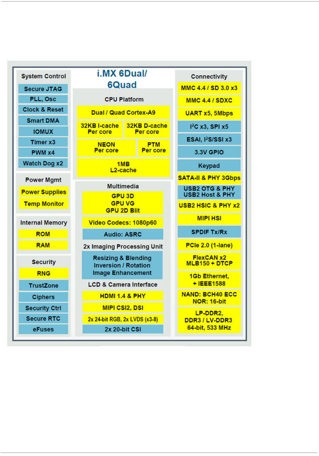
Block Diagram of the Freescale i.MX6
The figure below shows the block diagram of the Freescale i.MX6 application processor. Not all
functions are available on all processor variants.
Block diagram of the ConnectCore 6 CPU
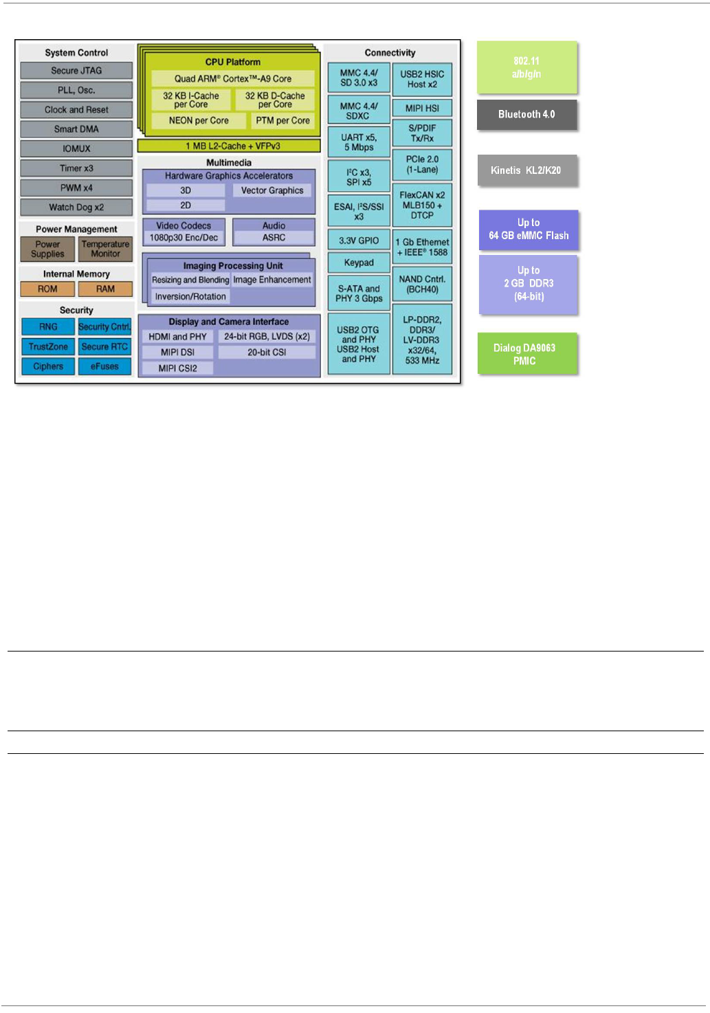
The following figure below provides a high-level block diagram of the ConnectCore for i.MX6
module.
© 2014 Digi International Inc. 11
ConnectCore for i.MX6 Hardware Reference Manual
Block diagram of ConnectCore 6
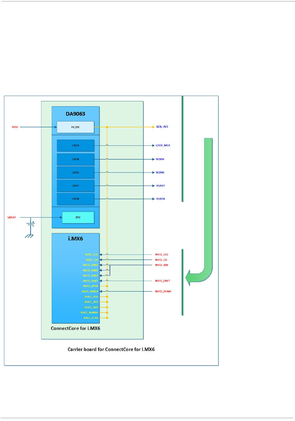
Power Supply Architecture of the ConnectCore 6
The ConnectCore for i.MX6 provides a primary 5V power supply input. This supply is the main
power domain to the on-module Dialog DA9063 power management IC (PMIC), which generates
all required supply voltages for the module components as well as the carrier board.
The module provides support for a backup battery (coin-cell or super cap) powering the real-
time clock (RTC) on the module. In addition, rechargeable backup batteries (ML414, others) are
also supported.
The PMIC generates the following power domains that are available on the module pads:
• 3.3V (GEN_3V3)
Note: The maximum current consumption mentioned above is a combination of the current
consumed by the module and by the carrier board.
Moreover, 5x PMIC LDO outputs are also available on the module pads:
• VLDO3
• VLDO4
• VLDO6
• VLDO7
• VLDO8
Power
domain
Regulator
type
Output
accuracy
Maximum
current
Dropout voltage
(MAX)
Turn on time
(MAX)
Turn off
time
(MAX)
Quiescent
current in
OFF mode
(TYP)
3.3V DC/DC +/-3% 1500mA - 1µA 1.2ms -

© 2014 Digi International Inc. 12
ConnectCore for i.MX6 Hardware Reference Manual
The table below provides the characteristics of the optional LDO outputs:
Note:
• For information about using the LDOs options, please contact Digi.
• VLDO3 is used for supplying MCA processor on the module.
The power management IC located on the module is responsible for generating all required
i.MX6 processor supply voltages. The following i.MX6x supplies are available on the module
pads:
• NVCC_ENET
• NVCC_EIM
• NVCC_LCD
• NVCC_CSI
• NVCC_RGMII
Some of the I/O supplies are set on the module. See the table following table:
The remaining I/O voltages must be set externally and are left open on the ConnectCore for
i.MX6 module. See the following table for operating ranges of the remaining I/O supplies.
LDO Output
voltage
Output
accuracy
Default
voltage
Maximum
current
Dropout voltage
(MAX)
Turn on time
(MAX)
Turn
off
time
(MAX)
Quiescent
current in
OFF mode
(TYP)
VLDO3 0.9-3.44V +/-3% 3.3V 200mA 150mV 1µA 300µs 1ms
VLDO4 0.9-3.44V +/-3% 3.3V 200mA 150mV 1µA 300µs 1ms
VLDO6 0.9-3.6V +/-3% 3.3V 200mA 150mV 1µA 200µs 1ms
VLDO7 0.9-3.6V +/-3% 1.8V 200mA 150mV 1µA 300µs 1ms
VLDO8 0.9-3.6V +/-3% 3.3V 200mA 150mV 1µA 300µs 1ms
Power domain Connection
NVCC_GPIO GEN_3V3
NVCC_JTAG GEN_3V3
NVCC_NANDF GEN_3V3
NVCC_SD1 GEN_3V3
NVCC_SD2 GEN_3V3
NVCC_SD3 GEN_3V3
Power domain Min Type Max
NVCC_ENET 1.65V 1.8V 3.6V
NVCC_EIM 2.8V
NVCC_LCD 3.3V
NVCC_CSI -
NVCC_RGMII in HSIC 1.2V mode 1.15V - 1.30V
NVCC_RGMII in RGMII 1.5V mode 1.43V - 1.58V
NVCC_ 1.8V mode 1.70V - 1.90V
NVCC_RGMII in RGMII 2.5V mode 2.25V - 2.625V
© 2014 Digi International Inc. 13
ConnectCore for i.MX6 Hardware Reference Manual
As shown in the table above, the supplies have a wide operating range. In order to provide the
most cost-effective and flexible solution for a given use-case, the supplies listed in the table need
to be provided by the carrier board integrating the ConnectCore for i.MX6 module. However,
PMIC power domains 3.3V - and LDO3/4/6/7/8 options - are dedicated power sources for
supplying i.MX6 power domains.
The MCU - assist specific power domain (LDO3_MCA) available on the ConnectCore for i.MX6
LGA pads is a power supply output powering the on-module Kinetis processor.
The following diagram outlines the power supply approach of the ConnectCore for i.MX6. Inputs
are marked red, blue marks outputs.
ConnectCore 6 power supply diagram

© 2014 Digi International Inc. 14
ConnectCore for i.MX6 Hardware Reference Manual
Bootstrap
The ConnectCore 6 is configured by default to boot in “Internal boot” mode. See the following
table:
Note:
• 10K pull-up populated on BOOT_MODE1
• 10K pull-down populated on BOOT_MODE0
By default, the boot media configured on the ConnectCore for i.MX6 module is the on-module
eMMC. This is achieved by having the following resistors populated on the module:
• 10K pull-down on EIM_DA4 (BOOT_CFG1[4])
• 10K pull-up on EIM_DA5 (BOOT_CFG1[5])
• 10K pull-up on EIM_DA5 (BOOT_CFG1[6])
• 10K pull-up on EIM_DA7 (BOOT_CFG1[7]
• 10K pull-down on EIM_DA11 (BOOT_CFG2[3])
• 10K pull-up on EIM_DA12 (BOOT_CFG2[4])
When selecting “Internal Boot”, bootstrap pins shall be protected to insure a proper boot
process. “Internal Boot” has the benefit that multiple boot media can be supported. For mass
production, Digi recommends to use “Boot from fuses” for more security.
BOOT_MODE [1:0] Boot type
00 Boot from fuses
01 Serial Downloader
10 Internal Boot (default)
11 Reserved
© 2014 Digi International Inc. 15
ConnectCore for i.MX6 Hardware Reference Manual
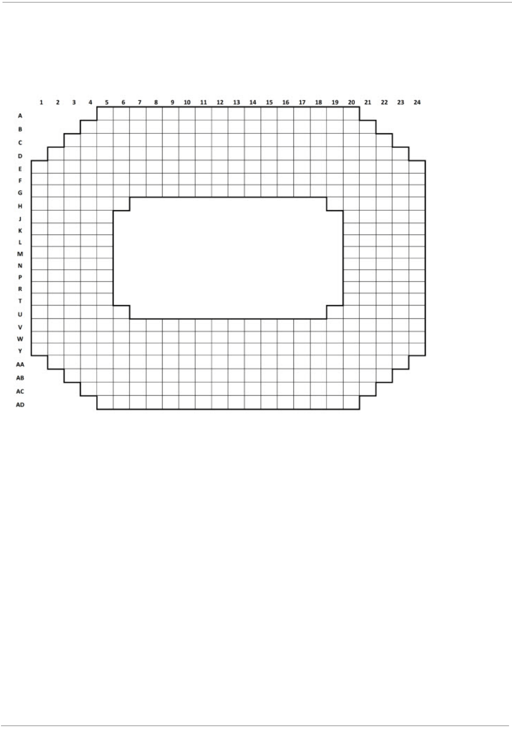
Module Pinout of the ConnectCore 6
The module has a LGA pad structure based on 400 pads. See the following diagram for the
general layout.
ConnectCore top view module pinout

© 2014 Digi International Inc. 16
ConnectCore for i.MX6 Hardware Reference Manual
ConnectCore 6 Pinout Information
The following table provides pinout information of the ConnectCore for i.MX6 module.
Please also refer to the Freescale i.MX6 technical documentation for additional information
related to the signals listed in the table.
LGA pad Pad name Multiplexing IO type Comments
A5 CSI0_MCLK
ALT0: IPU1_CSI0_HSYNC
ALT1:
ALT2:
ALT3: CCM_CLKO1
ALT4:
ALT5: GPIO5_IO19
ALT6:
ALT: ARM_TRACE_CTL
NVCC_CSI
A6 CSI0_DAT11
ALT0: IPU1_CSI0_DATA11
ALT1: AUD3_RXFS
ALT2: ECSPI2_SS0
ALT3: UART1_RX_DATA
ALT4:
ALT5: GPIO5_IO29
ALT6:
ALT7: ARM_TRACE08
NVCC_CSI Connected on module
to MCA processor
A7 CSI0_DAT17
ALT0: IPU1_CSI0_DATA17
ALT1: EIM_DATA13
ALT2:
ALT3: UART4_CTS_B
ALT4:
ALT5: GPIO6_IO03
ALT6:
ALT7: ARM_TRACE14
NVCC_CSI
A8 GND -
A9 HDMI_D0_N HDMI_VPH
A10 GND -
A11 CSI_CLK0_P NVCC_MIPI
A12 GND -
A13 CSI_D1_N NVCC_MIPI
A14 PCIE_RX_N PCIE_VPH
A15 PCIE_TX_N PCIE_VPH
A16 CLK2_P VDD_HIGH_CAP
A17 GND -
A18 CLK1_P VDD_HIGH_CAP
A19 MLB_DP VDD_HIGH_CAP
A20 MLB_DN VDD_HIGH_CAP
B4 LVDS0_TX2_P NVCC_LVDS_2P5
B5 GND -

© 2014 Digi International Inc. 17
ConnectCore for i.MX6 Hardware Reference Manual
B6 CSI0_DAT14
ALT0: IPU1_CSI0_DATA14
ALT1: EIM_DATA10
ALT2:
ALT3: UART5_TX_DATA
ALT4:
ALT5: GPIO6_IO00
ALT6:
ALT7: ARM_TRACE11
NVCC_CSI
B7 CSI0_DAT4
ALT0: IPU1_CSI0_DATA04
ALT1: EIM_DATA02
ALT2: ECSPI1_SCLK
ALT3: KEY_COL5
ALT4: AUD3_TXC
ALT5: GPIO5_IO22
ALT6:
ALT7: ARM_TRACE01
NVCC_CSI
B8 HDMI_D1_N HDMI_VPH
B9 HDMI_D0_P HDMI_VPH
B10 DSI_D0_P NVCC_MIPI
B11 CSI_CLK0_N NVCC_MIPI
B12 CSI_D2_N NVCC_MIPI
B13 CSI_D1_P NVCC_MIPI
B14 PCIE_RX_P PCIE_VPH
B15 PCIE_TX_P PCIE_VPH
B16 CLK2_N VDD_HIGH_CAP
B17 GND -
B18 CLK1_N VDD_HIGH_CAP
B19 GND -
B20 GND -
B21 SD3_CLK/
BT_UART_RTS
ALT0: SD3_CLK
ALT1: UART2_RTS_B
ALT2: FLEXCAN1_RX
ALT3:
ALT4:
ALT5: GPIO7_IO03
ALT6:
ALT7:
NVCC_SD3
(GEN_3V3)
Connected to
Bluetooth module
C3 KEY_COL3
ALT0: ECSPI1_SS3
ALT1: ENET_CRS
ALT2: HDMI_TX_DDC_SCL
ALT3: KEY_COL3
ALT4: I2C2_SCL
ALT5: GPIO4_IO12
ALT6: SPDIF_IN
ALT7:
NVCC_GPIO
(GEN_3V3)
Connected to MCA
processor and PMIC.
Not recommended as
main I2C port.
4,7K pull-up on
module.
C4 LVDS0_TX2_N NVCC_LVDS_2P5

© 2014 Digi International Inc. 18
ConnectCore for i.MX6 Hardware Reference Manual
C5 CSI0_DAT6
ALT0: IPU1_CSI0_DATA06
ALT1: EIM_DATA04
ALT2: ECSPI1_MISO
ALT3: KEY_COL6
ALT4: AUD3_TXFS
ALT5: GPIO5_IO24
ALT6:
ALT7: ARM_TRACE03
NVCC_CSI
C6 CSI0_DAT13
ALT0: IPU1_CSI0_DATA13
ALT1: EIM_DATA09
ALT2:
ALT3: UART4_RX_DATA
ALT4:
ALT5: GPIO5_IO31
ALT6:
ALT7: ARM_TRACE10
NVCC_CSI
C7 CSI0_DAT5
ALT0: IPU1_CSI0_DATA05
ALT1: EIM_DATA03
ALT2: ECSPI1_MOSI
ALT3: KEY_ROW5
ALT4: AUD3_TXD
ALT5: GPIO5_IO23
ALT6:
ALT7: ARM_TRACE02
NVCC_CSI
C8 HDMI_D1_P HDMI_VPH
C9 GND -
C10 DSI_D0_N NVCC_MIPI
C11 GND -
C12 CSI_D2_P NVCC_MIPI
C13 GND -
C14 GND -
C15 GND -
C16 USB_H1_DN VDD_USB_CAP
C17 TAMPER VDD_SNVS_IN
C18 Reserved -
C19 MLB_SP VDD_HIGH_CAP
C20 MLB_SN VDD_HIGH_CAP
C21 SD3_DAT7
ALT0: SD3_DATA7
ALT1: UART1_TX_DATA
ALT2:
ALT3:
ALT4:
ALT5: GPIO6_IO17
ALT6:
ALT7:
NVCC_SD3
(GEN_3V3)

© 2014 Digi International Inc. 19
ConnectCore for i.MX6 Hardware Reference Manual
C22 SD3_DAT4/
BT_UART_RXD
ALT0: SD3_DATA4
ALT1: UART2_RX_DATA
ALT2:
ALT3:
ALT4:
ALT5: GPIO7_IO01
ALT6:
ALT7:
NVCC_SD3
(GEN_3V3)
Connected to
Bluetooth module
D2 KEY_ROW4
ALT0: FLEXCAN2_RX
ALT1: IPU1_SISG5
ALT2: USB_OTG_PWR
ALT3: KEY_ROW4
ALT4: UART5_CTS_B
ALT5: GPIO4_IO15
ALT6:
ALT7:
NVCC_GPIO
(GEN_3V3)
D3 KEY_ROW1
ALT0: ECSPI1_SS0
ALT1: ENET_COL
ALT2: AUD5_RXD
ALT3: KEY_ROW1
ALT4: UART5_RX_DATA
ALT5: GPIO4_IO09
ALT6: SD2_VSELECT
ALT7:
NVCC_GPIO
(GEN_3V3)
D4 GND -
D5 CSI0_DAT9
ALT0: IPU1_CSI0_DATA09
ALT1: EIM_DATA07
ALT2: ECSPI2_MOSI
ALT3: KEY_ROW7
ALT4: I2C1_SCL
ALT5: GPIO5_IO27
ALT6:
ALT7: ARM_TRACE06
NVCC_CSI Connected on module
to MCA processor
D6 CSI0_DAT8
ALT0: IPU1_CSI0_DATA08
ALT1: EIM_DATA06
ALT2: ECSPI2_SCLK
ALT3: KEY_COL7
ALT4: I2C1_SDA
ALT5: GPIO5_IO26
ALT6:
ALT7: ARM_TRACE05
NVCC_CSI Connected on module
to MCA processor
D7 HDMI_DDCCEC HDMI_VPH
D8 GND -
D9 DSI_D1_P NVCC_MIPI
D10 GND -
D11 CSI_D3_P NVCC_MIPI
D12 Reserved -
D13 #BT_DISABLE WLAN/BT_3V3
D14 JTAG_TDI NVCC_JTAG
(GEN_3V3)

© 2014 Digi International Inc. 20
ConnectCore for i.MX6 Hardware Reference Manual
D15 #JTAG_TRST NVCC_JTAG
(GEN_3V3)
D16 USB_H1_DP VDD_USB_CAP
D17 TEST_MODE VDD_SNVS_IN
D18 ON/OFF VDD_SNVS_IN Must be connected to a
power button
D19 SATA_TX_N SATA_VPH
D20 GND -
D21 SD3_DAT1
ALT0: SD3_DATA1
ALT1: UART1_RTS_B
ALT2: FLEXCAN2_RX
ALT3:
ALT4:
ALT5: GPIO7_IO05
ALT6:
ALT7:
NVCC_SD3
(GEN_3V3)
D22 SD3_RST
ALT0: SD3_RESET
ALT1: UART3_RTS_B
ALT2:
ALT3:
ALT4:
ALT5: GPIO7_IO08
ALT6:
ALT7:
NVCC_SD3
(GEN_3V3)
D23 SD3_DAT5/
BT_UART_TXD
ALT0: SD3_DATA5
ALT1: UART2_TX_DATA
ALT2:
ALT3:
ALT4:
ALT5: GPIO7_IO00
ALT6:
ALT7:
NVCC_SD3
(GEN_3V3)
Connected to
Bluetooth module
E1 LVDS1_CLK_N NVCC_LVDS_2P5
E2 KEY_ROW0
ALT0: ECSPI1_MOSI
ALT1: ENET_TX_DATA3
ALT2: AUD5_TXD
ALT3: KEY_ROW0
ALT4: UART4_RX_DATA
ALT5: GPIO4_IO07
ALT6: DCIC2_OUT
ALT7:
NVCC_GPIO
(GEN_3V3)
E3 KEY_COL1
ALT0: ECSPI1_MISO
ALT1: ENET_MDIO
ALT2: AUD5_TXFS
ALT3: KEY_COL1
ALT4: UART5_TX_DATA
ALT5: GPIO4_IO08
ALT6: SD1_VSELECT
ALT7:
NVCC_GPIO
(GEN_3V3)
E4 LVDS0_TX1_P NVCC_LVDS_2P5

© 2014 Digi International Inc. 21
ConnectCore for i.MX6 Hardware Reference Manual
E5 CSI0_DATA_EN
ALT0: IPU1_CSI0_DATA_EN
ALT1: EIM_DATA00
ALT2:
ALT3:
ALT4:
ALT5: GPIO5_IO20
ALT6:
ALT7: ARM_TRACE_CLK
NVCC_CSI
E6 CSI0_DAT15
ALT0: IPU1_CSI0_DATA15
ALT1: EIM_DATA11
ALT2:
ALT3: UART5_RX_DATA
ALT4:
ALT5: GPIO6_IO01
ALT6:
ALT7: ARM_TRACE12
NVCC_CSI
E7 GND -
E8 HDMI_CLK_N HDMI_VPH
E9 DSI_D1_N NVCC_MIPI
E10 DSI_CLK0_N NVCC_MIPI
E11 CSI_D3_N NVCC_MIPI
E12 Reserved -
E13 Reserved -
E14 JTAG_TDO NVCC_JTAG
(GEN_3V3)
E15 Reserved -
E16 GND -
E17 BOOT_MODE0 VDD_SNVS_IN
E18 #POR VDD_SNVS_IN
E19 SATA_TX_P SATA_VPH
E20 GEN_3V3 NVCC_SD3
(GEN_3V3
E21 SD3_DAT6
ALT0: SD3_DATA6
ALT1: UART1_RX_DATA
ALT2:
ALT3:
ALT4:
ALT5: GPIO6_IO18
ALT6:
ALT7:
NVCC_SD3
(GEN_3V3)
E22 NANDF_CLE/
BT_WAKE
ALT0: NAND_CLE
ALT1: IPU2_SISG4
ALT2:
ALT3:
ALT4:
ALT5: GPIO6_IO07
ALT6:
ALT7:
NVCC_NANDF
(GEN_3V3)

© 2014 Digi International Inc. 22
ConnectCore for i.MX6 Hardware Reference Manual
E23 SD3_CMD/
BT_UART_CTS
ALT0: SD3_CMD
ALT1: UART2_CTS_B
ALT2: FLEXCAN1_TX
ALT3:
ALT4:
ALT5: GPIO7_IO02
ALT6:
ALT7:
NVCC_SD3
(GEN_3V3)
E24 SD3_DAT2
ALT0: SD3_DATA2
ALT1:
ALT2:
ALT3:
ALT4:
ALT5: GPIO7_IO06
ALT6:
ALT7:
NVCC_SD3
(GEN_3V3)
F1 LVDS1_CLK_P NVCC_LVDS_2P5
F2 KEY_ROW3
ALT0:
ALT1: ASRC_EXT_CLK
ALT2: HDMI_TX_DDC_SDA
ALT3: KEY_ROW3
ALT4: I2C2_SDA
ALT5: GPIO4_IO13
ALT6: SD1_VSELECT
ALT7:
NVCC_GPIO
(GEN_3V3)
Connected to MCA
processor and PMIC.
Not recommended as
main I2C port. 4,7K
pull-up on module.
F3 GPIO_8
ALT0: ESAI_TX5_RX0
ALT1: XTALOSC_REF_CLK_32K
ALT2: EPIT2_OUT
ALT3: FLEXCAN1_RX
ALT4: UART2_RX_DATA
ALT5: GPIO1_IO08
ALT6: SPDIF_SR_CLK
ALT7: USB_OTG_PWR_CTL_WAKE
NVCC_GPIO
(GEN_3V3)
F4 LVDS0_TX1_N NVCC_LVDS_2P5
F5 GND -
F6 CSI0_DAT18
ALT0: IPU1_CSI0_DATA18
ALT1: EIM_DATA14
ALT2:
ALT3: UART5_RTS_B
ALT4:
ALT5: GPIO6_IO04
ALT6:
ALT7: ARM_TRACE15
NVCC_CSI
F7 HDMI_D2_N HDMI_VPH
F8 HDMI_CLK_P HDMI_VPH
F9 GND -
F10 DSI_CLK0_P NVCC_MIPI
F11 GND -
F12 GND -
F13 JTAG_TCK NVCC_JTAG
(GEN_3V3)

© 2014 Digi International Inc. 23
ConnectCore for i.MX6 Hardware Reference Manual
F14 JTAG_TMS NVCC_JTAG
(GEN_3V3)
F15 BOOT_MODE1 VDD_SNVS_IN
F16 USB_H1_VBUS -
F17 MLB_CP -
F18 MLB_CN -
F19 GND -
F20 SD3_DAT0
ALT0: SD3_DATA0
ALT1: UART1_CTS_B
ALT2: FLEXCAN2_TX
ALT3:
ALT4:
ALT5: GPIO7_IO04
ALT6:
ALT7:
NVCC_SD3
(GEN_3V3)
F21 NANDF_CS0
ALT0: NAND_CE0_B
ALT1:
ALT2:
ALT3:
ALT4:
ALT5: GPIO6_IO11
ALT6:
ALT7:
NVCC_NANDF
(GEN_3V3)
F22 #NANDF_WP
ALT0: NAND_WP_B
ALT1: IPU2_SISG5
ALT2:
ALT3:
ALT4:
ALT5: GPIO6_IO09
ALT6:
ALT7:
NVCC_NANDF
(GEN_3V3)
F23 NANDF_CS3
ALT0: NAND_CE3_B
ALT1: IPU1_SISG1
ALT2: ESAI_TX1
ALT3: EIM_ADDR26
ALT4:
ALT5: GPIO6_IO16
ALT6: IPU2_SISG1
ALT7:
NVCC_NANDF
(GEN_3V3)
F24 SD3_DAT3
ALT0: SD3_DATA3
ALT1: UART3_CTS_B
ALT2:
ALT3:
ALT4:
ALT5: GPIO7_IO07
ALT6:
ALT7:
NVCC_SD3
(GEN_3V3)
G1 GND -

© 2014 Digi International Inc. 24
ConnectCore for i.MX6 Hardware Reference Manual
G2 GPIO_0
ALT0: CCM_CLKO1
ALT1:
ALT2: KEY_COL5
ALT3: ASRC_EXT_CLK
ALT4: EPIT1_OUT
ALT5: GPIO1_IO00
ALT6: USB_H1_PWR
ALT7: SNVS_VIO_5
NVCC_GPIO
(GEN_3V3)
G3 GPIO_2
ALT0: ESAI_TX_FS
ALT1:
ALT2: KEY_ROW6
ALT3:
ALT4:
ALT5: GPIO1_IO02
ALT6: SD2_WP
ALT7: MLB_DATA
NVCC_GPIO
(GEN_3V3)
G4 GND -
G5 CSI0_PIXCLK
ALT0: IPU1_CSI0_PIXCLK
ALT1:
ALT2:
ALT3:
ALT4:
ALT5: GPIO5_IO18
ALT6:
ALT7: ARM_EVENTO
NVCC_CSI
G6 CSI0_DAT19
ALT0: IPU1_CSI0_DATA19
ALT1: EIM_DATA15
ALT2:
ALT3: UART5_CTS_B
ALT4:
ALT5: GPIO6_IO05
ALT6:
ALT7:
NVCC_CSI
G7 HDMI_D2_P HDMI_VPH
G8 GND -
G9 HDMI_HPD HDMI_VPH
G10 GND -
G11 CSI_D0_P NVCC_MIPI
G12 CSI_D0_M NVCC_MIPI
G13 JTAG_MOD NVCC_JTAG
(GEN_3V3)
G14 USB_OTG_VBUS USB_OTG_VBUS
G15 #USB_OTG_CHD VDD_USB_CAP
G16 USB_OTG_DN VDD_USB_CAP
G17 USB_OTG_DP VDD_USB_CAP
G18 GND -
G19 SATA_RX_N SATA_VPH
G20 GEN_3V3 NVCC_NANDF

© 2014 Digi International Inc. 25
ConnectCore for i.MX6 Hardware Reference Manual
G21 NANDF_D2
ALT0: NAND_DATA02
ALT1: SD1_DATA6
ALT2:
ALT3:
ALT4:
ALT5: GPIO2_IO02
ALT6:
ALT7:
NVCC_NANDF
(GEN_3V3)
G22 NANDF_D6
ALT0: NAND_DATA06
ALT1: SD2_DATA6
ALT2:
ALT3:
ALT4:
ALT5: GPIO2_IO06
ALT6:
ALT7:
NVCC_NANDF
(GEN_3V3)
G23 NANDF_D3
ALT0: NAND_DATA03
ALT1: SD1_DATA7
ALT2:
ALT3:
ALT4:
ALT5: GPIO2_IO03
ALT6:
ALT7:
NVCC_NANDF
(GEN_3V3)
G24 NANDF_ALE
ALT0: NAND_ALE
ALT1: SD4_RESET
ALT2:
ALT3:
ALT4:
ALT5: GPIO6_IO08
ALT6:
ALT7:
NVCC_NANDF
(GEN_3V3)
H1 LVDS1_TX0_N NVCC_LVDS_2P5
H2 KEY_ROW2
ALT0: ECSPI1_SS2
ALT1: ENET_TX_DATA2
ALT2: FLEXCAN1_RX
ALT3: KEY_ROW2
ALT4: SD2_VSELECT
ALT5: GPIO4_IO11
ALT6: HDMI_TX_CEC_LINE
ALT7:
NVCC_GPIO
(GEN_3V3)
H3 GPIO_9
ALT0: ESAI_RX_FS
ALT1: WDOG1_B
ALT2: KEY_COL6
ALT3: CCM_REF_EN_B
ALT4: PWM1_OUT
ALT5: GPIO1_IO09
ALT6: SD1_WP
ALT7:
NVCC_GPIO
(GEN_3V3)
H4 LVDS0_TX0_P NVCC_LVDS_2P5
H5 GND -

© 2014 Digi International Inc. 26
ConnectCore for i.MX6 Hardware Reference Manual
H6 CSI0_DAT16
ALT0: IPU1_CSI0_DATA16
ALT1: EIM_DATA12
ALT2:
ALT3: UART4_RTS_B
ALT4:
ALT5: GPIO6_IO02
ALT6:
ALT7: ARM_TRACE13
NVCC_CSI
H19 SATA_RX_P SATA_VPH
H20 GND -
H21 NANDF_CS1/
#MCA_INT
ALT0: NAND_CE1_B
ALT1: SD4_VSELECT
ALT2: SD3_VSELECT
ALT3:
ALT4:
ALT5: GPIO6_IO14
ALT6:
ALT7:
NVCC_NANDF
(GEN_3V3)
Connected to MCA
processor
H22 NANDF_D1
ALT0: NAND_DATA01
ALT1: SD1_DATA5
ALT2:
ALT3:
ALT4:
ALT5: GPIO2_IO01
ALT6:
ALT7:
NVCC_NANDF
(GEN_3V3)
H23 NANDF_D7
ALT0: NAND_DATA07
ALT1: SD2_DATA7
ALT2:
ALT3:
ALT4:
ALT5: GPIO2_IO07
ALT6:
ALT7:
NVCC_NANDF
(GEN_3V3)
H24 NANDF_CS2
ALT0: NAND_CE2_B
ALT1: IPU1_SISG0
ALT2: ESAI_TX0
ALT3: EIM_CRE
ALT4: CCM_CLKO2
ALT5: GPIO6_IO15
ALT6: IPU2_SISG0
ALT7:
NVCC_NANDF
(GEN_3V3)
J1 LVDS1_TX0_P NVCC_LVDS_2P5
J2 KEY_COL0
ALT0: ECSPI1_SCLK
ALT1: ENET_RX_DATA3
ALT2: AUD5_TXC
ALT3: KEY_COL0
ALT4: UART4_TX_DATA
ALT5: GPIO4_IO06
ALT6: DCIC1_OUT
ALT7:
NVCC_GPIO
(GEN_3V3)

© 2014 Digi International Inc. 27
ConnectCore for i.MX6 Hardware Reference Manual
J3 GPIO_6
ALT0: ESAI_TX_CLK
ALT1:
ALT2: I2C3_SDA
ALT3:
ALT4:
ALT5: GPIO1_IO06
ALT6: SD2_LCTL
ALT7: MLB_SIG
NVCC_GPIO
(GEN_3V3)
J4 LVDS0_TX0_N NVCC_LVDS_2P5
J5 CSI0_VSYNC
ALT0: IPU1_CSI0_VSYNC
ALT1: EIM_DATA01
ALT2:
ALT3:
ALT4:
ALT5: GPIO5_IO21
ALT6:
ALT7: ARM_TRACE00
NVCC_CSI
J20 GEN_3V3 NVCC_SD1
J21 SD1_DAT2
ALT0: SD1_DATA2
ALT1: ECSPI5_SS1
ALT2: GPT_COMPARE2
ALT3: PWM2_OUT
ALT4: WDOG1_B
ALT5: GPIO1_IO19
ALT6: WDOG1_RESET_B_DEB
ALT7:
NVCC_SD1
(GEN_3V3)
J22 SD1_DAT1
ALT0: SD1_DATA1
ALT1: ECSPI5_SS0
ALT2: PWM3_OUT
ALT3: GPT_CAPTURE2
ALT4:
ALT5: GPIO1_IO17
ALT6:
ALT7:
NVCC_SD1
(GEN_3V3)
J23 SD1_CMD
ALT0: SD1_CMD
ALT1: ECSPI5_MOSI
ALT2: PWM4_OUT
ALT3: GPT_COMPARE1
ALT4:
ALT5: GPIO1_IO18
ALT6:
ALT7:
NVCC_SD1
(GEN_3V3)
J24 NANDF_D0
ALT0: NAND_DATA00
ALT1: SD1_DATA4
ALT2:
ALT3:
ALT4:
ALT5: GPIO2_IO00
ALT6:
ALT7:
NVCC_NANDF
(GEN_3V3)
K1 GND -

© 2014 Digi International Inc. 28
ConnectCore for i.MX6 Hardware Reference Manual
K2 KEY_COL2
ALT0: ECSPI1_SS1
ALT1: ENET_RX_DATA2
ALT2: FLEXCAN1_TX
ALT3: KEY_COL2
ALT4: ENET_MDC
ALT5: GPIO4_IO10
ALT6: USB_H1_PWR_CTL_WAKE
ALT7:
NVCC_GPIO
(GEN_3V3)
K3 GPIO_1
ALT0: ESAI_RX_CLK
ALT1: WDOG2_B
ALT2: KEY_ROW5
ALT3: USB_OTG_ID
ALT4: PWM2_OUT
ALT5: GPIO1_IO01
ALT6: SD1_CD_B
ALT7:
NVCC_GPIO
(GEN_3V3)
K4 GND -
K5 CSI0_DAT10
ALT0: IPU1_CSI0_DATA10
ALT1: AUD3_RXC
ALT2: ECSPI2_MISO
ALT3: UART1_TX_DATA
ALT4:
ALT5: GPIO5_IO28
ALT6:
ALT7: ARM_TRACE07
NVCC_CSI
K20 GEN_3V3 NVCC_SD2
K21 SD2_DAT1
ALT0: SD2_DATA1
ALT1: ECSPI5_SS0
ALT2: EIM_CS2
ALT3: AUD4_TXFS
ALT4: KEY_COL7
ALT5: GPIO1_IO14
ALT6:
ALT7:
NVCC_SD2
(GEN_3V3)
K22 SD2_CLK
ALT0: SD2_CLK
ALT1: ECSPI5_SCLK
ALT2: KEY_COL5
ALT3: AUD4_RXFS
ALT4:
ALT5: GPIO1_IO10
ALT6:
ALT7:
NVCC_SD2
(GEN_3V3)
K23 SD2_DAT3
ALT0: SD2_DATA3
ALT1: ECSPI5_SS3
ALT2: KEY_COL6
ALT3: AUD4_TXC
ALT4:
ALT5: GPIO1_IO12
ALT6:
ALT7:
NVCC_SD2
(GEN_3V3)

© 2014 Digi International Inc. 29
ConnectCore for i.MX6 Hardware Reference Manual
K24 NANDF_D4
ALT0: NAND_DATA04
ALT1: SD2_DATA4
ALT2:
ALT3:
ALT4:
ALT5: GPIO2_IO04
ALT6:
ALT7:
NVCC_NANDF
(GEN_3V3)
L1 LVDS1_TX1_P NVCC_LVDS_2P5
L2 KEY_COL4
ALT0: FLEXCAN2_TX
ALT1: IPU1_SISG4
ALT2: USB_OTG_OC
ALT3: KEY_COL4
ALT4: UART5_RTS_B
ALT5: GPIO4_IO14
ALT6:
ALT7:
NVCC_GPIO
(GEN_3V3)
L3 GPIO_4
ALT0: ESAI_TX_HF_CLK
ALT1:
ALT2: KEY_COL7
ALT3:
ALT4:
ALT5: GPIO1_IO04
ALT6: SD2_CD_B
ALT7:
NVCC_GPIO
(GEN_3V3)
L4 LVDS0_CLK_P NVCC_LVDS_2P5
L5 CSI0_DAT12
ALT0: IPU1_CSI0_DATA12
ALT1: EIM_DATA08
ALT2:
ALT3: UART4_TX_DATA
ALT4:
ALT5: GPIO5_IO30
ALT6:
ALT7: ARM_TRACE09
NVCC_CSI
L20 SD1_DAT3
ALT0: SD1_DATA3
ALT1: ECSPI5_SS2
ALT2: GPT_COMPARE3
ALT3: PWM1_OUT
ALT4: WDOG2_B
ALT5: GPIO1_IO21
ALT6: WDOG2_RESET_B_DEB
ALT7:
NVCC_SD1
(GEN_3V3)
L21 SD1_CLK
ALT0: SD1_CLK
ALT1: ECSPI5_SCLK
ALT2:
ALT3: GPT_CLKIN
ALT4:
ALT5: GPIO1_IO20
ALT6:
ALT7:
NVCC_SD1
(GEN_3V3)
L22 GND -

© 2014 Digi International Inc. 30
ConnectCore for i.MX6 Hardware Reference Manual
L23 MCA_SWD_CLK
ALT0: ADC0_SE12/CMP0_IN2
ALT1: PTA0/IRQ_0/LLWU_P7
ALT2: TPM1_CH0
ALT3: SWD_CLK
LDO3_MCA
L24 NANDF_D5
ALT0: NAND_DATA05
ALT1: SD2_DATA5
ALT2:
ALT3:
ALT4:
ALT5: GPIO2_IO05
ALT6:
ALT7:
NVCC_NANDF
(GEN_3V3)
M1 LVDS1_TX1_N NVCC_LVDS_2P5
M2 GPIO_19
ALT0: KEY_COL5
ALT1: ENET_1588_EVENT0_OUT
ALT2: SPDIF_OUT
ALT3: CCM_CLKO1
ALT4: ECSPI1_RDY
ALT5: GPIO4_IO05
ALT6: ENET_TX_ER
ALT7:
NVCC_GPIO
(GEN_3V3)
M3 GPIO_16
ALT0: ESAI_TX3_RX2
ALT1: ENET_1588_EVENT2_IN
ALT2: ENET_REF_CLK
ALT3: SD1_LCTL
ALT4: SPDIF_IN
ALT5: GPIO7_IO11
ALT6: I2C3_SDA
ALT7: JTAG_DE_B
NVCC_GPIO
(GEN_3V3)
M4 LVDS0_CLK_N NVCC_LVDS_2P5
M5 CSI0_DAT7
ALT0: IPU1_CSI0_DATA07
ALT1: EIM_DATA05
ALT2: ECSPI1_SS0
ALT3: KEY_ROW6
ALT4: AUD3_RXD
ALT5: GPIO5_IO25
ALT6:
ALT7: ARM_TRACE04
NVCC_CSI
M20 SD2_CMD
ALT0: SD2_CMD
ALT1: ECSPI5_MOSI
ALT2: KEY_ROW5
ALT3: AUD4_RXC
ALT4:
ALT5: GPIO1_IO11
ALT6:
ALT7:
NVCC_SD2
(GEN_3V3)
M21 MCA_IO12
ALT0:
ALT1: PTB3/IRQ_14
ALT2: I2C0_SCL
ALT3: UART0_TX
LDO3_MCA
M22 LDO3_MCA LDO3_MCA

© 2014 Digi International Inc. 31
ConnectCore for i.MX6 Hardware Reference Manual
M23 MCA_SWD_DIO
ALT0:
ALT1: PTA2
ALT2: CMP0_OUT
ALT3: SWD_DIO
LDO3_MCA
M24 NANDF_RB0
ALT0: NAND_READY
ALT1: IPU2_DI0_PIN01
ALT2:
ALT3:
ALT4:
ALT5: GPIO6_IO10
ALT6:
ALT7:
NVCC_NANDF
(GEN_3V3)
N1 GND -
N2 GPIO_18
ALT0: ESAI_TX1
ALT1: ENET_RX_CLK
ALT2: SD3_VSELECT
ALT3: SDMA_EXT_EVENT1
ALT4: ASRC_EXT_CLK
ALT5: GPIO7_IO13
ALT6: SNVS_VIO_5_CTL
ALT7:
NVCC_GPIO
(GEN_3V3)
N3 VCC_LICELL VCC_LICELL
N4 GND -
N5 GEN_3V3 NVCC_GPIO
N20 MCA_IO/USB0_P
ALT0: ADC0_SE11
ALT1: PTB8
ALT2: TPM0_CH3
ALT3:
LDO3_MCA
N21 MCA_IO13
ALT0:
ALT1: PTB4/IRQ_15/LLWU_P6
ALT2: I2C0_SDA
ALT3: UART0_RX
LDO3_MCA
N22 MCA_IO7
ALT0: ADC0_SE0/CMP0_IN0
ALT1: PTA12/IRQ_17/
LPTMR0_ALT2
ALT2: TPM1_CH0
ALT3: TPM_CLKIN0
LDO3_MCA
N23 #MCA_RESET
ALT0:
ALT1: PTA1/IRQ_1/LPTMR0_ALT1
ALT2: TPM_CLKIN0
ALT3: RESET_b
LDO3_MCA
N24 SD1_DAT0
ALT0: SD1_DATA0
ALT1: ECSPI5_MISO
ALT2:
ALT3: GPT_CAPTURE1
ALT4:
ALT5: GPIO1_IO16
ALT6:
ALT7:
NVCC_SD1
(GEN_3V3)
P1 LVDS1_TX2_N NVCC_LVDS_2P5

© 2014 Digi International Inc. 32
ConnectCore for i.MX6 Hardware Reference Manual
P2 ENET_CRS_DV
ALT0: ENET_RX_EN
ALT1: ESAI_TX_CLK
ALT2: SPDIF_EXT_CLK
ALT3:
ALT4:
ALT5: GPIO1_IO25
ALT6:
ALT7:
NVCC_ENET
P3 GPIO_7
ALT0: ESAI_TX4_RX1
ALT1: ECSPI5_RDY
ALT2: EPIT1_OUT
ALT3: FLEXCAN1_TX
ALT4: UART2_TX_DATA
ALT5: GPIO1_IO07
ALT6: SPDIF_LOCK
ALT7: USB_OTG_HOST_MODE
NVCC_GPIO
(GEN_3V3)
P4 LVDS0_TX3_P NVCC_LVDS_2P5
P5 NVCC_CSI NVCC_CSI
P20 MCA_IO/USB0_N
ALT0: ADC0_SE10
ALT1: PTB9
ALT2: TPM0_CH2
ALT3:
LDO3_MCA
P21 MCA_IO14
ALT0: ADC0_SE1/CMP0_IN1
ALT1: PTB5/IRQ_16
ALT2: TPM1_CH1
ALT3: NMI_b
LDO3_MCA
P22 MCA_IO8
ALT0: TSI0_IN9
ALT1: PTA13
ALT2:
ALT3:
LDO3_MCA
P23 MCA_IO1
ALT0:
ALT1: PTA6/LLWU_P2
ALT2: TPM0_CH4
ALT3:
SPI0_MISO
LDO3_MCA
P24 SD2_DAT0
ALT0: SD2_DATA0
ALT1: ECSPI5_MISO
ALT2:
ALT3: AUD4_RXD
ALT4: KEY_ROW7
ALT5: GPIO1_IO15
ALT6: DCIC2_OUT
ALT7:
NVCC_SD2
(GEN_3V3)
R1 LVDS1_TX2_P NVCC_LVDS_2P5
R2 ENET_RX_ER
ALT0: USB_OTG_ID
ALT1: ENET_RX_ER
ALT2: ESAI_RX_HF_CLK
ALT3: SPDIF_IN
ALT4: ENET_1588_EVENT2_OUT
ALT5: GPIO1_IO24
ALT6:
ALT7:
NVCC_ENET

© 2014 Digi International Inc. 33
ConnectCore for i.MX6 Hardware Reference Manual
R3 GPIO_5
ALT0: ESAI_TX2_RX3
ALT1:
ALT2: KEY_ROW7
ALT3: CCM_CLKO1
ALT4:
ALT5: GPIO1_IO05
ALT6: I2C3_SCL
ALT7: ARM_EVENTI
NVCC_GPIO
(GEN_3V3)
R4 LVDS0_TX3_N NVCC_LVDS_2P5
R5 NVCC_RGMII NVCC_RGMII
R20 MCA_IO19
ALT0: ADC0_SE9/TSI0_IN7
ALT1: PTB10
ALT2: TPM0_CH1
ALT3:
LDO3_MCA
R21 MCA_IO16
ALT0:
ALT1: PTB7/IRQ_3
ALT2: TPM0_CH2
ALT3:
LDO3_MCA
R22 MCA_IO9
ALT0: ADC0_SE6/TSI0_IN4
ALT1: PTB0/IRQ_8/LLWU_P4
ALT2: EXTRG_IN
ALT3: SPI0_SCK
LDO3_MCA
R23 MCA_IO2
ALT0: ADC0_SE7/TSI0_IN5
ALT1: PTA7/IRQ_7/LLWU_P3
ALT2: SPI0_MISO
ALT3: SPI0_MOSI
LDO3_MCA
R24 SD2_DAT2
ALT0: SD2_DATA2
ALT1: ECSPI5_SS1
ALT2: EIM_CS3
ALT3: AUD4_TXD
ALT4: KEY_ROW6
ALT5: GPIO1_IO13
ALT6:
ALT7:
NVCC_SD2
(GEN_3V3)
T1 GND -
T2 GND -
T3 GPIO_3
ALT0: ESAI_RX_HF_CLK
ALT1:
ALT2: I2C3_SCL
ALT3: XTALOSC_REF_CLK_24M
ALT4: CCM_CLKO2
ALT5: GPIO1_IO03
ALT6: USB_H1_OC
ALT7: MLB_CLK
NVCC_GPIO
(GEN_3V3)
T4 GND -
T5 GND -
T20 MCA_IO24
ALT0: ADC0_SE8/TSI0_IN6
ALT1: PTB11
ALT2: TPM0_CH0
ALT3:
LDO3_MCA

© 2014 Digi International Inc. 34
ConnectCore for i.MX6 Hardware Reference Manual
T21 MCA_IO22
ALT0: ADC0_SE13
ALT1: PTB13
ALT2: TPM1_CH1
ALT3: RTC_CLKOUT
LDO3_MCA
T22 MCA_IO10
ALT0: ADC0_SE5/TSI0_IN3/
DAC0_OUT/CMP0_IN3
ALT1: PTB1/IRQ_9
ALT2: UART0_TX
ALT3: UART0_RX
LDO3_MCA
T23 MCA_IO0
ALT0:
ALT1: PTA5/LLWU_P1/RTC_CLK_IN
ALT2: TPM0_CH5
ALT3: SPI0_SS_b
LDO3_MCA
T24 MCA_IO3
ALT0: ADC0_SE3/TSI0_IN1
ALT1: PTA8
ALT2:
ALT3:
LDO3_MCA
U1 LVDS1_TX3_N NVCC_LVDS_2P5
U2 ENET_TXD0
ALT0:
ALT1: ENET_TX_DATA0
ALT2: ESAI_TX4_RX1
ALT3:
ALT4:
ALT5: GPIO1_IO30
ALT6:
ALT7:
NVCC_ENET
U3 GND -
U4 RGMII_TXC
ALT0: USB_H2_DATA
ALT1: RGMII_TXC
ALT2: SPDIF_EXT_CLK
ALT3:
ALT4:
ALT5: GPIO6_IO19
ALT6:
ALT7: XTALOSC_REF_CLK_24M
NVCC_RGMII
U5 RGMII_TD0
ALT0: HSI_TX_READY
ALT1: RGMII_TD0
ALT2:
ALT3:
ALT4:
ALT5: GPIO6_IO20
ALT6:
ALT7:
NVCC_RGMII
U6 DISP0_DAT21
ALT0: IPU1_DISP0_DATA21
ALT1: IPU2_DISP0_DATA21
ALT2: ECSPI1_MOSI
ALT3: AUD4_TXD
ALT4:
ALT5: GPIO5_IO15
ALT6:
ALT7:
NVCC_LCD

© 2014 Digi International Inc. 35
ConnectCore for i.MX6 Hardware Reference Manual
U19 EIM_DA3
ALT0: EIM_DA03
ALT1: IPU1_DISP1_DATA06
ALT2: IPU2_CSI1_DATA06
ALT3:
ALT4:
ALT5: GPIO3_IO03
ALT6:
ALT7: SRC_BOOT_CFG03
NVCC_EIM
U20 EIM_DA0
ALT0: EIM_AD00
ALT1: IPU1_DISP1_DATA09
ALT2: IPU2_CSI1_DATA09
ALT3:
ALT4:
ALT5: GPIO3_IO00
ALT6:
ALT7: SRC_BOOT_CFG00
NVCC_EIM
U21 EIM_LBA
ALT0: EIM_LBA
ALT1: IPU1_DI1_PIN17
ALT2: ECSPI2_SS1
ALT3:
ALT4:
ALT5: GPIO2_IO27
ALT6:
ALT7: SRC_BOOT_CFG26
NVCC_EIM
U22 MCA_IO11
ALT0: ADC0_SE4/TSI0_IN2
ALT1: PTB2/IRQ_10/LLWU_P5
ALT2: UART0_RX
ALT3: UART0_TX
LDO3_MCA
U23 EIM_DA6
ALT0: EIM_AD06
ALT1: IPU1_DISP1_DATA03
ALT2: IPU2_CSI1_DATA03
ALT3:
ALT4:
ALT5: GPIO3_IO06
ALT6:
ALT7: SRC_BOOT_CFG06
NVCC_EIM
U24 MCA_IO4
ALT0: ADC0_SE2/TSI0_IN0
ALT1: PTA9
ALT2:
ALT3:
LDO3_MCA
V1 LVDS1_TX3_P NVCC_LVDS_2P5
V2 ENET_TXD1
ALT0: MLB_CLK
ALT1: ENET_TX_DATA1
ALT2: ESAI_TX2_RX3
ALT3:
ALT4: ENET_1588_EVENT0_IN
ALT5: GPIO1_IO29
ALT6:
ALT7:
NVCC_ENET
V3 NVCC_ENET NVCC_ENET

© 2014 Digi International Inc. 36
ConnectCore for i.MX6 Hardware Reference Manual
V4 RGMII_RX_CTL
ALT0: USB_H3_DATA
ALT1: RGMII_RX_CTL
ALT2:
ALT3:
ALT4:
ALT5: GPIO6_IO24
ALT6:
ALT7:
NVCC_RGMII
V5 RGMII_TD1
ALT0: HSI_RX_FLAG
ALT1: RGMII_TD1
ALT2:
ALT3:
ALT4:
ALT5: GPIO6_IO21
ALT6:
ALT7:
NVCC_RGMII
V6 DISP0_DAT16
ALT0: IPU1_DISP0_DATA16
ALT1: IPU2_DISP0_DATA16
ALT2: ECSPI2_MOSI
ALT3: AUD5_TXC
ALT4: SDMA_EXT_EVENT0
ALT5: GPIO5_IO10
ALT6:
ALT7:
NVCC_LCD
V7 DISP0_DAT22
ALT0: IPU1_DISP0_DATA22
ALT1: IPU2_DISP0_DATA22
ALT2: ECSPI1_MISO
ALT3: AUD4_TXFS
ALT4:
ALT5: GPIO5_IO16
ALT6:
ALT7:
NVCC_LCD
V8 DI0_PIN3
ALT0: IPU1_DI0_PIN03
ALT1: IPU2_DI0_PIN03
ALT2: AUD6_TXFS
ALT3:
ALT4:
ALT5: GPIO4_IO19
ALT6:
ALT7:
NVCC_LCD
V9 DI0_DISP_CLK
ALT0: IPU1_DI0_DISP_CLK
ALT1: IPU2_DI0_DISP_CLK
ALT2:
ALT3:
ALT4:
ALT5: GPIO4_IO16
ALT6:
ALT7:
NVCC_LCD

© 2014 Digi International Inc. 37
ConnectCore for i.MX6 Hardware Reference Manual
V10 DI0_PIN15
ALT0: IPU1_DI0_PIN15
ALT1: IPU2_DI0_PIN15
ALT2: AUD6_TXC
ALT3:
ALT4:
ALT5: GPIO4_IO17
ALT6:
ALT7:
NVCC_LCD
V11 VSYS VSYS
V12 PMIC_GPIO11 - PMIC
V13 PMIC_GPIO15 - PMIC
V14 CHG_WAKE - PMIC
V15 EIM_OE
ALT0: EIM_OE
ALT1: IPU1_DI1_PIN07
ALT2: ECSPI2_MISO
ALT3:
ALT4:
ALT5: GPIO2_IO25
ALT6:
ALT7:
NVCC_EIM
V16 EIM_EB1
ALT0: EIM_EB1
ALT1: IPU1_DISP1_DATA10
ALT2: IPU2_CSI1_DATA10
ALT3:
ALT4:
ALT5: GPIO2_IO29
ALT6:
ALT7: SRC_BOOT_CFG28
NVCC_EIM
V17 EIM_D17
ALT0: EIM_DATA17
ALT1: ECSPI1_MISO
ALT2: IPU1_DI0_PIN06
ALT3: IPU2_CSI1_PIXCLK
ALT4: DCIC1_OUT
ALT5: GPIO3_IO17
ALT6: I2C3_SCL
ALT7:
NVCC_EIM
V18 EIM_DA11
ALT0: EIM_DA11
ALT1: IPU1_DI1_PIN02
ALT2: IPU2_CSI1_HSYNC
ALT3:
ALT4:
ALT5: GPIO3_IO11
ALT6:
ALT7: SRC_BOOT_CFG11
NVCC_EIM
V19 EIM_DA9
ALT0: EIM_DA9
ALT1: IPU1_DISP1_DATA00
ALT2: IPU2_CSI1_DATA00
ALT3:
ALT4:
ALT5: GPIO3_IO09
ALT6:
ALT7: SRC_BOOT_CFG09
NVCC_EIM

© 2014 Digi International Inc. 38
ConnectCore for i.MX6 Hardware Reference Manual
V20 EIM_DA13
ALT0: EIM_DA13
ALT1: IPU1_DI1_D0_CS
ALT2:
ALT3:
ALT4:
ALT5: GPIO3_IO13
ALT6:
ALT7: SRC_BOOT_CFG13
NVCC_EIM
V21 EIM_DA10
ALT0: EIM_DA10
ALT1: IPU1_DI1_PIN15
ALT2: IPU2_CSI1_DATA_EN
ALT3:
ALT4:
ALT5: GPIO3_IO10
ALT6:
ALT7: SRC_BOOT_CFG10
NVCC_EIM
V22 EIM_DA12
ALT0: EIM_DA12
ALT1: IPU1_DI1_PIN03
ALT2: IPU2_CSI1_VSYNC
ALT3:
ALT4:
ALT5: GPIO3_IO12
ALT6:
ALT7: SRC_BOOT_CFG12
NVCC_EIM
V23 GND -
V24 EIM_DA2
ALT0: EIM_DA02
ALT1: IPU1_DISP1_DATA07
ALT2: IPU2_CSI1_DATA07
ALT3:
ALT4:
ALT5: GPIO3_IO02
ALT6:
ALT7: SRC_BOOT_CFG02
NVCC_EIM
W1 GND -
W2 GND -
W3 ENET_MDC
ALT0: MLB_DATA
ALT1: ENET_MDC
ALT2: ESAI_TX5_RX0
ALT3:
ALT4: ENET_1588_EVENT1_IN
ALT5: GPIO1_IO31
ALT6:
ALT7:
NVCC_ENET
W4 RGMII_TX_CTL
ALT0: USB_H2_STROBE
ALT1: RGMII_TX_CTL
ALT2:
ALT3:
ALT4:
ALT5: GPIO6_IO26
ALT6:
ALT7: ENET_REF_CLK
NVCC_RGMII
W5 GND -

© 2014 Digi International Inc. 39
ConnectCore for i.MX6 Hardware Reference Manual
W6 DISP0_DAT20
ALT0: IPU1_DISP0_DATA20
ALT1: IPU2_DISP0_DATA20
ALT2: ECSPI1_SCLK
ALT3: AUD4_TXC
ALT4:
ALT5: GPIO5_IO14
ALT6:
ALT7:
NVCC_LCD
W7 DISP0_DAT15
ALT0: IPU1_DISP0_DATA15
ALT1: IPU2_DISP0_DATA15
ALT2: ECSPI1_SS1
ALT3: ECSPI2_SS1
ALT4:
ALT5: GPIO5_IO09
ALT6:
ALT7:
NVCC_LCD
W8 DISP0_DAT13
ALT0: IPU1_DISP0_DATA13
ALT1: IPU2_DISP0_DATA13
ALT2:
ALT3: AUD5_RXFS
ALT4:
ALT5: GPIO5_IO07
ALT6:
ALT7:
NVCC_LCD
W9 GND -
W10 DI0_PIN2
ALT0: IPU1_DI0_PIN02
ALT1: IPU2_DI0_PIN02
ALT2: AUD6_TXD
ALT3:
ALT4:
ALT5: GPIO4_IO18
ALT6:
ALT7:
NVCC_LCD
W11 VSYS VSYS
W12 VSYS VSYS
W13 PMIC_PWR_EN - PMIC
W14 GND -
W15 EIM_RW
ALT0: EIM_RW
ALT1: IPU1_DI1_PIN08
ALT2: ECSPI2_SS0
ALT3:
ALT4:
ALT5: GPIO2_IO26
ALT6:
ALT7: SRC_BOOT_CFG29
NVCC_EIM

© 2014 Digi International Inc. 40
ConnectCore for i.MX6 Hardware Reference Manual
W16 EIM_D29
ALT0: EIM_DATA29
ALT1: IPU1_DI1_PIN15
ALT2: ECSPI4_SS0
ALT3:
ALT4: UART2_RTS_B
ALT5: GPIO3_IO29
ALT6: IPU2_CSI1_VSYNC
ALT7: IPU1_DI0_PIN14
NVCC_EIM
W17 GND -
W18 EIM_A25
ALT0: EIM_ADDR25
ALT1: ECSPI4_SS1
ALT2: ECSPI2_RDY
ALT3: IPU1_DI1_PIN12
ALT4: IPU1_DI0_D1_CS
ALT5: GPIO5_IO02
ALT6: HDMI_TX_CEC_LINE
ALT7:
NVCC_EIM
W19 EIM_D20
ALT0: EIM_DATA20
ALT1: ECSPI4_SS0
ALT2: IPU1_DI0_PIN16
ALT3: IPU2_CSI1_DATA15
ALT4: UART1_RTS_B
ALT5: GPIO3_IO20
ALT6: EPIT2_OUT
ALT7:
NVCC_EIM
W20 EIM_D24
ALT0: EIM_DATA24
ALT1: ECSPI4_SS2
ALT2: UART3_TX_DATA
ALT3: ECSPI1_SS2
ALT4: ECSPI2_SS2
ALT5: GPIO3_IO24
ALT6: AUD5_RXFS
ALT7: UART1_DTR_B
NVCC_EIM
W21 EIM_DA14
ALT0: EIM_DA14
ALT1: IPU1_DI1_D1_CS
ALT2:
ALT3:
ALT4:
ALT5: GPIO3_IO14
ALT6:
ALT7: SRC_BOOT_CFG14
NVCC_EIM
W22 EIM_DA8
ALT0: EIM_DA8
ALT1: IPU1_DISP1_DATA01
ALT2: IPU2_CSI1_DATA01
ALT3:
ALT4:
ALT5: GPIO3_IO08
ALT6:
ALT7: SRC_BOOT_CFG08
NVCC_EIM

© 2014 Digi International Inc. 41
ConnectCore for i.MX6 Hardware Reference Manual
W23 EIM_DA1
ALT0: EIM_DA1
ALT1: IPU1_DISP1_DATA08
ALT2: IPU2_CSI1_DATA08
ALT3:
ALT4:
ALT5: GPIO3_IO01
ALT6:
ALT7: SRC_BOOT_CFG01
NVCC_EIM
W24 EIM_DA4
ALT0: EIM_DA4
ALT1: IPU1_DISP1_DATA05
ALT2: IPU2_CSI1_DATA05
ALT3:
ALT4:
ALT5: GPIO3_IO04
ALT6:
ALT7: SRC_BOOT_CFG04
NVCC_EIM
Y1 ENET_REF_CLK
ALT0:
ALT1: ENET_TX_CLK
ALT2: ESAI_RX_FS
ALT3:
ALT4:
ALT5: GPIO1_IO23
ALT6: SPDIF_SR_CLK
ALT7:
NVCC_ENET
Y2 ENET_RXD0
ALT0:
ALT1: ENET_RX_DATA0
ALT2: ESAI_TX_HF_CLK
ALT3: SPDIF_OUT
ALT4:
ALT5: GPIO1_IO27
ALT6:
ALT7:
NVCC_ENET
Y3 ENET_MDIO
ALT0:
ALT1: ENET_MDIO
ALT2: ESAI_RX_CLK
ALT3:
ALT4: ENET_1588_EVENT1_OUT
ALT5: GPIO1_IO22
ALT6: SPDIF_LOCK
ALT7:
NVCC_ENET
Y4 GND -
Y5 RGMII_TD2
ALT0: HSI_RX_DATA
ALT1: RGMII_TD2
ALT2:
ALT3:
ALT4:
ALT5: GPIO6_IO22
ALT6:
ALT7:
NVCC_RGMII
© 2014 Digi International Inc. 42
ConnectCore for i.MX6 Hardware Reference Manual
Y6 DISP0_DAT19
ALT0: IPU1_DISP0_DATA19
ALT1: IPU2_DISP0_DATA19
ALT2: ECSPI2_SCLK
ALT3: AUD5_RXD
ALT4: AUD4_RXC
ALT5: GPIO5_IO13
ALT6:
ALT7: EIM_CS3
NVCC_LCD
Y7 DISP0_DAT11
ALT0: IPU1_DISP0_DATA11
ALT1: IPU2_DISP0_DATA11
ALT2:
ALT3:
ALT4:
ALT5: GPIO5_IO05
ALT6:
ALT7:
NVCC_LCD
Y8 DISP0_DAT10
ALT0: IPU1_DISP0_DATA10
ALT1: IPU2_DISP0_DATA10
ALT2:
ALT3:
ALT4:
ALT5: GPIO4_IO31
ALT6:
ALT7:
NVCC_LCD
Y9 NVCC_LCD NVCC_LCD
Y10 PMIC_GPIO14 -
Y11 GND -
Y12 GND -
Y13 NVCC_EIM NVCC_EIM
Y14 EIM_EB0
ALT0: EIM_EB0
ALT1: IPU1_DISP1_DATA11
ALT2: IPU2_CSI1_DATA11
ALT3:
ALT4: CCM_PMIC_READY
ALT5: GPIO2_IO28
ALT6:
ALT7: SRC_BOOT_CFG27
NVCC_EIM
Y15 EIM_D30
ALT0: EIM_DATA30
ALT1: IPU1_DISP1_DATA21
ALT2: IPU1_DI0_PIN11
ALT3: IPU1_CSI0_DATA03
ALT4: UART3_CTS_B
ALT5: GPIO3_IO30
ALT6: USB_H1_OC
ALT7:
NVCC_EIM

© 2014 Digi International Inc. 43
ConnectCore for i.MX6 Hardware Reference Manual
Y16 EIM_D21
ALT0: EIM_DATA21
ALT1: ECSPI4_SCLK
ALT2: IPU1_DI0_PIN17
ALT3: IPU2_CSI1_DATA11
ALT4: USB_OTG_OC
ALT5: GPIO3_IO21
ALT6: I2C1_SCL
ALT7: SPDIF_IN
NVCC_EIM
Y17 EIM_D19
ALT0: EIM_DATA19
ALT1: ECSPI1_SS1
ALT2: IPU1_DI0_PIN08
ALT3: IPU2_CSI1_DATA16
ALT4: UART1_CTS_B
ALT5: GPIO3_IO19
ALT6: EPIT1_OUT
ALT7:
NVCC_EIM
Y18 EIM_D22
ALT0: EIM_DATA22
ALT1: ECSPI4_MISO
ALT2: IPU1_DI0_PIN01
ALT3: IPU2_CSI1_DATA10
ALT4: USB_OTG_PWR
ALT5: GPIO3_IO22
ALT6: SPDIF_OUT
ALT7:
NVCC_EIM
Y19 GND -
Y20 EIM_DA15
ALT0: EIM_DA15
ALT1: IPU1_DI1_PIN01
ALT2: IPU1_DI1_PIN04
ALT3:
ALT4:
ALT5: GPIO3_IO15
ALT6:
ALT7: SRC_BOOT_CFG15
NVCC_EIM
Y21 EIM_DA7
ALT0: EIM_DA7
ALT1: IPU1_DISP1_DATA02
ALT2: IPU2_CSI1_DATA02
ALT3:
ALT4:
ALT5: GPIO3_IO07
ALT6:
ALT7: SRC_BOOT_CFG07
NVCC_EIM
Y22 MCA_IO27 LDO3_MCA
Y23 MCA_IO23 LDO3_MCA
Y24 EIM_EB2
ALT0: EIM_EB2
ALT1: ECSPI1_SS0
ALT2:
ALT3: IPU2_CSI1_DATA19
ALT4: HDMI_TX_DDC_SCL
ALT5: GPIO2_IO30
ALT6: I2C2_SCL
ALT7: SRC_BOOT_CFG30
NVCC_EIM

© 2014 Digi International Inc. 44
ConnectCore for i.MX6 Hardware Reference Manual
AA2 ENET_RXD1
ALT0: MLB_SIG
ALT1: ENET_RX_DATA1
ALT2: ESAI_TX_FS
ALT3:
ALT4: ENET_1588_EVENT3_OUT
ALT5: GPIO1_IO26
ALT6:
ALT7:
NVCC_ENET
AA3 ENET_TX_EN
ALT0:
ALT1: ENET_TX_EN
ALT2: ESAI_TX3_RX2
ALT3:
ALT4:
ALT5: GPIO1_IO28
ALT6:
ALT7:
NVCC_ENET
AA4 RGMII_RD0
ALT0: HSI_RX_READY
ALT1: RGMII_RD0
ALT2:
ALT3:
ALT4:
ALT5: GPIO6_IO25
ALT6:
ALT7:
NVCC_RGMII
AA5 RGMII_TD3
ALT0: HSI_RX_WAKE
ALT1: RGMII_TD3
ALT2:
ALT3:
ALT4:
ALT5: GPIO6_IO23
ALT6:
ALT7:
NVCC_RGMII
AA6 DISP0_DAT23
ALT0: IPU1_DISP0_DATA23
ALT1: IPU2_DISP0_DATA23
ALT2: ECSPI1_SS0
ALT3: AUD4_RXD
ALT4:
ALT5: GPIO5_IO17
ALT6:
ALT7:
NVCC_LCD
AA7 DISP0_DAT12
ALT0: IPU1_DISP0_DATA12
ALT1: IPU2_DISP0_DATA12
ALT2:
ALT3:
ALT4:
ALT5: GPIO5_IO06
ALT6:
ALT7:
NVCC_LCD

© 2014 Digi International Inc. 45
ConnectCore for i.MX6 Hardware Reference Manual
AA8 DISP0_DAT8
ALT0: IPU1_DISP0_DATA08
ALT1: IPU2_DISP0_DATA08
ALT2: PWM1_OUT
ALT3: WDOG1_B
ALT4:
ALT5: GPIO4_IO29
ALT6:
ALT7:
NVCC_LCD
AA9 DISP0_DAT4
ALT0: IPU1_DISP0_DATA04
ALT1: IPU2_DISP0_DATA04
ALT2: ECSPI3_SS1
ALT3:
ALT4:
ALT5: GPIO4_IO25
ALT6:
ALT7:
NVCC_LCD
AA10 VLDO6 VLDO6
AA11 VLDO7 VLDO7
AA12 GEN_3V3 GEN_3V3
AA13 EIM_WAIT
ALT0: EIM_WAIT
ALT1: EIM_DTACK_B
ALT2:
ALT3:
ALT4:
ALT5: GPIO5_IO00
ALT6:
ALT7: SRC_BOOT_CFG25
NVCC_EIM
AA14 EIM_A23
ALT0: EIM_ADDR23
ALT1: IPU1_DISP1_DATA18
ALT2: IPU2_CSI1_DATA18
ALT3: IPU2_SISG3
ALT4: IPU1_SISG3
ALT5: GPIO6_IO06
ALT6:
ALT7: SRC_BOOT_CFG23
NVCC_EIM
AA15 EIM_D31
ALT0: EIM_DATA31
ALT1: IPU1_DISP1_DATA20
ALT2: IPU1_DI0_PIN12
ALT3: IPU1_CSI0_DATA02
ALT4: UART3_RTS_B
ALT5: GPIO3_IO31
ALT6: USB_H1_PWR
ALT7:
NVCC_EIM
AA16 GND -
AA17 EIM_D25
ALT0: EIM_DATA25
ALT1: ECSPI4_SS3
ALT2: UART3_RX_DATA
ALT3: ECSPI1_SS3
ALT4: ECSPI2_SS3
ALT5: GPIO3_IO25
ALT6: AUD5_RXC
ALT7: UART1_DSR_B
NVCC_EIM

© 2014 Digi International Inc. 46
ConnectCore for i.MX6 Hardware Reference Manual
AA18 EIM_EB3
ALT0: EIM_EB3
ALT1: ECSPI4_RDY
ALT2: UART3_RTS_B
ALT3: UART1_RI_B
ALT4: IPU2_CSI1_HSYNC
ALT5: GPIO2_IO31
ALT6: IPU1_DI1_PIN03
ALT7: SRC_BOOT_CFG31
NVCC_EIM
AA19 EIM_DA5
ALT0: EIM_DA5
ALT1: IPU1_DISP1_DATA04
ALT2: IPU2_CSI1_DATA04
ALT3:
ALT4:
ALT5: GPIO3_IO05
ALT6:
ALT7: SRC_BOOT_CFG05
NVCC_EIM
AA20 MCA_IO21 LDO3_MCA
AA21 MCA_IO26 LDO3_MCA
AA22 MCA_IO25 LDO3_MCA
AA23 MCA_IO6/
PMIC_GP_FB2 LDO3_MCA
AB3 RGMII_RD1
ALT0: HSI_TX_FLAG
ALT1: RGMII_RD1
ALT2:
ALT3:
ALT4:
ALT5: GPIO6_IO27
ALT6:
ALT7:
NVCC_RGMII
AB4 GND -
AB5 DISP0_DAT17
ALT0: IPU1_DISP0_DATA17
ALT1: IPU2_DISP0_DATA17
ALT2: ECSPI2_MISO
ALT3: AUD5_TXD
ALT4: SDMA_EXT_EVENT1
ALT5: GPIO5_IO11
ALT6:
ALT7:
NVCC_LCD
AB6 DISP0_DAT9
ALT0: IPU1_DISP0_DATA09
ALT1: IPU2_DISP0_DATA09
ALT2: PWM2_OUT
ALT3: WDOG2_B
ALT4:
ALT5: GPIO4_IO30
ALT6:
ALT7:
NVCC_LCD

© 2014 Digi International Inc. 47
ConnectCore for i.MX6 Hardware Reference Manual
AB7 DISP0_DAT6
ALT0: IPU1_DISP0_DATA06
ALT1: IPU2_DISP0_DATA06
ALT2: ECSPI3_SS3
ALT3: AUD6_RXC
ALT4:
ALT5: GPIO4_IO27
ALT6:
ALT7:
NVCC_LCD
AB8 DISP0_DAT3
ALT0: IPU1_DISP0_DATA03
ALT1: IPU2_DISP0_DATA03
ALT2: ECSPI3_SS0
ALT3:
ALT4:
ALT5: GPIO4_IO24
ALT6:
ALT7:
NVCC_LCD
AB9 PMIC_GPIO7 - PMIC
AB10 GND -
AB11 Reserved -
AB12 EIM_BCLK
ALT0: EIM_BCLK
ALT1: IPU1_DI1_PIN16
ALT2:
ALT3:
ALT4:
ALT5: GPIO6_IO31
ALT6:
ALT7:
NVCC_EIM
AB13 EIM_CS0
ALT0: EIM_CS0
ALT1: IPU1_DI1_PIN05
ALT2: ECSPI2_SCLK
ALT3:
ALT4:
ALT5: GPIO2_IO23
ALT6:
ALT7:
NVCC_EIM
AB14 PMIC_ADCIN1/
GPIO0 -PMIC
AB15 EIM_A18
ALT0: EIM_ADDR18
ALT1: IPU1_DISP1_DATA13
ALT2: IPU2_CSI1_DATA13
ALT3:
ALT4:
ALT5: GPIO2_IO20
ALT6:
ALT7: SRC_BOOT_CFG18
NVCC_EIM
AB16 EIM_A20
ALT0: EIM_ADDR20
ALT1: IPU1_DISP1_DATA15
ALT2: IPU2_CSI1_DATA15
ALT3:
ALT4:
ALT5: GPIO2_IO18
ALT6:
ALT7: SRC_BOOT_CFG20
NVCC_EIM

© 2014 Digi International Inc. 48
ConnectCore for i.MX6 Hardware Reference Manual
AB17 EIM_D28
ALT0: EIM_DATA28
ALT1: I2C1_SDA
ALT2: ECSPI4_MOSI
ALT3: IPU2_CSI1_DATA12
ALT4: UART2_CTS_B
ALT5: GPIO3_IO28
ALT6: IPU1_EXT_TRIG
ALT7: IPU1_DI0_PIN13
NVCC_EIM
AB18 EIM_D18
ALT0: EIM_DATA18
ALT1: ECSPI1_MOSI
ALT2: IPU1_DI0_PIN07
ALT3: IPU2_CSI1_DATA17
ALT4: IPU1_DI1_D0_CS
ALT5: GPIO3_IO18
ALT6: I2C3_SDA
ALT7:
NVCC_EIM
AB19 PMIC_PWR1_EN
AB20 #PMIC_VDD_FAUL
T
AB21 GND -
AB22 #PMIC_OFF
AC4 RGMII_RD2
ALT0: HSI_TX_DATA
ALT1: RGMII_RD2
ALT2:
ALT3:
ALT4:
ALT5: GPIO6_IO28
ALT6:
ALT7:
NVCC_RGMII
AC5 RGMII_RD3
ALT0: HSI_TX_WAKE
ALT1: RGMII_RD3
ALT2:
ALT3:
ALT4:
ALT5: GPIO6_IO29
ALT6:
ALT7:
NVCC_RGMII
AC6 DISP0_DAT14
ALT0: IPU1_DISP0_DATA14
ALT1: IPU2_DISP0_DATA14
ALT2:
ALT3: AUD5_RXC
ALT4:
ALT5: GPIO5_IO08
ALT6:
ALT7:
NVCC_LCD
AC7 DISP0_DAT7
ALT0: IPU1_DISP0_DATA07
ALT1: IPU2_DISP0_DATA07
ALT2: ECSPI3_RDY
ALT3:
ALT4:
ALT5: GPIO4_IO28
ALT6:
ALT7:
NVCC_LCD

© 2014 Digi International Inc. 49
ConnectCore for i.MX6 Hardware Reference Manual
AC8 DISP0_DAT0
ALT0: IPU1_DISP0_DATA00
ALT1: IPU2_DISP0_DATA00
ALT2: ECSPI3_SCLK
ALT3:
ALT4:
ALT5: GPIO4_IO21
ALT6:
ALT7:
NVCC_LCD
AC9 DISP0_DAT1
ALT0: IPU1_DISP0_DATA01
ALT1: IPU2_DISP0_DATA01
ALT2: ECSPI3_MOSI
ALT3:
ALT4:
ALT5: GPIO4_IO22
ALT6:
ALT7:
NVCC_LCD
AC10 MCA_VREFH -
AC11 Reserved -
AC12 GND -
AC13 GND -
AC14 PMIC_ADCIN2/
GPIO1 -PMIC
AC15 EIM_CS1
ALT0: EIM_CS1
ALT1: IPU1_DI1_PIN06
ALT2: ECSPI2_MOSI
ALT3:
ALT4:
ALT5: GPIO2_IO24
ALT6:
ALT7:
NVCC_EIM
AC16 EIM_A21
ALT0: EIM_ADDR21
ALT1: IPU1_DISP1_DATA16
ALT2: IPU2_CSI1_DATA16
ALT3:
ALT4:
ALT5: GPIO2_IO17
ALT6:
ALT7: SRC_BOOT_CFG21
NVCC_EIM
AC17 EIM_A17
ALT0: EIM_ADDR17
ALT1: IPU1_DISP1_DATA12
ALT2: IPU2_CSI1_DATA12
ALT3:
ALT4:
ALT5: GPIO2_IO21
ALT6:
ALT7: SRC_BOOT_CFG17
NVCC_EIM
AC18 GND -

© 2014 Digi International Inc. 50
ConnectCore for i.MX6 Hardware Reference Manual
AC19 EIM_A22
ALT0: EIM_ADDR22
ALT1: IPU1_DISP1_DATA17
ALT2: IPU2_CSI1_DATA17
ALT3:
ALT4:
ALT5: GPIO2_IO16
ALT6:
ALT7: SRC_BOOT_CFG22
NVCC_EIM
AC20 EIM_D23
ALT0: EIM_DATA23
ALT1: IPU1_DI0_D0_CS
ALT2: UART3_CTS_B
ALT3: UART1_DCD_B
ALT4: IPU2_CSI1_DATA_EN
ALT5: GPIO3_IO23
ALT6: IPU1_DI1_PIN02
ALT7: IPU1_DI1_PIN14
NVCC_EIM
AC21 MCA_IO28 LDO3_MCA
AD5 RGMII_RXC
ALT0: USB_H3_STROBE
ALT1: RGMII_RXC
ALT2:
ALT3:
ALT4:
ALT5: GPIO6_IO30
ALT6:
ALT7:
NVCC_RGMII
AD6 DISP0_DAT18
ALT0: IPU1_DISP0_DATA18
ALT1: IPU2_DISP0_DATA18
ALT2: ECSPI2_SS0
ALT3: AUD5_TXFS
ALT4: AUD4_RXFS
ALT5: GPIO5_IO12
ALT6:
ALT7: EIM_CS2
NVCC_LCD
AD7 DISP0_DAT5
ALT0: IPU1_DISP0_DATA05
ALT1: IPU2_DISP0_DATA05
ALT2: ECSPI3_SS2
ALT3: AUD6_RXFS
ALT4:
ALT5: GPIO4_IO26
ALT6:
ALT7:
NVCC_LCD
AD8 DI0_PIN4
ALT0: IPU1_DI0_PIN04
ALT1: IPU2_DI0_PIN04
ALT2: AUD6_RXD
ALT3: SD1_WP
ALT4:
ALT5: GPIO4_IO20
ALT6:
ALT7:
NVCC_LCD

© 2014 Digi International Inc. 51
ConnectCore for i.MX6 Hardware Reference Manual
AD9 DISP0_DAT2
ALT0: IPU1_DISP0_DATA02
ALT1: IPU2_DISP0_DATA02
ALT2: ECSPI3_MISO
ALT3:
ALT4:
ALT5: GPIO4_IO23
ALT6:
ALT7:
NVCC_LCD
AD10 VLDO4 -
AD11 VLDO8 -
AD12 PMIC_GP_FB3 - PMIC
AD13 PMIC_GP_FB1/
GPIO13 -PMIC
AD14 PMIC_ADCIN3/
GPIO2 -PMIC
AD15 EIM_A16
ALT0: EIM_ADDR16
ALT1: IPU1_DI1_DISP_CLK
ALT2: IPU2_CSI1_PIXCLK
ALT3:
ALT4:
ALT5: GPIO2_IO22
ALT6:
ALT7: SRC_BOOT_CFG16
NVCC_EIM
AD16 EIM_A19
ALT0: EIM_ADDR19
ALT1: IPU1_DISP1_DATA14
ALT2: IPU2_CSI1_DATA14
ALT3:
ALT4:
ALT5: GPIO2_IO19
ALT6:
ALT7: SRC_BOOT_CFG19
NVCC_EIM
AD17 EIM_A24
ALT0: EIM_ADDR24
ALT1: IPU1_DISP1_DATA19
ALT2: IPU2_CSI1_DATA19
ALT3: IPU2_SISG2
ALT4: IPU1_SISG2
ALT5: GPIO5_IO04
ALT6:
ALT7: SRC_BOOT_CFG24
NVCC_EIM
AD18 EIM_D27
ALT0: EIM_DATA27
ALT1: IPU1_DI1_PIN13
ALT2: IPU1_CSI0_DATA00
ALT3: IPU2_CSI1_DATA13
ALT4: UART2_RX_DATA
ALT5: GPIO3_IO27
ALT6: IPU1_SISG3
ALT7: IPU1_DISP1_DATA23
NVCC_EIM

© 2014 Digi International Inc. 52
ConnectCore for i.MX6 Hardware Reference Manual
Signal Usage Limitations
The following signals available on ConnectCore for i.MX6 pads have a limited usage:
• SD1_CLK (pad L21), SD1_CMD (pad J23), SD1_DAT[3:0] (pads L20, J21, J22 and N24) are
only available externally on modules which don't have Wi-Fi populated.
• SD3_DAT4/BT_UART_RXD (pad C22), SD3_DAT5/BT_UART_TXD (pad D23), SD3_CLK/
BT_UART_RTS (pad B21), SD3_CMD/BT_UART_CTS (pad E23) are only available externally on
modules which don't have Bluetooth populated.
• NANDF_CLE/BT_WAKE (pad E22) is only available externally on modules which don't have
Bluetooth populated.
• I2C2_SCL/KEY_COL3 (pad C3) and I2C2_SDA/KEY_ROW3 (pad F2) are used on the module
as I2C signals connected to the PMIC and MCA processor. Using these signals externally
should be done with caution, since it could prevent the module from working properly. It is
recommended that you use another I2C port for connecting external devices to the
ConnectCore i.MX6 module in order to avoid excessive bus load.
• NANDF_CS1/#MCA_INT (pad H21), CSI0_DAT11/ECSPI2_SS0 (pad A6), CSI0_DAT8/
ECSPI2_SCLK (pad D6), CSI0_DAT10/ECSPI2_MISO (pad K5) and CSI0_DAT9/ECSPI2_MOSI
(pad D5) are connected to MCA processor. #MCA_INT is a signal reserved as interrupt
between MCA processor and i.MX6 processor. The other signals are a SPI bus shared between
i.MX6 and MCA processor. The usage and availability of these signals is depending on the
firmware running in the MCA processor.
• ON/OFF (pad D18) signal is connected to PMIC and MCA.
• #POR (pad E18) is connected to PMIC and i.MX6 processor.
AD19 EIM_D26
ALT0: EIM_DATA26
ALT1: IPU1_DI1_PIN11
ALT2: IPU1_CSI0_DATA01
ALT3: IPU2_CSI1_DATA14
ALT4: UART2_TX_DATA
ALT5: GPIO3_IO26
ALT6: IPU1_SISG2
ALT7: IPU1_DISP1_DATA22
NVCC_EIM
AD20 EIM_D16
ALT0: EIM_DATA16
ALT1: ECSPI1_SCLK
ALT2: IPU1_DI0_PIN05
ALT3: IPU2_CSI1_DATA18
ALT4: HDMI_TX_DDC_SDA
ALT5: GPIO3_IO16
ALT6: I2C2_SDA
ALT7:
NVCC_EIM
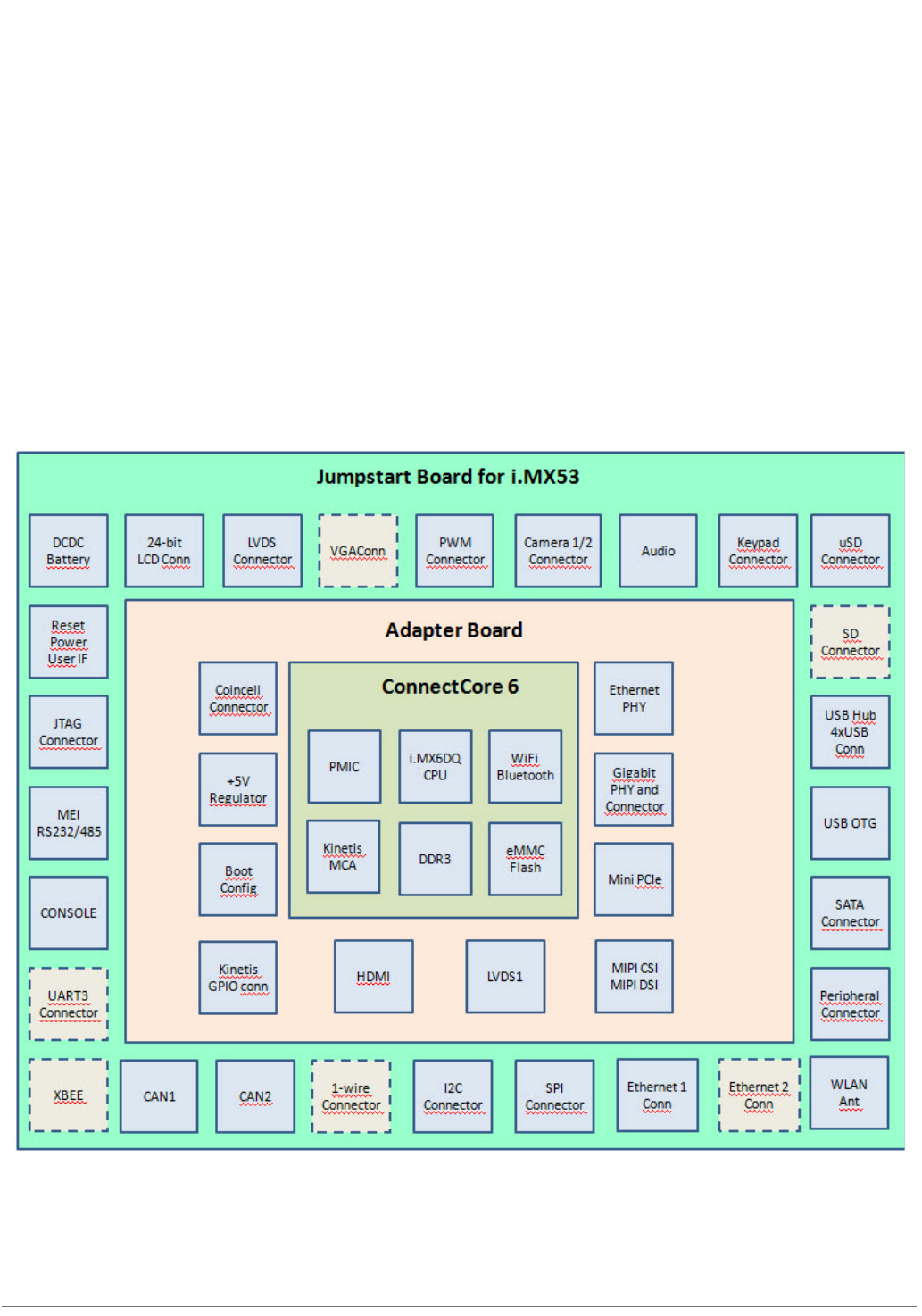
© 2014 Digi International Inc. 53
ConnectCore for i.MX6 Hardware Reference Manual
About the ConnectCore 6 Adapter Board
The ConnectCore 6 adapter board allows connecting the ConnectCore 6 module to the Jumpstart
board for the i.MX53 (JSCCWMX53), providing connections and hardware to use most of the
interfaces of the module for initial development and prototyping.
The ConnectCore 6 module is soldered on the adapter board. The adapter has two 2x90 pin
connectors for connecting the board to the JSCCWMX53.
The following picture shows the block diagram of hardware formed by the ConnectCore 6, the
adapter board and the JSCCWMX53. Dash boxes represent interfaces of the JSCCWMX53 that
are not connected to the adapter board.
Refer to the Single Board Computer (SBC) development board design information posted on the
Digi technical support website for a reference design based on a discrete implementation without
using an adapter board.
Hardware block diagram of the ConnectCore 6
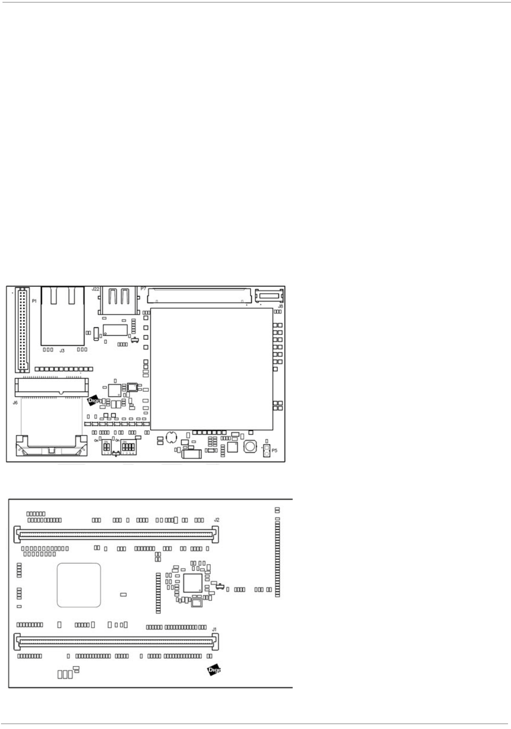
© 2014 Digi International Inc. 54
ConnectCore for i.MX6 Hardware Reference Manual
Features of the ConnectCore 6 Adapter Board
• ConnectCore 6 module
• Boot mode and boot source configuration switches
• +5V regulator
• Coin cell connector to supply the on module RTC
• Gigabit Ethernet PHY
• Gigabit Ethernet connector with link and speed LEDs
• HDMI connector
• LVDS1 connector
• MIPI Camera & MIPI Display connector
• PCI express mini card connector
• Connector for the Kinetis GPIO signals and SWD (single wire debug) interface.
• Two 2x90 pin connectors for connecting the board to the JSCCWMX53
ConnectCore 6 Adapter Board
Top side
Bottom side
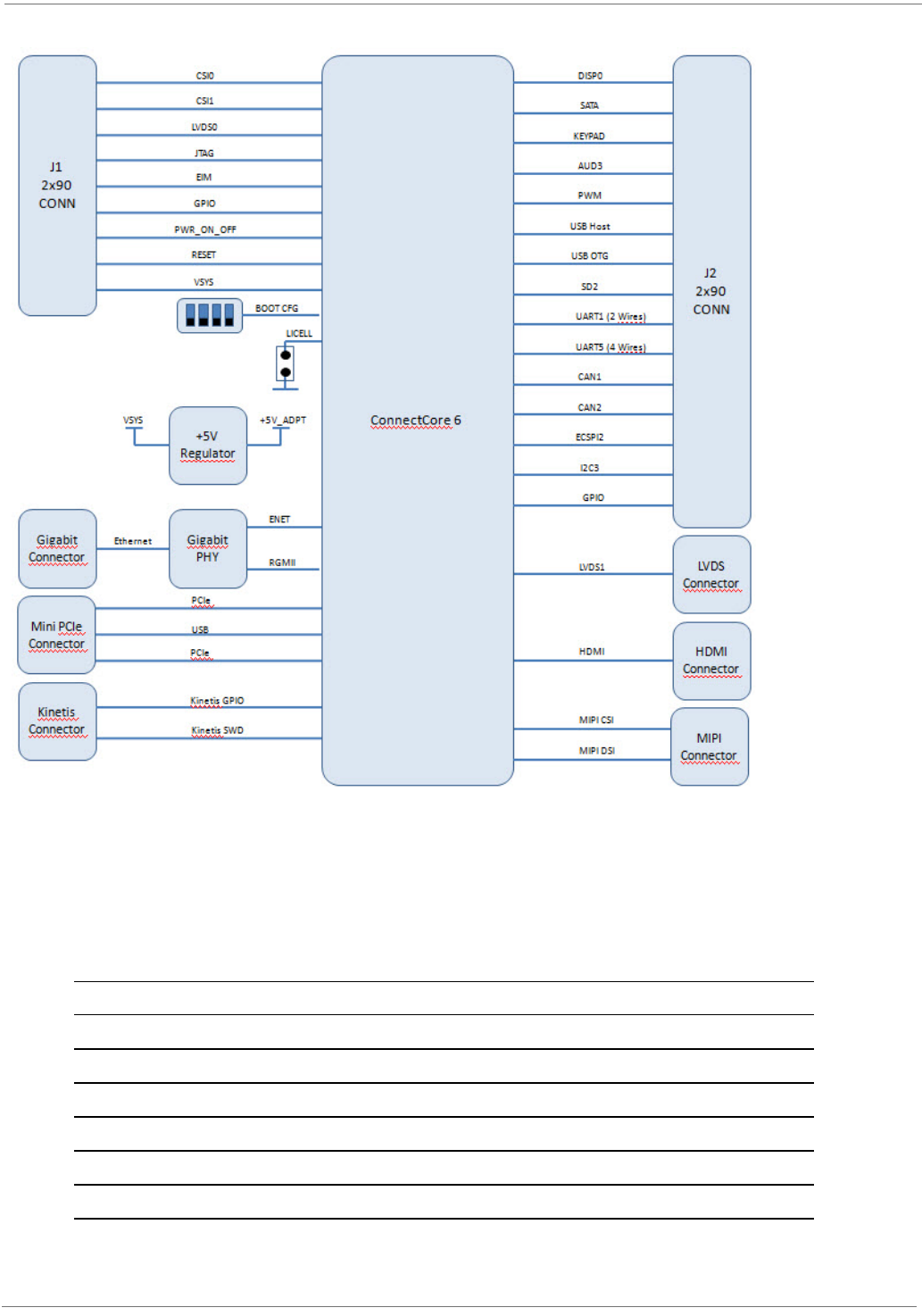
© 2014 Digi International Inc. 55
ConnectCore for i.MX6 Hardware Reference Manual
Block Diagram
ConnectCore 6 GPIO Assignments
The table below show the default GPIO assignments done on the ConnectCore 6 module on the
adapter board.
Signal name GPIO Use on the adapter board
NAND_D0 GPIO2_0 Audio Headphone detection
NAND_D1 GPIO2_1 JSCCWMX53 Touch IRQ
NAND_D2 GPIO2_2 User LED1
NAND_D3 GPIO2_3 User LED2
NAND_D4 GPIO2_4 User Key 1
NAND_D5 GPIO2_5 User Key 2

© 2014 Digi International Inc. 56
ConnectCore for i.MX6 Hardware Reference Manual
I2C Address Table
The ConnectCore 6 module has three I2C busses available on the module pinout. The default
configuration of the adapter board uses I2C2 and I2C3 busses. The following tables show the
configuration and use of these two I2C busses on the adapter board.
I2C2
This I2C bus is used internally on the ConnectCore 6 module. The bus is connected to the PMIC
and to the Kinetis MCA, and it's used to configure and monitor the PMIC.
This I2C bus is available on the module PADs, but should not be used unless absolutely
necessary. A problem on this bus can cause the module to not boot correctly.
Two 4K7 pull-up resistors to 3.3V are connected to the I2C2 lines on the ConnectCore 6 module.
The following table shows the interfaces connected to the I2C2 bus.
I2C3
The I2C bus is not used internally on the ConnectCore 6 module. Two 2K2 pull-up resistors to
3.3V are connected to the I2C3 lines on the adapter board.
NAND_D6 GPIO2_6 EIM IRQ
NAND_D7 GPIO2_7 JSCCWMX53 DIGIO0
EIM_CSI GPIO2_24 JSCCWMX53 DIGIO1
EIM_EB0 GPIO2_28 JSCCWMX53 DIGIO2
EIM_EB1 GPIO2_29 JSCCWMX53 DIGIO3
EIM_DA10 GPIO3_10 USB Hub reset
EIM_DA15 GPIO3_15 CSI1 Reset / Key Col 7
EIM_WAIT GPIO5_0 CSI0 Reset / Key Row 7
EIM_BCLK GPIO6_31 MIPI Backlight control
SD3_DAT2 GPIO7_6 MIPI GPIO
SD3_DAT3 GPIO7_7 PCIe Mini Card Wake up
SD3_RST GPIO7_8 PCIe Mini Card Reset
GPIO_16 GPIO7_11 LVDS1 Touch IRQ
Interface Speed (Kbps) Address
Kinetis MCA 400 SW configurable
PMIC 400 Write: 0xB0
Read: 0xB1
Module PADs 400
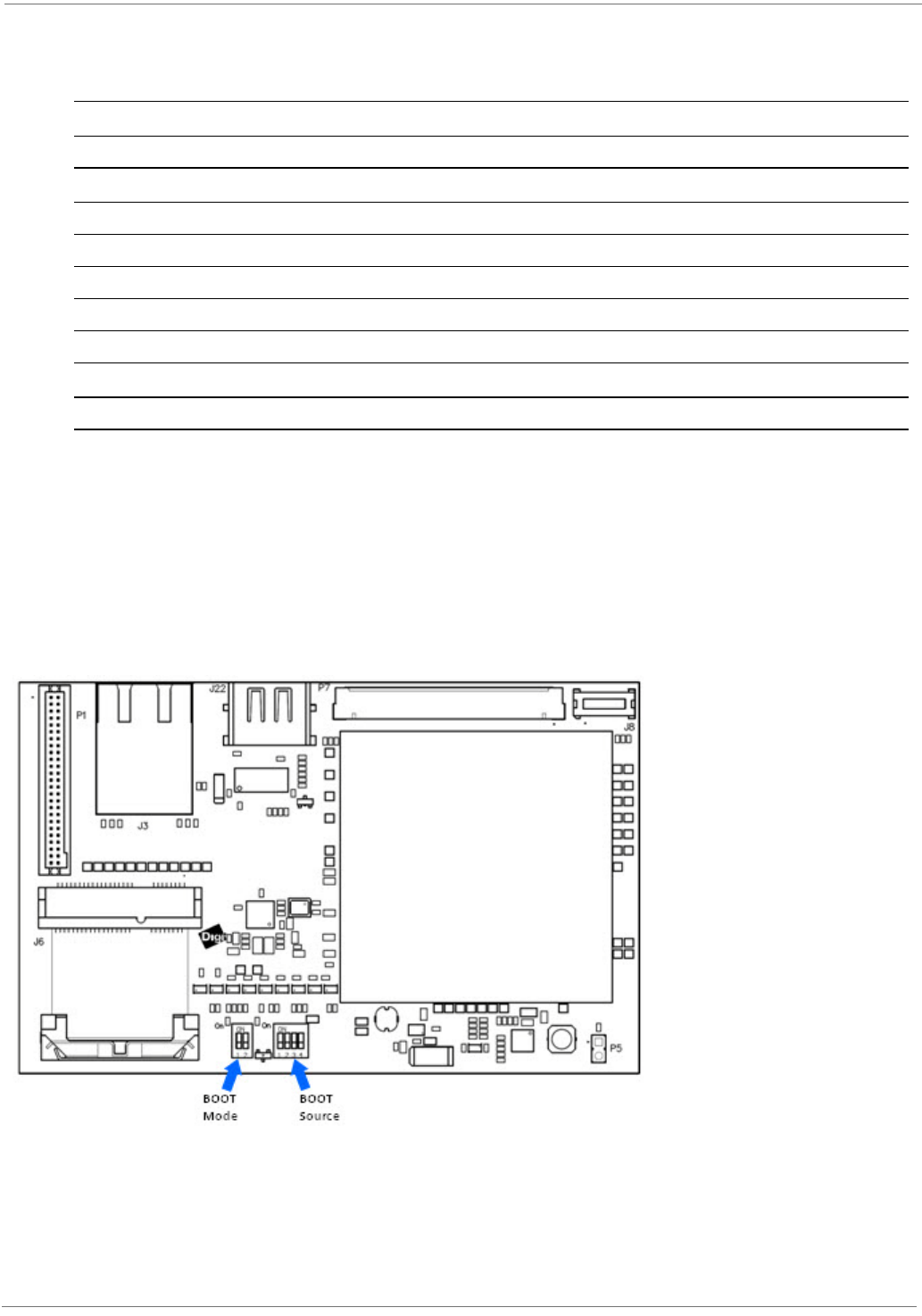
© 2014 Digi International Inc. 57
ConnectCore for i.MX6 Hardware Reference Manual
The following table shows the interfaces connected to the I2C3 bus.
(1) The JSCCWMX53 has an HDMI transmitter. This device is not used because an HDMI
transmitter is already integrated on the ConnectCore 6 module.
(2) The JSCCWMX53 has an EM3027 RTC device. This device is not used because an RTC
controller is already integrated on the ConnectCore 6 module.
Boot Switches for the ConnectCore 6
Boot Switches
Interface Speed (Kbps) Address Comment
HDMI EDID 100 0x50 Read only accesses
HDMI Transmitter 400 0x38, 0x39, 0x3F Not used (1)
MIPI Camera - - Depend on display used
PCIe mini card - - Depend on PCIe card used
Parallel LCD (touch) - - Depend on the LCD used
Audio CODEC 400 0x0A Address of SGTL5000
Peripheral Connector - - Depends on the device connected
RTC (2) 400 0x56 Address of EM3027 RTC
I2C connector - - Depends on the device connected
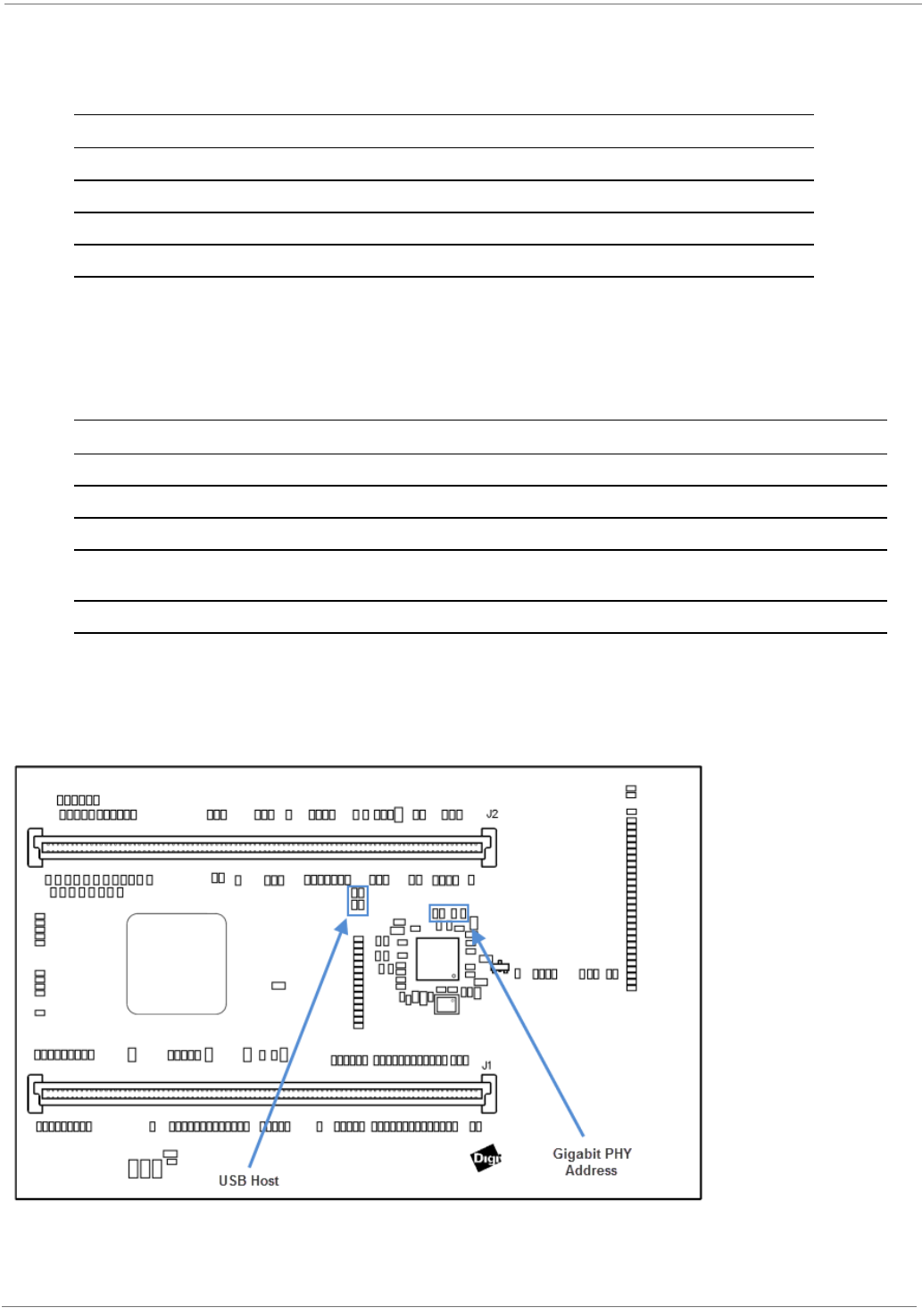
© 2014 Digi International Inc. 58
ConnectCore for i.MX6 Hardware Reference Manual
Boot Mode Switch, SW6
Use SW6 to configure the module boot mode:
Boot Source Switch, SW5
Use SW5 to configure the source of the boot code when SW6 is configured in boot from the
board settings mode.
Configuration Resistors for the ConnectCore 6
Configuration resistors
SW6 Pin 1 SW6 Pin 2 Comments
OFF OFF Boot from Fuses
ON OFF Serial downloader
OFF ON Boot from board settings
ON ON Reserved
SW5 Pin 1 SW5 Pin 2 SW5 Pin 3 SW5 Pin 3 Comments
ON ON OFF OFF Boot from eMMC, 1-bit data bus
OFF ON OFF OFF Boot from eMMC, 4-bit data bus
ON OFF OFF OFF Boot from eMMC, 8-bit data bus
ON - ON OFF Boot from microSD, 4-bit data
bus
- - OFF ON Boot from SATA
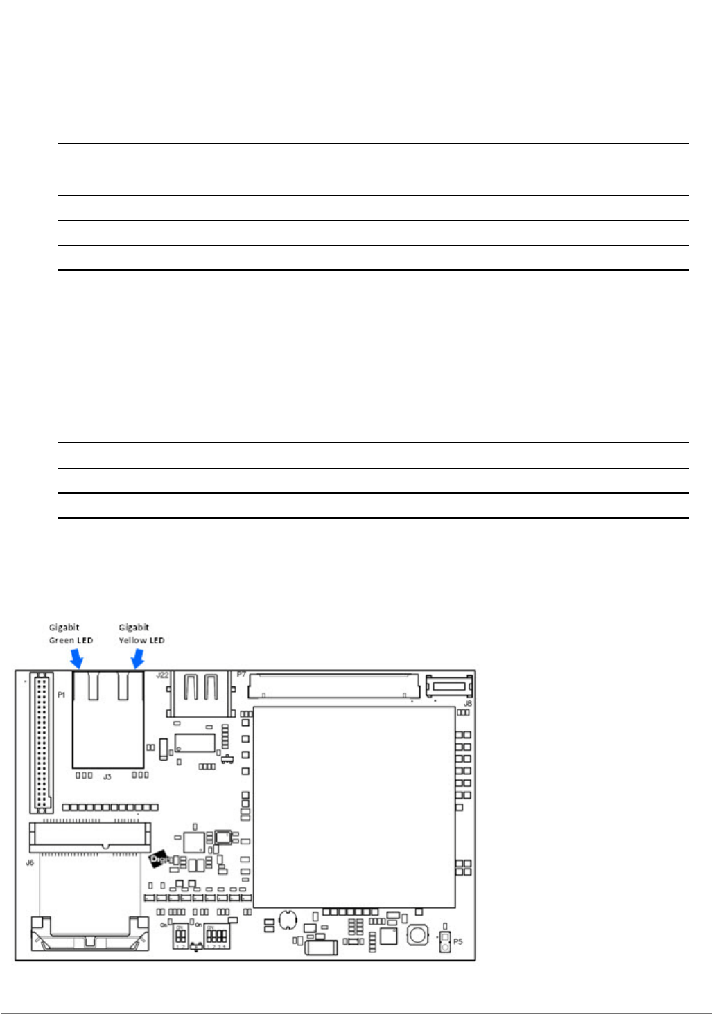
© 2014 Digi International Inc. 59
ConnectCore for i.MX6 Hardware Reference Manual
Gigabit Ethernet PHY Address
The adapter board has a Gigabit PHY for the Gigabit interface. The address of the Gigabit PHY
can be configured with four configuration resistors.
The Gigabit PHY address configured by default is 0x0.
USB Host
The ConnectCore 6 module provides one USB Host port. This USB port can be connected on the
adapter board to the PCIe mini card connector and to the JSCCWMX53. Four configuration
resistors are used to select the interface where the USB Host is connected.
By default the USB Host port is connected to the JSCCWMX53.
ConnectCore 6 Gigabit LEDs
Gigabit LEDs
R32 R24 R30 R31 PHY Address
NOT Populated Populated NOT Populated Populated 0x0
Populated NOT Populated NOT Populated Populated 0x1
NOT Populated Populated Populated NO Populated 0x2
Populated NOT Populated Populated NOT Populated 0x3
R678 R679 R658 R659 USB host connection
NOT Populated NOT Populated Populated Populated To JSCCWMX53
Populated Populated NOT Populated NOT Populated To PCIe
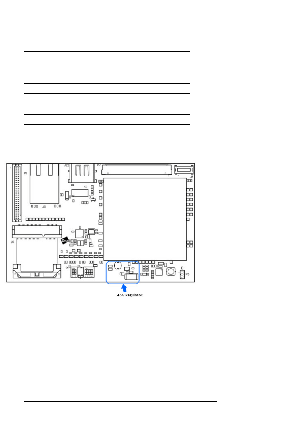
© 2014 Digi International Inc. 60
ConnectCore for i.MX6 Hardware Reference Manual
Gigabit Ethernet LEDs
The Gigabit Ethernet PHY has two outputs to indicate the link and activity status of the port.
These outputs are connected to a green LED and to a yellow LED, integrated on the Ethernet
connector. The following table shows the link/activity status indicated by the two LEDs.
5V Regulator
The adapter board has several interfaces that need a regulated 5V supply. To generate this
supply one LTC3125 step-up DC/DC converter is used. This DC/DC converted can generate a
regulated 5V from a 1.8V to 5.5V input supply. The LTC3125 will maintain voltage regulation
even when the input voltage is above the desired output voltage.
The 5V regulator will be enabled by the ConnectCore 6 signal PWR_EN. On low power mode this
regulator will be disabled. The following table shows the interfaces of the adapter board where
the +5V supply is connected.
Yellow LED Green LED Link/Activity Status
OFF OFF Link off
ON OFF 1000 Link/ No activity
Blinking OFF 1000 Link/ activity (Rx, Tx)
OFF ON 100 Link/ No activity
OFF Blinking 100 Link/Activity (Rx, Tx)
ON ON 10 Link/ No activity
Blinking Blinking 10 Link/ activity (Rx, Tx)
Interface Comments
USBH1_VBUS Power supply for the USB Host controller of the i.MX6 CPU
LVDS1 Supply for the LVDS backlight
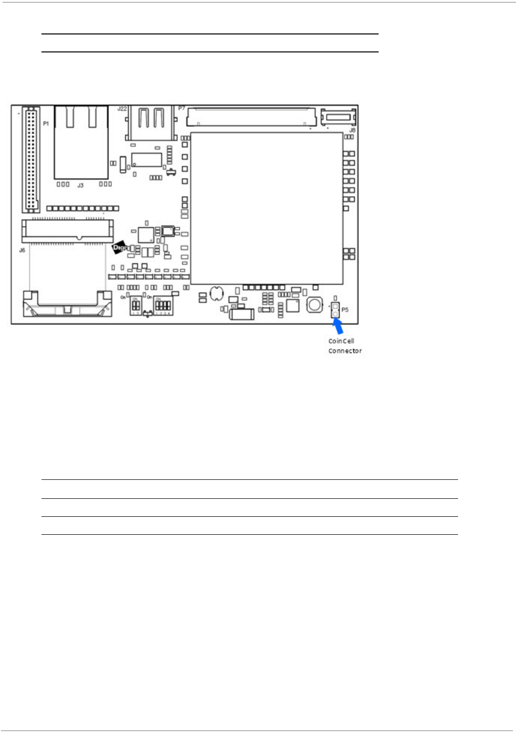
© 2014 Digi International Inc. 61
ConnectCore for i.MX6 Hardware Reference Manual
Coin Cell Connector
Coin Cell Connector, P5
The adapter board provides a 2-pin, 2.54mm pitch straight pin header for connecting an external
coin cell or super capacitor to power the RTC interface when the main supply is off. If higher
voltage is present on the main supply, it will be used as a power source for the RTC.
The following table shows the pinout of the coin cell connector.
There are three types of components that can be connected to this connector: Lithium coin cells
(Primary cell: non-rechargeable), Lithium coin cells (Secondary cell: rechargeable), and
Supercaps. When a Primary Lithium coin cell is connected, the PMIC backup battery charger
must be turned off and this pin is used strictly as an input. It is hazardous to attempt to charge
Primary Lithium cells as they may vent or explode. Secondary Lithium coin cells are only made
available directly to manufacturers of equipment that could use them, in that case they are
normally required to design their product to prevent the user gaining access to this part since
there is a danger to the user if by replacing it, they fit a primary type (the only sort that they are
likely to be able to source) into the charging circuit. When a Secondary Lithium coin cell is used,
both the charging current and the termination voltage are programmable. When a Supercap is
used, both the charge current and termination voltage should be set to the maximum values.
HDMI Supply for HDMI display
MIPI Supply for MIPI camera and display
Pin Signal Comments
1 VCC_LICELL Power supply for RTC
2 GND Ground
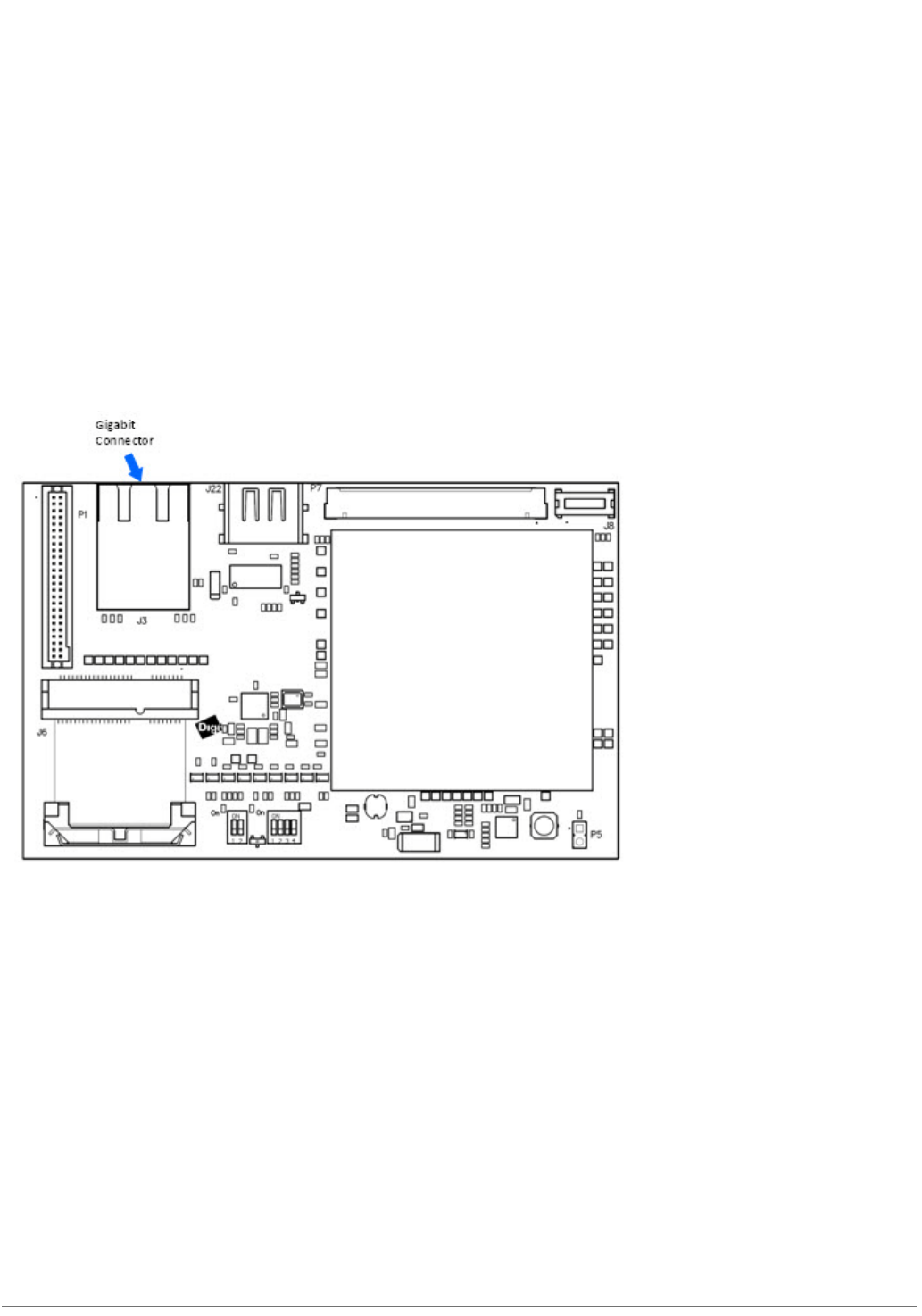
© 2014 Digi International Inc. 62
ConnectCore for i.MX6 Hardware Reference Manual
The advantage of using a Primary Lithium coin cell is that the energy density usually allows years
of service since the self discharge rate is low. The advantage of using a Secondary Lithium coin
cell is that the self discharge rate is usually sufficient to allow a few months of support for the
RTC before it will need recharging. The advantage of the Supercap is that it is intrinsically safe
and can out-last the Primary Lithium coin cell option, however the self discharge rate is high
meaning that a 1F capacitor at 25° C is likely to support the RTC for approximately 5 to 10 days.
A programmable constant charge current charger with a programmable top-off charging voltage
is provided for charging of Secondary Lithium-Manganese coin cell batteries and super
capacitors. Charging current is programmable from 100uA to 6mA. Termination voltage is
programmable from +1.1 to +3.1V.
The minimum voltage of the coin cell supply is +2V. The maximum voltage of the coin cell supply
is +3.6V.
Gigabit Ethernet
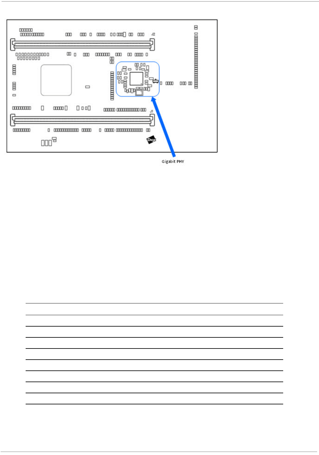
© 2014 Digi International Inc. 63
ConnectCore for i.MX6 Hardware Reference Manual
Gigabit PHY
The adapter board has a triple-speed (10Base-T/100Base-Tx/1000Base-T) Ethernet PHY
connected to the RGMII interface of the ConnectCore 6 module. Two GPIO signals of the i.MX6
CPU are used to reset the Ethernet PHY (GPIO1_25) and as interrupt input from the PHY
(GPIO1_28).
Gigabit Connector, J3
The adapter board provides a Gigabit RJ-45 connector with integrated 1:1 transformer and link/
activity LEDs. The functionality of the two LEDs is detailed on chapter Gigabit Ethernet LEDs.
The following table shows the pinout of the Gigabit connector.
Pin Signal Comments
1 TRP1+ Transmit and receive pair 1 data +
2 TRP1- Transmit and receive pair 1 data -
3 TRP2+ Transmit and receive pair 2 data +
4 TRP2- Transmit and receive pair 2 data -
5 TRP3+ Transmit and receive pair 3 data +
6 TRP3- Transmit and receive pair 3 data -
7 TRP4+ Transmit and receive pair 4 data +
8 TRP4- Transmit and receive pair 4 data -
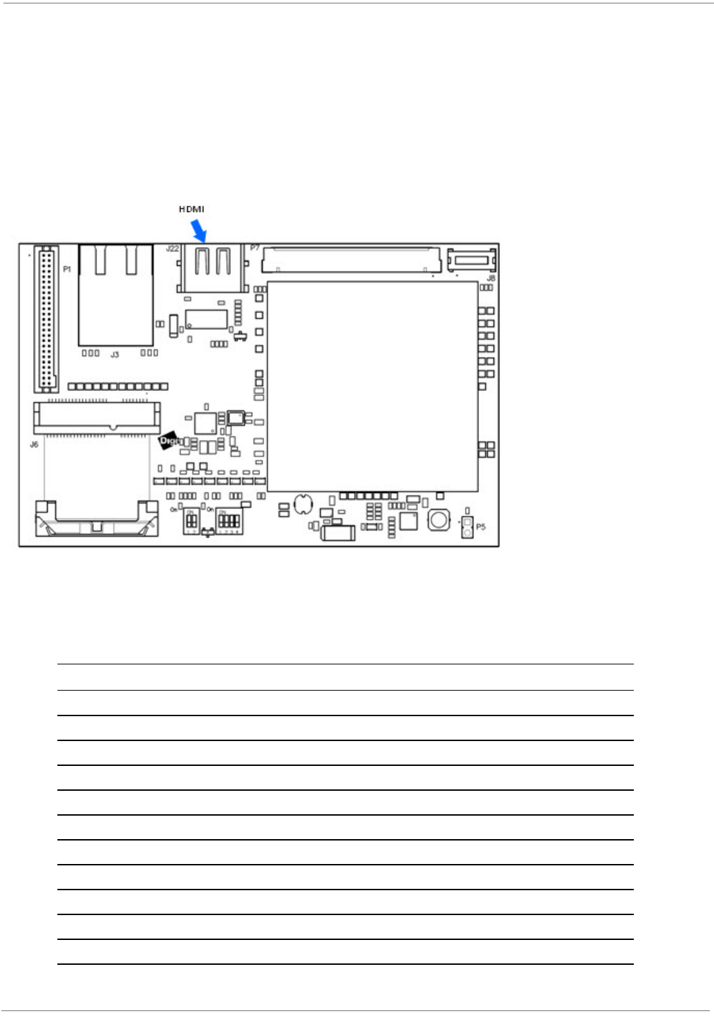
© 2014 Digi International Inc. 64
ConnectCore for i.MX6 Hardware Reference Manual
HDMI
The ConnectCore 6 module provides an HDMI 1.4a compatible interface. The interface includes
the HDMI controller and PHY. Video resolutions up to 1080p@120Hz HDTV are supported. All
audio formats as specified by the HDMI Specification 1.4a are supported. Hot plug/unplug
detection is also supported.
The adapter board provides an HDMI port protection device with all ESD, overcurrent output
protection and backdrive protection for an HDMI port.
HDMI Connector, J22
The adapter board provides an HDMI connector, J22. The table below shows the pinout of the
HDMI connector.
Pin Signal Comments
1 HDMI_TX2+ Transmit and receive pair 2 data +
2 GND Data2 shield
3 HDMI_TX2- Transmission pair2 data-
4 HDMI_TX1+ Transmission pair1 data+
5 GND Data 1 shield
6 HDMI_TX1- Transmission pair 1 data-
7 HDMI_TX0+ Transmission pair 0 data+
8 GND Data0 shield
9 HDMI_TX0- Transmission pair 0 data-
10 HDMI_TXC+ Transmission pair clock+
11 GND Clock shield
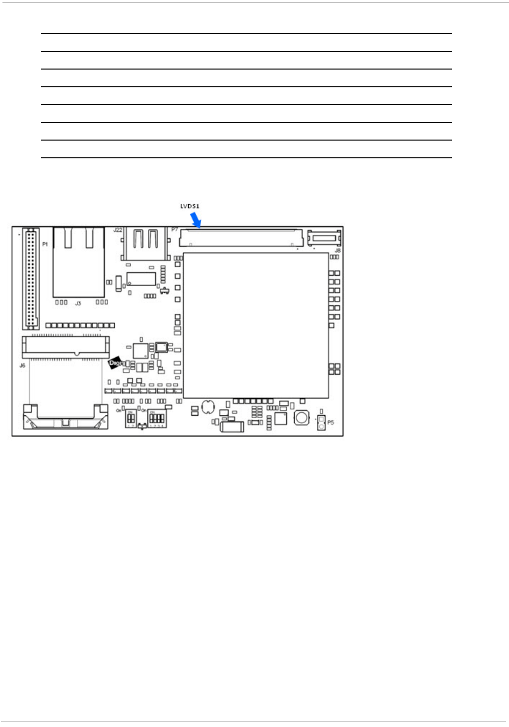
© 2014 Digi International Inc. 65
ConnectCore for i.MX6 Hardware Reference Manual
LVDS1
LVDS Interface
The adapter board provides a 30 pin, 1.25mm pitch connector (Hirose DF14-30P-1.25H) for
accessing the ConnectCore 6 LVDS1 interface.
The LVDS connector provides access to the following LVDS capabilities:
• 4 LVDS differential data pairs
• 1 LVDS differential clock pair
• SPI bus for an external touch screen controller
• Interrupt input for touch screen
• PWM output to control the backlight brightness
• +3.3VDC and +5VDC supplies
12 HDMI_TXC- Transmission pair clock-
13 NC Consumer electronic control
14 NC Reserved
15 HDMI_SCL I2C SCL
16 HDMI_SDA I2C SDA
17 GND DDC/CEC Ground
18 +5V 5V supply (50mA max)
19 HOTPLUG_DET Hot plug detection

© 2014 Digi International Inc. 66
ConnectCore for i.MX6 Hardware Reference Manual
LVDS Connector, P7
The table below shows the pinout of the LVDS1 connector, P7:
MIPI Camera and MIPI Display
The ConnectCore 6 board provides a MIPI camera serial interface (MIPI_CSI) compliant with the
MIPI CSI-2 specification. A MIPI D-PHY is also included on the module, allowing direct
connections between the module and a MIPI CSI-2 compliant camera sensor. This interface
supports up to 4 differential data pairs.
Pin Signal Comments
1 +3.3V Generated on PMIC buckperi
2 +3.3V Generated on PMIC buckperi
3 GND
4 LVDS1_TX0_N Transmission pair 0 data -
5 LVDS1_TX0_P Transmission pair 0 data +
6 GND
7 LVDS1_TX1_N Transmission pair 1 data-
8 LVDS1_TX1_P Transmission pair 1 data +
9 GND
10 LVDS1_TX2_N Transmission pair 2 data-
11 LVDS1_TX2_P Transmission pair 2 data+
12 GND
13 LVDS1_CLK_N Transmission pair clock-
14 LVDS1_CLK_P Transmission pair clock+
15 GND
16 LVDS1_TX3_N Transmission pair 3 data-
17 LVDS1_TX3_P Transmission pair 3 data+
18 GND
19 nc
20 nc
21 nc
22 nc
23 LVDS1_PENIRQ# Connected to i.MX6 GPIO_16 pad
24 ECSPI2_MOSI
25 ECSPI2_MISO
26 ECSPI2_CLK
27 ECSPI2_SS1 Connected to i.MX6 EIM_LBA pad
28 PWM1 Shared with MIPI display
29 +5V Generated on adapter board
30 +5V Generated on adapter board
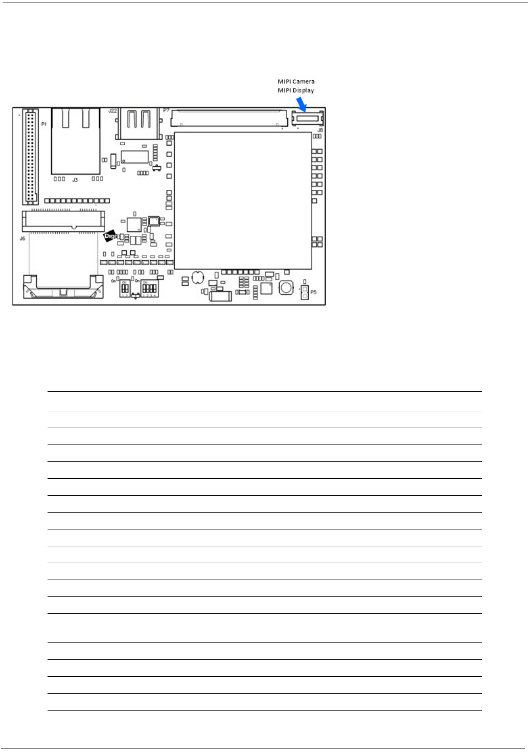
© 2014 Digi International Inc. 67
ConnectCore for i.MX6 Hardware Reference Manual
The ConnectCore for iMX6 board provides a MIPI display serial interface (MIPI_DSI) compliant
with the MIPI DSI specification. A MIPI D-PHY is also included on the module, allowing direct
connections between the module and a MIPI DSI compliant display. This interface supports up to
2 differential data pairs.
MIPI Connector
The adapter board provides a 2x15 pin, 0.5mm pitch connector (Molex 54167-0308) for the MIPI
interfaces. The following table shows the pinout of the MIPI connector.
Pin Signal Comments
1 +5V Supply for camera and display
2 CSI_D0_N MIPI Camera pair 0 data-
3 +5V Supply for camera and display
4 CSI_D0_P MIPI Camera pair 0 data+
5 MIPI_I2C_SDA I2C2 bus
6 GND
7 MIPI_I2C_SCL I2C2 bus
8 CSI_D1_N MIPI Camera pair 1 data-
9 PWM1 Shared with LVDS1 interface
10 CSI_D1_P MIPI Camera pair 1 data+
11 MIPI_BACKLGT_ON MIPI Display Backlight control
12 GND
13 MIPI_GPIO Can be used to reset or disable a MIPI Camera or
display
14 CSI_D2_N MIPI Camera pair 2 data-
15 DSI_D0_P MIPI Display pair 0 data+
16 CSI_D2_P MIPI Camera pair 2 data+
17 DSI_D0_N MIPI Display pair 0 data-

© 2014 Digi International Inc. 68
ConnectCore for i.MX6 Hardware Reference Manual
PCI Express Mini Card Interface
The ConnectCore 6 module provides a PCI express controller and a PCI express PHY. The
adapter board has a half size mini PCIe card connector (J6) to support this interface.
The following interfaces are connected to the PCIe card connector:
• PCIe: Three differential pairs for transmit data, receive data and clock
• I2C3
• USB Host 2.0. This interface is shared with the USB connected to the JSCCWMX53. Please
refer to chapter Configuration Resistors to connect this interface for the PCIe connector
• PCIE_WAKE_N: output, open drain, low level signal to wake up the module
• PCIE_RESET_N: low level signal to reset the mini PCIe card.
18 GND
19 GND
20 CSI_D3_N MIPI Camera pair 3 data-
21 DSI_CLK0_P MIPI Display clock+
22 CSI_D3_P MIPI Camera pair 3 data
23 DSI_CLK0_N MIPI Display clock-
24 GND
25 GND
26 CSI_CLK0_N MIPI Camera clock-
27 DSI_D1_P MIPI Display pair 1 data+
28 CSI_CLK0_P MIPI Camera clock+
29 DSI_D1_N MIPI Display pair 1 data-
30 GND

© 2014 Digi International Inc. 69
ConnectCore for i.MX6 Hardware Reference Manual
PCI Express Mini Card Connector
The following table shows the pinout of the PCI express mini card connector.
Pin Signal Comments
1PCIE_WAKE_N
23.3V
3-
4 GND
5-
61.5V
7-
8-
9 GND
10 -
11 PCIE_CLK_N
12 -
13 PCIE_CLK_P
14 -
15 GND
16 -
17 -
18 GND
19 -
20 -
21 GND
22 PCIE_RESET_N
23 PCIE_RX_N
24 +3.3V
25 PCIE_RX_P
26 GND
27 GND
28 +1.5V
29 GND
30 I2C3_SCL
31 PCIE_TX_N
32 I2C3_SDA
33 PCIE_TX_P
34 GND
35 GND
36 USB_DN
37 GND

© 2014 Digi International Inc. 70
ConnectCore for i.MX6 Hardware Reference Manual
Kinetis Microcontroller Assistant, MCA
The ConnectCore 6 module has a Kinetic microcontroller for wake up, power management
control, and analogue and digital GPIO expander.
The MCA can be programmed through the Serial Wire Debug (SWD) interface. These signals are
available on the module pinout and are connected on the adapter board to the MCA connector.
All the MCA signals that are not used internally on the ConnectCore 6 module are connected to
the module pinout. These signals can be used as GPIO, low leakage wake up sources, PWM
outputs, etc. On the adapter these signals are connected to the MCA connector.
Kinetis MCA Connector, P1
The adapter provides a 2x25 pin, 1.27mm pitch, pin header (SAMTEC TFM-125-32-L-D-A) for the
Kinetis MCA signals. Four of these signals are connected to the ConnectCore 6 module and also
to the touch screen inputs of the JSCCWMX53. The following table shows the pinout of this
connector.
38 USB_DP
39 +3.3V
40 GND
41 +3.3V
42 -
43 GND
44 -
45 -
46 -
47 -
48 +1.5V
49 -
50 GND
51 -
52 +3.3V
Pin Signal Comments
1 VLDO3_MCA +3.3V supply
2 MCA_SWD_DIO Single wire debug (SWD) data
3 GND
4 MCA_SWD_CLK Single wire debug (SWD) clock
5 GND
6-
7-
8-

© 2014 Digi International Inc. 71
ConnectCore for i.MX6 Hardware Reference Manual
9-
10 MCA_RESET_N Input signal to reset the MCA
11 GND
12 GND
13 MCA_PTA1
14 MCA_PTA4
15 MCA_PTA19
16 -
17 GND
18 GND
19 MCA_PTB0 Also connected to Touch input from the JSCCWMX53
20 MCA_PTB1
21 MCA_PTB16
22 MCA_PTB17
23 GND
24 GND
25 MCA_PTC0 Also connected to Touch input from the JSCCWMX53
26 MCA_PTC2 Also connected to Touch input from the JSCCWMX53
27 MCA_PTC3
28 MCA_PTC4
29 MCA_PTC5
30 MCA_PTC6
31 MCA_PTC7
32 -
33 GND
34 GND
35 MCA_PTD4
36 MCA_PTD5
37 MCA_PTD6
38 MCA_PTD7
39 GND
40 GND
41 MCA_IO/USB0_P
42 MCA_IO/USB0_N
43 MCA_PTE18
44 MCA_PTE19
45 MCA_PTE20 Also connected to Touch input from the JSCCWMX53
46 MCA_PTE21
47 MCA_PTE25
48 MCA_PTE29
49 GND
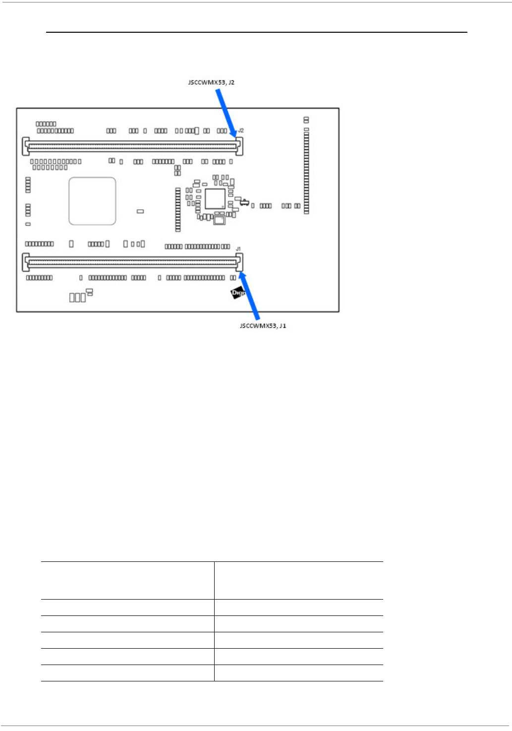
© 2014 Digi International Inc. 72
ConnectCore for i.MX6 Hardware Reference Manual
Connectors for JSCCWMX53
The adapter board has two 2x90 pin connectors, J1 and J2, for connecting the board to the
Jumpstart Kit for CCW-i.MX53 board.
Most of the interfaces of the ConnectCore 6 are directly connected to the JSCCWMX53. Please
refer to chapter Block Diagram to see the interfaces that are directly connected between the
ConnectCore 6 and the JSCCWMX53 board.
The following paragraphs detail the connections between the ConnectCore 6 module and the
JSCCWMX53. For a detailed description of the JSCCWMX53 board please refer to the Hardware
Reference Manual of the JSCCWMX53.
Parallel Camera 0, CSI0
The following table shows the signals mapping between the parallel camera 0 of the adapter
board and the parallel camera 0 of the JSCCWMX53.
50 GND
JSCCWMX53 Adapter board
Signal name Pin Signal name Pin
CSI0_D12 J1-5 CSI0_D12 L5
CSI0_D13 J1-6 CSI0_D13 C6
CSI0_D14 J1-7 CSI0_D14 B6
CSI0_D15 J1-8 CSI0_D15 E6
CSI0_D16 J1-9 CSI0_D16 H6
© 2014 Digi International Inc. 73
ConnectCore for i.MX6 Hardware Reference Manual
Parallel Camera 1, CSI1
The following table shows the signals mapping between the parallel camera 1 of the adapter
board and the parallel camera 1 of the JSCCWMX53.
LVDS0
The following table shows the signals mapping between the LVDS0 interface of the adapter
board and the LVDS0 interface of the JSCCWMX53.
CSI0_D17 J1-10 CSI0_D17 A7
CSI0_D18 J1-11 CSI0_D18 F6
CSI0_D19 J1-12 CSI0_D19 G6
CSI0_VSYNC J1-13 CSI0_VSYNC J5
CSI0_HSYNC J1-14 CSI0_MCLK A5
CSI0_PIXCLK J1-15 CSI0_PIXCLK G5
CSI_MCLK J1-16 GPIO_0 G2
CSI0_RESET_N J1-2 MX6_EIM_WAIT AA13
JSCCWMX53 Adapter board
Signal name Pin Signal name Pin
CSI1_D12 J1-160 EIM_A17 AC17
CSI1_D13 J1-163 EIM_A18 AB15
CSI1_D14 J1-162 EIM_A19 AD16
CSI1_D15 J1-165 EIM_A20 AB16
CSI1_D16 J1-164 EIM_A21 AC16
CSI1_D17 J1-167 EIM_A22 AC19
CSI1_D18 J1-166 EIM_A23 AA14
CSI1_D19 J1-169 EIM_A24 AD17
CSI1_VSYNC J1-137 EIM_DA12 V22
CSI1_HSYNC J1-134 EIM_DA11 V18
CSI1_PIXCLK J1-161 EIM_A16 AD15
CSI_MCLK J1-16 GPIO_0 G2
CSI1_RESET_N J1-1 EIM_DA15 Y20
JSCCWMX53 Adapter board
Signal name Pin Signal name Pin
LVDS0_CLK_N J1-63 LVDS0_CLK_N M4
LVDS0_CLK_P J1-65 LVDS0_CLK_P L4
LVDS0_TXD0_N J1-67 LVDS0_TXD0_N J4
LVDS0_TXD0_P J1-69 LVDS0_TXD0_P H4
LVDS0_TXD1_N J1-71 LVDS0_TXD1_N F4
© 2014 Digi International Inc. 74
ConnectCore for i.MX6 Hardware Reference Manual
JTAG
The following table shows the signals mapping between the JTAG interface of the adapter board
and the JTAG interface of the JSCCWMX53.
LVDS0_TXD1_P J1-73 LVDS0_TXD1_P E4
LVDS0_TXD2_N J1-75 LVDS0_TXD2_N C4
LVDS0_TXD2_P J1-77 LVDS0_TXD2_P B4
LVDS0_TXD3_N J1-79 LVDS0_TXD3_N R4
LVDS0_TXD3_P J1-81 LVDS0_TXD3_P P4
JSCCWMX53 Adapter board
Signal name Pin Signal name Pin
JTAG_TCK J1-91 JTAG_TCK F13
JTAG_TRST_N J1-92 JTAG_TRST_N D15
JTAG_TMS J1-93 JTAG_TMS F14
JTAG_MOD J1-94 JTAG_MOD G13
JTAG_TDI J1-95 JTAG_TDI D15
JTAG_TDO J1-97 JTAG_TDO E14

© 2014 Digi International Inc. 75
ConnectCore for i.MX6 Hardware Reference Manual
EIM
The ConnectCore 6 module provides an external interface module (EIM) to connect memory
mapped devices. This module is highly configurable to different modes, data length, address
length, etc. Most of the pins of the EIM are multiplexed with other functionalities. The following
table shows the signal mapping of the EIM signals between the JSCCWMX53 and the adapter
board module.
JSCCWMX53 Adapter board
Signal name Pin Signal name Pin
EIM_DA0 J1-121 EIM_DA0 U20
EIM_DA1 J1-122 EIM_DA1 W23
EIM_DA2 J1-123 EIM_DA2 V24
EIM_DA3 J1-124 EIM_DA3 U19
EIM_DA4 J1-127 EIM_DA4 W24
EIM_DA5 J1-126 EIM_DA5 AA19
EIM_DA6 J1-129 EIM_DA6 U23
EIM_DA7 J1-128 EIM_DA7 Y21
EIM_DA8 J1-131 EIM_DA8 W22
EIM_DA9 J1-132 EIM_DA9 V19
EIM_D16 J1-141 EIM_D16 AD20
EIM_D17 J1-142 EIM_D17 V17
EIM_D18 J1-143 EIM_D18 AB18
EIM_D19 J1-144 EIM_D19 Y17
EIM_D20 J1-147 EIM_D20 W19
EIM_D21 J1-146 EIM_D21 Y16
EIM_D22 J1-149 EIM_D22 Y18
EIM_D23 J1-148 EIM_D23 AC20
EIM_D24 J1-151 EIM_D24 W20
EIM_D25 J1-152 EIM_D25 AA17
EIM_D26 J1-153 EIM_D26 AD19
EIM_D27 J1-154 EIM_D27 AD18
EIM_D28 J1-157 EIM_D28 AB17
EIM_D29 J1-156 EIM_D29 W16
EIM_D30 J1-159 EIM_D30 Y115
EIM_D31 J1-158 EIM_D31 AA15
EIM_OE J1-172 EIM_OE V15
EIM_RW J1-174 EIM_RW W15
EIM_CS0 J1-113 EIM_CS0 AB13
EIM_EB2 J1-177 EIM_EB2 Y24
EIM_EB3 J1-179 EIM_EB3 AA18
EIM_IRQ J1-178 NANDF_D6 G22

© 2014 Digi International Inc. 76
ConnectCore for i.MX6 Hardware Reference Manual
Display 0
The following table shows the signals mapping between the display 0 interface of the adapter
board and the Display 0 interface of the JSCCWMX53.
SATA
The following table shows the signals mapping between the SATA interface of the adapter board
and the SATA interface of the JSCCWMX53.
JSCCWMX53 Adapter board
Signal name Pin Signal name Pin
DISP0_DAT0 J2-1 DISP0_DAT0 AC8
DISP0_DAT1 J2-2 DISP0_DAT1 AC9
DISP0_DAT2 J2-3 DISP0_DAT2 AD9
DISP0_DAT3 J2-4 DISP0_DAT3 AB8
DISP0_DAT4 J2-5 DISP0_DAT4 AA9
DISP0_DAT5 J2-6 DISP0_DAT5 AD7
DISP0_DAT6 J2-7 DISP0_DAT6 AB7
DISP0_DAT7 J2-8 DISP0_DAT7 AC7
DISP0_DAT8 J2-9 DISP0_DAT8 AA8
DISP0_DAT9 J2-10 DISP0_DAT9 AB6
DISP0_DAT10 J2-11 DISP0_DAT10 Y8
DISP0_DAT11 J2-12 DISP0_DAT11 Y7
DISP0_DAT12 J2-13 DISP0_DAT12 AA7
DISP0_DAT13 J2-14 DISP0_DAT13 W8
DISP0_DAT14 J2-15 DISP0_DAT14 AC6
DISP0_DAT15 J2-16 DISP0_DAT15 W7
DISP0_DAT16 J2-17 DISP0_DAT16 V6
DISP0_DAT17 J2-18 DISP0_DAT17 AB5
DISP0_DAT18 J2-19 DISP0_DAT18 AD6
DISP0_DAT19 J2-20 DISP0_DAT19 Y6
DISP0_DAT20 J2-21 DISP0_DAT20 W6
DISP0_DAT21 J2-22 DISP0_DAT21 U6
DISP0_DAT22 J2-23 DISP0_DAT22 V7
DISP0_DAT23 J2-24 DISP0_DAT23 AA6
DISP0_HSYNC J2-25 DI0_PIN2 W10
DISP0_VSYNC J2-30 DI0_PIN3 V8
DISP0_CLK J2-28 DI0_DISP_CLK V9
DISP0_BIAS J2-31 DI0_PIN15 V10
PWM1 J2-27 DI0_PIN4 AD8
© 2014 Digi International Inc. 77
ConnectCore for i.MX6 Hardware Reference Manual
Touch
The JSCCWMX53 has four analog signals for a resistive touch screen connection. These four
analog inputs are connected to four analog input of the ConnectCore 6 module. These signals
are also connected to the Kinetis MCA connector on the adapter board.
The following table shows the signals mapping between the touch interface of the adapter board
and the touch interface of the JSCCWMX53.
Keypad
The following table shows the signals mapping between the keypad interface of the adapter
board and the keypad interface of the JSCCWMX53.
JSCCWMX53 Adapter board
Signal name Pin Signal name Pin
SATA_TX_N J2-33 SATA_TX_N D19
SATA_TX_P J2-35 SATA_TX_P E19
SATA_RX_N J2-34 SATA_RX_N G19
SATA_RX_P J2-36 SATA_RX_P H19
JSCCWMX53 Adapter board
Signal name Pin Signal name Pin
TOUCH_X1 J2-39 MCA_IO0 T23
TOUCH_X2 J2-41 MCA_IO2 R23
TOUCH_Y1 J2-43 MCA_IO4 U24
TOUCH_Y2 J2-45 MCA_IO9 R22
JSCCWMX53 Adapter board
Signal name Pin Signal name Pin
KEY_ROW2 J2-93 KEY_ROW0 E2
KEY_ROW3 J2-95 KEY_ROW2 H2
KEY_ROW5 J2-97 GPIO_2 G3
KEY_ROW7 J1-2 GPIO_5 R3
KEY_COL2 J2-90 KEY_COL0 J2
KEY_COL3 J2-92 KEY_COL2 K2
KEY_COL6 J2-94 GPIO_9 H3
KEY_COL7 J1-1 GPIO_4 L3

© 2014 Digi International Inc. 78
ConnectCore for i.MX6 Hardware Reference Manual
Audio
The following table shows the signals mapping between the audio interface of the adapter board
and the audio interface of the JSCCWMX53.
PWM
The ConnectCore 6 module has three PWM signals generated by the PMIC. Two of these PWM
signals are connected to the PWM signals of the JSCCWMX53. The other PWM signal is
connected to the LVDS1 connector and to the MIPI connector of the adapter board, to control
the intensity of these displays.
The following table shows the connection between the PWM signals of the adapter board and the
PWM signals of the JSCCWMX53.
The following table shows the connection between the PWM signal of the adapter board and the
LVDS1 connector of the adapter board.
The following table shows the connection between the PWM of the adapter board and the MIPI
connector of the adapter board.
JSCCWMX53 Adapter board
Signal name Pin Signal name Pin
AUD5_TXD J2-137 CSI0_DAT5 C7
AUD5_RXD J2-139 CSI0_DAT7 M5
AUD5_TXC J2-141 CSI0_DAT4 B7
AUD5_TXFS J2-144 CSI0_DAT6 C5
AUD_HP_DET J2-79 NANDF_D0 J24
JSCCWMX53 Adapter board
Signal name Pin Signal name Pin
PMIC_GPIO14/PWM1 J2-27 PMIC_GPIO14/PWM2 Y10
PMIC_GPIO15/PWM2 J2-32 PMIC_GPIO15/PWM3 V13
JSCCWMX53 Adapter board
Signal name Pin Signal name Pin
PMIC_GPIO11/PWM1 P4-28 PMIC_GPIO11/PWM1 V11
JSCCWMX53 Adapter board
Signal name Pin Signal name Pin
PMIC_GPIO11/PWM1 J6-9 PMIC_GPIO11/PWM1 V11

© 2014 Digi International Inc. 79
ConnectCore for i.MX6 Hardware Reference Manual
USB Host
The JSCCWMX53 has a USB Hub connected to the USB Host interface. The following table shows
the signals mapping between the USB Host interface of the adapter board and the USB Host
interface of the JSCCWMX53.
USB OTG
The JSCCWMX53 has a USB OTG interface with a reduced number of signals. The over current
(USB_OTG_OC) and power enable (USB_OTG_PWR) signals are not used.
The following table shows the signals used in the JSCCWMX53 for the USB OTG interface and the
mapping of these signals on the module.
SD2
The following table shows the signal mapping between the SD2 interface of the adapter board
and the SD3 interface of the JSCCWMX53.
Note: The microSD interface on the JSCCWMX53 does not have card detect and write
protect signals.
JSCCWMX53 Adapter board
Signal name Pin Signal name Pin
USB_H1_DN J2-131 USB_H1_DN C16
USB_H1_DP J2-129 USB_H1_DP D16
USB_HUB_RESET_N J1-4 EIM_DA10 V21
JSCCWMX53 Adapter board
Signal name Pin Signal name Pin
USB_OTG_DN J2-73 USB_OTG_DN G16
USB_OTG_DP J2-71 USB_OTG_DP G17
USB_OTG_ID J2-70 GPIO_1 K3
USB_OTG_VBUS J2-72 USB_OTG_VBUS G14
JSCCWMX53 Adapter board
Signal name Pin Signal name Pin
SD3_CLK J2-170 SD2_CLK K22
SD3_CMD J2-169 SD2_CMD M20
SD3_DATA0 J2-153 SD2_DATA0 P24
SD3_DATA1 J2-156 SD2_DATA1 K21
SD3_DATA2 J2-155 SD2_DATA2 R24
SD3_DATA3 J2-158 SD2_DATA3 K23

© 2014 Digi International Inc. 80
ConnectCore for i.MX6 Hardware Reference Manual
UART1
The following table shows the signal mapping between the UART1 interface of the adapter board
and the UART1 interface of the JSCCWMX53.
UART2
The following table shows the signal mapping between the UART1 interface of the adapter board
and the UART1 interface of the JSCCWMX53.
CAN1
The following table shows the signal mapping between the CAN1 interface of the adapter board
and the CAN1 interface of the JSCCWMX53.
CAN2
The following table shows the signal mapping between the CAN2 interface of the adapter board
and the CAN2 interface of the JSCCWMX53.
JSCCWMX53 Adapter board
Signal name Pin Signal name Pin
UART1_TX J2-123 SD3_DAT7 C21
UART1_RX J2-121 SD3_DAT6 E21
JSCCWMX53 Adapter board
Signal name Pin Signal name Pin
UART2_RXD J2-117 KEY_ROW1 D3
UART2_RTS J2-118 KEY_COL4 L2
UART2_TXD J2-119 KEY_COL1 E3
UART2_CTS J2-120 KEY_ROW4 D2
JSCCWMX53 Adapter board
Signal name Pin Signal name Pin
CAN1_TXD J2-130 GPIO_7 P3
CAN1_RXD J2-134 GPIO_8 F3
JSCCWMX53 Adapter board
Signal name Pin Signal name Pin
CAN1_TXD J2-130 GPIO_7 P3
CAN1_RXD J2-134 GPIO_8 F3
© 2014 Digi International Inc. 81
ConnectCore for i.MX6 Hardware Reference Manual
ECSPI
The ECSPI2 interface of the ConnectCore 6 module is connected on the adapter board to the
LVDS1 connector and to the JSCCWMX53 connector. This interface is also connected on the
module to the Kinetis MCA controller. Two chip select signals are used to control all these
connections.
The following table shows the signal mapping between the ECSPI2 interface of the adapter
board and the ECSPI1 interface of the JSCCWMX53.
The following table shows the signal mapping between the ECSPI2 interface of the adapter
board and the LVDS1 connector.
The following table shows the signal connections between the ECSPI2 chip select signals and the
different interfaces. These signals are shared between more than one interface. Only one of the
shared interfaces can be used at the same time.
I2C3
The following table shows the signal mapping between the I2C3 interface of the adapter board
and the I2C3 interface of the JSCCWMX53.
JSCCWMX53 Adapter board
Signal name Pin Signal name Pin
ECSPI1_MOSI J2-111 CSI0_DAT9 D5
ECSPI1_MISO J2-113 CSI0_DAT10 K5
ECSPI1_MCLK J2-115 CSI0_DAT8 D6
ECSPI1_SS0 J2-112 EIM_LBA (ECSPI2_SS1) U21
ECSPI1_SS1 J2-114 CSI0_DAT11(ECSPI2_SS0) A6
LVDS1 on Adapter Adapter board
Signal name Pin Signal name Pin
ECSPI1_MOSI P7-24 CSI0_DAT9 D20
ECSPI1_MISO P7-25 CSI0_DAT10 K20
ECSPI1_MCLK P7-26 CSI0_DAT8 D19
ECSPI1_SS0 P7-27 EIM_LBA (ECSPI2_SS1) U4
Signal Adapter
board Adapter JSCCWMX53
CSI0_DAT11(ECSPI2_SS0) Kinetis MCA SPI Connector
EIM_LBA (ECSPI2_SS1) - LVDS1 LVDS0
LVDS1 on Adapter Adapter board
Signal name Pin Signal name Pin
I2C3_SDA J2-78 GPIO_6 J3
I2C3_SCL J2-76 GPIO_3 T3

© 2014 Digi International Inc. 82
ConnectCore for i.MX6 Hardware Reference Manual
The chapter I2C Address table details the interfaces where the I2C3 is connected and the
different addresses of these I2C3 interfaces.
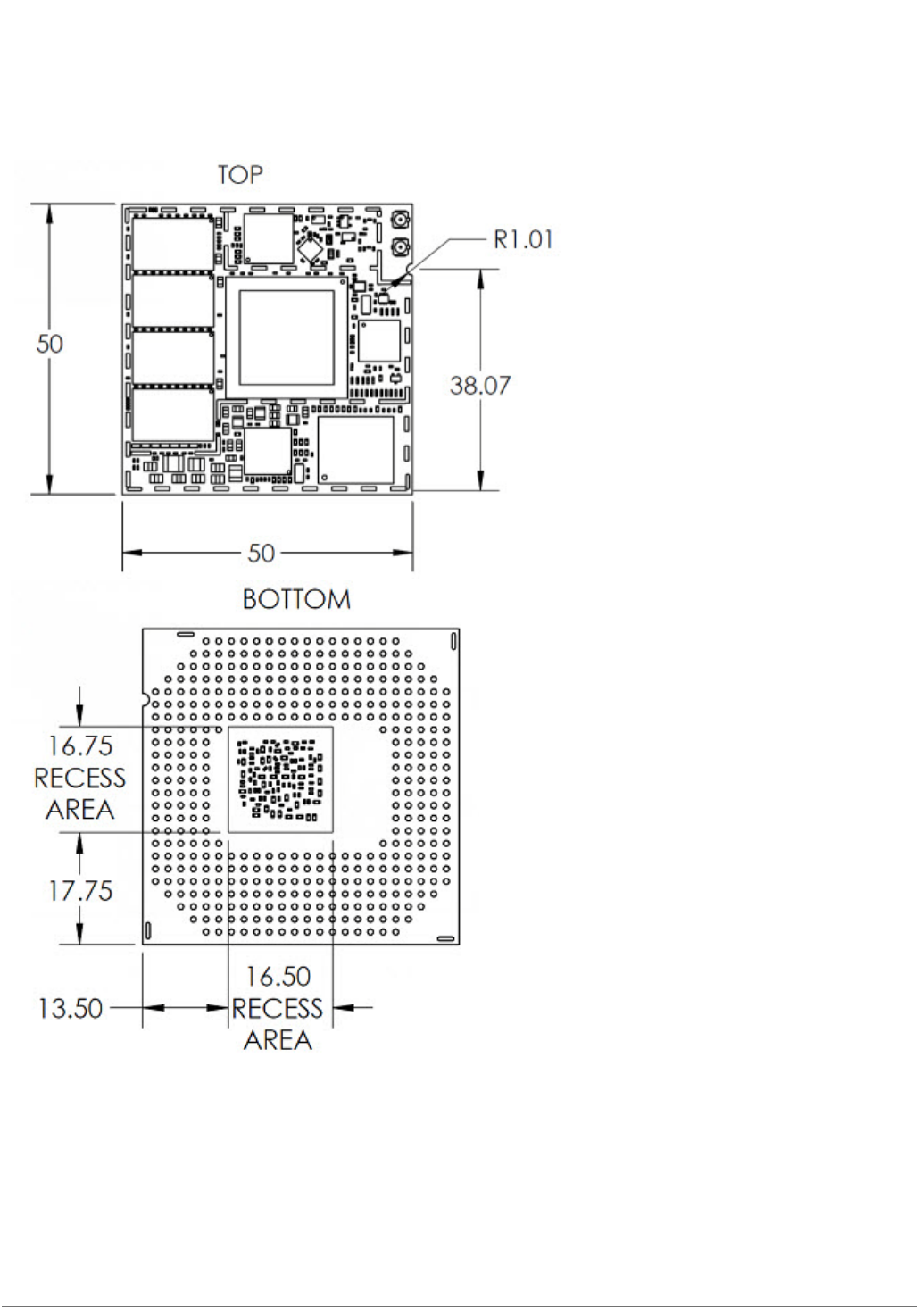
© 2014 Digi International Inc. 83
ConnectCore for i.MX6 Hardware Reference Manual
Module Specifications
Mechanical specifications
There must be a recess in the host PCB to accommodate the components on the bottom side of
the SOM. All dimensions are in millimeters.
Refer to Digi Application Note #31-31-14-x posted on the Digi technical support website for
additional information.
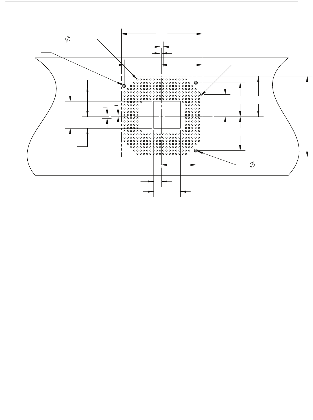
© 2014 Digi International Inc. 84
ConnectCore for i.MX6 Hardware Reference Manual
Host PCB Footprint
Note: Minimum thickness of the host board shall be 2mm.
R1
2
5
16.50
16.75
25
50
50
2 1
1
7.25
13.75 25
0.89
21.20
23.20
21
21
19
2
NON ROUTING AREA
(3X)

© 2014 Digi International Inc. 85
ConnectCore for i.MX6 Hardware Reference Manual
Specifications for the ConnectCore 6
Environmental Specifications
Operating temperatures stated below are Tj (i.MX6 junction temperatures) and are depending on
the actual processor population on the ConnectCore 6 module.
Industrial Variant: -40° C to +105° C
Extended Commercial Variant: -20° C to +105° C
Commercial Variant: 0° C to +95° C
The customer design must assure that the specified i.MX6 junction temperatures are not
exceeded during operation.
Storage temperature: -40°C to +85°C
Moisture Sensitivity and Shelf Life
a The ConnectCore for i.MX6 module is classified as a Level 3 Moisture Sensitive Device in
accordance with IPC/JEDEC J-STD-020.
b Calculated shelf life in sealed packaging: 12 months at <40°C and <90% relative humidity
(RH).
c Environmental condition during production: 30°C /60% RH according to IPC/JEDEC J-STD -
033A, paragraph 5.
d Maximum time between opening of the sealed packaging and reflow process must not exceed
168 hours, based on condition b), IPC/JEDEC J-STD -033A, paragraph 5.2.
e Baking is required, if conditions b) or c) do not apply. See above.
f Baking is required, if the packaging humidity indicator indicates 10% RH or higher.
g If baking is required, bake modules in trays 4-6 hours at 125°C; maximum stacking height is
10 trays.
Mounting
The ConnectCore 6 module has been designed with easy integration into existing SMT processes
in mind. Guidance for mounting the module on your carrier board is given in this section of the
document.
The ConnectCore 6 module is specified for one (1) soldering cycle only. Modules are also not
sealed and therefore they should not be subjected to a wash cycle or similar treatment where
condensation could occur. Contact Digi International for additional guidance to discuss conformal
coating approaches and options, if needed.Solder Paste
The following solder paste type has been approved for mounting the module on a carrier board:
• SAC305 (Lead-free: Alpha OM-340 Type 4 or equivalent)

© 2014 Digi International Inc. 86
ConnectCore for i.MX6 Hardware Reference Manual
Solder Paste Print
The following solder paste printing parameters are recommended:
• Stencil Thickness: 0.15 mm/5 mil
• Stencil Diameter: One to one of Pad diameter (to +20% of pad)
• Paste alignment: 20% off the pad max (offset <20% pad diameter)
Stencil
The recommendation is to use a laser cut and/or electro-formed stencil for placing the
ConnectCore 6 module. Based on the actual coplanarity characteristics of your carrier board,
adjustments may be required to determine the optimal solder paste volume.
It is also recommended to perform an X-ray analysis of the initial production run of your
assembly with the ConnectCore 6. Please contact Digi for additional support.
Coplanarity
The coplanarity measured on the ConnectCore for 6 is <0.001" bow and twist (98% confidence
interval). It is important that the carrier board is also coplanar. If the carrier board is thinner
than the ConnectCore 6 it is recommended that the assembly be supported during the reflow
process, i.e. reflow fixture should be used to minimize the potential bow of the carrier card.
SMT Pick and Place
• Placement Nozzle: Large is available on the machine
• Nozzle Pick Surface: Center of Shield on i.MX6 SOM
• Placement Speed: Slowest speed for the machine
• Placement alignment: 10% of pad diameter (compensating for module weight and supporting
alignment). The module should be placed last as part of the assembly/mounting process to
eliminate unexpected shifting.
SMT Process Parameter Reference
Process SMT process Specification recommendations
Screen print
Solder paste Leaded: Indium NC-SMQ92J / Lead-free: Alpha
OM-340
Stencil thickness 0.15mm / 5 mil
Stencil diameter 1.47mm / 58mil
Paster alignment 25% off the pad (offset <0.25* diameter
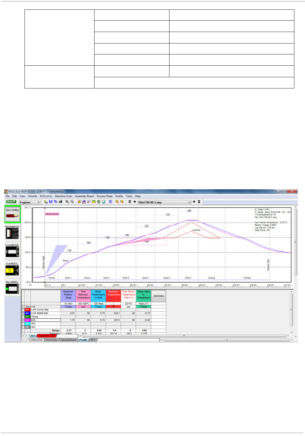
© 2014 Digi International Inc. 87
ConnectCore for i.MX6 Hardware Reference Manual
Reflow Profile Using Seven Zone Oven, SAC 305Lead-Free
Solder Paste (Alpha OM-340)
Time Above Liquidous (TAL) is recommended to be between 56 to 63 seconds. Use of 40AWG
K-type thermal couple and M.O.L.E or equivalent thermal profiler is recommended. The first
recommended thermal probe location is on the outer row of pads, to be on the out most row of
pins preferably a ground pad. The second thermal probe location is on the inner row of pads
preferably a signal pad.
The following image shows the reflow profile based on a seven zone convection oven.
The reflow profile shown above is valid for the combination solder paste/reflow machine and Digi
reference carrier board. Optimization of a reflow profile will depend on the selected solder paste/
reflow machine (reflow or vapor phase) and carrier board design.
PnP
Placement nozzle 0>15mm vacuum
Nozzle Pick Surface PnP cap center
Speed Slowest speed for the machine
Placement Sequence Place the SoM last
Placement Alignment 50% off the pad (offset <.5* diameter)
Reflow Belt speed 0.6-1.1 m/sec
Refer to SMT profile recommendation in the next page
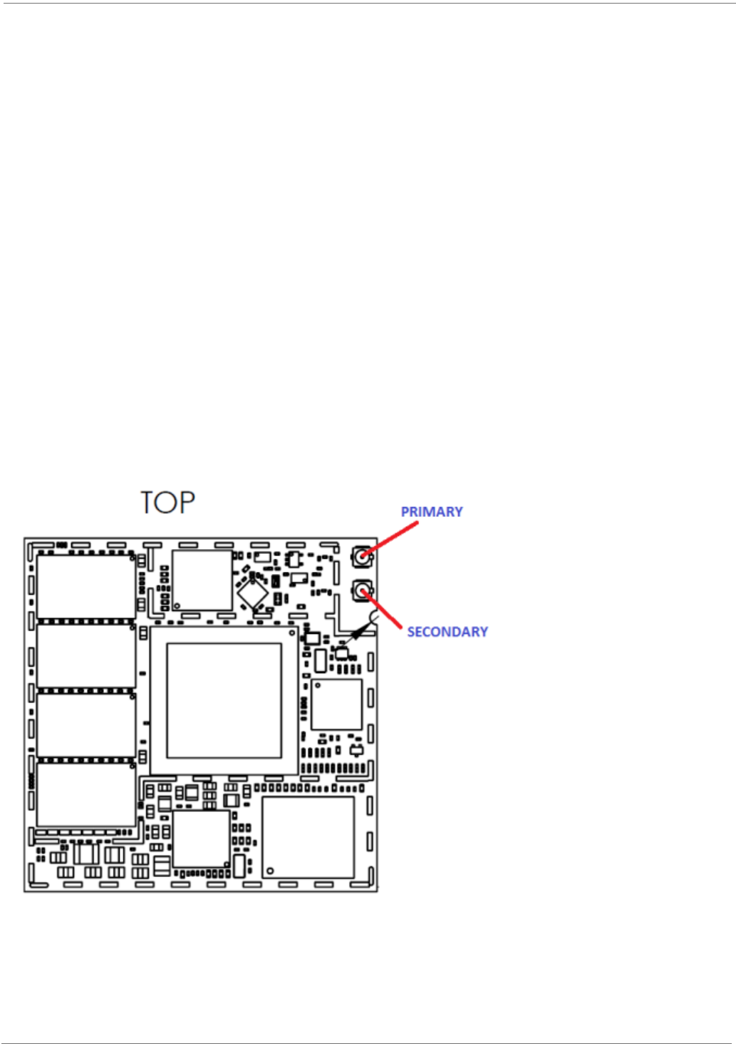
© 2014 Digi International Inc. 88
ConnectCore for i.MX6 Hardware Reference Manual
Network Interface
WLAN Standard:
• IEEE 802.11a/b/g/n standards
• HT20, and HT40 IEEE 802.11n
Frequency Band:
• 2.40-2.50 GHz (low band)
• 5.18-5.825 GHz (High band)
Data Rates:
• 802.11b: 1, 2, 5.5, 11 Mbps
• 802.11a/g: 6, 9, 12, 18, 24, 35, 48, 54 Mbps
• 802.11n HT20 FGI: 6.5, 13, 19.5, 26, 39, 52, 58.5, 65 Mbps
• 802.11n HT20 HGI: 7.2, 14.4, 21.7, 29.9, 43.3, 57.8, 65, 72.2 Mbps
• 802.11n HT40 FGI (5GHz only): 13.5, 27, 40.5, 54, 81, 108, 121.5, 135 Mbps
• 802.11n HT40 HGI (5GHz only): 15, 30, 45, 60, 90, 120, 135, 150 Mbps
Antenna ports:
Note: Modules with Bluetooth capabilities will not support spatial diversity.
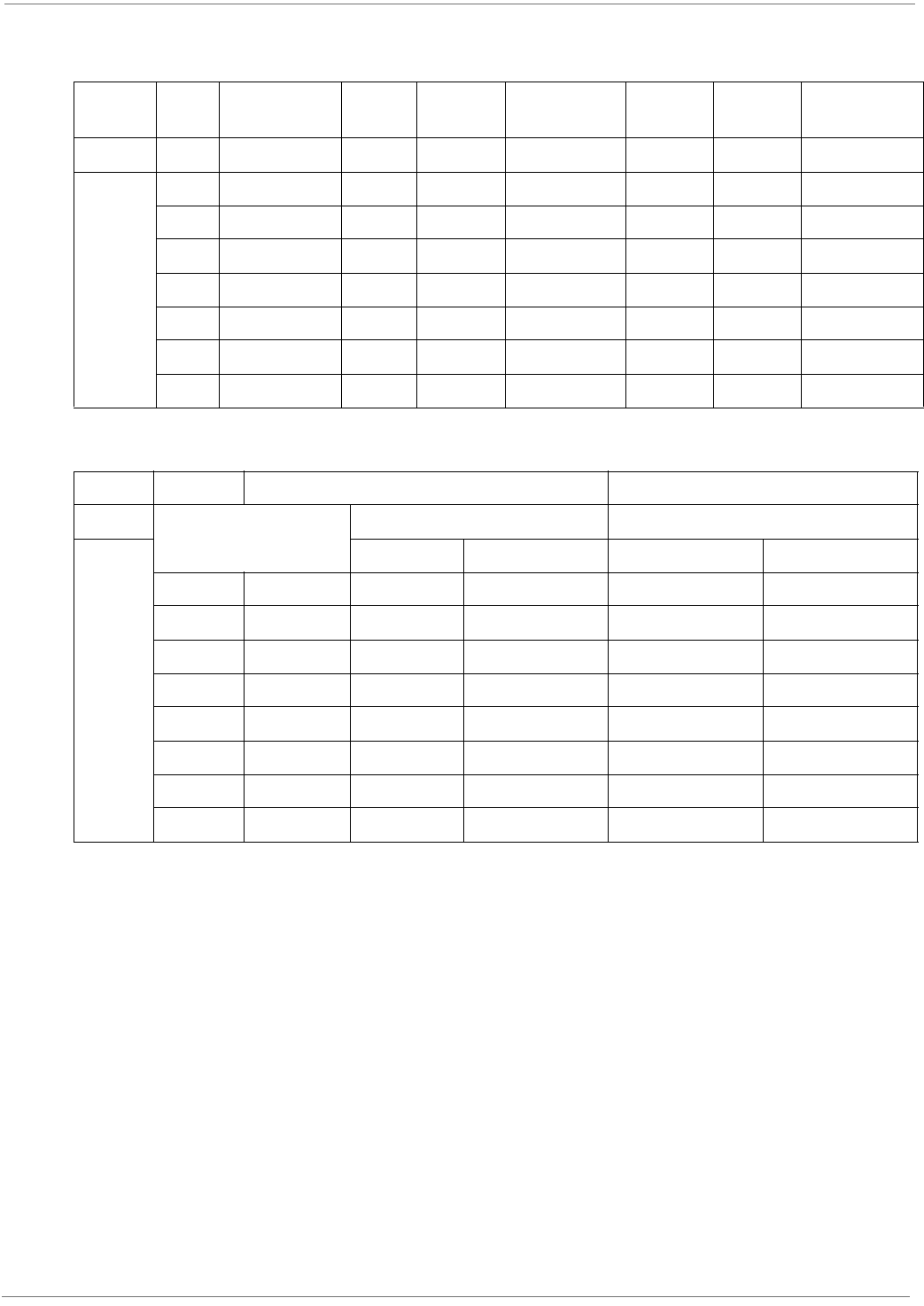
© 2014 Digi International Inc. 89
ConnectCore for i.MX6 Hardware Reference Manual
Modulation
Security/Interoperability
• WPA-PSK
• WPA-Enterprise
• WPA2-Personal
• WPA2-Enterprise
• Wi-Fi Direct
• Soft AP
• WAPI (optional, China)
• Cisco CCXv4 ASD certification ready (optional)
• Wi-Fi Alliance Logo certification ready
The listed capabilities are dependent on software platform in use. Refer to the corresponding
software platform documentation for additional information.
Mode Data
rate Modulation Mode Data
rate Modulation Mode Data
rate Modulation
802.11b 1 DBPSK 802.11g 6 BPSK 802.11a 6 BPSK
2 DQPSK 9 BPSK 9 BPSK
5.5 CCK 12 QPSK 12 QPSK
11 CCK 18 QPSK 18 QSPK
24 16-QAM 24 16-QAM
35 16-QAM 35 16-QAM
48 64-QAM 48 64-QAM
54 64-QAM 54 64-QAM
Mode MCS Modulation Data rate
802.11n HT20 (2.4 GHz and 5GHz) HT40 (5GHz only)
FGI HGI FGI HGI
MCS0 BPSK 6.5 7.2 13.5 15
MCS1 QPSK 13 14.4 27 30
MCS2 QPSK 19.5 21.7 40.5 45
MCS3 16-QAM 26 29.9 54 60
MCS4 16-QAM 39 43.3 81 90
MCS5 64-QAM 52 57.8 108 120
MCS6 64-QAM 58.5 65 121.5 135
MCS7 64-QAM 65 72.2 135 150

© 2014 Digi International Inc. 90
ConnectCore for i.MX6 Hardware Reference Manual
Please contact Digi if your end product requires a Wi-Fi Alliance Logo and/or Cisco CCX
certification.
Frequency Bands
US, Canada
• 2.412 to 2.462 GHz; 11 channels
• 5.180 to 5.320 GHz; 8 channels
• 5.500 to 5.700 GHz, 8 channels (excludes 5.600 to 5.650 GHz)
• 5.745 to 5.825 GHz; 5 channels
Europe
• 2.412 to 2.472 GHz; 13 channels
• 5.180 to 5.320 GHz; 8 channels
• 5.500 to 5.700 GHz, 8 channels (excludes 5.600 to 5.640 GHz)
Australia, New Zealand
• 2.412 to 2.462 GHz; 11 channels
• 5.180 to 5.320 GHz; 8 channels
• 5.745 to 5.825 GHz; 5 channels
Japan
• 2.412 to 2.472 GHz; 13 channels
• 5.180 to 5.320 GHz; 8 channels
• 5.500 to 5.700 GHz; 11 channels
Ad-Hoc Mode Channels
• 2.4GHz Band - Channels 10 and 11
• 5GHz Band US, Australia, New Zealand - Channels 36, 40, 44, 45, 149, 157, 161, and 165
Channels 36, 40, 44, and 45 are for indoor use only
• 5GHz Band Europe and Japan - per 802.11d
5GHz HT20 and HT40 channel available:
Channel number Frequency (MHz) Mode Secondary channel allowed
36 5180 HT40 PLUS
38 5190 HT20
40 5200 HT40 MINUS
44 5220 HT40 PLUS
46 5230 HT20

© 2014 Digi International Inc. 91
ConnectCore for i.MX6 Hardware Reference Manual
Receive Sensitivity
48 5240 HT40 MINUS
52 5260 HT40 PLUS
54 5270 HT20
56 5280 HT40 MINUS
60 5300 HT40 PLUS
62 5310 HT20
64 5320 HT40 MINUS
100 5500 HT40 PLUS
102 5510 HT20
104 5520 HT40 MINUS
108 5540 HT40 PLUS
110 5550 HT20
112 5560 HT40 MINUS
116 5580 HT40 PLUS
118 5590 HT20
120 5600 HT40 MINUS
124 5620 HT40 PLUS
126 5630 HT20
128 5640 HT40 MINUS
132 5660 HT40 PLUS
134 5670 HT20
136 5680 HT40 MINUS
140 5700 HT20
159 5745 HT40 PLUS
151 5755 HT20
153 5765 HT40 MINUS
157 5785 HT40 PLUS
159 5795 HT20
161 5805 HT40 MINUS
165 5825 HT20
Network type Sensitivity
802.11b -88 dBm
802.11g -88 dBm
802.11n (2.4GHz) -89 dBm
802.11a -90 dBm
802.11n (5GHz, HT20) -90 dBm
802.11n (5GHz, HT40) -86 dBm

© 2014 Digi International Inc. 92
ConnectCore for i.MX6 Hardware Reference Manual
Transmit Power
Bluetooth
• Bluetooth 3.0 + HS (BT3.0 + HS)
• Bluetooth 4.0 (BT4.0)
• Class 1.5 Bluetooth with integrated TX/RX switch
Electrical Characteristics
Voltage supplies
Note: No specific ESD protection components have been implemented on the ConnectCore
for i.MX6 module. ESD protection level on the module’s I/Os is the same as what is specified
in the freescale datasheet. Any required ESD protection must be implemented on the carrier
board.
Network type Transmit power
802.11b 10.5 dBm
802.11g/n 11 dBm
802.11a/n 13 dBm
Parameter Min Typ Max Unit
5V supply 4.2 5 5.5 V
VCC_LICELL 2.0 3.0 TBD V
LDO3_MCA 1.71 3.3 3.6 V
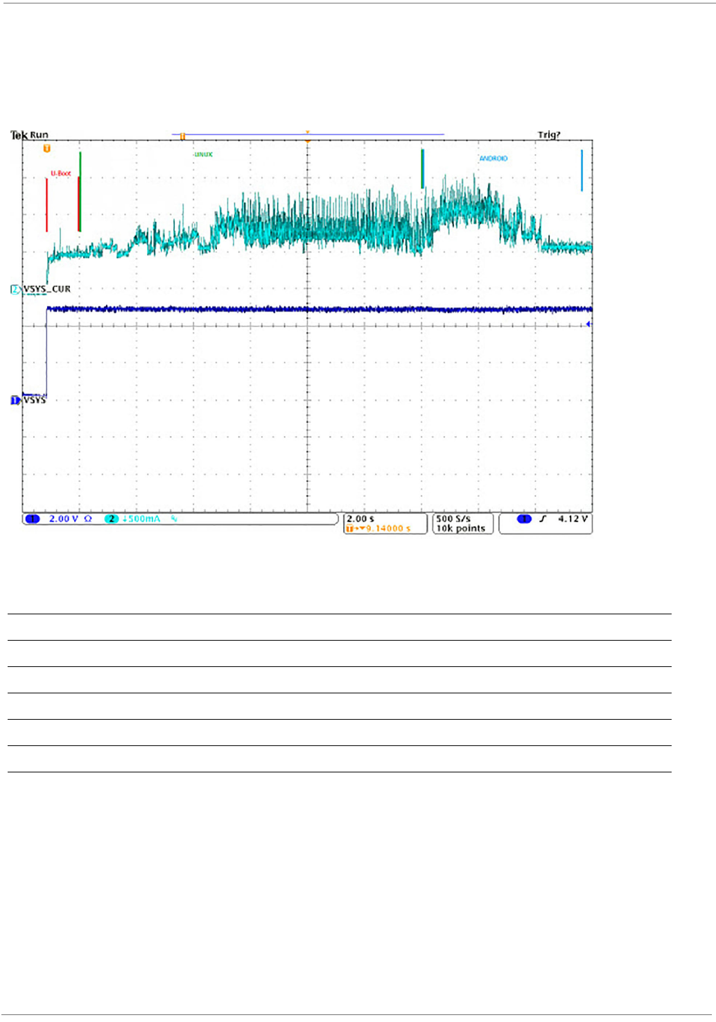
© 2014 Digi International Inc. 93
ConnectCore for i.MX6 Hardware Reference Manual
Power Consumption
The following image displays the current consumption of the ConnectCore for i.MX6 module
when booting respectively through U-Boot, Linux kernel and Android user space.
Power consumption of the ConnectCore 6
Agency Approval
Specification ConnectCore for i.MX6
United States (FCC Part 15.247) Pending
Industry Canada (IC) Pending
Europe (DC) Pending
Japan Pending
Australia Pending
© 2014 Digi International Inc. 94
ConnectCore for i.MX6 Hardware Reference Manual
Certifications
Agency Certifications
United States FCC
The ConnectCore™ for i.MX6 Module complies with Part 15 of the FCC rules and regulations.
Compliance with the labeling requirements, FCC notices and antenna usage guidelines is
required. To fulfill FCC Certification, the OEM must comply with the following regulations:
• The system integrator must ensure that the text on top side of the module is placed on the
outside of the final product.
• ConnectCore™ for i.MX6 Module may only be used with antennas approved [refer to the
antenna tables in this section].
For WiFi/Bluetooth variant:
For WiFi only variant:
FCC Notices
IMPORTANT: The ConnectCore™ for i.MX6 module has been certified by the FCC for use with
other products without any further certification (as per FCC section 2.1091). Modifications not
expressly approved by Digi could void the user's authority to operate the equipment.
IMPORTANT: OEMs must test final product to comply with unintentional radiators (FCC section
15.107 & 15.109) before declaring compliance of their final product to Part 15 of the FCC Rules.
WARNING: The Original Equipment Manufacturer (OEM) must ensure that FCC
labeling requirements are met. This includes a clearly visible label on the outside of the
final product enclosure that displays the contents shown in the figure below. Required
FCC Label for OEM products containing the ConnectCore™ for i.MX6 Module.
Contains FCC ID: MCQ-CCIMX6B
This device complies with part 15 of the FCC Rules. Operation is subject to the
following two conditions: (1) This device may not cause harmful interference, and
(2) this device must accept ant interference received, including interference that
may cause undesired operation.
Contains FCC ID: MCQ-CCIMX6
This device complies with part 15 of the FCC Rules. Operation is subject to the
following two conditions: (1) This device may not cause harmful interference, and
(2) this device must accept ant interference received, including interference that
may cause undesired operation.

© 2014 Digi International Inc. 95
ConnectCore for i.MX6 Hardware Reference Manual
IMPORTANT: The ConnectCore™ for i.MX6 module has been certified for remote and base radio
applications. If the module will be used for portable applications, the device must undergo SAR
testing. This equipment has been tested and found to comply with the limits for a Class B digital
device, pursuant to Part 15 of the FCC Rules. These limits are designed to provide reasonable
protection against harmful interference in a residential installation. This equipment generates
uses and can radiate radio frequency energy, and if not installed and used in accordance with
the instructions, may cause harmful interference to radio communications. However, there is no
guarantee that interference will not occur in a particular installation. If this equipment does
cause harmful interference to radio or television reception, which can be determined by turning
the equipment off and on, the user is encouraged to try to correct the interference by one or
more of the following measures: Re-orient or relocate the receiving antenna, Increase the
separation between the equipment and receiver, Connect equipment and receiver to outlets on
different circuits, or Consult the dealer or an experienced radio/TV technician for help.
FCC-Approved Antennas
The ConnectCore™ for i.MX6 can be installed utilizing antennas and cables constructed with non-
standard connectors (RPSMA, RPTNC, and so on).
The modules are FCC approved for fixed base station and mobile applications for the channels
indicated in the tables below. If the antenna is mounted at least 20cm (8 in.) from nearby
persons, the application is considered a mobile application. Antennas not listed in the table must
be tested to comply with FCC Section 15.203 (Unique Antenna Connectors) and Section 15.247
(Emissions).
The antennas in the tables below have been approved for use with this module. Digi does not
carry all of these antenna variants. Contact Digi Sales for available antennas.
Antennas Approved for Use with the ConnectCore™ for i.MX6 Wi-Fi Modules
Note: If using the RF module in a portable application (for example - if the module is used
in a hand-held device and the antenna is less than 20cm from the human body when the
device is in operation): The integrator is responsible for passing additional SAR (Specific
Absorption Rate) testing based on FCC rules 2.1091 and FCC Guidelines for Human Exposure
to Radio Frequency Electromagnetic Fields, OET Bulletin and Supplement C. The testing
results will be submitted to the FCC for approval prior to selling the integrated unit. The
required SAR testing measures emissions from the module and how they affect the person.
Omni- directional antennas
Part number Type (description) Peak Gain 2.4 GHz Peak Gain 5 GHz
Digi International
A24-HASM-450
Dipole (articulated RPSMA,
2.4GHz antenna) 1.8dBi
Linx Technologies Inc
ANT-DB1-RAF-RPS
Dipole (articulated RPSMA,
2.4GHz and 5GHz antenna) 2.5dBi 4.6dBi
Yageo
ANTX100P001B24003 2.4GHz PCB antenna
4dBi (@2.4GHz)
4.4dBi (@2.45GHz)
4.1dBi (@2.5GHz)
Ethertronics 1001932 2.4 - 5GHz PCB antenna 1.5-2.5dBi 3-5dBi
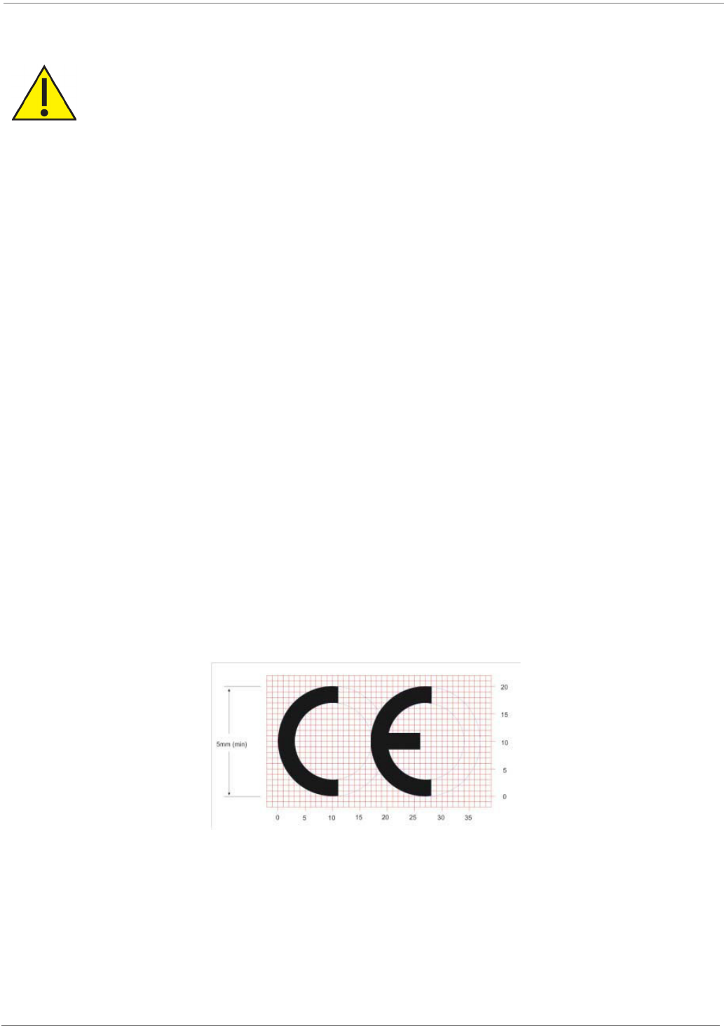
© 2014 Digi International Inc. 96
ConnectCore for i.MX6 Hardware Reference Manual
RF Exposure
Europe (ETSI)
The ConnectCore™ for i.MX6 Module has been certified for use in several European countries.
For a complete list, refer to www.digi.com.
If the ConnectCore™ for i.MX6 module is incorporated into a product, the manufacturer must
ensure compliance of the final product to the European harmonized EMC and low-voltage/safety
standards. A Declaration of Conformity must be issued for each of these standards and kept on
file as described in Annex II of the R&TTE Directive.
Furthermore, the manufacturer must maintain a copy of the ConnectCore™ for i.MX6 Hardware
Reference manual documentation and ensure the final product does not exceed the specified
power ratings, antenna specifications, and/or installation requirements as specified in the user
manual. If any of these specifications are exceeded in the final product, a submission must be
made to a notified body for compliance testing to all required standards.
OEM Labeling Requirements
The CE marking must be affixed to a visible location on the OEM product.
CE Labeling Requirements
The CE mark shall consist of the initials CE taking the following form:
• If the CE marking is reduced or enlarged, the proportions given in the above graduated
drawing must be respected.
• The CE marking must have a height of at least 5mm except where this is not possible on
account of the nature of the apparatus.
• The CE marking must be affixed visibly, legibly, and indelibly.
WARNING: To satisfy FCC RF exposure requirements for mobile transmitting devices,
a separation distance of 20 cm or more should be maintained between the antenna of
this device and persons during device operation. To ensure compliance, operations at
closer than this distance are not recommended. The antenna used for this transmitter
must not be co-located in conjunction with any other antenna or transmitter. The
preceding statement must be included as a CAUTION statement in OEM product
manuals in order to alert users of FCC RF Exposure compliance.

© 2014 Digi International Inc. 97
ConnectCore for i.MX6 Hardware Reference Manual
Declarations of Conformity
Digi has issued Declarations of Conformity for the ConnectCore™ for i.MX6 module concerning
emissions, EMC and safety. Files can be obtained by contacting Digi Support.
Note: Digi does not list the entire set of standards that must be met for each country. Digi
customers assume full responsibility for learning and meeting the required guidelines for each
country in their distribution market.
Approved Antennas
The same antennas have been approved for Europe as stated in the FCC table for use with the
ConnectCore™ for i.MX6 module.
Canada (IC)
This device complies with Industry Canada license-exempt RSS standard(s). Operation is subject
to the following two conditions: (1) this device may not cause interference, and (2) this device
must accept any interference, including interference that may cause undesired operation of the
device.
Le présent appareil est conforme aux CNR d'Industrie Canada applicables aux appareils radio
exempts de licence. L'exploitation est autorisée aux deux conditions suivantes : (1) l'appareil ne
doit pas produire de brouillage, et (2) l'utilisateur de l'appareil doit accepter tout brouillage
radioélectrique subi, même si le brouillage est susceptible d'en compromettre le fonctionnement.
Labeling Requirements
Labeling requirements for Industry Canada are similar to those of the FCC. A clearly visible label
on the outside of the final product enclosure must display the following text:
For WiFi/Bluetooth variant:
For WiFi only variant:
The integrator is responsible for its product to comply with IC ICES-003 & FCC Part 15, Sub. B -
Unintentional Radiators. ICES-003 is the same as FCC Part 15 Sub. B and Industry Canada
accepts FCC test report or CISPR 22 test report for compliance with ICES-003.
Transmitters with Detachable Antennas
This radio transmitter (IC: 1846A-CCIMX6 / IC: 1846A-CCIMX6B) has been approved by Industry
Canada to operate with the antenna types listed in the table above with the maximum
permissible gain and required antenna impedance for each antenna type indicated. Antenna
types not included in this list, having a gain greater than the maximum gain indicated for that
type, are strictly prohibited for use with this device.
Contains Model ConnectCoreTM for i.MX6 Radio, IC: 1846A-CCIMX6B
Contains Model ConnectCoreTM for i.MX6 Radio, IC: 1846A-CCIMX6

© 2014 Digi International Inc. 98
ConnectCore for i.MX6 Hardware Reference Manual
Le présent émetteur radio (IC: 1846A-CCIMX6 / IC: 1846A-CCIMX6B) a été approuvé par
Industrie Canada pour fonctionner avec les types d'antenne énumérés ci-dessous et ayant un
gain admissible maximal et l'impédance requise pour chaque type d'antenne. Les types
d'antenne non inclus dans cette liste, ou dont le gain est supérieur au gain maximal indiqué, sont
strictement interdits pour l'exploitation de l'émetteur.
Under Industry Canada regulations, this radio transmitter may only operate using an antenna of
a type and maximum (or lesser) gain approved for the transmitter by Industry Canada. To
reduce potential radio interference to other users, the antenna type and its gain should be so
chosen that the equivalent isotropically radiated power (e.i.r.p.) is not more than that necessary
for successful communication.
Conformément à la réglementation d'Industrie Canada, le présent émetteur radio peut
fonctionner avec une antenne d'un type et d'un gain maximal (ou inférieur) approuvé pour
l'émetteur par Industrie Canada. Dans le but de réduire les risques de brouillage radioélectrique
à l'intention des autres utilisateurs, il faut choisir le type d'antenne et son gain de sorte que la
puissance isotrope rayonnée équivalente (p.i.r.e.) ne dépasse pas l'intensité nécessaire à
l'établissement d'une communication satisfaisante.
Japan
こ の製品は、 周波数帯域 5.15 ~ 5.35 GHz で動作しているときは、 屋内においてのみ使⽤可能です。
This device has been granted a designation number by Ministry of Internal Affairs and
Communications according to:
Ordinance concerning Technical Regulations Conformity Certification etc. of Specified Radio
Equipment ( 特定無線設備の技術基準適合証明等に関す る規則 ).
• Article 2 clause 1 item 19 Approval n°: TBD
• Article 2 clause 1 item 19 (2) Approval n°: TBD
• Article 2 clause 1 item 19 (3) Approval n°: TBD
• Article 2 clause 1 item 19 (3) (2) Approval n°: TBD
This device should not be modified (otherwise the granted designation number will be invalid).