Digianswer A S 13192-EVB WPAN Transceiver User Manual Manual
Digianswer A/S WPAN Transceiver Manual
Contents
- 1. Quick start guide
- 2. Manual
Manual

MC13192
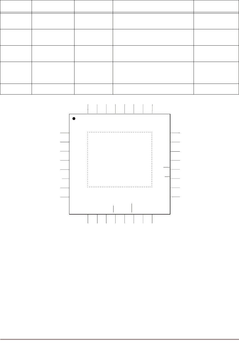
Ordering Information
Device Device Marking Package
MC13192 13192 QFN-32
Package Information
Plastic Package
Case 1311-03
(QFN-32)
(Scale 1:1)
This document contains information on a product under development.
Motorola reserves the right to change or discontinue this product without notice. © Motorola,Inc.,2004.All rights
The MC13192 is a short range, low power, 2.4 GHz ISM band transceiver which contains a
complete 802.15.4 physical layer (PHY) modem designed for the IEEE 802.15.4 wireless
standard supporting star and mesh networking.
When combined with an appropriate microcontroller (MCU), the MC13192 provides a cost
effective solution for short-range data links and networks. Interface with the MCU is
accomplished utilizing a four wire serial peripheral interface (SPI) connection which allows
for the use of a variety of processors. The software and processor can be scaled to fit
applications ranging from simple point-to-point systems, through complete ZigBee™
networking.
For more detailed information on MC13192 operation, refer to the MC13192 Reference
Manual, part number MC13192RM/D.
Applications include, but are not limited to, the following:
• Remote control and wire replacement in industrial systems such as wireless sensor
networks
• Factory automation and motor control
• Heating and cooling
• Inventory management and RF ID tagging
Potential consumer applications include:
• Home automation and control
• Human interface devices
• Remote entertainment control
Product Preview
MC13192/D
Rev. 2.4, 06/2004
2.4 GHz, Low Power
Transceiver for 802.15.4
Contents
1 Features . . . . . . . . . . . . . 2
2 Block Diagrams . . . . . . . 3
3 Data Transfer Modes . . 3
4Electrical
Characteristics . . . . . . . 5
5Functional
Description . . . . . . . . . . 8
6 Contact
Connections . . . . . . . . 11
7 Applications
Information . . . . . . . . . . 15
8 Packaging
Information . . . . . . . . . . 18
Freescale Semiconductor, I
Freescale Semiconductor, Inc.
nc...

2MC13192 Product Preview MOTOROLA
Features
• Wireless toys
The transceiver includes a low noise amplifier, 1.0 mW PA, VCO, full spread-spectrum encoding and
decoding. The device supports 250 kbps O-QPSK data in 5.0 MHz channels, per the IEEE 802.15.4
specification. A Serial Peripheral Interface (SPI) is used for RX and TX data transfer and control.
1 Features
• Recommended power supply range: 2.0 to 3.4 V
• 16 Channels
• 0 dBm (Typical), up to 3.6 dBm maximum output power
• Buffered Transmit and Receive Data Packets for Simplified Use with Low Cost Microcontrollers
• Supports 250 kbps O-QPSK Data in 5.0 MHz Channels and Full Spread-Spectrum Encode and
Decode (Compatible with IEEE Standard 802.15.4)
• Three Power Down Modes for Power Conservation:
— < 1 µA Off Current
— 3.0 µA Typical Hibernate Current
— 40 µA Typical Doze Current
• RX sensitivity of -92 dBm (Typical) at 1.0% Packet Error Rate
• Four internal timer comparators are available to reduce MCU resource requirements
• Clock output is available for use by MCU
• Seven General Purpose Input/Output ports (GPIO) are available
• Operating Temperature Range: -40°C to 85°C
• Small form factor QFN-32 Package
— Meets Moisture Sensitivity Level (MSL) 3
— 260°C Peak Reflow temperature
— Meets lead-free requirements
Freescale Semiconductor, I
Freescale Semiconductor, Inc.
nc...

Block Diagrams
MOTOROLA MC13192 Product Preview 3
2 Block Diagrams
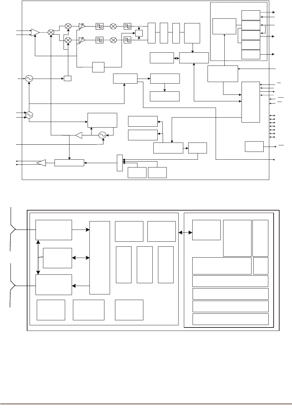
Figure 1 shows a simplified block diagram of the MC13192. The MC13192 is an IEEE 802.15.4
transceiver that provides most of the functions required in the Physical Layer (PHY) specification.
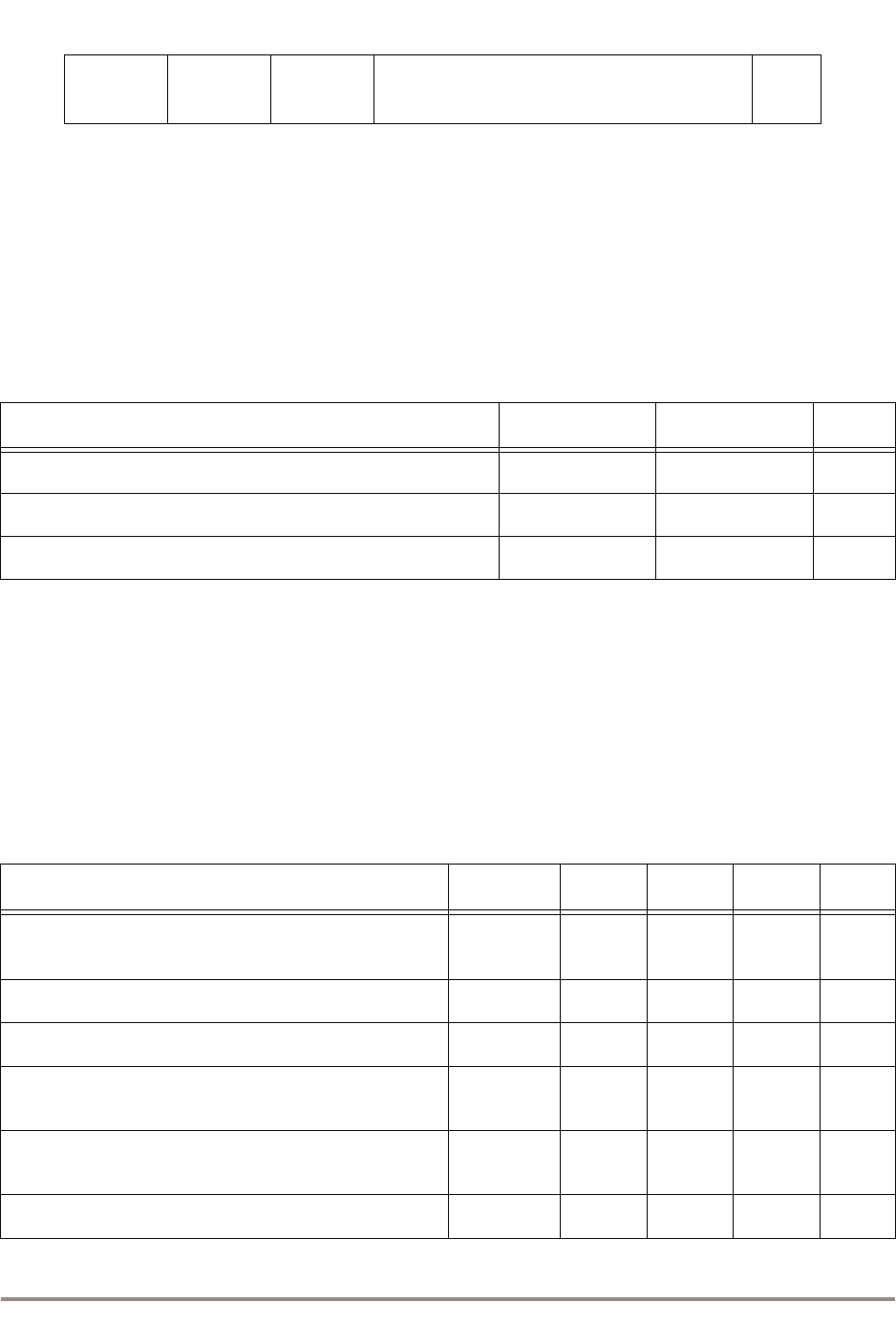
Figure 2 shows the basic system block diagram for the MC13192 in an application. Interface with the IC is
accomplished through a 4-wire Serial Peripheral Interface (SPI). The Medium Access Control (MAC),
drivers, and Network and Application software as required reside on the host processor. The host can be
anything from a simple 8-bit device up to a sophisticated 32-bit processor depending on application
requirements.
3 Data Transfer Modes
The MC13192 has two data transfer modes:
1. Packet Mode — Data is buffered in on-chip RAM
2. Streaming Mode — Data is processed word by word
When using the Motorola 802.15.4 MAC, only the streaming mode can be used. For proprietary
applications, packet mode is used to conserve MCU resources.
3.1 Packet Structure
Figure 3 shows the packet structure of the MC13192. Payloads of up to 125 bytes are supported. The
MC13192 adds a four byte preamble, a one byte start of frame delimiter (SFD), and a one byte frame
length indicator before the data. A Frame Check Sequence (FCS) is calculated and appended to the end of
the data.
3.2 Receive Path Description
In the receive signal path, the RF input is converted to low IF In-phase and Quadrature (I & Q) signals
through two down conversion stages. A Clear Channel Assessment (CCA) can be performed based on the
baseband energy integrated over a specific time interval. The digital back end performs Differential Chip
Detection (DCD), the correlator “de spreads” the Direct Sequence Spread Spectrum (DSSS) Offset QPSK
(O-QPSK) signal, determines the symbols and packets, and detects the data.
The preamble, SFD, and frame length are parsed and used. A two-byte FCS is calculated and compared to
the FCS value appended to the transmitted data, generating a Cyclical Redundancy Check (CRC) result.
Link Quality is measured over a 64 µs period after the packet preamble and stored in ROM.
If the MC13192 is in packet mode, the data is processed as an entire packet. The MCU is notified that an
entire packet has been received via an interrupt.
If the MC13192 is in streaming mode, the MCU is notified by an interrupt on a word by word basis.
3.3 Transmit Path Description
The transmit path is the exact reverse of the receive path. The data stored in RAM is retrieved or clocked in
via the SPI, formed into packets per the 802.15.4 PHY, spread, and then up converted to the transmit
frequency.
If the MC13192 is in packet mode, data is processed as an entire packet. The data is loaded into the TX
buffer. The MCU then requests that the MC13192 transmit the data. The MCU is notified that the whole
packet has successfully been transmitted via an interrupt.
Freescale Semiconductor, I
Freescale Semiconductor, Inc.
nc...
4MC13192 Product Preview MOTOROLA
Data Transfer Modes
In streaming mode, the data is fed to the MC13192 on a word by word basis with an interrupt serving as a
notification that the MC13192 is ready for more data. This continues until the whole packet is transmitted.
Figure 1. MC13192 Simplified Block Diagram
Figure 2. System Level Block Diagram
Phase Shift Modulator
RST
GPIO1
GPIO2
GPIO3
GPIO4
Crystal2
Crystal1
RFIN-
RFIN+
PAO+
PAO-
MOSI
MISO
SPICLK
RXTXEN
CE
ATTN
GPIO5
GPIO6
GPIO7
Receive
Packet RAM
Transmit
Packet RAM 1
Transmit RAM
Arbiter
Receive RAM
Arbiter
PA
VCO
Crystal
Oscillator
Symbol
Generation
FCS
Generation Header
Generation
MUX
Sequence
Manager
(Control Logic)
VDDLO2 ÷4
256MHz
2.45GHz
LNA 1st IF Mixer
IF = 65 MHz
2nd IF Mixer
IF = 1 MHz PMA Decimation
Filter Matched
Filter
Baseband
Mixer
DCD
Correlator
Symbol
Synch & Det
CCA Packet
Processor
IRQ
Arbiter
24 Bit Event Timer
IRQ
16MHz
AGC
Analog
Regulator VBATT
Digital
Regulator L
Digital
Regulator H
Power-Up
Control
Logic
Crystal
Regulator
VCO
Regulator
VDDINT
Programmable
Prescaler
CLKO
4 Programmable
Timer Comparators
Synthesizer
VDDD
VDDVCO
SERIAL
PERIPHERAL
INTERFACE
(SPI)
VDDA
VDDLO1
Transmit
Packet RAM 2
Analog Receiver
MC13192
Frequency
Generation
Analog
Transmitter
Voltage
Regulators Power Up
Management
Control
Logic
Buffer RAM
Digital Transceiver
SPI
and GPIO
Microcontroller
SPI Rom (Flash)
RAM
CPU A/D
Timer
Application
IRQ Arbiter
RAM Arbiter
Timer
Network
MAC
PHY Driver
Freescale Semiconductor, I
Freescale Semiconductor, Inc.
nc...
Electrical Characteristics
MOTOROLA MC13192 Product Preview 5
Figure 3. MC13192 Packet Structure
4 Electrical Characteristics
4.1 Maximum Ratings
4.2 Recommended Operating Conditions
Table 1. Maximum Ratings
Rating Symbol Value Unit
Power Supply Voltage VBATT, VDDINT 3.6 Vdc
Junction Temperature TJ125 °C
Storage Temperature Range Tstg -55 to 125 °C
Note: Maximum Ratings are those values beyond which damage to the device may occur.
Functional operation should be restricted to the limits in the Electrical Characteristics
or Recommended Operating Conditions tables.
Note: Meets Human Body Model (HBM) = 2 kV and Machine Model (MM) = 200 V except RFin = 100 V MM,
PAout = 50 V MM & 1 kV HBM, and VBATT = 100 V MM. RF pins have no ESD protection including PAO+
and PAO -.
Table 2. Recommended Operating Conditions
Characteristic Symbol Min Typ Max Unit
Power Supply Voltage VBATT,
VDDINT
2.0 2.7 3.4 Vdc
Input Frequency fin 2.405 - 2.480 GHz
Ambient Temperature Range TA-40 25 85 °C
Logic Input Voltage Low Vil 0-30%
VDDINT
V
Logic Input Voltage High Vih 70%
VDDINT
-V
DDINT V
SPI Clock Rate fSPI --8.0MHz
Preamble
Start of
Frame
Delimiter
Frame
Length Payload FCS
4 bytes 1 byte 1 byte 125 bytes Max 2 bytes
Freescale Semiconductor, I
Freescale Semiconductor, Inc.
nc...

6MC13192 Product Preview MOTOROLA
Electrical Characteristics
4.3 DC Electrical Characteristics
RF Input Power Pmax --200dBm
Crystal Reference Oscillator Frequency (±40 ppm over
everything to meet the 802.15.4 standard.)
fref 16 MHz Only
Table 3. DC Electrical Characteristics
(VCC = 2.7 V, TA = 25°C, unless otherwise noted)
Characteristic Symbol Min Typ Max Unit
Power Supply Current (VBATT + VDDINT)
Off
Hibernate
Doze (No CLKO)
Idle
Transmit Mode
Receive Mode
Ileakage
ICCH
ICCD
ICCI
ICCT
ICCR
-
-
-
-
-
-
<1.0
3.0
40
500
34
37
-
-
-
-
-
-
µA
µA
µA
µA
mA
mA
Input Current Low (Vin = 0V) Iil - -1.0 - µA
Input Current High (Vin = VDDINT)I
ih -1.0-µA
Output High Voltage Voh 80%
VDDINT
-V
DDINT V
Output Low Voltage Vol 0-20%
VDDINT
V
Table 2. Recommended Operating Conditions (Continued)
Characteristic Symbol Min Typ Max Unit
Freescale Semiconductor, I
Freescale Semiconductor, Inc.
nc...
Electrical Characteristics
MOTOROLA MC13192 Product Preview 7
4.4 AC Electrical Characteristics
Table 4. Receiver AC Electrical Characteristics
Characteristic Symbol Min Typ Max Unit
Sensitivity for 1% Packet Error Rate (PER) SENSper --92-dBm
Saturation (maximum input level) SENSmax 0dBm
Adjacent Channel Interference for 1% PER (desired
signal -82 dBm)
-23-dB
Alternate Channel Interference for 1% PER (desired
signal -82 dBm)
-35-dB
Frequency Error Tolerance - - 200 kHz
Symbol Rate Error Tolerance - 80 ppm
In-band Spurious Reception - 28 - dB
Table 5. Transmitter AC Electrical Characteristics
Characteristic Symbol Min Typ Max Unit
Nominal Output Power Pout -0-dBm
Error Vector Magnitude EVM 27 %
Power Control Range - 20 - dB
Over the Air Data Rate Tbit - 250 - kbps
Freescale Semiconductor, I
Freescale Semiconductor, Inc.
nc...
8MC13192 Product Preview MOTOROLA
Functional Description
5 Functional Description
5.1 MC13192 Operational States
The MC13192 has a number of operational states that allow for low-current operation. Entry from the Off
to Idle state occurs when RST is de-asserted. Once in Idle, the SPI is active and controls the IC. Transition
to Off, Hibernate, and Doze is controlled through the SPI. These states are summarized, along with the
transition times, in Table 6. Current drain in the various states is listed in Table 3, DC Electrical
Characteristics.
Table 6. MC13192 Mode Definitions and Transition Times
Mode Definition Transition Time
To or From Idle
Off All IC functions Off, Leakage only. RST asserted. 23.332 ms to Idle
Hibernate Crystal Reference Oscillator Off. (SPI not functional.) IC Responds to
ATTN.
18.332 ms to Idle
Doze Crystal Reference Oscillator On but CLKO output available only if
Register 7, Bit 9 = 1 for frequencies of 1 MHz or less. (SPI not
functional.) Responds to ATTN and can be programmed to enter Idle
State through an internal timer comparator.
332 µs to Idle
Idle Crystal Reference Oscillator On with CLKO output available. SPI active.
Receive Crystal Reference Oscillator On. Receiver On. SPI should not be
accessed.
144 µs from Idle
Transmit Crystal Reference Oscillator On. Transmitter On. SPI should not be
accessed.
144 µs from Idle
Freescale Semiconductor, I
Freescale Semiconductor, Inc.
nc...
Functional Description
MOTOROLA MC13192 Product Preview 9
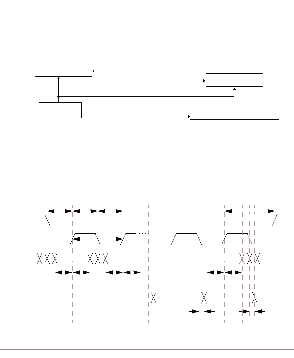
5.2 Serial Peripheral Interface (SPI)
Control of the MC13192 and data transfers are accomplished by means of a 4-wire Serial Peripheral
Interface (SPI). This section details the operation of the SPI.
5.2.1 General
The MC13192 operates as a slave device only. Data to be written into the IC is presented on the Master
Out/Slave In (MOSI) pin of the device, while data read from the device is presented to the master device
on the Master In/Slave Out (MISO) pin. Synchronization of the data is accomplished by the return-to-zero
Serial Clock (SPICLK) input and is framed by the Chip Enable (CE) pin. Data on MOSI is always clocked
into the IC on the leading edge of SPICLK and data is clocked out of the IC at MISO on the falling edge of
SPICLK. The master device should transfer MISO data to its internal registers on the trailing edge of
SPICLK. A typical interconnection to a microprocessor is shown in Figure 4.
Figure 4. SPI Interface
MISO is an active output and as such, does not enter a high impedance state at any time regardless of the
state of CE.
Although the SPI is fully static, internal memory, timer and interrupt arbiters require an internal clock,
CLKcore, derived from the crystal reference oscillator, to communicate from the SPI registers to internal
registers and memory.
Figure 5 and Table 7 show the SPI timing diagram and timing specifications.
Figure 5. SPI Parametric Timing Diagram.
Shift Register
Baud Rate
Generator
Shift Register
Chip Enable (CE)
RxD MISO
TxD MOSI
Sclk SPICLK
MCU MC13192
CE
MISO
SPICLK
CE
tPER
tCLKH tCLKL
tCE_SU
MOSI Addr 1R/W
Read 0
tSU tH
tSU tH
tP1 tP1
Write 0
Read 1
tCE_H
tSU tH
Freescale Semiconductor, I
Freescale Semiconductor, Inc.
nc...

10 MC13192 Product Preview MOTOROLA
Functional Description
NOTE:
The minimum duration of a singular SPI access, at the maximum SPICLK
rate of 8 MHz is 3.0 µs.
Table 7. SPI Parametric Timing Specifications
Symbol Parameter Min Typ Max Unit
1/tPER SPICLK frequency 8.0 MHz
tCLKH Pulse Width, SPICLK high 0.5 * tPER µs
tCLKL Pulse Width, SPICLK low 0.5 * tPER µs
tCE_SU Setup Time, CE low to rising SPICLK 0.5 * tPER µs
tCE_H Hold Time, rising SPICLK to CE high 1.0 * tPER µs
tSU Setup Time, MOSI to rising SPICLK 0.5 * tPER µs
tHHold Time, MOSI to rising SPICLK 0.5 * tPER µs
tP1 Propagation Delay, MISO to rising SPICLK 0µs
tP2 Propagation Delay, MISO to rising CE 0µs
Freescale Semiconductor, I
Freescale Semiconductor, Inc.
nc...

Contact Connections
MOTOROLA MC13192 Product Preview 11
6 Contact Connections
Table 8. Contact Function Description
Contact # Contact Name Type Description Functionality
1RFIN- RF Input LNA negative differential input 2.4 to 2.5 GHz
2RFIN+ RF Input LNA positive differential input 2.4 to 2.5 GHz
3Not Used Tie to Ground
4Not Used Tie to Ground
5PAO+ RF Output /DC
Input
Power Amplifier Positive Output.
Open drain. Connect to VDDA.
2.4 to 2.5 GHz
6PAO- RF Output/DC
Input
Power Amplifier Negative Output.
Open drain. Connect to VDDA.
2.4 to 2.5 GHz
7Not used Tie to Ground
8GPIO4 Digital Input/
Output
General Purpose Input/Output 4. When digital
output:
Vol= 20%VDDINT
Voh=80%VDDINT
When digital
input:
Vil= 30%VDDINT
Vih=70%VDDINT
1 mA max source/
sink.
9GPIO3 Digital Input/
Output
General Purpose Input/Output 3 When digital
output:
Vol= 20%VDDINT
Voh=80%VDDINT
When digital
input:
Vil= 30%VDDINT
Vih=70%VDDINT
1 mA max source/
sink.
10 GPIO2 Digital Input/
Output
General Purpose Input/Output 2.
When gpio_alt, Register 9, Bit 7, = 1,
GPIO2 functions as a “CRC Valid”
indicator.
When digital
output:
Vol= 20%VDDINT
Voh=80%VDDINT
When digital
input:
Vil= 30%VDDINT
Vih=70%VDDINT
1 mA max source/
sink.
Freescale Semiconductor, I
Freescale Semiconductor, Inc.
nc...

12 MC13192 Product Preview MOTOROLA
Contact Connections
11 GPIO1 Digital Input/
Output
General Purpose Input/Output1.
When gpio_lt_en, Register 9, Bit 7,
= 1, GPIO1 functions as an “Out of
Idle” indicator.
When digital
output:
Vol= 20%VDDINT
Voh=80%VDDINT
When digital
input:
Vil= 30%VDDINT
Vih=70%VDDINT
1 mA max source/
sink.
12 RST Digital Input Active Low Reset Pin. While held
low, the IC is “off” and all internal
information is lost from RAM and SPI
registers. When high, IC goes to
IDLE State, with SPI in default state.
Vil= 30%VDDINT
Vih=70%VDDINT
13 RXTXEN Digital Input Active High. Low to high transition
initiates RX or TX sequence
depending on SPI setting. If held
high (e.g., tied to VBATT), SPI
setting starts RX or TX sequence.
Vil= 30%VDDINT
Vih=70%VDDINT
14 ATTN Digital Input Active Low Attention pin. Transitions
IC from either Hibernate or Doze
states to Idle.
Vil=30%VDDINT
Vih=70%VDDINT
15 CLKO Digital Output Clock output to host MCU.
Programmable frequencies of:
16, 8, 4, 2, 1 MHz, and 62.5 kHz,
32.786+ kHz (default),
and 16.393+ kHz
Vol= 20%VDDINT
Voh=80%VDDINT
freq=16MHz (20/80
DC) 20 pF. All
others (50/50 DC)
16 SPICLK Digital Clock
Input
External clock input for the SPI
interface.
Vil= 30%VDDINT
Vih=70%VDDINT
freq= 8 MHz (max)
17 MOSI Digital Input Master Out/Slave In. Dedicated SPI
data input.
Vil= 30%VDDINT
Vih=70%VDDINT
freq=8 Mbps (max)
18 MISO Digital Output Master In/Slave Out. Dedicated SPI
data output.
Vol= 20%VDDINT
Voh=80%VDDINT
1 mA max source/
sink.
19 CE Digital Input Active Low Chip Enable. Activates
SPI.
Vil= 30%VDDINT
Vih=70%VDDINT
20 IRQ Digital Output Active Low Interrupt Request Open drain device.
40 kΩ internal pull-
up. Interrupt can
be serviced every
6 µs with <20 pF
load. External pull-
up must be >4 kΩ.
Table 8. Contact Function Description (Continued)
Contact # Contact Name Type Description Functionality
Freescale Semiconductor, I
Freescale Semiconductor, Inc.
nc...

Contact Connections
MOTOROLA MC13192 Product Preview 13
21 VDDD Bypass Digital supply bypass Decouple 0.1 to
0.47 µF to ground.
22 VDDINT Input Digital interface supply & digital
regulator input – Connect to Battery
2.0 to 3.4 V
Decouple 0.47 to 1
µF to ground.
23 GPIO5 Digital Input/
Output
General Purpose Input/Output 5 When digital
output:
Vol= 20%VDDINT
Voh=80%VDDINT
When digital
input:
Vil= 30%VDDINT
Vih=70%VDDINT
1 mA max source/
sink.
24 GPIO6 Digital Input/
Output
General Purpose Input/Output 6 When digital
output:
Vol= 20%VDDINT
Voh=80%VDDINT
When digital
input:
Vil= 30%VDDINT
Vih=70%VDDINT
1 mA max source/
sink.
25 GPIO7 Digital Input/
Output
General Purpose Input/Output 7 When digital
output:
Vol= 20%VDDINT
Voh=80%VDDINT
When digital
input:
Vil= 30%VDDINT
Vih=70%VDDINT
1 mA max source/
sink.
26 Crystal1 Input Crystal Reference oscillator input Connect to 16 MHz
crystal and load
capacitor
27 Crystal2 Input/Output Crystal Reference oscillator output
Note: Do not load this pin by using
it as a 16 MHz source. Measure 16
MHz output at Contact 15, CLKO,
programmed for 16 MHz. See the
MC13192 Reference Manual for
details.
Connect to 16 MHz
crystal and load
capacitor
28 VDDLO2 Input/Bypass LO2 VDD supply - Connect to VDDA
externally
Decouple 100 to
1000 pF to ground
Table 8. Contact Function Description (Continued)
Contact # Contact Name Type Description Functionality
Freescale Semiconductor, I
Freescale Semiconductor, Inc.
nc...
14 MC13192 Product Preview MOTOROLA
Contact Connections
Figure 6. Contact Connections (Top View)
29 VDDLO1 Input/Bypass LO1 VDD supply pad - Connect to
VDDA externally
Decouple 100 to
1000 pF to ground
30 VDDVCO Bypass VCO regulated supply bypass Decouple 100 to
1000 pF to ground
31 VBATT Input Analog voltage regulators Input -
Connect to Battery
Decouple 1 µF and
100 pF ground
32 VDDA Output Analog regulated supply Output –
Connect to VDDLO1 and VDDLO2
externally
Decouple 100 to
1000 pF to ground
EP Ground External paddle / flag ground Connect to ground
Table 8. Contact Function Description (Continued)
Contact # Contact Name Type Description Functionality
RFIN-
RFIN+
PAO+
PAO-
GPIO4
GPIO3
GPIO2
GPIO1
RST
RXTXEN
ATTN
CLKO
SPICLK
MOSI
MISO
CE
IRQ
VDDD
VDDINT
GPIO5
GPIO6
XTAL1
XTAL2
VDDLO2
VDDLO1
VDDVCO
VBATT
VDDA
GPIO7
MC13192
Not Used
Not Used
1
2
3
4
5
6
7
8
24
23
22
21
20
19
18
17
910111213141516
32 31 30 29 28 27 26 25
Not Used GND
Freescale Semiconductor, I
Freescale Semiconductor, Inc.
nc...

Applications Information
MOTOROLA MC13192 Product Preview 15
7 Applications Information
Figure 7 shows a basic application schematic for interfacing the MC13192 with an MCU. Table 9 lists the
Bill of Materials.
The MC13192 has differential RF inputs and outputs. These are well suited to balanced PCB antenna
structures. Alternatively, chip antennas or other single-ended structures can be used with commercially
available chip baluns or microstrip equivalents. PAO+ and PAO- require connection to VDDA, the analog
regulator output. This is best accomplished with microstrip lines which are decoupled to act as harmonic
traps. The 16 MHz crystal should be mounted close to the MC13192 because the crystal trim default
assumes the listed Toyocom crystal and the 9 pF capacitors shown are used. If a different crystal is used, it
should have a load capacitance of 9 pF or less. Bypassing capacitors are critical and should be placed close
to the device. Unused GPIOs and contacts should be grounded as shown.
The SPI connections to the MCU include IRQ, CE, MOSI, MISO and SPICLK. The SPI can run at any
frequency of 8 MHz or less. Optionally, CLKO can provide a clock to the MCU. The CLKO frequency is
programmable via the SPI and has a default of 32.786+ kHz. The ATTN line can be driven by a GPIO
from the MCU or can be negated by a switch or other hardware. The latter approach allows the MCU to be
put in a sleep mode and then awakened by CLKO when the ATTN line wakes up the MC13192. RXTXEN
can be used to initiate receive or transmit sequences under MCU control. In this case, RXTXEN must be
controlled by an MCU GPIO with the optional connection shown. Otherwise, RXTXEN is held high and
receive or transmit sequences are initiated by an SPI command. Device reset (RST) can be controlled
through an optional connection to an MCU GPIO or by an external pull-down.
When used in Stream Mode, as with 802.15.4 MAC/PHY software, MC13192 GPIO1 functions as an “Out
of Idle” indicator and GPIO2 functions as a “CRC valid” indicator and are not available for general
purpose use.
Freescale Semiconductor, I
Freescale Semiconductor, Inc.
nc...

16 MC13192 Product Preview MOTOROLA
Applications Information
Figure 7. MC13192 Applied With an MCU
RFIN-
RFIN+
PAO+
PAO-
GPIO4
GPIO3
GPIO2
GPIO1
RST
RXTXEN
ATTN
CLKO
SPICLK
MOSI
MISO
CE
IRQ
VDDD
VDDINT
GPIO5
GPIO6
XTAL1
XTAL2
VDDLO2
VDDLO1
VDDVCO
VBATT
VDDA
GPIO7
R1
200 Ω
C1
9.0 pF C2
9.0 pF
C3
0.1 µF
C10
100 pF
C5
100 pF C6
100 pF
C7
100 pF
C4 0.1 µF
IRQ/INT
GPIO (CE)
MISO
MOSI
SPICLK
CLK
GPIO
GPIO
RESET
U1
MC13192
MCU
Tx Antenna
Rx Antenna
VDDA
Not Used
Not Used
Not Used
1
2
3
4
5
6
7
8
24
23
22
21
20
19
18
17
910111213141516
32 31 30 29 28 27 26 25
C11
1.0 µF
BATTERY
Y1
16.00 MHz
Optional
47 kΩ
R3
100 kΩ
R2
1 MΩ
R4
10 kΩ
GPIO
L1
6.8 nH
Microstip
Harmonic
Traps
C9
100 pF C8
100 pF
ATTN
These three GPIO lines
are optional MCU
connections.
GPIO
GPIO
Dedicated GPIO lines
used in Stream Mode.
Not used in Packet Mode.
Freescale Semiconductor, I
Freescale Semiconductor, Inc.
nc...
Applications Information
MOTOROLA MC13192 Product Preview 17
Table 9. MC13192 to MCU Bill of Materials (BOM)
Item Number Label/Value Attributes Designation
19 pFSMD0201C1
29 pFSMD0201C2
3 0.1 uF SMD0201 C3
4 0.1 uF SMD0201 C4
5 100 pF SMD0201 C5
6 100 pF SMD0201 C6
7 100 pF SMD0201 C7
8 100 pF SMD0201 C8
9 100 pF SMD0201 C9
10 100 pF SMD0201 C10
11 1.0 uF SMD0201 C11
12 6.8 nH SMD0201 L1
13 200 ΩSMD0201 R1
14 1 MΩSMD0201 R2
15 100 kΩSMD0201 R3
16 10 kΩSMD0201 R4
17 MC13192 QFN U1
18 16.000 MHz TOYOCOM
TSX-10A, 9 pF
load
Y1
Freescale Semiconductor, I
Freescale Semiconductor, Inc.
nc...
18 MC13192 Product Preview MOTOROLA
Packaging Information
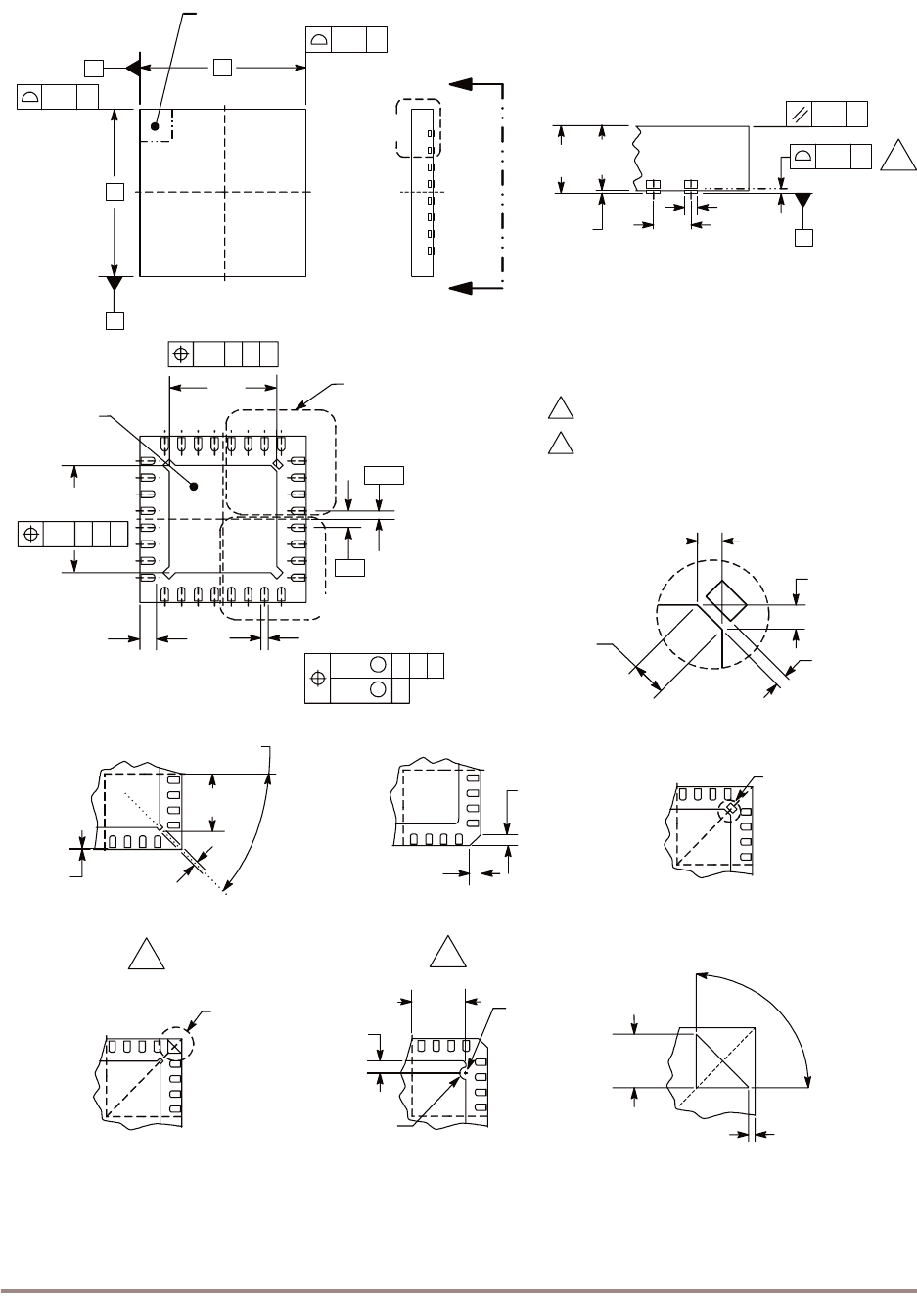
8 Packaging Information
Figure 8. Outline Dimensions for QFN-32, 5x5 mm
(Case 1311-03, Issue E)
N
EXPOSED DIE
ATTACH PAD
2.95
25
8
1
32
3.25
32X 0.18
0.30
24
17
16 9
0.5
M
0.1 C
M
0.05 C
A B
32X 0.5
0.3
C
0.1 A B
C
0.1 A B
VIEW M-M
0.25
28X
DETAIL M
PIN 1 INDEX
2.95
3.25
PIN 1
INDEX AREA
5
B
C
0.1
2X
2X
C
0.1
A5
G
M
M
1.0 1.00
0.05
C0.1
C0.05
CSEATING PLANE
5
DETAIL G
VIEW ROTATED 90° CLOCKWISE
(0.5)
(0.25)
0.8 0.75
0.00
(1.73)
(0.25)
0.065
32X 0.015
(45 )
5
4
PREFERRED CORNER CONFIGURATION
DETAIL N
0.60
0.24
0.60
0.24
4
DETAIL N
CORNER CONFIGURATION OPTION
DETAIL T
DETAIL M
BACKSIDE PIN 1 INDEX OPTION
DETAIL T
BACKSIDE PIN 1 INDEX OPTION
(90 )
5
2X
2X 0.39
0.31
0.1
0.0
DETAIL M
BACKSIDE PIN 1 INDEX OPTION
1.6
0.475
0.425
1.5 BACKSIDE
PIN 1 INDEX
0.25
0.15
R
DETAIL S
DETAIL M
PREFERRED BACKSIDE PIN 1 INDEX
0.217
0.137
(0.25)
0.217
0.137
(0.1)
DETAIL S
PREFERRED BACKSIDE PIN 1 INDEX
NOTES:
1. ALL DIMENSIONS ARE IN MILLIMETERS.
2. DIMENSIONING AND TOLERANCING PER ASME
Y14.5M, 1994.
3. THE COMPLETE JEDEC DESIGNATOR FOR THIS
PACKAGE IS: HF-PQFP-N.
4. CORNER CHAMFER MAY NOT BE PRESENT.
DIMENSIONS OF OPTIONAL FEATURES ARE FOR
REFERENCE ONLY.
5. COPLANARITY APPLIES TO LEADS, CORNER
LEADS, AND DIE ATTACH PAD.
6. FOR ANVIL SINGULATED QFN PACKAGES,
MAXIMUM DRAFT ANGLE IS 12°.
Freescale Semiconductor, I
Freescale Semiconductor, Inc.
nc...

MOTOROLA MC13192 Product Preview 19
NOTES
Freescale Semiconductor, I
Freescale Semiconductor, Inc.
nc...

MC13192/D
HOW TO REACH US:
USA/EUROPE/LOCATIONS NOT LISTED:
Motorola Literature Distribution;
P.O. Box 5405, Denver, Colorado 80217
1-303-675-2140 or 1-800-441-2447
JAPAN:
Motorola Japan Ltd.; SPS, Technical Information Center,
3-20-1, Minami-Azabu Minato-ku, Tokyo 106-8573 Japan
81-3-3440-3569
ASIA/PACIFIC:
Motorola Semiconductors H.K. Ltd.; Silicon Harbour
Centre, 2 Dai King Street, Tai Po Industrial Estate,
Tai Po, N.T., Hong Kong
852-26668334
TECHNICAL INFORMATION CENTER:
1-800-521-6274
HOME PAGE:
http://www.motorola.com/semiconductors
Information in this document is provided solely to enable system and software implementers to
use Motorola products. There are no express or implied copyright licenses granted hereunder to
design or fabricate any integrated circuits or integrated circuits based on the information in this
document.
Motorola reserves the right to make changes without further notice to any products herein.
Motorola makes no warranty, representation or guarantee regarding the suitability of its products
for any particular purpose, nor does Motorola assume any liability arising out of the application or
use of any product or circuit, and specifically disclaims any and all liability, including without
limitation consequential or incidental damages. “Typical” parameters which may be provided in
Motorola data sheets and/or specifications can and do vary in different applications and actual
performance may vary over time. All operating parameters, including “Typicals” must be validated
for each customer application by customer’s technical experts. Motorola does not convey any
license under its patent rights nor the rights of others. Motorola products are not designed,
intended, or authorized for use as components in systems intended for surgical implant into the
body, or other applications intended to support or sustain life, or for any other application in which
the failure of the Motorola product could create a situation where personal injury or death may
occur. Should Buyer purchase or use Motorola products for any such unintended or unauthorized
application, Buyer shall indemnify and hold Motorola and its officers, employees, subsidiaries,
affiliates, and distributors harmless against all claims, costs, damages, and expenses, and
reasonable attorney fees arising out of, directly or indirectly, any claim of personal injury or death
associated with such unintended or unauthorized use, even if such claim alleges that Motorola
was negligent regarding the design or manufacture of the part.
Motorola and the Stylized M Logo are registered in the U.S. Patent and Trademark Office. All other
product or service names are the property of their respective owners. Motorola, Inc. is an Equal
Opportunity/Affirmative Action Employer.
© Motorola, Inc. 2004
Freescale Semiconductor, I
Freescale Semiconductor, Inc.
nc...