0117 0257 10_K105 D_Logic_Analyzer_Addendum_68000_Disassembler_Feb84 10 K105 D Logic Analyzer Addendum 68000 Disassembler Feb84
User Manual: 0117-0257-10_K105-D_Logic_Analyzer_Addendum_68000_Disassembler_Feb84
Open the PDF directly: View PDF ![]() .
.
Page Count: 17
P-2/84
Publication
Number
0117-0257-10
Release
1.0
February 1984
Kl05-D
LOGIC
ANALYZER
USERS
MANUAL
ADDENDUM
68000
DISASSEMBLER
Gould
Inc.,
Design &
Tes~
Systems Division
4600
Old
Ironsides
Drive
Santa
Clara,
CA
95050-1279
Telephone:
(408) 988-6800
TWX/TELEX
# 910-338-0509
Copyright
© 1984.
No
part
of
this
publication
may
be
reproduced
without
written
permission
from Gou!d
!nCej
Design and
Test
Systems
Division.
Printed
in U.S.A.
f'h:::lln+o
....
....."."'"'..,.
"'.
INTRODUCTION
INTRODUCTION
•••••••
LOADING
THE
DISASSEMBLER
. . . . . . . . . .
CONTENTS
Page
• • • • • •
1-1
•••••
1-7
2
SPECIFICATIONS
PHYSICAL
DIMENSIONS
AND
WEIGHT
••••••••••••••••
2-1
3
DISPLAYS
SCREEN
DISPLAYS
OF
PREPROGRAMMED
SET
UP
MENUS
••••••••
3-1
4
INSTRUCTION
SET
Figure
1-1
1-2
3-i
3-2
3-3
3-4
3-5
68000
INSTRUCTION
SET
••••••••••••••••••••
4-1
68000 Microprocessor
Pinout
Diagram.
• • • • • • • • • • • • 1-1
Typi
ca
I
RTE
to
Target
System Connection • • • •
•••••••
1-5
Oi
sassemb;er Data Format Set
Up
Menu.
• • • • • • • • • •
••
3-1
Clock Set
Up
Menu
• • • • • • • • • • • • • • • • • • • • • • • •
3-2
Trace Contro I
Set
Up
Menu
• • • • • • • • • • • • • • • • •
3-3
Captured Data
in
Disassembled Format
•••••••••••••••
3-4
Expanded
,
nstruction.
• • • • • • • • • •
•••••••••
3-6
iif
Chap"ter 1
I
NTROOLCT
I
ON
I
NTROOOCT
ION
This
addendum
provides
the
user
with
specific
information
on
the
68000
target
microprocessor
Disassembler.
Included in
the
addendum
are
a
microprocessor
pinout
diagram,
microprocessor-to-Iogic
analyzer
connection
data,
screen
displays
of
the
preprogrammed menus, a
screen
display
of
captured
data
in
the
disassembled
format
and
special
notes
on
the
disassembler/logic
analyzer.
04
1 •
64
05
03
2
63
06
02
3
62
07
01 4
61
08
00
5
60
09
AS
6
59
010
UDS 7
58
011
-
LDS
0
57
Oi2
0
R/W
9
56
013
OTACK 10
55
014
BG
11
54
015
BGACK
12 53 GNO
BR
13
52
A23
vCC
14
51
A22
ClK
15
50
A21
GNO
16 68000 49
VCC
HALT 17
48
A20
--
RESET 18 47 A19
VMA
19
46
A18
E 20
45
A17
VPA
21
44
A16
--
BERR 22
43
A15
IPl2
23
42
A14
IPL1
24
41
A13
IPlO 25
40
A12
FC2 26 39
A11
FC1
27 38 A10
FCO
28 37 A9
A1
29
36
A8
A2
30
35
A7
A3
31
34
A6
A4
32 33
A5
0257-1-1
Figure 1-1. 68000 Microprocessor
Pinout
0 i agram
1-1
I
NTRODUCT
I
ON
Table
1-1.
Microprocessor-To-logic
Analyzer Connection Data
68000 68000 K 105-0
SIGNAL
PIN
PIN
ASSIGNMENT
04
1
A4
03
2'-
A3
02
3
A2
01
4
A1
DO
5
AO
AS
6
BJ
UOS
7
BO
lOS
8
CF
R/W
9
CE
OTACK
10
BG
11
BGACK
12
BR
13
--
..
Yvv
ClK
15
BK
GNO
16
GNO-A-B-C-O
SECT
IONS
HALT
17
RESET
18
VMA
19
E
20
VPA
21
BERR
22
IPl2
23
CO
IPl1
24
CC
IPlO
25
CB
FC2
26
CA
FC1
27
C9
FCO
28
C8
A1
29
B1
A2
30
B2
A3
31
B3
A4
32
B4
1-2
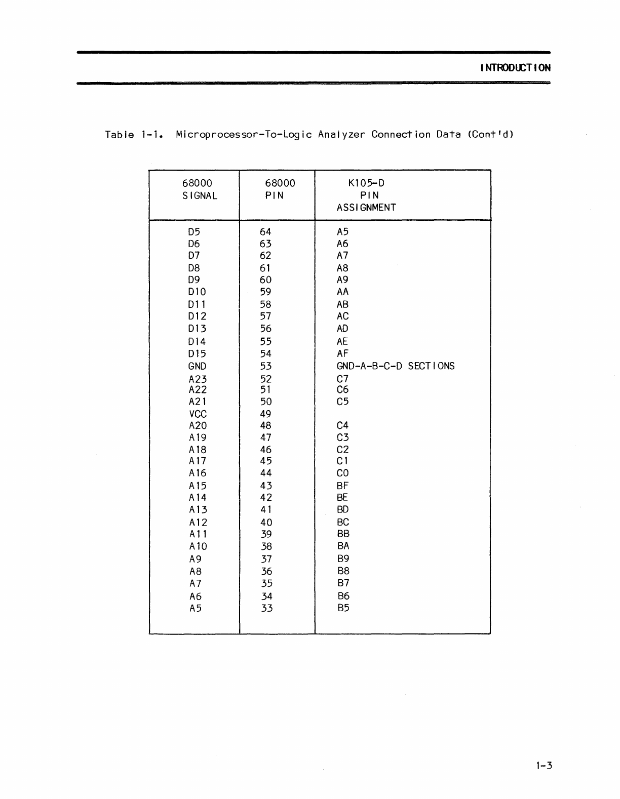
I NTfO)l£TION
Tabie
i-i.
Microprocessor-Io-Logic
Anaiyzer
Connection
Data
(Cont'd)
68000 68000 Kl05-D
SIGNAL
PIN PIN
ASSIGNMENT
D5
64
A5
D6
63
A6
D7
62
A7
D8
61
A8
D9
60
A9
Dl0
59
AA
D
11
58
AB
D12
57
AC
D13
56
AD
D14
55
AE
D15
54
AF
GND
53
GND-A-B-C-D
SECTIONS
A23
52
C7
A22
51
C6
A21
50
C5
VCC
49
A20
48
C4
A19
47
C3
A18
46
C2
A17
45
Cl
A16
44
CO
A15
43
BF
A14
42
BE
A13
41
BD
A12
40
BC
All
39
BB
Al0
38
BA
A9
37
B9
A8
36
B8
A7
35
B7
A6
34
B6
A5
33
B5
1-3
I
NTROOUCT
I
ON
ATIACl-IMENT
TO
A
TARGET
SYSTEM
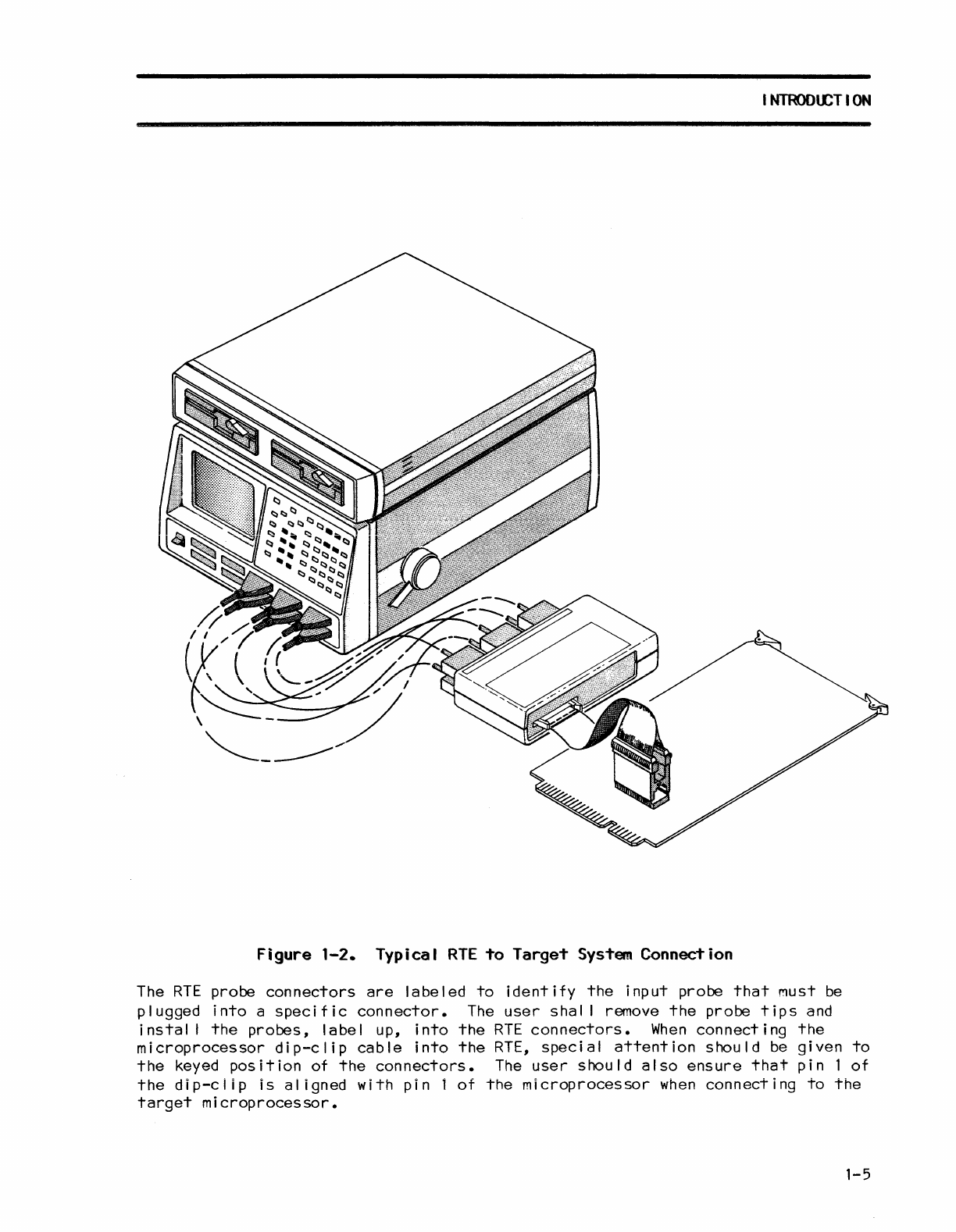
Figure
1-2
illustrates
a
typical
RTE
to
target
systeM
connection.
* * * * * * * * * * * * * * * * * * * * * * * * *
*
CAUTION
*
* *
*
In
the
event
the
microprocessor
on
your
target*
* system
is
hard-wired
to
the
board,
there
is
*
*
the
possibi
lity
of inducing
reflective
noise
*
*
into
the
test
signals.
To
eliminate
this
*
* problem,
we
recommend
varying
the
threshold
*
*
vo
I t age I
eve
I s *
* * * * * * * * * * * * * * * * * * * * * * * * *
NOTE:
Figure
1-2 shows one
of
several
possible
connections
of
the
RTE
to
a
target
system.
As
the
configuration
of
the
microprocessor
pinouts
change,
the
RTE
to
target
system
interface
may
also
change.
1-4
INTRODUCTION
Figure
1-2.
Typical
RTE
~o
Targe~
Sys~em
Connection
The
RTE
probe
connectors
are
labeled
to
identify
the
input
probe
that
Must
be
plugged
into
a
specific
connector.
The
user
shal
I remove
the
probe
tips
and
instal
I
the
probes,
label
up,
into
the
RTE
connectors.
When
connecting
the
microprocessor
dip-clip
cable
into
the
RTE,
special
attention
should
be
given
to
the
keyed
position
of
the
connectors.
The
user
should
also
ensure
that
pin
1
of
the
dip-clip
is
al igned
with
pin
1
of
The
microprocessor
when
connecting
to
the
target
microprocessor.
1-5
I
NlROOUCT
I
ON
LOAD
I
NG
THE
DISASSEMBLER
The
following procedure
provides
step-by-step
instructions
for
loading
the
Disassembler:
a.
Enter
the
Disk Operating System
screen.
b.
Gently
insert
the
disk
into
Drive
B,
with
the
disk
slot
toward
the
rear
of
the
unit
and
the
label up. Next, lock
the
disk
in
p'ace
with
the
drive
latch
handle.
c.
Depress
function
keyF3
to
display
the
B
directory.
d.
Depress 1
to
select
the
Recall
function.
e.
Use
the
right
arrow
cursor
to
enter
the
filename
field
and
then
use
either
the
up
or
down
cursor
to
seJect
the
Disassembler.
f.
Depress
function
key
F4
to
load
the
Disassembler.
g.
Depress
the
Format
key
to
enter
the'
Format
screen.
h. Depress 6
and
then
Data
to
enter
Disassemb'er
mode.
* * * * * * * * * * * * * * * * * *
*
*
*
*
*
*
*
CAUTION
*
*
*
It
is
suggested
that
the
user
*
make
a backup copy
of
the
*
master
disk
prior
to
attempting*
use
of
the
disassembler.
*
* *
* * * * * * * * * * * * * * * * * *
1-7
Chapter
2
SPEC
I
FICATIONS
PHYS
I
CAL
D I
MENS
I
ONS
AND
WE
I
GHT
Height
-
2.25
inches
(5.7
cm)
Width -
9.5
inches
(24.1
cm)
Depth -
5.5
inches
(14
cm)
Weight - 1
lb.
14
oz.
(.84
kg)
with
flat
cable
and
device
clip
ELECTRICAL
DiARACTERI
STICS
loading
(Signal
Inputs)
Input
Resistance
- 1
megohm
+2%
to
threshold
(-1.4
volts)
Input
Impedance -
150
ohms
(approximate)
Typical
Rise/Fal
I
Distortion
-heavi
Iy
dependent
on
reserve
drive
of
micro-
processor
and
its
support
devices.
The 68000
microprocessor
typically
slows
1.5
nanoseconds
on
edge
rates.
loading
(Ground/Reference Input)
Input
Resistance
-Less
than
1
ohm
referenced
to
target
system ground.
Ground
Difference
Immunity -+
0.25
volts
between
logic
analyzer
ground and
target
system ground.
Reflected
Noise
Into
Target
System
Probed with
Dip
Clip
or
Circuit
Board
Socket
-heavi
Iy
dependent
on
target
system ground.
Typically,
the
system
noise
is
reduced due
to
slower
edge
rates
caused
by
probe
load.
This
condition
occasionally
masks
the
problem being
pursued.
2-1
,
Chapter
3
DISPLAYS
SCREEN
DISPLAYS
OF
PREPROGRAMMED
SET
UP
MENUS
Figures
3-1
through
3-3
illustrate
the
preprogrammed
setup
menus downloaded
from
disk
to
the
K105-D.
Figures
3-4
and
3-5
illustrate
the
Disassembled Data
and
an
Extended
Instruction,
respectively.
When
in
the
Disassembled
Data
display,
sequential
depression
of
the
SHIFT
and V keys
causes
the
software
version
number
for
the
disassembler
to
be
displayed.
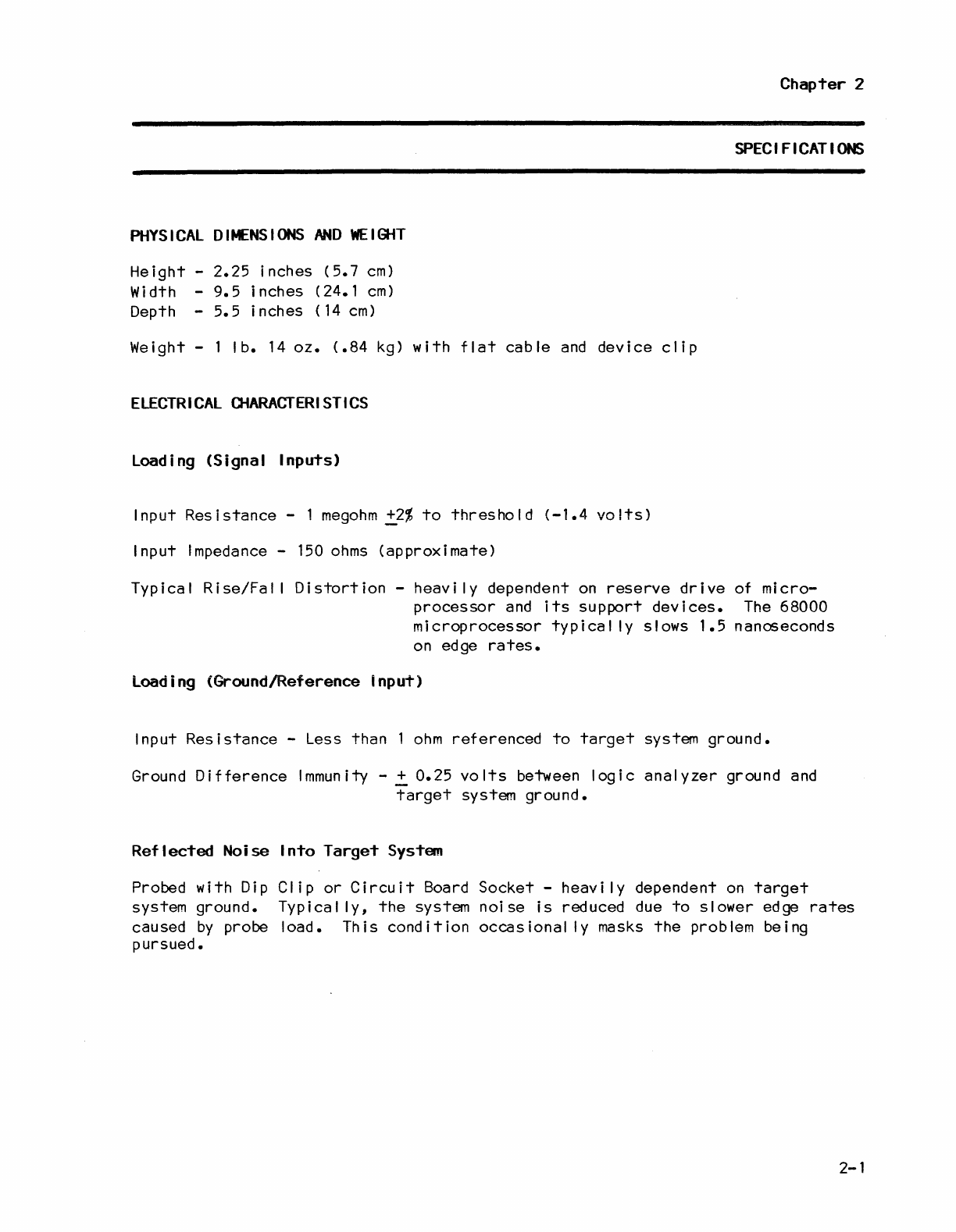
DATA
F'ORMAT
RADIX
L
SECTION
I
NPLns
DATA
INPUTS
Df'-D8
D7-D0
CF-C8
C7-C0
BF-SS
B7-·E0
AF-AS
A7-A0
CLOCK
INPUTS
SET
UP
MAIN
FORMAT
ADDR
cesses
73F'B73
62EA62
51D951
40C940
STATUS
ecce ecce
F'EDCBA99
HRESHOLD
+ 1. 4
+ 1. 4
+ 1. 4
+ L 4
+ 1. 4
+
1.
4
+ 1. 4
+ 1. 4
+
1.
4
~~DATA
FORMATI
~~TOP
THRESHOLD
MEMOR'T'=t-1
MAIN
DATA
AAAA
FB73
EA62
D951
C840
++++
++++
++++
++++
++
++
++++
++t+
++++
++++
+
+++
++++
1++++
+++,+
++,++
++++
++++
MAIN=RDY
Figure
3-1.
Disassembler Data Fonmat
Set
Up
Menu
3-1
DISPLAYS
SCREEN
DISPLAYS
OF
PREPROGRAMMED
SET
UP
MENUS
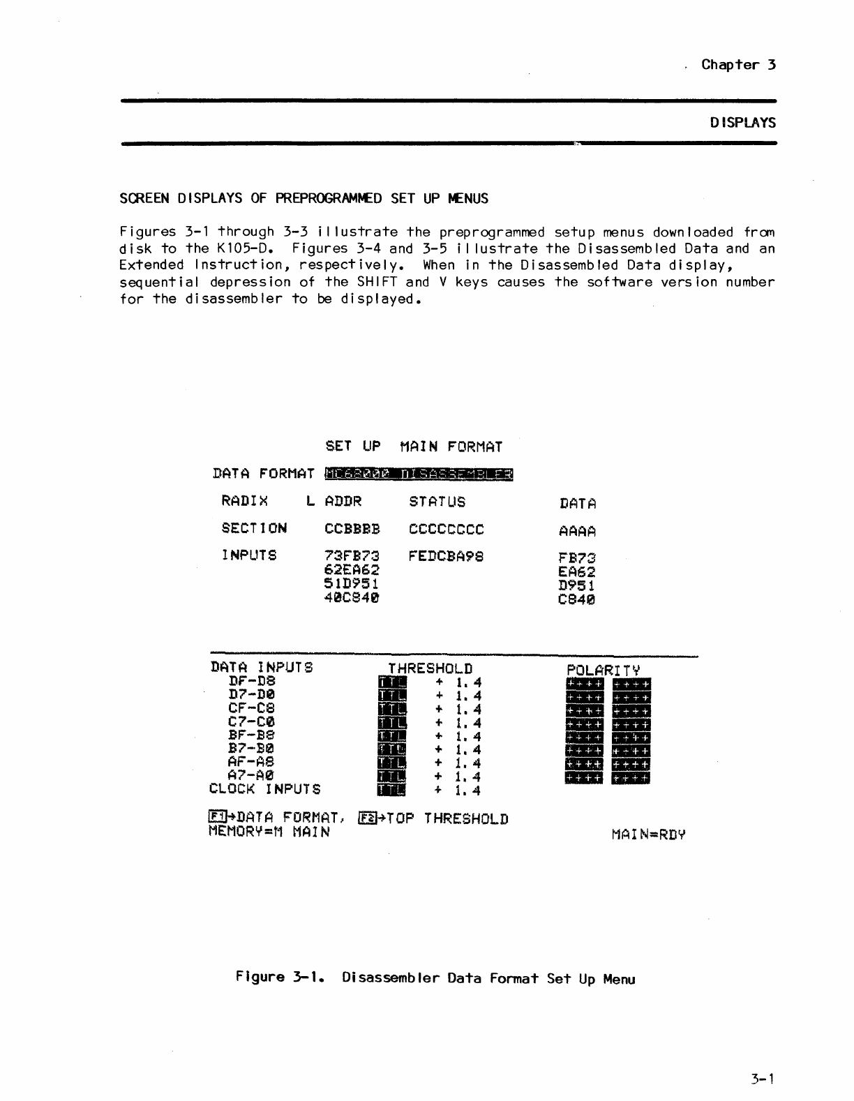
(cont'd)
SET
UP
MAIN
CLOCKS
CLOCK
SOURCE
=
MASTER
CLOCK = • L
...
SECTION
D
-,.._.
ON
lI.ldl.
SECTION
c -
SAMPLE
ON
-.1111
SECTION
B -
_ii
ON
IISliilll
SECTION
A -
SAMPLE
ON
H'
•••
EXTERNAL
CLOCK
COMBINATION
DErINITIONS
NAME: CLOCK
INPUT
S:
= <
••••
GII
••
) + (111+-'+'-'.,
= <
•••••••
) +
(~.+ID+.)
= <
•••••••
) +
(111+111+111+111)
12111··
.. 0 = (
•••••••
> +
(11+.+
....
)
HEMORY=M
MAIN
MAIN=RDY
Figure
3-2.
Clock
SeT
Up
Menu
3-2
DISPLAYS
smEEN
D I SPLAYS
OF
PREPROGRAMJED
SET
UP
tENUS
(cont'
d )
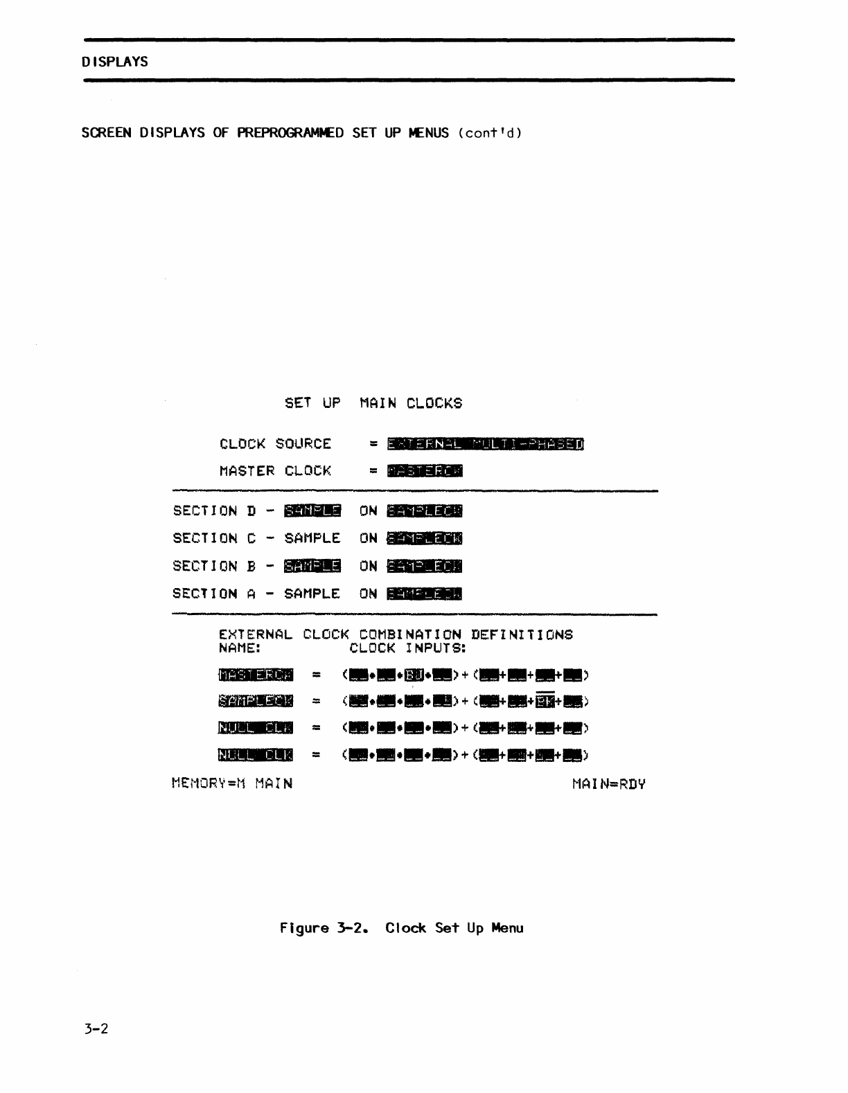
SET
UP
MAIN
TRACE
LVL
COMMAND
SEQUENCE:
0:TRACE
UNTIL
SAMPLE
=
ENABLE
l:TRACE
UNTIL
SAMPLE
=
TRIGGER
2:LINK
ON
ENTRY
TO
LEVEL
TRACE
FOR
00508
CLOCKS
PATTERN
DEFINITIONS:
NAME:
ADDR
STATUS
00
ENABLE
=XXXXXK
XXXXXXXX
01
TRIGGER
=XXXXXX
XXXXXXXX
02
_
=XXXXXX
XXXXXXXX
~TOP
CMDJ
~~TOP
PTRN
H£HORY=M
MAIN
DATA
XXXX
XXXX
XXXX
Figure
3-3.
Trace
Con~rol
Set
Up
Menu
MAIN=RDY
NOTE:
In
disassembler
mode,
the
trace
control
patterns
are
formatted
into
address,
status
and
data.
When
the
Status
field
is
selected
as
the
active
field,
the
possible
choices
are
the
status
conditions
of
the
pro-
cessor
as
fol lows:
(0
)
S-PROG-R
(8)
ACK
(1)
U-PROG-R
(
9)
INTl
( 2)
U-DATA-R
(A)
INT2
(3
)
U-DATA-W
(8)
INT3
(4)
U-PROG-W
(C)
INT4
( 5)
S-DATA-R
(D)
INT5
(6)
S-DATA-W
(E)
INT6
(7)
S-PROG-\~
(F)
INT7
In
Edit
mode,
status
bits
can
be
edited
on
a
bit-by-bit
bas i
s.
"X"
selects
al I
don't-cares.
3-3
DISPLAYS
SCREEN
DISPLAYS
OF
PRBPROGR~MED
SET
UP
MENUS
(cont'd)
3-4
MC68000
DISASSEMBLER
CLK=EXT.HLT.
S=XXXXXX
XXXX
FRAME
ADDR
OBJECT
'CODE
25 000754
S-DATA-~
26
000756
S-DATA-~
27 00007C S-DATA-R
29 08007E
S-DATA-R
29
ee991E
46FC2700
31
009922
S-PROG-R
32
009922
21CF0444
34
009926
4FFA000A
35
081444
S-DATA-~
36
080446
S-DATA-W
38
~~~~~A
£l~r~~Ub
40
ee992E
6000F35C
41
0004D6
S-DATA-~
42
0004DS
S-DATA-W
44
008C9C
4Fr90444
C
46
00SC90)4SE7FFFE
48
00SC94 4FF8178A
49
000442
S-DATA-~
5@
000440
S-DATA-~
51
000~3E
S-DATA-W
52
008430
S-DATA-W
X
MNEMONIC
L
2704
2
100e
2
000e
2
991E
2
MOVE
t$2700,SR
2
21CF
2
NOVE.L
A',$444
2
LEA
$A(PC)JA7
2
MUV~.L
BRA.L
LEA
HOVEM.L
LEA
0000
2
0754
2
~/J~4Ub
~
$F35C(PC) 2
000e
2
9932
2
$444~A7
2
D0/DI/D2/D3/D4/D
2
$78A~A7
2
0540
2
0000 2
0540
2
0080
2
CONTROL=0846
REF=1023
R-C=+
977
~~PG
UP
~PG
DOWN
~~DSPLY
DBJ
~DSPLY
MNEMONICS
MEMORY=A
MAIN
MAIN=RDY
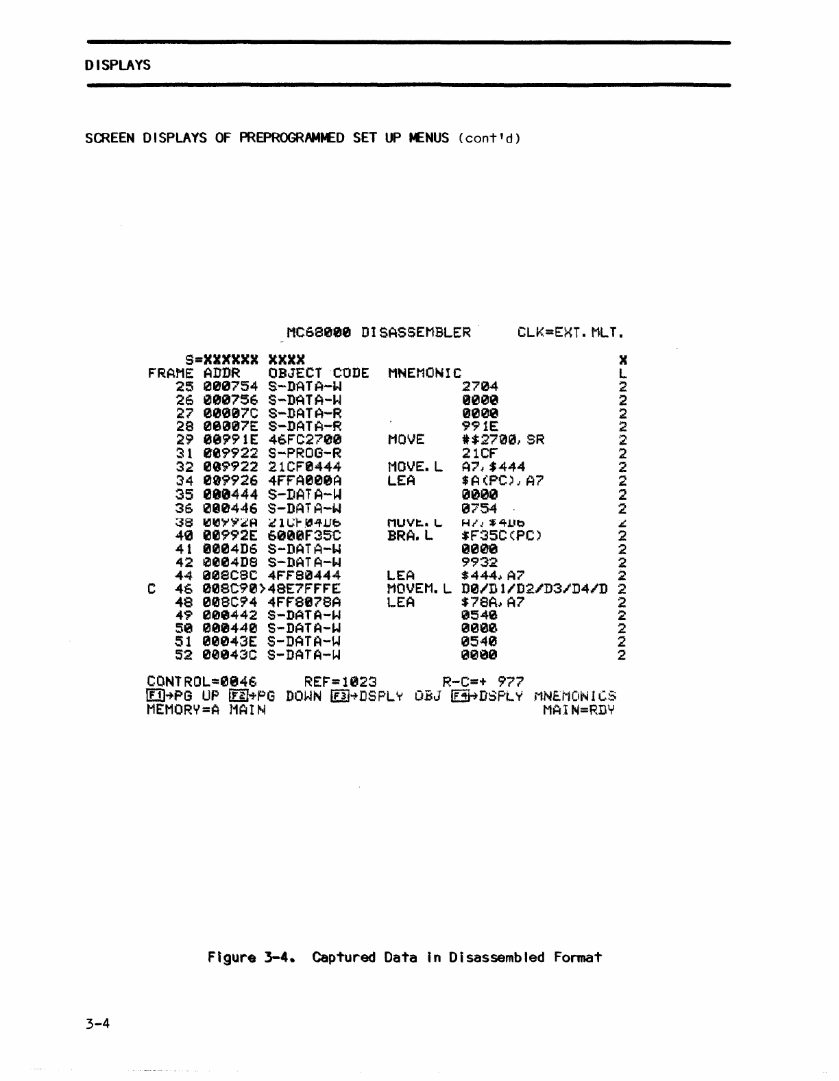
Figure
3-4.
Captured Data
In
Disassembled
Fonmat
DISPLAYS
NOTES:
1.
After
the
disassembler
data
format,
and
clock
select
menus
of
the
logic
analyzer
are
pre-programmed,
the
trace
control
selections
must
be
made
by
the
user
before
making a
recording.
The
trace
control
selections
determines
exactly
which
portions
of
the
data
stream
are
recorded
or
ignored.
2.
The
object
code
or
operand
of
an
instruct
ion
may
be
too
long in
some
cases
to
be
displayed
on
the
K105-D
screen.
In
these
cases,
a
greater
than
symbol
(»
is
used
to
mark
the
code
that
has been
truncated.
The
user
can
move
the
cursor
to
the
indicated
frame,
depress
the
SHIFT
key
and
then
the
E
key
to
obtain
an
instruction
expansion
on
the
screen
(see
Figure
3-5).
3.
When
monitoring
the
68000
pinout,
words
with
"Program Read"
status
are
being
fetched
to
be
put
into
the
queue.
Not
al I
instruction
words
fetched
are
executed",
Instruction
words not executed
are
displayed
with
the
"Program
Read"
status.
Refer
to
the
~68000
Users
Manua
I.
4.
The
SEARCH
and
COMPARE
keys
are
not
active
in
the
Data
Display
Screen.
The
Edit
mode
can be used
to
change
the
search
word.
After
leaving
Edit
mode,
the
NEXT
and
PREVIOUS
keys
locate
target
data
in
memory.
If
the
search
word
is
not
active,
the
NEXT
and
PREVIOUS
keys
update
the
display
to
the
next
or
previous
trace
level
transition.
5.
Depression
of
the
F3
function
key
changes
the
display
of
recorded
infor-
mation.
Code
is
not
disassembled,
but
recorded
information
is
displayed
from
the
control
cursor
(C)
position
to
the
end
of
memory
as
frame number,
address,
status
and
data.
If
recorded
data
is
displayed
in
object
format,
depressing
the
F4
function
key
invokes
the
disassembly
process
for
data
from
the
control
cursor
to
the
end
of
memory.
6.
II
legal
instructions
are
displayed
as
111.
7.
A
Move
to
SR
or
CCR
causes
an
extra
clock
cycle
and
duplication
of
the
address
and
data.
See
Figure
3-4,
frames
31
and
32.
8.
The
disassembler
is
first
downloaded
from
disk
to
the
K105-D
and
the
disassembler
format
is
selected.
Then
the
trace
patterns
are
configured
,as
desired.
It
is
suggested
that
the
user
make
a backup copy of
the
master
disk
prior
to
attempting
use of
the
disassembler.
3-5
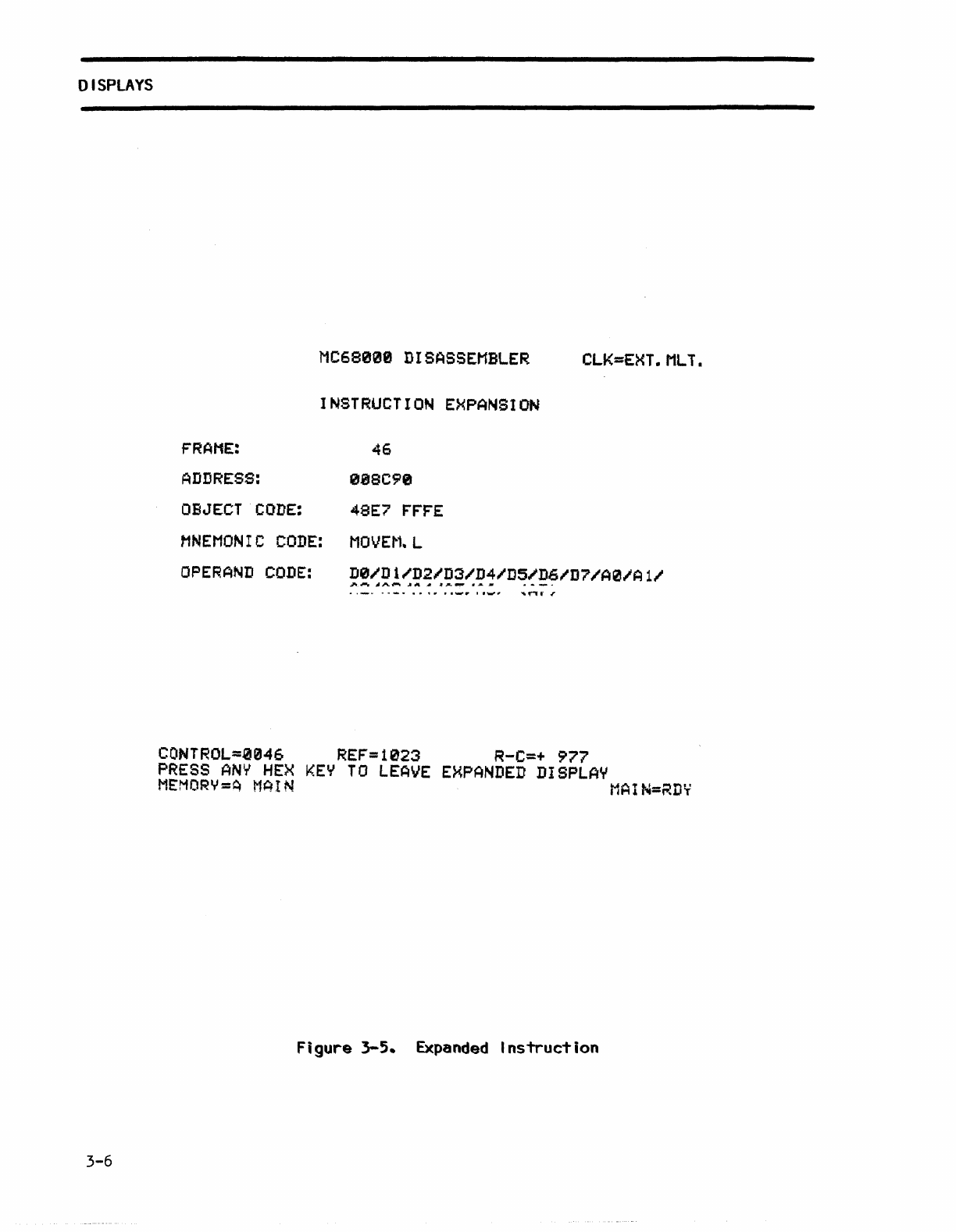
DISPLAYS
NC68008
DISASSEMBLER
CLK=EXT.
ML
T •
INSTRUCTION
EXPANSION
FRANE:
46
ADDRESS:
008C90
DEJECT
CODE:
48E7 rFFE
MNEMONIC
CODE:
MOVEM.L
OPERAND
CODE:
D0/Dl;D2/D3/D4/D5~D6/D7/A0/A1/
•.
-~
....
_-
••••
,
.'-"P
••
...,.....
....."..r
CONTROL=0046
REF=1023
R-C=+
977
PRESS
ANY
HEX
KEY
TO
LEAVE
EXPANDED
DISPLAY
MEHORY=A
MAIN
MAIN=RDY
Figure
3-5.
Expanded
Instruction
3-6
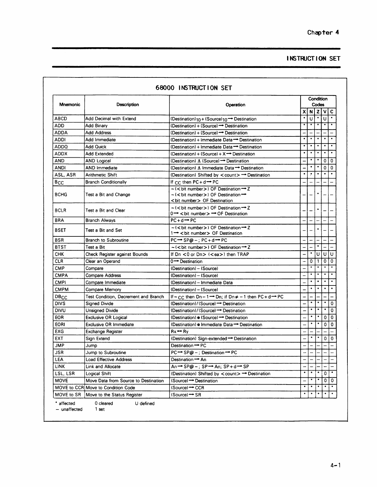
Mnemonic
ABCD
ADD
ADDA
ADDI
ADDQ
ADDX
AND
ANDI
ASL.ASR
BCC
BCHG
BClR
BRA
BSET
BSR
BTST
CHK
CLR
CMP
CMPA
CMPI
CMPM
DBCC
DIVS
DIVU
EOR
EORI
EXG
EXT
JMP
JSR
LEA
LINK
LSL.
LSR
MOVE
MOVE
to
CCR
MOVE to
SR
• affected
-unaffected
68000 I
NSTRUCT
I
ON
SET
Description
Add Decimal
with
Extend
Add Binary
Add Address
Add Immediate
Add Quick
Add Extended
AND Logical
AND Immediate
Arithmetic Shift
Branch Conditionally
Test a Bit and Change
I Test a Bit and Clear
Branch Always
T est a Bit and Set
Branch
to
Subroutine
Test a Bit
Check Register against Bounds
Clear
an
Operand
Compare
Compare Address
Compare Immediate
Compare Memory
Test Condition. Decrement and Branch
Signed Divide
Unsigned Divide
Exclusive
OR
Logical
Exclusive
OR
Immediate
Exchange Register
Sign Extend
Jump
Jump to Subroutine
Load Effective Address
Link and Allocate
Logical Shift
Move Data from Source to Destination
Move to Condition Code
Move to the Status Register
o cleared
1
set
U defined
Operation
(Destination)
10
+
(Source)1O-
Destination
(Destination) + (Source) -Destination
(Destination) + (Source) -Destination
(Destination) + Immediate
Data-
Destination
(Destination) + Immediate
Data-
Destination
(Destination) + (Source) + X - Destination
!Destination) A (Source) -Destination
!Destination) A Immediate Data -Destination
(Destination) Shifted by
<count>
-Destination
If
CC
then
PC+d-
PC
- « bit
number»
OF
Destination-Z
- « bit
number»
OF
Destination-
< bit
number>
OF
Destination
1-
« bit
number»
OF
Destination - Z
0-
<bit
number>
-OF
Destination
PC+d-PC
-«bit
number»
OF
Destination-Z
1-
< bit
number>
OF
Destination
PC-SP@-;
PC+d-PC
-«bit
number»
OF
Destination-Z
If
On
<Oor
On>
«ea»
then TRAP
0-
Destination
(Destinationi -(Source)
(Destination) -(Source)
(Destination) -Immediate Data
(Destination) -(Source)
If-
CC
then
Dn-1-
On;
if
Dn*
-1
then
PC+
d-
PC
(Destination) I (Source) -Destination
(Destination)1 (Source) -Destination
!Destination).
(Source) -Destination
(Destination) • Immediate
Data-
Destination
Rx-Ry
(Destination)
Sign-extended-
Destination
Destination -
PC
PC-
SP@-;
Destination-
PC
Destination -An
An-SP@-;
SP-An;
SP+d-SP
(Destination) Shifted by
<count>
-Destination
(Source) -Destination
(Sourcel-
CCR
(Source)-
SR
Chapter
4
I
NSTRJCT
I
ON
SET
Condition
Codes
X N Z V C
..
U
..
U
..
..
..
..
.. ..
-- - - -
..
.. ..
..
..
.. ..
..
.. ..
..
..
· · .
-· · 0 0
-· · 0 0
..
.-
.- .-
..
--- - -
·
- - - -
·
- - - -
--- - -
·
--- -
---- -
·
-- - -
-· U U U
-0 1 0 0
" " " "
-· · · .
-
..
·
..
..
-
..
..
..
..
-
- - ---
-
..
· · 0
-
..
.. ..
0
-
..
..
0 0
-·
..
0 0
--- - -
-·
..
0 0
-----
-----
-----
--- - -
. ·
..
0
..
-
..
· 0 0
.. ..
· ·
..
..
..
·
..
..
4-1
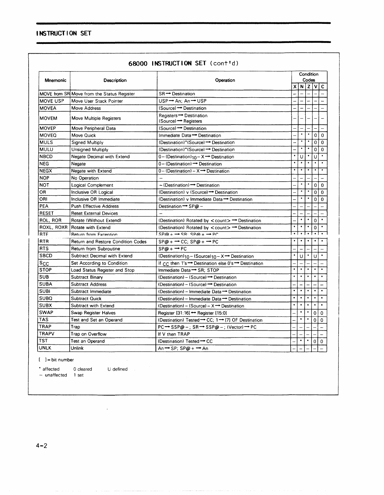
I
NSTRUCT
I
ON
SET
68000
I
NSTRUCT
I
ON
SET
(cant'
d )
Condition
Mnemonic Description Operation
Codes
X N Z V C
MOVE
from
SR
Move from the Status Register
SR
-Destination --- - -
MOVE USP Move
User
Stack Pointer
USP-
An;
An-
USP
--- - -
MOVEA Move Address (Source) -Destination -----
MOVEM Move Multiple Registers
Registers-
Destination -----
(Source) -Registers
MOVEP Move Peripheral Data (Source) -Destination - - ---
MOVEQ Move Quick Immediate Data -Destination -· · 0 0
MULS Signed Multiply (Destination)' (Source) -Destination -· · 0 0
MULU Unsigned Multiply (Destination)'(Source) -Destination -· · 0 0
NBCD Negate Decimal with Extend
0-\Destination)1O-
X - Destination · U · U ·
NEG
Negate
0-
(Destination) -Destination · · · · ·
NEGX
Negate with Extend
0-
(Destination) -
X-
Destination · · · · ·
NOP
No
Operation ---- - -
NOT Logical Complement -\Destination) -Destination -· · 0 0
OR
Inclusive
OR
Logical (Destination) v (Source) -Destination -· · 0 0
ORI
Inclusive
OR
Immediate \Destination) v Immediate Data -Destination -· · 0 0
PEA
Push
Effective Address
Destination-
SP@-
---- -
RESET
Reset
External Devices ----- -
ROL,
ROR
Rotate (Without Extend) \Destination) Rotated by <
count>
-Destination -· · 0 ·
ROXL,
ROXR
Rotate with Extend \Destination) Rotated by <
count>
-Destination · · · 0 ·
RTE
Rp.tl.lrn
from
FxrAotjnn
SPrn>
-I- -
C::R·
C::Pi/V
-I- -
pr
· · · · ·
--
RTR
Return and Restore Condition Codes SP@+
-CC;
SP@+-PC
· · · · ·
RTS
Return from Subroutine SP@+ -
PC
-----
SaCD Subtract Decimal with Extend \Destination)
10-
(Source)1O- X - Destination · U · U ·
SCC
Set According to Condition If
CC
then
1's-
Destination
else
O's-
Destination - - - - -
STOP
Load
Status Register and Stop Immediate
Data-
SR;
STOP
· · · · ·
SUB Subtract Binary \Destination) -(Source) -Destination · · · · ·
SUBA Subtract Address \Destination) -(Source) -Destination - - - - -
SUBI Subtract Immediate \Destination) -Immediate Data -Destination · · · · ·
SUBQ Subtract Quick \Destination)
-Immediate
Data-
Destination · · · · ·
SUBX Subtract with Extend (Destination) -(Source) -
X-
Destination · · · · ·
SWAP Swap Register Halves Register
[31:16]-
Register [15:0] -· · 0 0
TAS Test and Set
an
Operand \Destination)
Tested-
CC;
1-
[7]
OF
Destination -· · 0 0
TRAP Trap
PC-SSP@-;
SR-SSP@-;
(Vector)-PC
- - ---
TRAPV Trap
on
Overflow If V then TRAP - - ---
TST Test
an
Operand \Destination) Tested -
CC
-· · 0 0
UNLK Unlink
An-SP;
SP@+
-An
- - - --
[ ] = bit number
• affected o cleared U defined
-unaffected 1
set
4-2
