03 0027 02_Z80_CPU_Product_Specification_Mar78 02 Z80 CPU Product Specification Mar78
User Manual: 03-0027-02_Z80_CPU_Product_Specification_Mar78
Open the PDF directly: View PDF ![]() .
.
Page Count: 10
Z80':CPU
Z80A-CPU
The Zilog Z80 product line
is
a complete set
of
micro-
computer components, development systems and support
software. The Z80 microcomputer component set includes
all
of
the circuits necessary to build high-performance
microcomputer systems ,with virtually no other logic and a
minimum number
of
low cost standard memory elements.
The Z80 and Z80A CPU's are third generation single chip
microprocessors with unrivaled computational power. This
increased computational power results in higher system
through-put and more efficient memory utilization when
compared
to
second generation microprocessors. In
addition, the Z80 and Z80A CPU's are very easy to imple-
ment into a system because
of
their
single voltage require-
ment plus all output signals are fully decoded and timed to
control standard memory or peripheral circuits_ The circuit
is
implemented using
an
N-channel, ion implanted, silicon
gate
MaS
process.
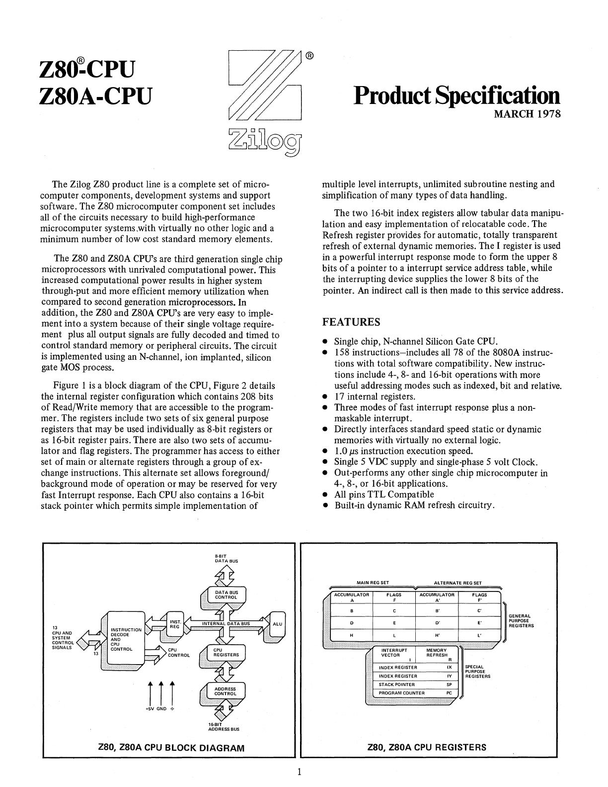
Figure 1
is
a block diagram
of
the CPU, Figure 2 details
the internal register configuration which contains 208 bits
of
Read/Write memory that are accessible to the program-
mer. The registers include two sets
of
six general purpose
registers that may be used individually
as
8-bit registers or
as
16-bit register pairs. There are also two sets
of
accumu-
lator and
flag
registers. The programmer has access to either
set
of
main or alternate registers through a group
of
ex-
change instructions. This alternate set allows foreground/
background mode
of
operation
or
may
be
reserved for very
fast Interrupt response. Each
CPU
also contains a 16-bit
stack pointer which permits simple implementation
of
13
CPU
AND
SYSTEM
~:;'~}:L~L
\:"~Hi%:1
r r r
+5V GNO 'I'
a-BIT
DATA
BUS
16-81T
ADDRESS
BUS
Z80,
Z80A
CPU
BLOCK
DIAGRAM
1
Product
Specification
MARCH 1978
multiple
level
interrupts, unlimited subroutine nesting and
simplification
of
many types
of
data handling.
The two 16-bit index registers allow tabular data manipu-
lation and easy implementation
of
relocatable code. The
Refresh register provides for automatic, totally transpare'nt
refresh
of
external dynamic memories. The I register
is
used
in a powerful interrupt response mode to form the upper 8
bits
of
a pointer to a interrupt service address table, while
the interrupting device supplies the lower 8 bits
of
the
pointer.
An
indirect call
is
then made to this service address.
FEATURES
• Single chip, N-channel Silicon Gate
CPU.
• 158 instructions-includes
all
78'
of
the 8080A instruc-
tions with total software compatibility. New instruc-
tions include 4-, 8- and 16-bit operations with more
useful addressing modes such
as
indexed, bit and relative.
•
17
internal registers.
• Three modes
of
fast interrupt response plus a non-
maskable interrupt.
• Directly interfaces standard speed static or dynamic
memories with virtually no external logic.
• 1.0 /ls instruction execution speed.
• Single 5
VDC
supply and single-phase 5 volt Clock.
• Out-performs any other single chip microcomputer
in
4-, 8-, or 16-bit applications.
•
All
pins TTL Compatible
• Built-in dynamic
RAM
refresh circuitry.
MAIN
REG
SET
ALTERNATE
REG
SfT
, v
ACCUMULATOR
fLAGS
ACCUMULATOR
FLAGS
A F
A'
F'
B C B'
C'
D E
D'
E'
H L
H'
L'
!i!:;!!'!'{i;;g;'T;;;HTH;;';;H;
:L!!ii;ijI'
INTERRUPT MEMORY
VECTOR REFRESH
I R
INDEX
REGISTER
IX
SPECIAL
PURPOSE
INDEX
REGISTER
IV
REGISTERS
STACK POINTER
SP
PROGRAM COUNTER
PC
iHi1f.iiiiU3i,;;;;V
Z80,
Z80A
CPU
REGISTERS
"
]
GENERAL
PURPOSE
REGISTERS
Z80, Z80A-CPU Pin Description
MREQ
SYSTEM !.::RQ
{
Ml
CONTROL
RD
ViR
RFSH
WAIT
CPU
{
HALT
CONTROL
~
NM'
RESET
CPU
{BUSAa
BUS
CONTROL BUSAK
'SV
GND
19
20
"
ZBO-CPU
Z80A·CPU
"0
A,
A,
A3
A,
AS
A,
A7
ADDRESS
AS BUS
A,
AIO
A"
A"
A"
A14
A"
Z80, Z80A
CPU
PIN CONFIGURATION
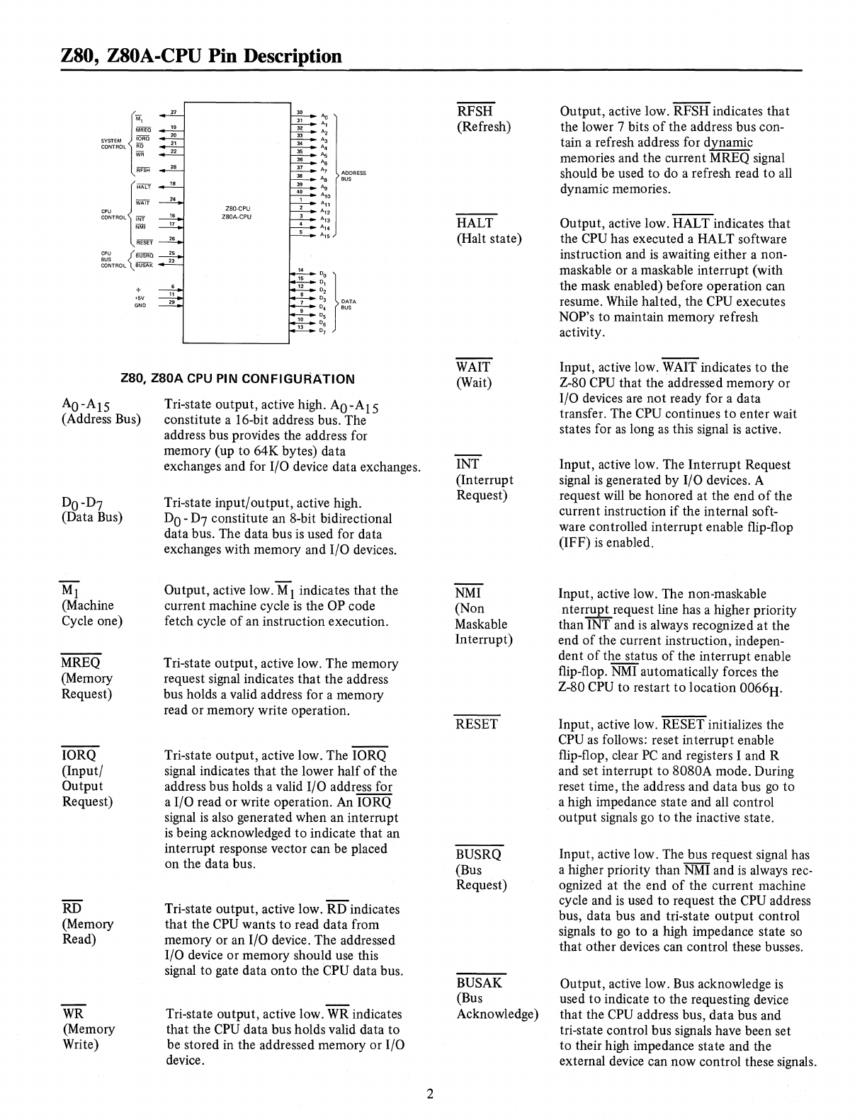
AO-A15
(Address Bus)
DO-D7
(Data Bus)
Ml
(Machine
Cycle one)
MREQ
(Memory
Request)
10RQ
(Input/
Output
Request)
RD
(Memory
Read)
WR
(Memory
Write)
Tri-state output, active high. AO-A15
constitute a 16-bit address bus. The
address bus provides the address for
memory (up to 64K bytes) data
exchanges and for I/O device data exchanges.
Tri-state input/output, active high.
DO
-
D7
constitute an 8-bit bidirectional
data bus. The data bus
is
used for data
exchanges with memory and I/O devices.
Output, active low. M 1 indicates that the
current machine cycle
is
the
OP
code
fetch cycle
of
an instruction execution.
Tri-state output, active low. The memory
request signal indicates that the address
bus holds a valid address for a memory
read or memory write operation.
Tri-state output, active low. The 10RQ
signal indicates that the lower half
of
the
address bus holds a valid I/O address for
a I/O read or write operation.
An
10RQ
signal
is
also generated when an interrupt
is
being acknowledged
to
indicate that an
interrupt response vector
canbe
placed
on the data bus.
Tri-state output, active low. RD indicates
that the
CPU
wants to read data from
memory or an I/O device. The addressed
I/O device or memory should
use
this
signal to gate data onto the CPU data bus.
Tri-state output, active low.
WR
indicates
that the
CPU
data bus holds valid data to
be stored
in
the addressed memory or I/O
device.
2
RFSH
(Refresh)
HALT
(Halt state)
WAIT
(Wait)
INT
(Interrupt
Request)
NMI
(Non
Maskable
Interrupt)
RESET
BUSRQ
(Bus
Request)
BUSAK
(Bus
Acknowledge)
Output, active low. RFSH indicates that
the lower 7 bits
of
the address bus con-
tain a refresh address for dynamic
memories and the current MREQ signal
should be used to
do
a refresh read to
all
dynamic memories.
Output, active low. HALT indicates that
the
CPU
has executed a HALT software
instruction and
is
awaiting either a non-
mask able or a maskable interrupt (with
the mask enabled) before operation can
resume.
While
halted, the
CPU
executes
NOP's to maintain memory refresh
activity.
Input, active low.
WAIT
indicates to the
Z-80
CPU
that the addressed memory or
I/O devices
are
not ready for a data
transfer. The CPU continues
to
enter wait
states for
as
long
as
this signal
is
active.
Input, active low. The Interrupt Request
signal
is
generated by I/O devices. A
request
will
be
honored at the end
of
the
current instruction
if
the internal soft-
ware controlled interrupt enable flip-flop
(IFF)
is
enabled.
Input, active low. The non-maskable
nterrupt request line has a higher priority
than INT and
is
always recognized at the
end
of
the current instruction, indepen-
dent
of
the status
of
the interrupt enable
flip-flop.
NMI
automatically forces the
Z-80
CPU
to restart
to
location 0066H'
Input, active low. RESET initializes the
CPU
as
follows: reset interrupt enable
flip-flop, clear
PC
and registers I and R
and set interrupt to 8080A mode. During
reset time, the address and data bus
go
to
a high impedance state and
all
control
output signals
go
to the inactive state.
Input, active low. The bus request signal has
a higher priority than
NMI
and
is
always rec-
ognized at the end
of
the current machine
cycle and
is
used to request the
CPU
address
bus, data bus and tri-state output control
signals to
go
to a high impedance state
so
that other devices can control these busses.
Output, active low.
Bus
acknowledge
is
used to indicate
to
the requesting device
that the
CPU
address bus, data bus and
tri-state control bus signals have been set
to their high impedance state and the
external device can now control these signals.
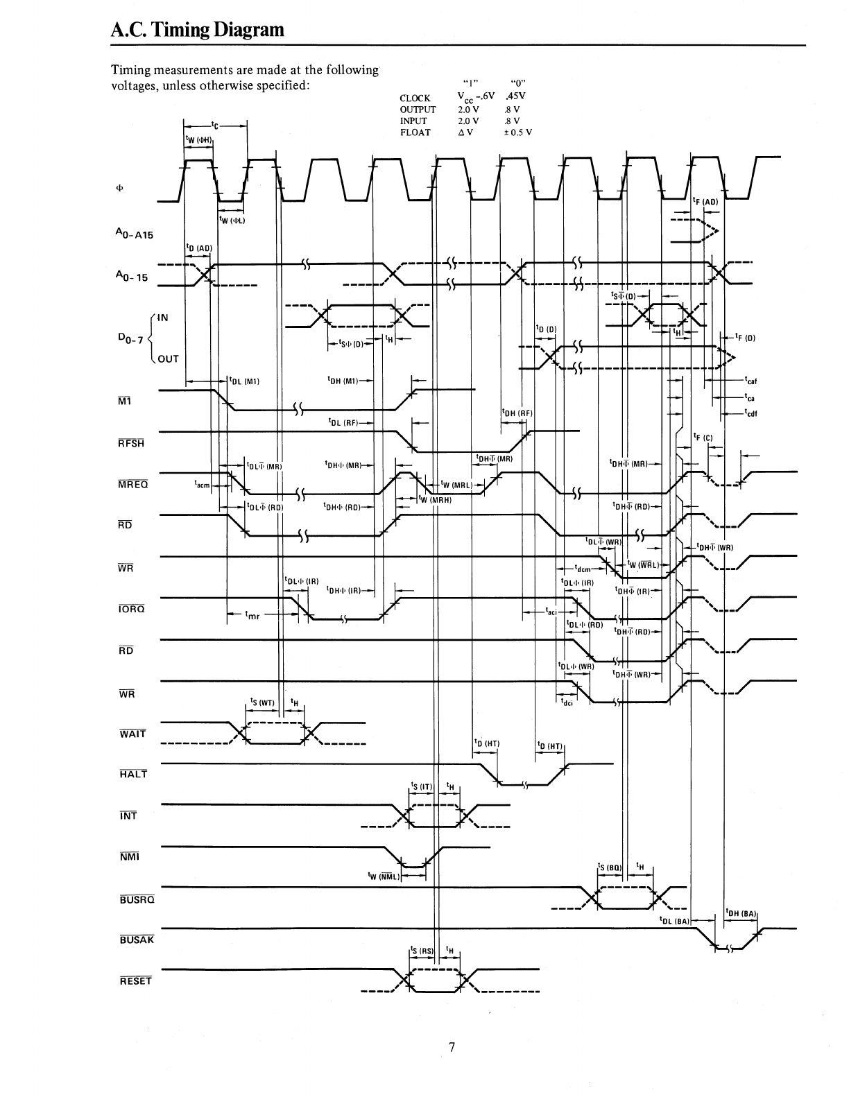
Timing
Waveforms
INSTRUCTION
OP
CODE FETCH
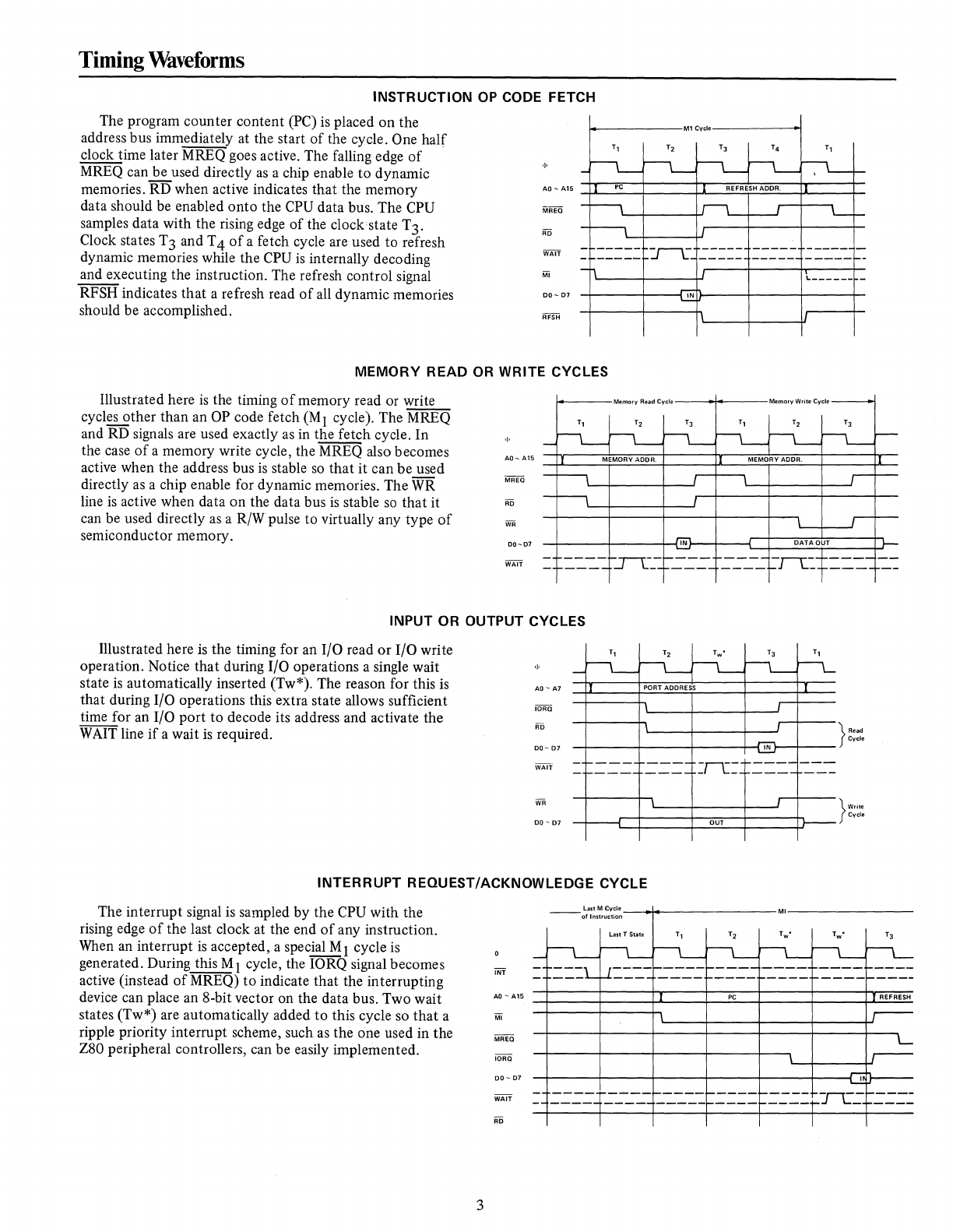
The program counter content (PC)
is
placed
on
the
address bus immediately at the start
of
the cycle. One half
clock time later MREQ goes active. The falling edge
of
.
MREQ
can be used directly
as
a chip enable
to
dynamic
memories. RD when active indicates that the memory
data should be enabled onto the
CPU
data bus. The CPU
samples data with the rising edge
of
the clock state T3.
Clock states T 3 and T 4
of
a fetch cycle are used to refresh
dynamic memories while the
CPU
is
internally decoding
and executing the instruction. The refresh control signal
RFSH indicates that a refresh read
of
all dynamic memories
should be accomplished.
-,-
AD""
A15
4JL-':":'---+---l-A-~==r-:="---!A---+-
L
______
_
co-
01
IN
MEMORY
READ OR WRITE CYCLES
Illustrated here
is
the timing
of
memory read or write
cycl~ther
than an
OP
code fetch
(M
1 cycle). The MREQ
and RD signals are used exactly
as
in
the fetch cycle. In
the case
of
a memory write cycle, the MREQ also becomes
active when the address bus
is
stable
so
that it can be used
directly
as
a chip enable for dynamic memories. The
WR
line
is
active when data on the data bus
is
stable
so
that it
can be used directly
as
a R/W pulse to virtually any type
of
semiconductor memory.
-,-
AD
....
A15
00-07
WAIT
-
-=-
____
-
:IL-_-
IN
DATA
OUT
INPUT OR OUTPUT CYCLES
Illustrated here
is
the timing for an I/O read
or
I/O write
operation. Notice that during I/O operations a single wait
state
is
automatically inserted (Tw*). The reason for this
is
that during I/O operations this extra state allows sufficient
time for an I/O port to decode its address and activate the
WAIT
line
if
a wait
is
required.
-,.
AD
....
A7
00-0,'
00""
07
-~~~
PORT ADDRESS
...!!:!..,
-1----
---
:,---c:
----
-
---
----
----
OUT
~
}
...
d
Cvcle
---
---
~
INTERRUPT REQUEST/ACKNOWLEDGE CYCLE
The interrupt signal is sampled by the
CPU
with the
rising edge
of
the last clock at the end
of
any instruction.
When
an interrupt
is
accepted, a special M 1 cycle
is
generated. During this M 1 cycle, the IORQ signal becomes
active (instead
of
MREQ)
to
indicate that the interrupting
device can place an 8-bit vector on the data bus. Two wait
states (Tw*) are automatically added
to
this cycle so
that
a
ripple priority interrupt scheme, such as the one used in the
Z80 peripheral controllers, can be easily implemented.
3
Last
M
Cycle_--I-o__------M'--------
--of
Instruction
AO""
A15
~===t:==:t:x==::t:::::JPC~:::t===~==~E
'.E~F.~EESH
lORD
00-
07
,....,-1}..--
-.....;;
WAIT -
----
----r----r----~----
-,,--r----
_
-----
----
_____
1-
____
1-____
J
L_
--
__
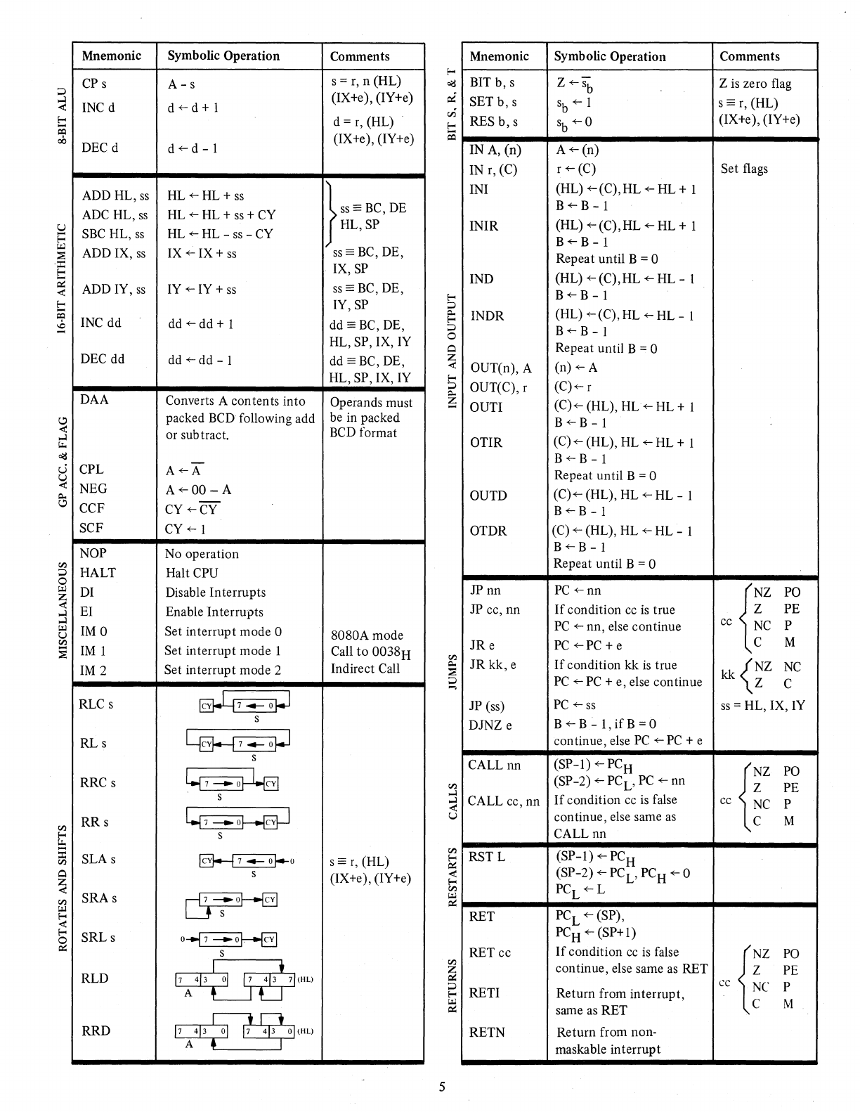
Z80, Z80A Instruction Set
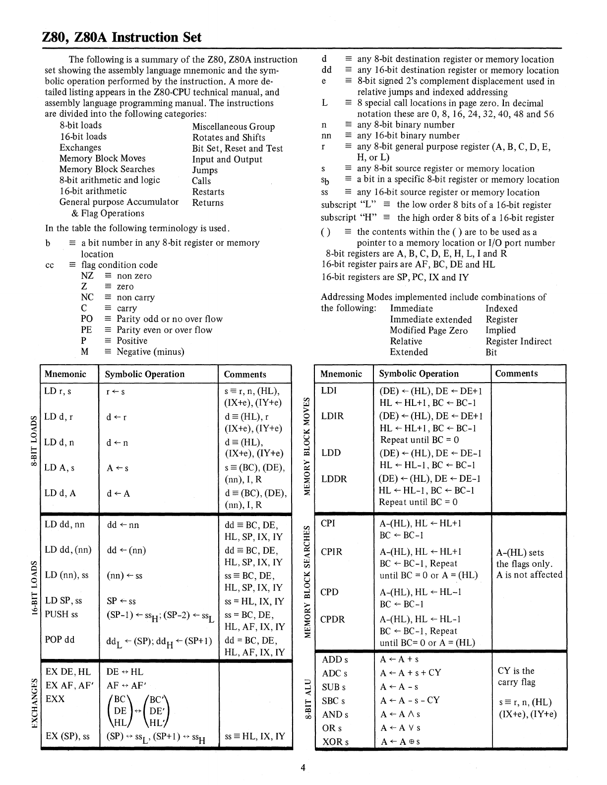
The following
is
a summary
of
the Z80, Z80A instruction
set showing the assembly language mnemonic and the sym-
bolic operation performed
by
the instruction. A more de-
tailed listing appears in the Z80-CPU technical manual, and
assembly language programming manual. The instructions
are divided into the following categories:
8-bit loads
16-bit loads Miscellaneous Group
Rotates and Shifts
Exchanges
Memory Block Moves
Memory Block Searches
8-bit arithmetic and logic
16-bit arithmetic
Bit Set, Reset and Test
Input and
Output
Jumps
Calls
Restarts
General purpose Accumulator Returns
& Flag Operations
In the table the following tenninology
is
used.
b a
bit
number in any 8-bit register or memory
location
cc
flag
condition code
NZ
non zero
Z zero
NC
non carry
C carry
PO
Parity
odd
or
no
over flow
PE Parity even
or
over flow
P Positive
M Negative (minus)
Mnemonic Symbolic Operation Comments
LD
r,
s r
+-
s s
==
r,
n, (HL),
(IX+e) , (IY+e)
LD
d, r
d+-r
d==(HL),r
(IX+e) , (IY+e)
LDd,n
d+-n
d
==
(HL),
(IX +e), (IY +e)
LDA,s
A+- s s
==
(BC), (DE),
(nn), I, R
LDd,A
d+-A
d
==
(BC), (DE),
(nn), I, R
LD
dd, nn dd
+-
nn
dd
==
BC,
DE,
HL, SP, IX,
IY
LD
dd, (nn) dd
+-
(nn) dd
==
BC,
DE,
HL, SP, IX, IY
LD
(nn),
ss
(nn)
+-
ss
ss==
BC,
DE,
HL, SP, IX, IY
LD
SP,
ss
SP
+-
ss
SS
= HL, IX,
IY
PUSH
ss
(SP-l)
+-
sSH;
(SP-2)
+-
sSL
ss
=
BC,
DE,
HL, AF, IX,
IY
POPdd
ddL
+-
(SP); ddH
+-
(SP+l) dd =
BC,
DE,
HL, AF, IX,
IY
EX
DE,HL
DE
<+
HL
EX
AF,AF'
AF
<+
AF'
EXX
(BC)
(BC)
DE
<+
DE'
HL HL'
EX
(SP),
ss
(SP) H
ssu
(SP+
I)
B
sSH
ss
==
HL, IX,
IY
4
d -any 8-bit destination register
or
memory location
dd any 16-bit destination register or memory location
e 8-bit signed 2's complement displacement used in
relative jumps and indexed addressing
L 8 special call locations in page zero. In decimal
notation these are 0, 8, 16,
24,32,40,
48 and
56
n -any 8-bit binary number
nn
any 16-bit binary number
r any 8-bit general purpose register (A, B, C, D, E,
H, or L)
s -any 8-bit source register or memory location
sb
a
bit
in a specific 8-bit register or memory location
ss
any 16-bit source register
or
memory location
subscript
"L"
==
the low order 8 bits
of
a 16-bit register
subscript
"H"
==
the high order 8 bits
of
a 16-bit register
( )
==
the contents within the ( ) are to be used
as
a
pointer
to
a memory location or I/O
port
number
8-bit registers are A,
B,
C,
D,
E,
H,
L,
I and R
16-bit register pairs are AF,
BC,
DE and HL
16-bit registers are SP, PC, IX and IY
Addressing Modes implemented include combinations
of
the following: Immediate Indexed
Immediate extended Register
Modified Page Zero Implied
Relative Register Indirect
Extended Bit
Mnemonic Symbolic Operation Comments
LDI (DE)
+-
(HL), DE
+-
DE+l
HL
+-
HL+l,
BC
+-
BC-l
LDIR (DE) +- (HL), DE
+-
DE+ 1
HL
+-
HL+l,
BC
+-
BC-l
Repeat until
BC
= 0
LDD (DE)
+-
(HL), DE
+-
DE-l
HL
+-
HL-l,
BC
+-
BC-l
LDDR (DE)
+-
(HL), DE
+-
DE-l
HL
+-
HL-l,
BC
+-
BC-l
Repeat until
BC
= 0
CPI
A-(HL),
HL
+-
HL+l
BC
+-
BC-l
CPIR A-(HL),
HL
+-
HL+l A-(HL) sets
BC
+-
BC-l,
Repeat the flags only.
until
BC
= 0 or A = (HL) A
is
not
affected
CPD A-(HL), HL
+-
HL-l
BC
+-
BC-l
CPDR A-(HL), HL
+-
HL-l
BC
+-
BC-1, Repeat
until
BC=
0 or A = (HL)
ADDs
A+-A+s
ADC
s A
+-
A + S +
CY
CY
is
the
SUB
s
A+-A-s
carry flag
SBC
s A
+-
A - s -
CY
s
==
r,
n, (HL)
ANDs
A+-Al\s
(IX +e), (IY+e)
ORs
A+-AVs
XORs
A+-AEllS
Mnemonic Symbolic Operation Comments Mnemonic Symbolic Operation Comments
CP
s
A-
s s = r, n (HL)
INC
d d
~d+
1 (IX+e), (IY+e) BIT b, s
Z~Sb
Z is
ze
ro flag
SET
b,
s
sb
~
1 s =
r,
(HL)
d =
r,
(HL) RES
b,
s
sb
~O
(IX+e), (IY+e)
DECd
d ~
d-I
(IX+e), (IY+e) IN A,
Cn)
A~(n)
IN r, (C) r
~(C)
Set flags
ADDHL,
ss
HL~HL+ss
ADC
HL,ss
HL
~
HL +
ss
+
CY
},,:
BC,
DE
SBC
HL,
ss
HL
~
HL -
ss
-
CY
HL,SP
ADD IX,
ss
IX
~
IX +
ss
ss=BC,
DE,
IX,
SP
ADD IY,
ss
IY ~ IY +
ss
ss=BC,
DE,
IY,
SP
INC dd dd ~ dd + 1 dd
=BC,
DE,
INI (HL)
~(C),HL
~
HL + 1
B~B
-1
INIR
(HL)
~(C),HL
~
HL + 1
B~B
-1
Repeat until B = 0
IND (HL)
~(C),HL
~
HL - 1
B~B
-1
INDR (HL)
~(C),
HL
~
HL - 1
B~
B-1
HL, SP, IX, IY
DEC dd dd
~dd
- 1 dd
=BC,
DE,
HL, SP, IX, IY
DAA Converts A contents into Operands must
packed BCD following add be in packed
or sub tract.
BCD
format
Repeat until B = 0
OUTen), A (n)
~A
OUT(C), r
(C)~
r
OUTI
(C)~
(HL),
HL+
HL + 1
B
~B-l
OTIR
(C)~
(HL), HL
~
HL + 1
-B
~
B-1
CPL
A~A
Repeat until B = 0
NEG
A~OO-A
OUTD
(C)~
(HL), HL
~
HL - 1
CCF
CY~CY
B~B
-1
SCF
CY~
1 OTDR
(C)~
(HL), HL
~
HL - 1
NOP No operation
HALT Halt CPU
B
~B-l
Repeat until B = 0
DI
Disable Interrupts
EI Enable
Interrupts
1M
0 Set interrupt mode 0
8080Amode
1M
1 Set interrupt mode 1 Call
to
0038H
1M
2 Set interrupt mode 2 Indirect Call
RLCs
~7~OiJ
JP nn
PC~nn
rz
PO
JP cc,
nn
If
condition
cc
is
true
cc
~C
PE
PC
~ nn, else continue P
JRe
PC~PC+e
M
JRkk,
e
If
condition kk
is
true
kk{~Z
NC
PC
~
PC
+ e, else continue C
JP (ss)
PC
~ss
ss
= HL, IX, IY
s
RL s
L&=l7_0~
DJNZ e B ~
B-1,
if
B = 0
continue, else
PC
~
PC
+ e
s
RRC S
~7_0~
s
RRs
~7_0~
s
CALL nn
(SP-I)
~
PC
H
rz
PO
(SP-2) ~
PCL>
PC
~
nn
cc
~C
PE
CALL cc,
nn
If
condition
cc
is false P
continue, else same
as
M
CALLnn
SLAs
[g--/7
_
ol--u
s =
r,
(HL)
s (IX+e), (IY+e)
SRAs
cS7°~
RSTL
(SP-I)
~PCH
(SP-2)
~
PCL'
PC
H
~
0
PCL
~L
RET PCL
~(SP),
SRLs
o~
s
1\
413
~
~
71(HL)
RLD
17
A4
1
3
~
~
~
ol(HL)
RRD
PC
H
~(SP+l)
RETcc
If
condition
cc
is false
rz
PO
continue, else same
as
RET
cc
~c
PE
RETI Return from interrupt, P
same
as
RET
M
RETN Return from non-
maskable interrupt
5

A.C.
Characteristics
Z80-CPU
T A =
oOe
to
700
e,
Vee = +5V ± 5%, Unless Otherwise Noted.
Signal Symbol
Parameter
Min
Ic
Clock Period
.4
4>
Iw(4)H) ("lock Pulse Widlh. ("lock
High
180
Iw
«I>Ll
Clock Pulse Widlh. Clock Low 180
Ir.f
("lock
Rise
ond Fall Time
ID(AD)
Address Oulput Delay
IF(AD)
Delay
10
Floal
Ao-15 taclll Address Slable Prior
10
MREO (Memory Cycle)
III
taei
Address Slable Prior
10
10RO. RD or
WR
(I/O
Cyde)
-
tea Address Slable from
RIJ,
Wb
IORQ
or
MREQ
13
teal'
Address Sloble From RD or
WR
During Floal
141
ID(D)
Dala OulpUI Delay
IF(D)
Delay
10
Floal During Wrile
Cyde
IS<I>(D)
Dala Selup Time
10
Rising Edge
of
("lock During M I
Cyde
~u
DO_7
ISi"(D)
Dala Selup Time
10
Falling Edge
of
Clock During
M2
10
MS
60
tdem
Dala Slable Prior
10
WR
(Memory Cyeie)
15
Idci Dala Slable Prior
10
WR
(1/0 Cyeie)
16
Icdf Dala Slable From
WR
171
IH
Any Hold Time for Selup Time 0
IDLi" (MR) MREO Delay From Falling Edge
of
Clock, MREO Low
IDH<I>
(MR) MREO Delay From Rising Edge
of
Clock, MREO
High
MREO
IDHi"(MR)
MREO Delay From Falling
Edge
of
Clock,
MRE'jHigh
Iw(MRL)
Pulse Widlh, MREO Low
18
Iw(MRH)
Pulse Widlh, MREO High
191
IDL<I>
(IR) 10RO Delay From Rising Edge
of
Clock,
10RO
Low
10RO IDLij;(lR) 10RO Delay From Falling Edge
of
Clock,
10RO
Low
IDH<I>
(IR)
10RO
Delay From Rising Edge
of
Clock, IORO High
IDHi"(1R)
10RO
Delay From Falling Edge
of
Clock,
10RO
High
IDL<I>
(RD) RD Delay From Rising Edge
of
Clock, RD Low
RD IDLij;(RD) RD Delay From Falling Edge
of
Clock, RD Low
IDH<I>
(RD) RD Delay From Rising Edge
of
Clock, RD High
IDHi"
(RD) RD Delay From Falling Edge
of
Clock, RD High
IDL<I>
(WR)
WR
Delay From Rising Edge
of
Clock,
WR
Low
WR
IDLi"(WR)
WR
Delay From Falling Edge
of
Clock,
WR
Low
tDHi"(WR) WR Delay
Fr~
Falling Edge
of
Clock,
WR
High
Iw(WRL)
Pulse Width,
WR
Low [101
MI
IDL(MI)
M I Delay From Rising Edge
of
Clock, M I Low
tDH(MI)
MI Delay From Rising Edge
of
Clock, MI High
RFSH
tDL(RF)
RFSH Delay From Rising Edge
of
Clock,
~
Low
tDH(RF)
RFSH Delay From Rising Edge
of
Clock, RFSH High
WAIT Is(WT) WAIT Selup Time
10
Falling Edge
of
Clock 70
HALT
ID(HT)
HALT Delay Time From Falling Edge
of
Clock
INT
IS
(IT) INT Selup Time
10
Rising
Edge
of
Clock
80
NMI
Iw(NML)
Pulse Widlh,
NMI
Low
80
BUSRO
IS
(BO) BUSRO Selup Time
10
Rising Edge
of
Clock
80
BUSAK
IDL(BA)
BUSAK Delay From Rising Edge
of
Clock,
BUSAK
Low
IDH(BA)
BUSAK Delay From Falling Edge
of
Clock, BUSAK High
RESET
IS
(RS) .RESET Selup Time
10
Rising Edge
of
Clock 90
IF(C)
Delay
10
Floal (MREO, 10RO, RD
and
WR)
Imr
Mi
Slable Prior
10
IORO
(lnlerrupl
Ack.)
1111
NOTES:
A.
Dala should be enabled
onlo
Ihe
CPU
dalO
bus when RD
is
active. During inlerrupl acknowledge dala
should
be
enabled when
Mi
and 10RO
ore
bOlh aClive.
B.
All
control signals
are
internally synchronized, so they may be totally asynchronous with
resp~ct
10
Ihe clock.
C.
The RESET signal must be active
for
a minimum
of
3 clock cycles.
D.
OUlpul Delay
.s.
Loaded Capacilance
TA
= 70°C Vcc = +5V
±5%
Max
Unit
1121
.usee
[E)
nsec
2000
osec
30
nsec
145
osec
110 osec
nsec
osec
osec
osec
230
osec
~u
osec
osec
nsec
osec
osec
osec
100 osec
100 osec
100 osec
osec
osec
90
osec
110 osec
100
osec
110 osec
100 osec
130 osec
100
osec
lIu
"sec
80
osec
90
osec
100 osec
osec
130 osec
130 osec
180 osec
150 osec
nsec
300
osec
osec
osec
osec
120 osec
110
osec
osee
100 osec
osec
Add
10nsec
delay
for
each
50pf
increase
in
load
up
to
a
maximum
of
200pf
for
the
data
bus
&
lOOpf
for
-
address
&
control
lines
E.
Allhough sIalic by design. lesting guaranlees
1w(<I>H)
of
200
j.lsec
maximum
6
Test Condition
CL = 50pF
[I)
lacm =
1w(<I>H)
+
If-75
[2) laci = tc
-80
[3) lea =
1w(<I>L)
+ Ir -
40
[4)
leaf=
1w(<I>L)
+ Ir -60
CL =
50pF
[5)
tdcm
=
tc
-
210
[6)
tdci
=
tw(4)L)
+
tr
-
210
[7)
tcdf=
tw(4)L)
+
tr-80
CL = 50pF
[8) Iw (MRL) = Ic -
40
[9) Iw(MRH) =
1w(<I>H)
+ If-
30
CL =
50pF
CL = 50pF
CL =
50pF
CL =
50pF
CL
=50pF
CL =
50pF
CL =
50pF
[II]
Imr =
21c
+
Iw(
<l>H)
+
If
-
80
TEST
POINT
R.-
2.1 KQ
=
Load circuil for OulpUI
A.C.
Timing Diagram
Timing measurements are made at the following'
voltages, unless otherwise specified:
"I"
Vee
-.6V
"0"
.4SV
AO
-A15
AO
-
15
00-1
{
Ml
RFSH
MREO
RD
WR
lORa
RD
_IC_
~
H
CLOCK
OUTPUT
INPUT
FLOAT
2.0 V
.8V
2.0 V
.8V
I!.
V ±O.S V
....J
W
10
(AD)
f---l
tw
«I>\.)
--==
..
-
---
~~
Jd----It-.....I""I'r-----t"'"'
,~---
H~--
---r-:x
-p
-----
-----",
';,
..
---
IN
OUT
t---+-1~IOL
(M1)
10H
(M1)-
'=-
),--+1---+
10 (D)
_=-
.1(
-')t,
1
r-./
"~.
~~--~--
~~
«
---+t-
.....
,I"
~r------+-+-."
10H
(RFI
Io-IF (D)
-----r-
---
-
r-r"
r-
r-
-leal
___
~~---H_---IO-L-(R-FI---++~~
---~HM_~~-
~
_
~.~:!:.}MR(pr
I
~--
IFr(e)
t=
r-
tOL;j".
IMlRII
••
IOH.i.
(MRl--
I
I.
OH'f>
(MR)-
I-
---Iac-mi-+t!l.
II
(r\-
___
-+'IV
~
IW
(MRL)
V-""'""""'"'M-_~(rrlr-+-_I+II_--+...,.
r-.
....
__
/
H'OL'T'
(R~:
1 J
tOH<i'
(RO)-
:=-ItW~MRH)
11
tOH'f>
(RDI-
).1-
---~N
((
V
"'l'+---;-:~--+~('I('r-""'"
/'1-
.......
__
/,---
____
+
___
H-
__
II'
____
++-
__
-H
__
+-
__
-++
__
+--t~O..:.L;-~i.(WR)
IT
__
~
tOH.j.(WR)
t -
1-
.....
__
/
I--tdcm IW(WRLI
tOL'i' (lR) I _ tOL·i.
(lR)
:I-
~
tOH.I.
(lR)-
r=1r---ti---r----+~
__
~~......
tOH'f>
~R):-
pr!=-'.
r--
tmr
-
~r--""
....
-~~
_r-I.Ci-t-=r"l~---'lJ",,+-I_-+-1
''''-~-/
________
++-
__
'
_______
-+I-_+-
___
-+_~~
.....
OL.i.
(R.D)
tTi(RO)-
~~"
...
__
/,.---
~
IOL'i'
(WR)
l);
10H<F
(WR)-
I-
-------~---------H_-~---~_+~
I-,
...
_~
~~
~
~
I---I~
WAIT
)<'------
..
~
---------,
,------
10
(HT)
tW(~
IS
(RS)
tH
~~
..
) '-----"K
----,
,--------
7
tS(Bn)
IH
~
f---
)<~-----'x
----
~--
10H
(BA)
IOL (BA)
Absolute
Maximum
Ratings
Temperature Under
Bias
Storage Temperature
Voltage On Any Pin
with Respect to Ground
Power Dissipation
Specified operating range.
_65°C to + 150°C
-O.3V to +7V
l.5W
Z80-CPU D.C. Characteristics
T A =
O°C
to 70°C. Vee = 5V ±
5'lo
unless otherwise specified
Symbol Parameter Min.
V
ILC
Clock Input Low Voltage
-0.3
·Comment
Stresses above those listed
under"
Absolute
Maximum Rating" may cause permanent
damage to the device. This is.a stress
ra
ting
only and functional operation
of
the device
at these or
any
other condition above those
indicated
in
the operational sections
of
this
specification
is
not implied. Exposure to
absolute maximum rating conditions for
extended periods may affect device reliability.
Typ. Max. Unit Test Condition
0.45 V
V
IHC
Clock Input
High
Voltage Vcc
-.6
Vce+·3 V
V
IL
Input Low Voltage
-0.3
0.8 V
V
IH
Input High Voltage 2.0 Vcc V
VOL
Output
Low Voltage 0.4 V IOL=I.8mA
VOH
Output
High
Voltage 2.4 V 10H =
-250/lA
ICC
Power Supply Current 150
rnA
III
Input Leakage Current 10 /lA
VIN=O
to Vee
lLOH Tri·State
Output
Leakage Current
in
Float
10
/lA V OUT=2.4 to Vee
lLOL Tri·State
Output
Leakage Current
in
Float
-10
/lA VOUT
=O.4V
ILD Data
Bus
Leakage Current
in
Input Mode ±IO /lA
0';;
V
IN
';;V
ce
Z80A-CPU D.C. Characteristics
Symbol Parameter
Min.
Typ. Max. Unit Test Condition
V
ILC
('10(1\ Iliput
LllW
Vol tage -0.3 0.45 V
VIII(' Clock Input lIigh Voltage Vee
-.6
Vee +.3 V
V
IL
Input
Low
Vllitage
-0.3
OX
V
VIII Input IIlgh Voltage
~.O
V
CC
V
VOl.
Output
Low
Voltage 0,4 V
IOL=I.~mA
VOII
Output
lIigh Voltage
~.4
V lOll = -c,;O/JA
ICC
Pl)WCr
Supply
CUI
rell!
90
200
III
A
III
Input Lt!JkJge
Current
10
/JA
VIN=O
to Vee
1l.
01I
Tn,SIJle
Output
Leakage Current
ill
Float
10
/JA
V OllT=c.4 to V
Cc
1l.0l.
Tn-Stale
Output
LCJkJge Curren! ill Float
-10
/JA
VOUT=0.4V
IJ.D Data
Bu~
Leakage Current
in
Input
Mllde ±IO
/JA
O';;VIN';;V"
8
Note:
For
ZSO-CPU
all
AC
and
DC
characteristics
remain
the
same
for the military
grade
parts except Icc.
Icc
=
200
rnA
Capacitance
T A =
25°C,
f = 1 MHz,
unmeasured pins
returned
to
ground
Symbol
Parameter
Max. Unit
C<I>
ClOck
Capacitance 35 pF
C
IN
Input Capacitance 5 pF
COUT
Output
Capacitance 10 pF
Z80-CPU
Ordering Information
C -
Ceramie
P -
Plastic
S -
Standard
5 V ± 5% 0°
too
70
0 C °
E -
Extended
5V ±5%
-40
to
85 C
M -
Military
5V ±10%
_55
0
to
125°C
Capacitance
T A =
25°(,
f = I MHz.
unmeasured pins returned
to
ground
Symbol Parameter Max.
(',~
ell,)I":"
CapJI.'llarh:l'
35
('IN Input
CapJI.'lIJlh:l'
';
eOl
Il
Output
Clpa(IIJIl\.'l'
10
Z80A-CPU
Unit
pF
pc
pF
Ordering Information
C - Ceramic
P -
Plastic
S - Standard
5V
±S%
0°
to
70°C
A.C.
Characteristics
Z80A-CPU
T A =
oOe
to
70°C, Vee = +5V ± 5%, Unless Otherwise Noted.
NOTES:
A.
Data should
be
enabled onlo Ihe
CPU
dala bus when
Ri5
is
active. During interrupt acknowledge data
should be enabled when
iiI
and IORQ are bolh aclive.
B.
All control signals
are
internally synchronized, so they may be totally asynchronous with respect
10
Ihe clock.
C.
The
RESET
signal must
be
aclive for a minimum
of
3 clock cycles.
D.
Oulpul Delay
vs.
Loaded Capacitance
TA = 70°C
Vee
= +5V
±5%
Add
10nsec
delay
for
each
50pf
increase
in
load
up
to
maximum
of
200pf
for
data
bus
and
100pf
for
address
&
control
lines.
E.
Allhough sIalic by design, lesling guaranlees
1w(4)H)
of
200
p.sec
maximum
9
[1] laem = Iw(
4>H)
+
If
-65
[2]
I,ei
= Ie
-70
[3]
tea
=
tw(<I>L)
+
tr
-
50
[4] leaf
= tw(4)L) + Ir
-45
[5]
tdem
=
tc
-
170
[6]
tdci
=
tw(<I>L)
+
tr
-170
[7]
tcdf
=
tw(<I>L)
+
tr
-
70
[8] Iw (MRL) = Ie -
30
[9] Iw(MRH) =
Iw(
4>H)
+
If
-20
[10]
tw(WRL)
=
tc
-30
TEST
POINT
=
Load circuit for
OUlpUI
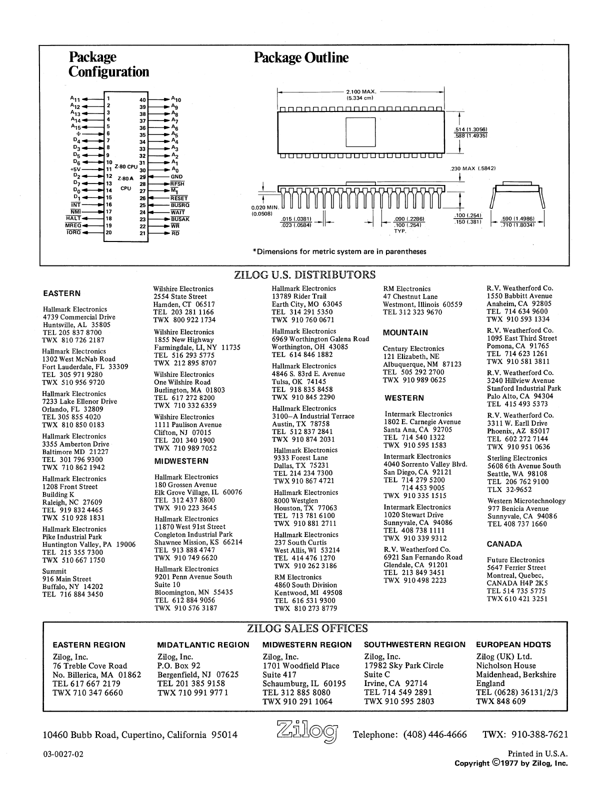
Package
Package
Outline
Configuration
I~::::
:::g
:::::
:::1
A11
40
A10
A12
39
A9
A13 3
38
A8
A14 4
37
A7
A
15
36
A6 .51411.30561
<I>
6
35
A5
.58811.49351
04 34
A4
I
03
33
Aa
05
32
A2
06
Al
+5V
AD
.230
MAX
1.58421
O2
Z·80A
GNO I
07 13
RFSH
0.02LIN
J
~
DO
CPU·
Ml
! ,
01 RESET
INT
BUSRQ
WAIT
10.05081
II
I
I--
.1001.2541
18
23 BUSAK .0151.03811 _ _ . .0901.22861
'"i5O"13siT
~
.59011.49861
_I
MREQ 19 22
WR
.023
1.05841
-.
.1001.2541
".
.71011.80341
IORQ
20
21
RD
TYP.
* Dimensions for metric system are
in
parentheses
ZILOG
U.S. DISTRJ[BUTORS
EASTERN
Hallmark Electronics
4739 Commercial Drive
Huntsville,
AL
35805
TEL
205
8378700
TWX
810726
2187
Hallmark Electronics
1302
West
McNab Road
Fort Lauderdale, FL 33309
TEL 305 971 9280
TWX
510956
9720
Hallmark Electronics
7233 Lake Ellenor Drive
Orlando, FL 32809
TEL
305
855 4020
TWX
8108500183
Hallmark Electronics
3355 Amberton Drive
Baltimore
MD
21227
TEL 301 796 9300
TWX
710862
1942
Hallmark Electronics
1208 Front Street
Building K
Raleigh,
NC
27609
TEL 919
8324465
TWX
5109281831
Hallmark Electronics
Pike Industrial Park
Huntington Valley,
PA
19006
TEL
215
355 7300
TWX
5106671750
Summit
916
Main
Street
Buffalo,
NY
14202
TEL 716 884 3450
Wilshire Electronics
2554 State Street
Hamden,
CT
06517
TEL
203
281
1166
TWX
800 922 1734
Wilshire Electronics
1855
New
Highway
Farmingdale, LI,
NY
11735
TEL
5162935775
TWX
212895
8707
Wilshire Electronics
One Wilshire Road
Burlington,
MA
01803
TEL 617 272 8200
TWX
710 332 6359
Wilshire Electronics
1111 Paulison Avenue
Clifton,
NJ
07015
TEL
201
340 1900
TWX
7109897052
MIDWESTERN
Hallmark Electronics
180 Grossen Avenue
Elk Grove Village, IL 60076
TEL
3124378800
TWX
9102233645
Hallmark Electronics
11870
West
91st Street
Congleton Industrial Park
Shawnee Mission,
KS
66214
TEL
9138884747
TWX
9107496620
Hallmark Electronics
9201 Penn A venue South
Suite 10
Bloomington,
MN
55435
TEL
6128849056
TWX
9105763187
Hallmark Electronics
13789 Rider Trail
Earth City,
MO
63045
TEL
3142915350
TWX
9107600671
Hallmark Electronics
6969 Worthingtoll Galena Road
Worthington,OH 43085
TEL
6148461882
Hallmark Electronics
4846
S.
83rd
E.
Avenue
Tulsa,
OK
74145
TEL
918835
8458
TWX
910845
2290
Hallmark Electronics
3100-A
Industrial Terrace
Austin, TX 78758
TEL
5128372841
TWX
9108742031
Hallmark Electronics
9333 Forest Lane
Dallas, TX 75231
TEL 214 234 7300
TWX
9108674721
Hallmark Electronics
8000 Westglen
Houston,
TX
77063
TEL 713
7816100
TWX
9108812711
Hallmark Electronics
237 Sou th Curtis
West Allis,
WI
53214
TEL
414476
1270
TWX
9102623186
RM
Electronics
4860 South Division
Kentwood,
MI
49508
TEL 616 531 9300
TWX
810 273 8779
RM
Electronics
47 Chestnut Lane
Westmont, Illinois 60559
TEL 312 323 9670
MOUNTAIN
Century Electronics
121
Elizabeth,
NE
Albuquerque,
NM
87123
TEL 505 292 2700
TWX
9109890625
WESTERN
Intermark Electronics
1802
E.
Carnegie Avenue
Santa Ana,
CA
92705
TEL
714540
1322
TWX
910595
1583
Intermark Electronics
4040 Sorrento Valley
Blvd.
San Diego,
CA
92121
TEL 714 279 5200
7144539005
TWX
910335
1515
Intermark Electronics
1020 Stewart
Drive
Sunnyvale,
CA
94086
TEL
408738
1111
TWX
9103399312
R.
V.
Weatherford Co.
6921 San Fernando Road
Glendale,
CA
91201
TEL
213
8493451
TWX
910498
2223
R.
V.
Weatherford
Co.
1550 Babbitt Avenue
Anaheim,
CA
92805
TEL
7146349600
TWX
910593
1334
R.V. Weatherford
Co.
1095 East Third Street
Pomona,
CA
91765
TEL
714623
1261
TWX
9105813811
R.V. Weatherford Co.
3240 Hillview Avenue
Stanford Industrial Park
Palo Alto,
CA
94304
TEL
4154935373
R.
V.
Weatherford Co.
3311
W.
Earll
Drive
Phoenix,
AZ
85017
TEL 602 272 7144
TWX
9109510636
Sterling Electronics
5608 6th Avenue South
Seattle, W A 98108
TEL 206
7629100
TLX 32-9652
Western Microtechnology
977 Benicia Avenue
Sunnyvale,
CA
94086
TEL
4087371660
CANADA
Future Electronics
5647 Ferrier Street
Montreal, Quebec,
CANADA
H4P
2K5
TEL
5147355775
TWX
6104213251
ZIJLOG SALlES
OFFICES
EASTERN REGION MIDATLANTIC REGION
Zilog, Inc. Zilog, Inc.
76
Treble Cove Road P.O. Box 92
No.
Billerica,
MA
01862
Bergenfield,
NJ
07625
TEL
617667
2179 TEL 201 385 9158
TWX
7103476660
TWX
7109919771
10460 Bubb Road, Cupertino, California 95014
03-0027-02
MIDWESTERN REGION
Zilog, Inc.
1701 Woodfield Place
Suite 417
Schaumburg,IL 60195
TEL 312
8858080
TWX 910 291 1064
SOUTHWESTERN REGION EUROPEAN HDOTS
Zilog, Inc. Zilog (UK) Ltd.
17982 Sky Park Circle Nicholson House
Suite C Maidenhead, Berkshire
Irvine,
CA
92714 England
TEL 714 549 2891 TEL (0628)
36131/2/3
TWX 910
5952803
TWX 848 609
Telephone: (408) 446-4666 1WX: 910-388-7621
Printed in U.S.A.
Copyright
©1977
by Zilog. Inc.