Cover U DV4100 14101513564522
User Manual: DV4100
Open the PDF directly: View PDF ![]() .
.
Page Count: 143 [warning: Documents this large are best viewed by clicking the View PDF Link!]

Service
Manual
Please use this service manual with referring to the user guide (D.F.U) without fail.
302W855010 AO
3120 785 22440
First Issue:2000.11
DV4100/A1B, /N1B, /S1G, /U1B
DVD Player
DV4100
TABLE OF CONTENTS
1. TECHNICAL SPECIFICATION ...............................................................................1
2. CONNECTION FACILITIES ....................................................................................3
3. INFORMATIONS ..................................................................................................... 4
4. SERVICING HINT ...................................................................................................5
5. WARNING AND LASER SAFETY INSTRUCTIONS ............................................... 6
6. SERVICE HINTS ....................................................................................................8
7. BLOCK DIAGRAM ..................................................................................................9
8. WIRING DIAGRAM ............................................................................................... 13
9. DISMANTLING INSTRUCTIONS .........................................................................15
10. EXPLODED VIEW AND PARTS LIST...................................................................17
11. SCHEMATIC DIAGRAM AND PARTS LOCATION ...............................................21
12. TROUBLESHOOTING ..........................................................................................47
13. DIAGNOSTIC SOFWARE : SCRIPT INTERFACES ............................................. 53
14. INTERACTIVE TESTS.......................................................................................... 55
15. TEST INSTRUCTIONS DISPLAY BOARD ...........................................................62
16. CURRENT MODE POWER SUPPLY 20PS203 ...................................................64
17. CIRCUIT DESCRIPTIONS AND ABBREVIATIONS.............................................. 68
18. ELECTRICAL PARTS LIST ................................................................................... 70
STOP
SOUND
PAUSE
OPEN/CLOSE
ON/OFF
STANDBY
POWER
DVD PLAYER DV4100
PLAY
Printed in Japan
DV4100
MARANTZ DESIGN AND SERVICE
Using superior design and selected high grade components, MARANTZ company has created the ultimate in stereo sound.
Only original MARANTZ parts can insure that your MARANTZ product will continue to perform to the specifications for which
it is famous.
Parts for your MARANTZ equipment are generally available to our National Marantz Subsidiary or Agent.
ORDERING PARTS :
Parts can be ordered either by mail or by Fax.. In both cases, the correct part number has to be specified.
The following information must be supplied to eliminate delays in processing your order :
1. Complete address
2. Complete part numbers and quantities required
3. Description of parts
4. Model number for which part is required
5. Way of shipment
6. Signature : any order form or Fax. must be signed, otherwise such part order will be considered as null and void.
SHOCK, FIRE HAZARD SERVICE TEST :
CAUTION : After servicing this appliance and prior to returning to customer, measure the resistance between either primary AC
cord connector pins ( with unit NOT connected to AC mains and its Power switch ON ), and the face or Front Panel of product and
controls and chassis bottom.
Any resistance measurement less than 1 Megohms should cause unit to be repaired or corrected before AC power is applied, and
verified before it is return to the user/customer.
Ref. UL Standard No. 1492.
In case of difficulties, do not hesitate to contact the Technical
Department at above mentioned address.
001120 A.O
USA
MARANTZ AMERICA, INCMARANTZ AMERICA, INC.
440 MEDINAH ROAD
ROSELLE, ILLINOIS 60172
USA
PHONE : 630 - 307 - 3100
FAX : 630 - 307 - 2687
BRAZIL
PHILIPS DA AMAZONIA IND. ELET. ITDA
CENTRO DE INFORMACOES AO
CEP 04698-970
SAO PAULO, SP, BRAZIL
PHONE : 0800 - 123123(Discagem Direta Gratuita)
FAX : +55 11 534. 8988
JAPAN
Technical
MARANTZ JAPAN, INC.
35- 1, 7- CHOME, SAGAMIONO
SAGAMIHARA - SHI, KANAGAWA
JAPAN 228-8505
PHONE : +81 42 748 1013
FAX : +81 42 741 9190
EUROPE / TRADING
MARANTZ EUROPE B.V.
P.O.BOX 80002, BUILDING SFF2
5600 JB EINDHOVEN
THE NETHERLANDS
PHONE : +31 - 40 - 2732241
FAX : +31 - 40 - 2735578
TECHNICAL AUDIO GROUP PTY, LTD
558 DARLING STREET,
BALMAIN, NSW 2041,
AUSTRALIA
PHONE : 61 - 2 - 9810 - 5300
FAX : 61 - 2 - 9810 - 5355
CANADA
LENBROOK INDUSTRIES LIMITED
633 GRANITE COURT,
PICKERING, ONTARIO L1W 3K1
CANADA
PHONE : 905 - 831 - 6333
FAX : 905 - 831 - 6936
AUSTRALIA
QualiFi Pty Ltd,
24 LIONEL ROAD,
MT. WAVERLEY VIC 3149
AUSTRALIA
PHONE : +61 - (0)3 - 9543 - 1522
FAX : +61 - (0)3 - 9543 - 3677
NEW ZEALAND
WILDASH AUDIO SYSTEMS NZ
14 MALVERN ROAD MT ALBERT
AUCKLAND NEW ZEALAND
PHONE : +64 - 9 - 8451958
FAX : +64 - 9 - 8463554
THAILAND
MRZ STANDARD CO.,LTD
746 - 754 MAHACHAI ROAD.,
WANGBURAPAPIROM, PHRANAKORN,
BANGKOK, 10200 THAILAND
PHONE : +66 - 2 - 222 9181
FAX : +66 - 2 - 224 6795
TAIWAN
PAI- YUING CO., LTD.
6 TH FL NO, 148 SUNG KIANG ROAD,
TAIPEI, 10429, TAIWAN R.O.C.
PHONE : +886 - 2 - 25221304
FAX : +886 - 2 - 25630415
MALAYSIA
WO KEE HONG ELECTRONICS SDN. BHD.
SUITE 8.1, LEVEL 8, MENARA GENESIS,
NO. 33, JALAN SULTAN ISMAIL,
50250 KUALA LUMPUR, MALAYSIA
PHONE : +60 3 - 2457677
FAX : +60 3 - 2458180
AMERICAS
SUPERSCOPE TECHNOLOGIES, INC.
MARANTZ PROFESSIONAL PRODUCTS
2640 WHITE OAK CIRCLE, SUITE A
AURORA, ILLINOIS 60504 USA
PHONE : 630 - 820 - 4800
FAX : 630 - 820 - 8103
AUSTRALIA
KOREA
MK ENTERPRISES LTD.
ROOM 604/605, ELECTRO-OFFICETEL, 16-58,
3GA, HANGANG-RO, YONGSAN-KU, SEOUL
KOREA
PHONE : +822 - 3232 - 155
FAX : +822 - 3232 - 154
SINGAPORE
WO KEE HONG DISTRIBUTION PTE LTD
130 JOO SENG ROAD
#03-02 OLIVINE BUILDING
SINGAPORE 368357
PHONE : +65 858 5535 / +65 381 8621
FAX : +65 858 6078

1
PLAYBACK SYSTEM
DVD-Video
Video CD
CD (CD-R and CD-RW)
OPTICAL READOUT SYSTEM
Lasertype Semiconductor AlGaAs
Numerical Aperture 0.60 (DVD)
0.45 (VCD/CD)
Wavelength 650 nm (DVD)
780 nm (VCD/CD)
DVD DISC FORMAT
Medium Optical Disc
Diameter 12cm (8cm)
Playing time One layer 2.15 h*
(12cm) Dual layer 4 h*
Two side 4.30 h*
Single layer
Two side 8 h*
Dual layer
TV STANDARD EUROPE USA
(PAL/50Hz) (NTSC/60Hz)
Number of lines 625 525
Playback Multistandard (PAL/NTSC)
VIDEO FORMAT
DA Converter 10 bits
Signal handling Components
Digital Compression MPEG2 for DVD,
MPEG1 for VCD
DVD
Horiz. Resolutio 720 pixels** 720 pixels**
Vertical Resolution 576 lines 480 lines
VCD
Horiz. Resolution 352 pixels 352 pixels
Vertical Resolution 288 lines 240 lines
VIDEO PERFORMANCE
Video output 1 Vpp into 75 ohm
S-Video output Y: 1 Vpp into 75 ohm
C: 0.3 Vpp into 75 ohm
RGB output 1 Vpp into 75 ohm
Black Level Shift On/Off
Video Shift Left/Right
AUDIO FORMAT
Digital MPEG Compressed Digital
DTS/AC-3
PCM 16, 20, 24 bits
fs, 44.1, 48, 96 kHz
Analog Sound Stereo
Dolby Pro Logic downmix from AC-3 multi-channel sound
3D Sound for virtual 5.1 channel sound on 2 speakers
AUDIO PERFORMANCE
DA Converter 24 bits
DVD fs 96 kHz 4 Hz - 22kHz
fs 48 kHz 4 Hz - 22 kHz
Video CD fs 48 kHz 4 Hz - 22 kHz
CD fs 44.1 kHz 4 Hz - 20 kHz
Signal-Noise (1kHz) 95 dB
Dynamic Range (1kHz) 90 dB
Crosstalk (1kHz) 110 dB
Distortion and Noise (1kHz) 85 dB
CONNECTIONS
SCART Euroconnector 2x
S-Video Output Mini DIN, 4 pins
Video Output Cinch (yellow)
Audio L+R output Cinch (white/red)
Digital Output 1 coaxial, 1 optical
IEC958 for CDDA / LPCM
IEC1937 for MPEG1/2,
AC-3 and DTS
CABINET
Dimensions(w x h x d) 440 x 92 x 305 mm
Weight Approx. 3.8 Kg
PACKAGE CONTENTS
DVD-Video Player
Remote Control & Batteries
AC Power cable
User Manual
SCART cable (Euroconnector)
Audio/Video cable
GENERAL FUNCTIONALITY
Stop / Play / Pause
Fast Forward / Backward
Time search
Step Forward / Backward
Slow
Title / Chapter / Track Select
Skip Next / Skip Previous
Repeat (Chapter / Title / All) or (Track / All)
A-B Repeat
Shuffle
Enhanced ease of use graphical interface
Perfect Still with digital multi-tap filter
Zoom (x1.33, x2, x4) with picture enhancement
3D Sound
Virtual jog shuttle
Audio and video bit rate indicator
(only available in certain countries)
DVD FUNCTIONALITY
Multi-angle Selection
Audio Selection (1 out of max. 8 languages)
Subtitles Selection (1 out of max. 32 languages)
Aspect Ratio conversion (16:9, 4:3 Letterbox, 4:3 Pan Scan)
Parental Control and Disk Lock
Disc Menu support (Title Menu and Root Menu)
Resume (5 discs) after stop / standby
Screen Saver (Dim 75% after 15 min.)
Programming Titles/chapters with Favorite Selection
VIDEO CD FUNCTIONALITY
Playback Control for VCD 2.0 discs
Parental Control and Disc lock
Resume (5 discs) after stop / standby
Screen Saver (Dim 75% after 15 min.)
Programming Tracks with Favorite Selection
AUDIO CD FUNCTIONALITY
Time Display (Total / Track )
Full audio functionality with remote control
Programming with Favorite Track Selection
* typical playing time for movie with 2 spoken languages and 3 subtitle languages.
** equivalent to 500 lines on your TV
Specifications subject to change without prior notice
1. TECHHNICAL SPECIFICATIONS (/N1B)

PLAYBACK SYSTEM
DVD-Video
Video CD
CD (CD-R and CD-RW)
OPTICAL READOUT SYSTEM
Lasertype Semiconductor AlGaAs
Numerical Aperture 0.60 (DVD)
0.45 (VCD/CD)
Wavelength 650 nm (DVD)
780 nm (VCD/CD)
DVD DISC FORMAT
Medium Optical Disc
Diameter 12cm (8cm)
Playing time One layer 2.15 h*
(12cm) Dual layer 4 h*
Two side 4.30 h*
Single layer
Two side 8 h*
Dual layer
TV STANDARD EUROPE USA
(PAL/50Hz) (NTSC/60Hz)
Number of lines 625 525
Playback Multistandard (PAL/NTSC)
VIDEO FORMAT
DA Converter 10 bits
Signal handling Components
Digital Compression MPEG2 for DVD,
MPEG1 for VCD
DVD
Horiz. Resolution 720 pixels* 720 pixels**
Vertical Resolution 576 line 480 lines
VCD
Horiz. Resolution 352 pixel 352 pixels
Vertical Resolution 288 line 240 lines
VIDEO PERFORMANCE
Video output 1 Vpp into 75 ohm
S-Video output Y: 1 Vpp into 75 ohm
C: 0.3 Vpp into 75 ohm
Y 1 Vpp into 75 ohm
C
R
0.7 Vpp into 75 ohm
C
B
0.7 Vpp into 75 ohm
Black Level Shift On/Off
Video Shift Left/Right
AUDIO FORMAT
Digital MPEG Compressed
DTS/AC-3
PCM 16, 20, 24 bits
fs, 48, 96 kHz
Analog Sound Stereo
Dolby Pro Logic downmix from AC-3 multi-channel sound
3D Sound for virtual 5.1 channel sound on 2 speakers
AUDIO PERFORMANCE
DA Converter 24 bits
DVD fs 96 kHz 4 Hz - 44 kHz
fs 48 kHz 4 Hz - 22 kHz
Video CD fs 48 kHz 4 Hz - 22 kHz
CD fs 44.1 kHz 4 Hz - 20 kHz
Signal-Noise (1kHz) 95 dB
Dynamic Range (1kHz) 90 dB
Crosstalk (1kHz) 110 dB
Distortion and Noise (1kHz) 85 dB
CONNECTIONS
S-Video Output Mini DIN, 4 pins
Component Video Y Cinch (green)
U (C
R
) Cinch (blue)
V (C
B
) Cinch (red)
Video Output Cinch (yellow) 2x
Audio L+R output Cinch (white/red) 2x
Digital Output 1 coaxial, 1 optical
IEC958 for CDDA / LPCM
IEC1937 for MPEG1/2,
AC-3 and DTS
CABINET
Dimensions (w x h x d) 440 x 92 x 305mm
Weight Approx. 3.8 Kg
PACKAGE CONTENTS
DVD-Video Player
Remote Control & Batteries
AC power cord
User Manual
Audio/Video cord
GENERAL FUNCTIONALITY
Stop / Play / Pause
Fast Forward / Backward
Time search
Step Forward / Backward
Title / Chapter / Track Select
Skip Next / Skip Previous
Repeat (Chapter / Title / All) or (Track / All)
A-B Repeat
Shuffle
Enhanced ease of use graphical interface
Perfect Still with digital multi-tap filter
Zoom (x1.33 x2. x4) with picture enhancement
3D Sound
Virtual Jog Shuttle
Audio and video bit rate indicator
(only available in certain countries)
DVD FUNCTIONALITY
Multi-angle Selection
Audio Selection (1 out of max. 8 languages)
Subtitles Selection (1 out of max. 32 languages)
Aspect Ratio conversion (16:9, 4:3 Letterbox, 4:3 Pan Scan)
Parental Control and Disk Lock
Disc Menu support (Title Menu and Root Menu)
Resume (5 discs) after stop / standby
Screen Saver (Dim 75% after 15 min.)
Programming Titles/chapters with Favorite Selection
VIDEO CD FUNCTIONALITY
Playback Control for VCD 2.0 discs
Parental Control and Disc lock
Resume (5 discs) after stop / standby
Screen Saver (Dim 75% after 15 min.)
Programming Tracks with Favorite Selection
AUDIO CD FUNCTIONALITY
Time Display (Total / Track )
Full audio functionality with remote control
Programming with Favorite Track Selection
* typical playing time for movie with 2 spoken languages and 3 subtitle languages.
** equivalent to 500 lines on your TV
Specifications subject to change without prior notice
2
(/A1B, /S1G, /U1B)
1 2
2
2
5
5
4
4
3
6
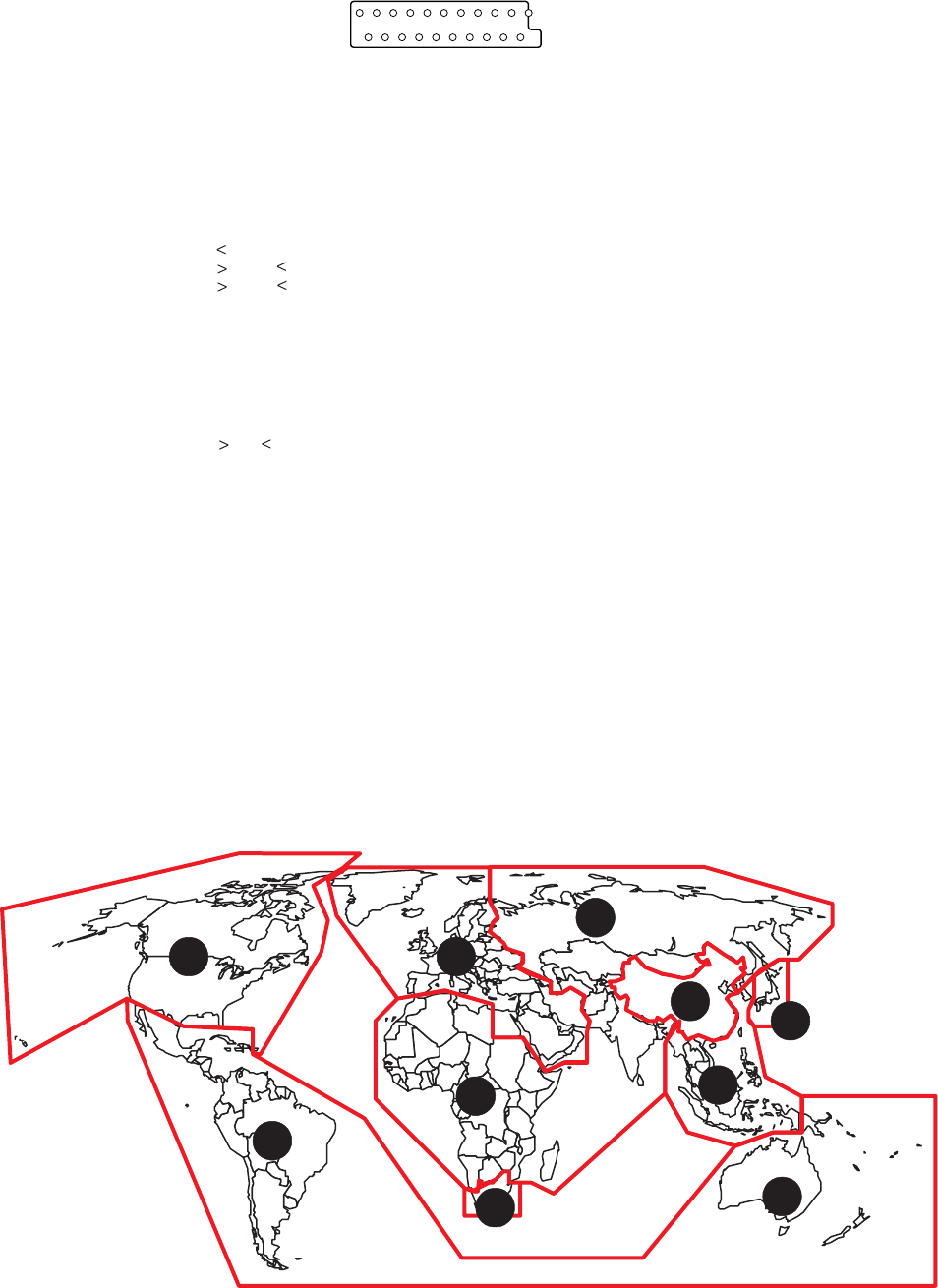
Map of DVD Regions
What are "regional codes"?
Motion picture studios want to control the home release of movies in different countries because theater releases arenít
simultaneous (a movie may come out on DVD in the US when itís just hitting screens in Europe). Therefore they have
required that the DVD standard include codes which can be used to lock out the playback of certain discs in certain geo-
graphical regions. Players sold in each region will have that regionís code built into the player. The player will refuse to play
these "region coded" discs which are not allowed in the region. However, regional codes are entirely optional. Discs without
codes will play on any player in any country. Some studios have already announced that only their new releases will have
regional codes. There are six regions:
1. United States and Canada
2. Europe and Japan
3. Far East (except Japan & China)
4. South America and Oceania
5. Africa and the Middle East
6. China (except Hong Kong)
3
2. CONNECTION FACILITIES
1 3 5 7 9 11 13 15 17 19
21
2 4 6 8 10 12 14 16 18 20
2-1 Video performance (/N1B only)
SCART (/N1B versions only)
Full according PQR3 IMS
Connector implementation according EN50049-1; color = black; dual SCART
Fully according to prEN1057-2-1
Signal switching is P50 controlled; supported features of mode 3 see survey of applicable standards.
2-1-1 SCART II (connected to TV)
Pin signals:
1 Output Audio R 1.8V RMS
2 Input Audio R
3 Output Audio L 1.8V RMS
4 Audio GND
5 Blue/Chroma GND
6 Input Audio L
7 Bi-dir Blue out/Chroma in 0.7pp +/-0.1V into 75 Ohm (*)
8 Output Function switch 2V = TV
4.5V / 7V = asp. ratio 16:9 DVD
9.5V / 12V = asp. ratio 4:3 DVD
9 Green GND
10 Bi-dir P50 control
11 Output Green 0.7Vpp +/-0.1V into 75 Ohm (*)
12 not connected
13 Red/Chroma GND
14 fast switch GND
15 Output Red out/Chroma out 0.7Vpp +/-0.1V into 75 Ohm (*)
+/-3dB 0.3Vpp in case of Chroma
16 Output fast switch RGB 1V / 3V into 75 Ohm = RGB
/CVBS or Y
0.4V into 75 Ohm = CVBS
17 Y/CVBS GND
18 fast switching GND
19 Output CVBS/Y/RGB sync 1Vpp +/-0.1V into 75 Ohm (*)
20 Input CVBS/Y
21 Shield
SCART I (connected to AUX)
Pin signals:
1 Output Audio R 1.8V RMS
2 Input Audio R
3 Output Audio L 1.8V RMS
4 Audio GND
5 Blue/Chroma GND
6 Input Audio L
7 Bi-dir Blue in/Chroma out +/-3dB 0.3Vpp Chroma
8 Input Function switch
9 Green GND
10 Bi-dir P50 control
11 Input Green
12 not connected
13 Red/Chroma GND
14 fast switch GND
15 Input Red in/Chroma in
16 Input fast switch RGB/CVBS or Y
17 CVBS GND
18 fast switching GND
19
20 Input CVBS/Y
21 Shield
(*) for 100% white
4
3. INFORMATIONS
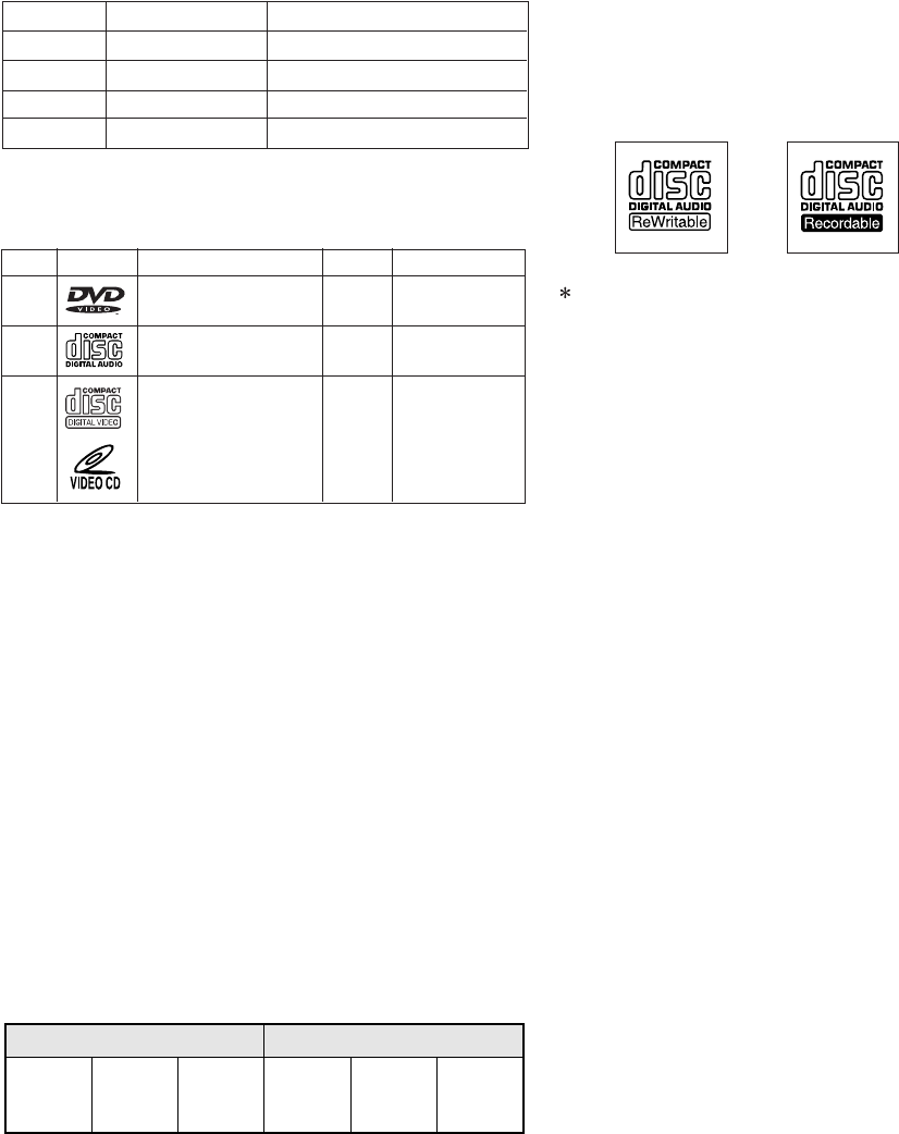
REGION CODE
THE DISCS THAT THE DV4100 CAN HANDLE
The following discs can be played back with a DV4100.
Note: The regional code of the discs must meet to the regional
code of the DV4100.
DVD INFORMATION
Below is a glossary of the new terms related to DVD.
Title:
A disc may have more than one story/movie on it, so each
story/movie is called a “title”.
For example, if there are 2 movies on the disc, they are
separated into Title 1 and Title 2.
Chapter:
A title may also be separated into chapters.
For example, a movie (title) may be separated into 3 scenes
(chapters).
Subtitles:
DVDs are recorded with up to 32 different subtitle languages.
If a disc has more than one subtitle language, you can select
the subtitle language that you want to read.
Soundtrack language:
DVDs are recorded with up to 8 different soundtrack languages.
If a disc has more than one language, you can select the
soundtrack language that you want to listen to.
disc mark playback capability size side
DVD Audio/Video 12 cm single/double
8 cm
CD Audio 12 cm single
8 cm
12 cm
VCD Audio/Video single
8 cm
VERSION REGION CODE COUNTRY
/N1B 2 EUROPE
/S1G 3 ASIAN PACIFIC
/U1B 1 USA/CANADA
/A1B 4 AUSTRALIA
Multi-angles:
On some DVDs, scenes have been filmed from different angles
(up to a maximum of 9). On these discs, you can select the
angle that you want to watch. Please refer to the DVD’s manual
to see which scenes have multi-angles.
Title 1 Title 2
Chapter
3Chapter
1Chapter
2Chapter
3
Chapter
1Chapter
2
It is important to note that CD-R, CD-RW discs must be
FINALIZED before they can be played on this player. The disc
types which run on the player feature one or more of these
logos on the disc packaging.
5
4. SERVICING HINT
SERVICE TOOLS
Audio signals disc 4822 397 30184
Disc without errors (SBC444)+
Disc with DO errors, black spots and fingerprints (SBC444A) 4822 397 30245
Disc (65 min 1kHz) without no pause 4822 397 30155
Max. diameter disc (58.0 mm) 4822 397 60141
Torx screwdrivers
Set (straight) 4822 395 50145
Set (square) 4822 395 50132
13th order filter 4822 395 30204
DVD test disc
TEST software for PC : ComPair V1. 2
ComPair V1. 3
Connection Cable
4822 397 10131
4822 727 21634
4822 727 21637
3122 785 90017
SERVICE HINTS
6
5. WARNING AND LASER SAFETY INSTRUCTIONS
SHOCK, FIRE HAZARD SERVICE TEST:
CAUTION: After servicing this appliance and prior to returning to customer, measure the resistance between
either primary AC cord connector pins (with unit NOT connected to AC mains and its Power switch ON), and the
face or Front Panel of product and controls and chassis bottom,
Any resistance measurement less than 1 Megohms should cause unit to be repaired or corrected before AC
power is applied, and verified before return to user/customer.
Ref.UL Standard NO.1492.
NOTE ON SAFETY:
Symbol : Fire or electrical shock hazard. Only original parts should be used to replace any part with symbol
Any other component substitution(other than original type), may increase risk or fire or electrical shock hazard.
FATTENTION
Tous les IC et beaucoup d’autres semi-
conducteurs sont sensibles aux décharges
statiques (ESD).
Leur longévité pourrait être considérablement
écourtée par le fait qu’aucune précaution
n’est prise a leur manipulation.
Lors de réparations, s’assurer de bien être
relié au même potentiel que la masse de
l’appareil et enfiler le bracelet serti d’une
résistance de sécurité.
Veiller a ce que les composants ainsi que les
outils que l’on utilise soient également a ce
potentiel.
DWARNUNG
Alle IC und viele andere Halbleiter sind
empfindlich gegen elektrostatische
Entladungen (ESD).
Unsorgfältige Behandlung bei der Reparatur
kann die Lebensdauer drastisch vermindern.
Sorgen sie dafür, das Sie im Reparaturfall
über ein Pulsarmband mit Widerstand mit
dem Massepotential des Gerätes verbunden
sind.
Halten Sie Bauteile und Hilfsmittel ebenfalls
auf diesem Potential.
WAARSCHUWING
Alle IC’s en vele andere halfgeleiders zijn
gevoelig voor elektrostatische ontladingen
(ESD).
Onzorgvuldig behandelen tijdens reparatie
kan de levensduur drastisch doen
verminderen.
Zorg ervoor dat u tijdens reparatie via een
polsband met weerstand verbonden bent met
hetzelfde potentiaal als de massa van het
apparaat.
Houd componenten en hulpmiddelen ook op
ditzelfde potentiaal.
AVVERTIMENTO
Tutti IC e parecchi semi-conduttori sono
sensibili alle scariche statiche (ESD).
La loro longevita potrebbe essere fortemente
ridatta in caso di non osservazione della piu
grande cauzione alla loro manipolazione.
Durante le riparazioni occorre quindi essere
collegato allo stesso potenziale che quello
della massa dell’apparecchio tramite un
braccialetto a resistenza.
Assicurarsi che i componenti e anche gli
utensili con quali si lavora siano anche a
questo potenziale.
All ICs and many other semi-conductors are
susceptible to electrostatic discharges (ESD).
Careless handling during repair can reduce
life drastically.
When repairing, make sure that you are
connected with the same potential as the
mass of the set via a wrist wrap with
resistance.
Keep components and tools also at this
potential.
WARNING
Safety regulations require that the set be restored to its original condition
and that parts which are identical with those specified be used.
Veiligheidsbepalingen vereisen, dat het apparaat in zijn oorspronkelijke
toestand wordt terug gebracht en dat onderdelen, identiek aan de
gespecifieerde worden toegepast.
Bei jeder Reparatur sind die geltenden Sicherheitsvorschriften zu beachten.
Der Originalzustand des Gerats darf nicht verandert werden.
Fur Reparaturen sind Original-Ersatzteile zu verwenden.
Le norme di sicurezza esigono che l’apparecchio venga rimesso nelle
condizioni originali e che siano utilizzati pezzi di ricambiago idetici a quelli
specificati.
Les normes de sécurité exigent que l’appareil soit remis a l’état d’origine et
que soient utilisées les pièces de rechange identiques à celles spécifiées.
GB NL
I
D
I
F
GB
NL
7
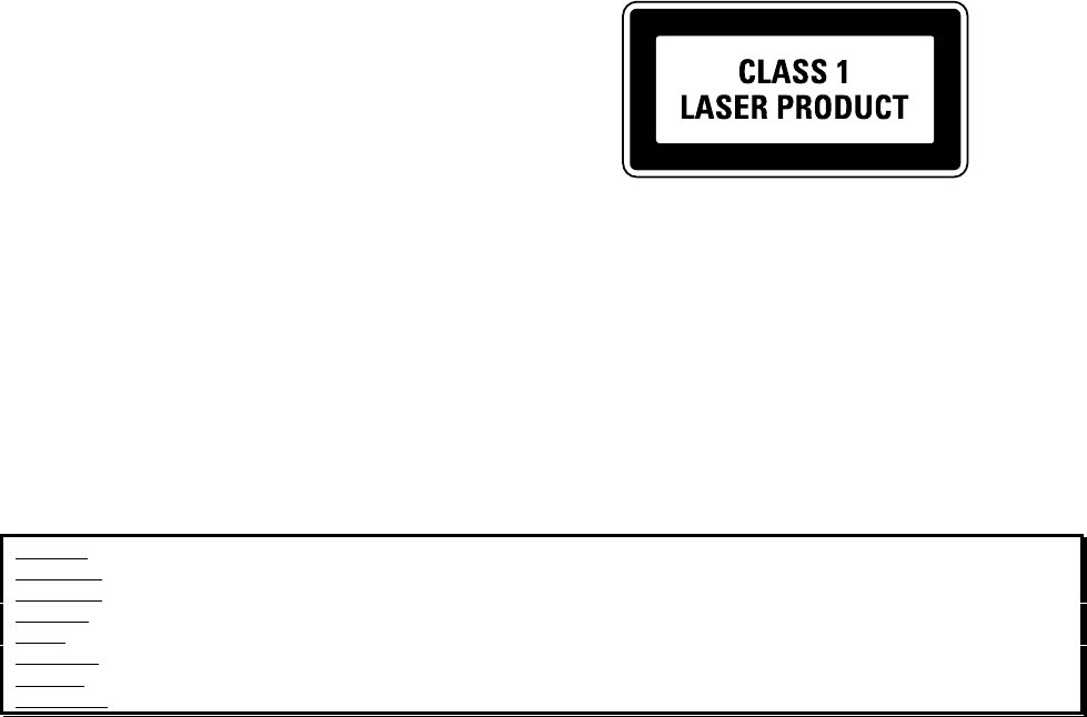
LASER SAFETY
This
this unit employs a laser. Only a qualified service person should remove the cover or attempt to service
device, due to possible eye injury.
LASER DEVICE UNIT
Type: Semiconductor laser GaAlAs
Wave length: 650 nm (DVD)
780 nm (VCD/CD)
Output Power: 7 mW (DVD)
10 mW (VCD/CD)
Beam divergence: 60 degree
USE OF CONTROLS OR ADJUSTMENTS OR PERFORMANCE OF PROCEDURE OTHER THAN
THOSESPECIFIED HEREIN MAY RESULT IN HAZARDOUS RADIATION EXPOSURE.
AVOID DIRECT EXPOSURE TO BEAM
WARNING
The use of optical instruments with this product will increase eye hazard.
Repair handling should take place as much as possible with a disc loaded inside the player
WARNING LOCATION: INSIDE ON LASER COVERSHIELD
CAUTION VISIBLE AND INVISIBLE LASER RADIATION WHEN OPEN AVOID EXPOSURE TO BEAM
ADVARSEL SYNLIG OG USYNLIG LASERSTRÅLING VED ÅBNING UNDGÅ UDSÆTTELSE FOR STRÅLING
ADVARSEL SYNLIG OG USYNLIG LASERSTRÅLING NÅR DEKSEL ÅPNES UNNGÅ EKSPONERING FOR STRÅLEN
VARNING SYNLIG OCH OSYNLIG LASERSTRÅLNING NÄR DENNA DEL ÄR ÖPPNAD BETRAKTA EJ STRÅLEN
VARO! AVATT AESSA OLET ALTTIINA NÄKYVÄLLE JA NÄKYMÄTTÖMÄLLE LASER SÄTEILYLLE. ÄLÄ KATSO SÄTEESEEN
VORSICHT SICHTBARE UND UNSICHTBARE LASERSTRAHLUNG WENN ABDECKUNG GEÖFFNET NICHT DEM STRAHL AUSSETSEN
DANGER VISIBLE AND INVISIBLE LASER RADIATION WHEN OPEN AVOID DIRECT EXPOSURE TO BEAM
ATTENTION RAYO NNEMENT LASER VISIBLE ET INVISIBLE EN CAS D'OUVERTURE EXPOSITION DANGEREUSE AU FAISCEAU
Warning for powersupply on position 1005
The primary side of the powersupply including the heatsink carrieslive mains voltage when the
player is connected to the mains even when the player is swiched off !
This primary area is not shielded so it is possible to touc h copper tracks and/or components when
servicing the player. Service personnel have to take precautions to prevent touching this area or
components in this area .
The primary side of the powersupply has been indicated with a lightning stroke and a stripe-marked
printed on the printed wiring board
Note:
The screws on the basic Engine (position 218 in on the exploded view drawing) may never be
touched removed or re-adjusted.
Handle the Basic engine with care when the unit has to be exchanged!
The mechanism of the basic engine is very sensative for droping or shocks
!

6. SERVICE HINTS
8
6.1 DVD-Module 218
The DVD mechanism has to be exchanged completely in case
of failure. A new or repaired mechanism can be ordered with
codenumber 9305 023 61001.
Return the defective unit complete assembled in original
package to Philips Consumer Service in Eindhoven.
The monoboard has to be repaired on component level.
6.2 Diagnostic software
In chapter “Diagnostic software” some tests are refering to the
SCART functionality.
These tests are for sets with RGB-output.
For sets without RGB-output no SCART connector is mounted.
In these sets the SCART tests will automatically be skipped
6.3 Power Supply options
6.4 Compair
For assistance with the repair process of the monoboard an
electronic Fault finding guidance has been developed , this
program is called COMPAIR.
This COMPAIR program is available on CDROM.
The Version of the CDROM for repair of the monoboard is V1.3
and can be ordered with codenumber : 4822 727 21637.
This is an update CDROM , so when the COMPAIR CDROM is
used for the first time , one has to install the COMPAIR
ENGINE CDROM V1.2 first.
The V1.2 CDROM can be ordered with codenumber 4822 727
634 and has to registered after installation , the procedure for
registration is explained in the help file of the program and in
the booklet from the CDROM.
The cable to connect the monoboard with a PC can be ordered
with codenumber 3122 785 90017.
All the hardware and software requirements of the systems
necessary for working with COMPAIR is described on the
CDROM.
6.5 Monoboard repair
For repair of the monoboard the service manual 3122 785
10045 must be used.
3122 427 21750 3122 427 21370 3122 427 21760
110V USA 220V Europe China Multi voltage A/P
2261 CAP 330pF 2121 ELCO 100uF 385V 2261 CAP 330pF
2121 ELCO 150uF 250V 2121 ELCO 150uF 400V
3133 Resistor 10M
910
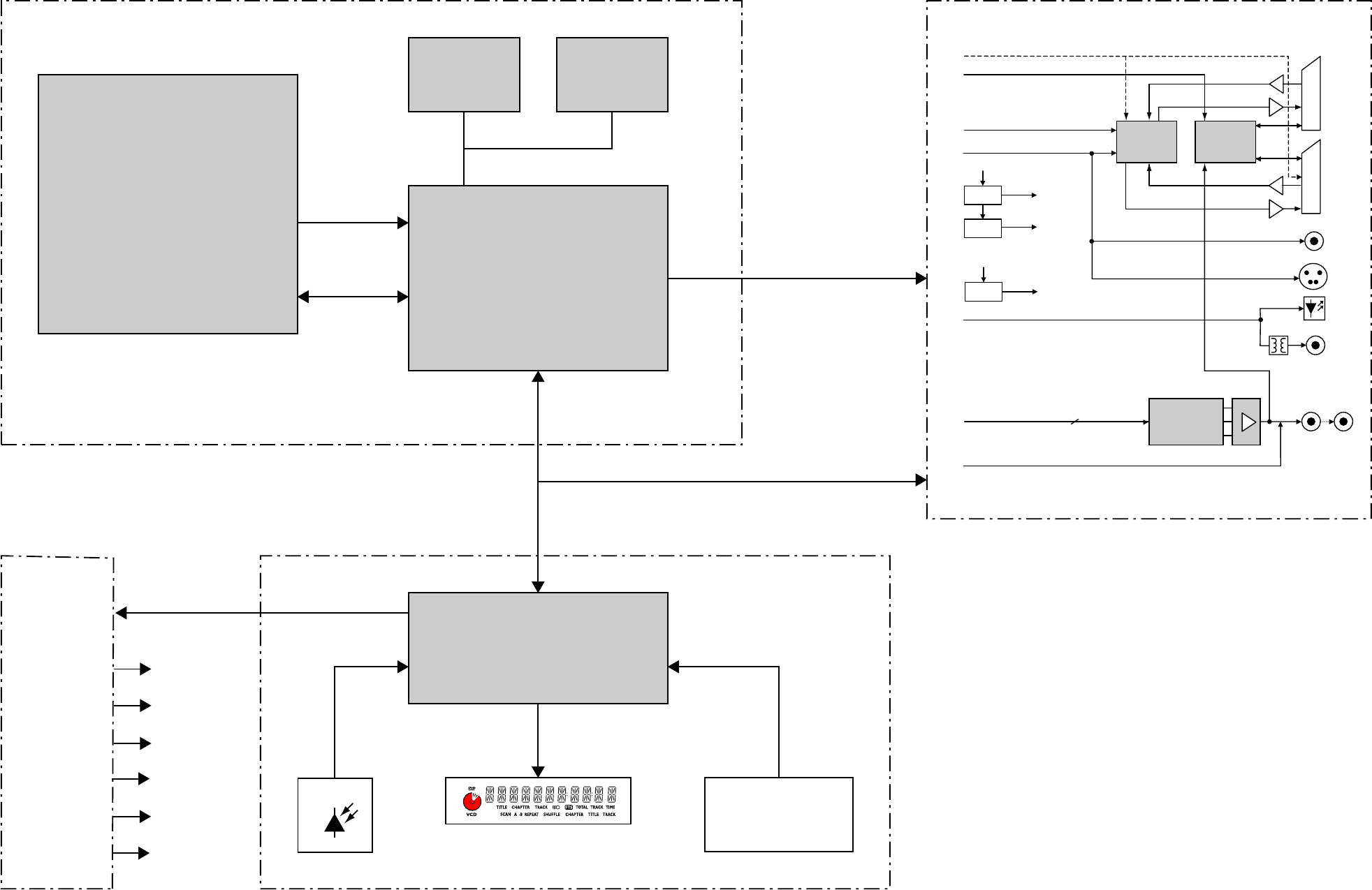
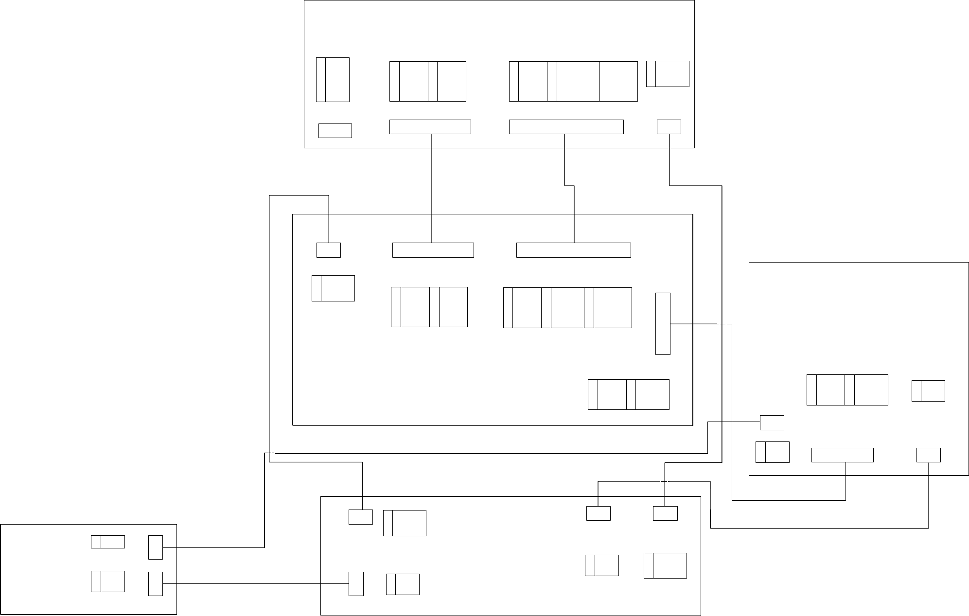
7. BLOCK DIAGRAM (/N1B)
SLAVE PROCESSOR
KEYBOARD
SPMS
St_by
AUDIO/VIDEO BACKEND BOARD
JBE
(servo)
RAM ROM
HOST
Sti5505
I2S
S2B
MONO BOARD
A/V signals
I2C
SCART
SWITCHING
AUX
TV
Y/C
CVBS(/YC not on SCART)
CVBS
CVBS
0/6/12V
RGB
UDA1328T
3
Kill
8Vstab
3V3stab
+12Vstby
Video
IC's and
audio
buffers
DAC
RGB/CVBS
RGB/CVBS
CVBS
AUDIO
AUDIO
AUDIO
L + R
DAC
SCART
SCART
DISPLAY BOARD
RGB/CVBS
L+R
I2C
DIG_OUT
I2S Audio
-5Vstab
-8Vstby
Switches
OPTICAL
OUTPUT
DIGITAL
OUTPUT
RC
7104
1113
TEA6420
AUDIO SCART
SWITCHING
7917
7401 7403
7900-7905
+12V stby
+5V stby
-8V stby
-40V
+5V
+3V3
11 12
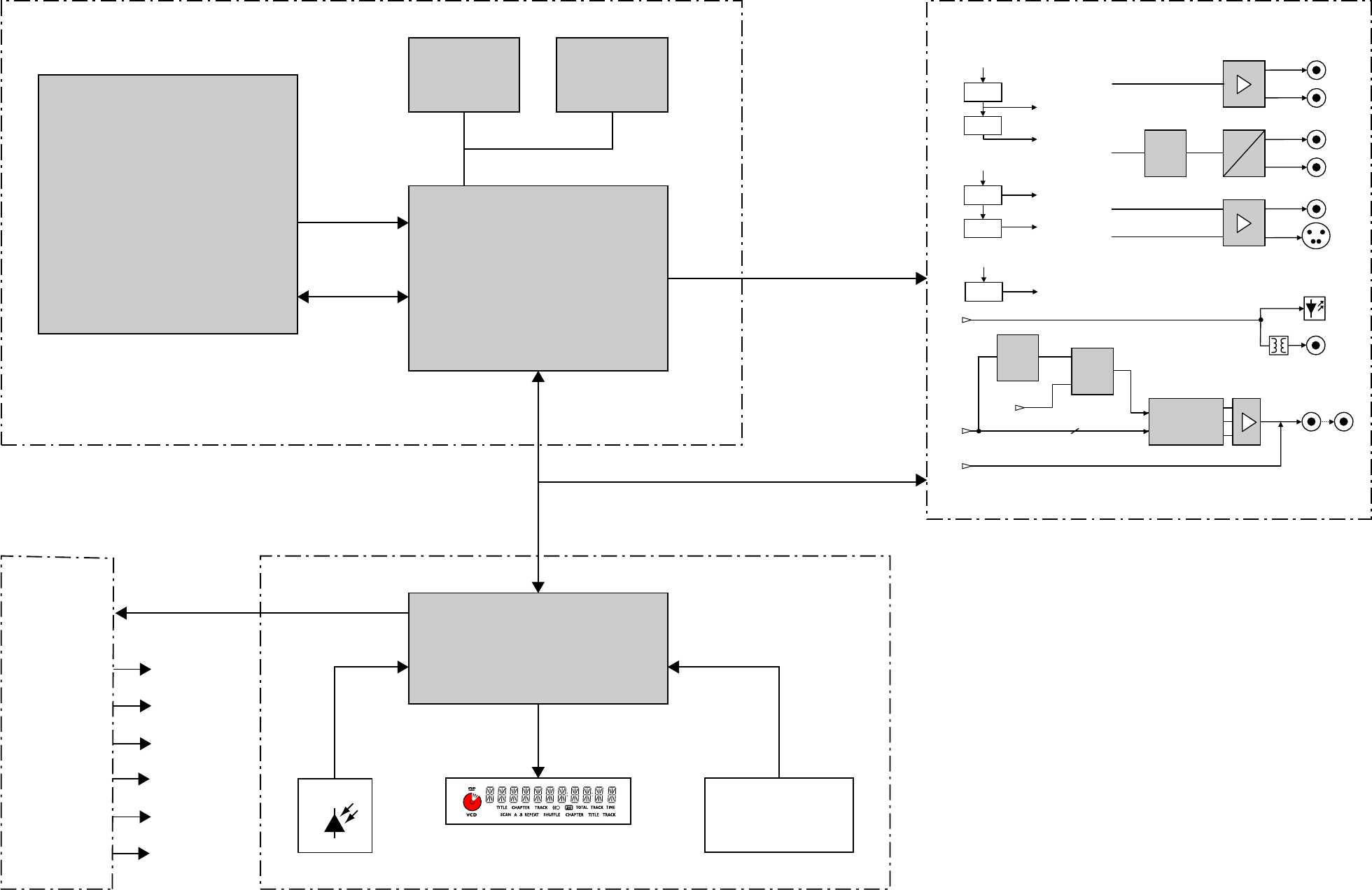
(/A1B, /S1G, /U1B)
SLAVE PROCESSOR
KEYBOARD
SPMS St_by
AUDIO/VIDEO BACKEND BOARD
JBE
(servo)
RAM ROM
HOST
Sti5505
I2S
S2B
MONO BOARD
A/V signals
I2C
Y/C
Y
UDA1328T
3
KILL
8Vstab
3V3stab
+12Vstby
Video
IC's and
audio
buffers
DAC
Headphone out
L + R
(ONLY DVD751)
2x
DAC
DISPLAY BOARD
DIG_OUT
I2S Audio
MICRO
-5Vstab
-8Vstby
Switches
-8V
-5V
-8V
OPTICAL
OUTPUT
DIGITAL
OUTPUT
RC
7104
1113
7400
7405 # # DVD732 ONLY
7403 #
7008
7002
CVBS1
CVBS
RGB
Y
C
CVBS2
7020 : 7023
+12V stby
+5V stby
-8V stby
-40V
+5V
+3V3
CB
CR
TDA 4780
KOK
TC9409
-5V
13 14
8. WIRING DIAGRAM
Non Euro model only
EH
1
2
20
1
2STBKEY+
STBKEY-
105MM -----> 105MM -----> 400MM ----->
3139 110 38371
----->
100MM
3139 110 37201
----->
400MM
Non Euro model only
5
ADJA_OUT
ADJA_IN
ADJB_OUT
1
2
3
4
5
6
7
HP_L
MIC GND
HP_R
+12V
MIC_A
EH
GND
+12V
GND
+5VSTBY
STBKEY-
EH EH
EH
PH
*
4
1
1205
1
2
3
4
+5VSTBY
STBLED
STBKEY+
STBKEY-
STANDBY
BOARD
4
1115 15 1116
1
2
4
GND
C
GND
Y
ADJB_IN
MIC GND
DISPLAY
BOARD
1
4
1117
1
2
3
4
+12V
GND
+5VSTBY
-40V
1
2
3
4
+5V
+5VSTBY
+6VSTBY
GND
GND
GND
-8VSTBY
2
+12VSTBY
CENTER_ON
STEREO_MUTE
DIG_OUT
GND
1
2
3
4
5
6
7
8
9
10
11
12
1
2
3
4
0207
3V3
3V3
PCM_OUT2
GND
PCM_OUT1
-8VSTBY
SCL
+12VSTBY
SDA
STBCONTROL
3V3A
9
10
11
12
1
2
3
4
5
6
7
8
9
10
11
12
3V3
3V3
+5V
+5VSTBY
+6VSTBY
GND
GND
+5VD
+5WD
KILL
GND
PCM_OUT0
LRCLK
SCLK
FFC
PCM_CLK
MIC GND
1
2
31
2
3
4
5
6
7
8
9
10
11
12
13
14
15
16
GND
H_SYNC
GND
MONO BOARD
1
2
3
4
5
6
+6VSTBY
8
CVBS
GND
0|6|12
-8V
13
14
15
16
17
18
19
20
21
22
P50
B
G
GND
R
CVBS
GND
0|6|12
-8V
1
2
3
4
5
ADJA_OUT
ADJA_IN
GND
ADJB_IN
8 1
16 1
4
5
15 116 122
1
12
1501 1604 1603
1600
SCL
GND
SCA
STBCONTROL
P50
GND
C
GND
Y
P50
B
G
7
R
280MM
GND
-8V
8
+5VD
+5WD
KILL
GND
PCM_OUT0
LRCLK
SCLK
GND
PCM_CLK
CENTER_ON
STEREO_MUTE
DIG_OUT
GND
A/V BOARD
EH
EH FFC FFC
*
15
16
17
18
19
20
21
ADJB_OUT
122 15
1002 1000 1001 1003
GND
H_SYNC
GND
PCM_OUT2
GND
PCM_OUT1
-8VSTBY
SCL
+12VSTBY
SDA
+6VSTBY
3V3A
1
2
3
4
5
6
7
GND
<-----
1
GND
-8VSTBY
STBCONTROL
KILL 8
9
10
11
12
13
14
15
16
1
2
3
4
5
6
7
8
9
10
11
12
13
14 22
PH
5
SCL
GND
SCA
STBCONTROL
P50
1
3
4
+5VSTBY
STBLED
-40V
POWER SUPPLY
BOARD
EHHR
41
0205 121
3
FFCPH
GND
+12VSTBY
15 1118
<----- 280MM
<----- 400MM
----->
100MM
3139 110 38831
3139 110 34221
3139 110 34321
3103 308 91150
3139 110 38631
3139 110 38681
3139 110 34251
STBKEY+
1
2
STBKEY+
STBKEY -
EH
1
2 CN4
15 16
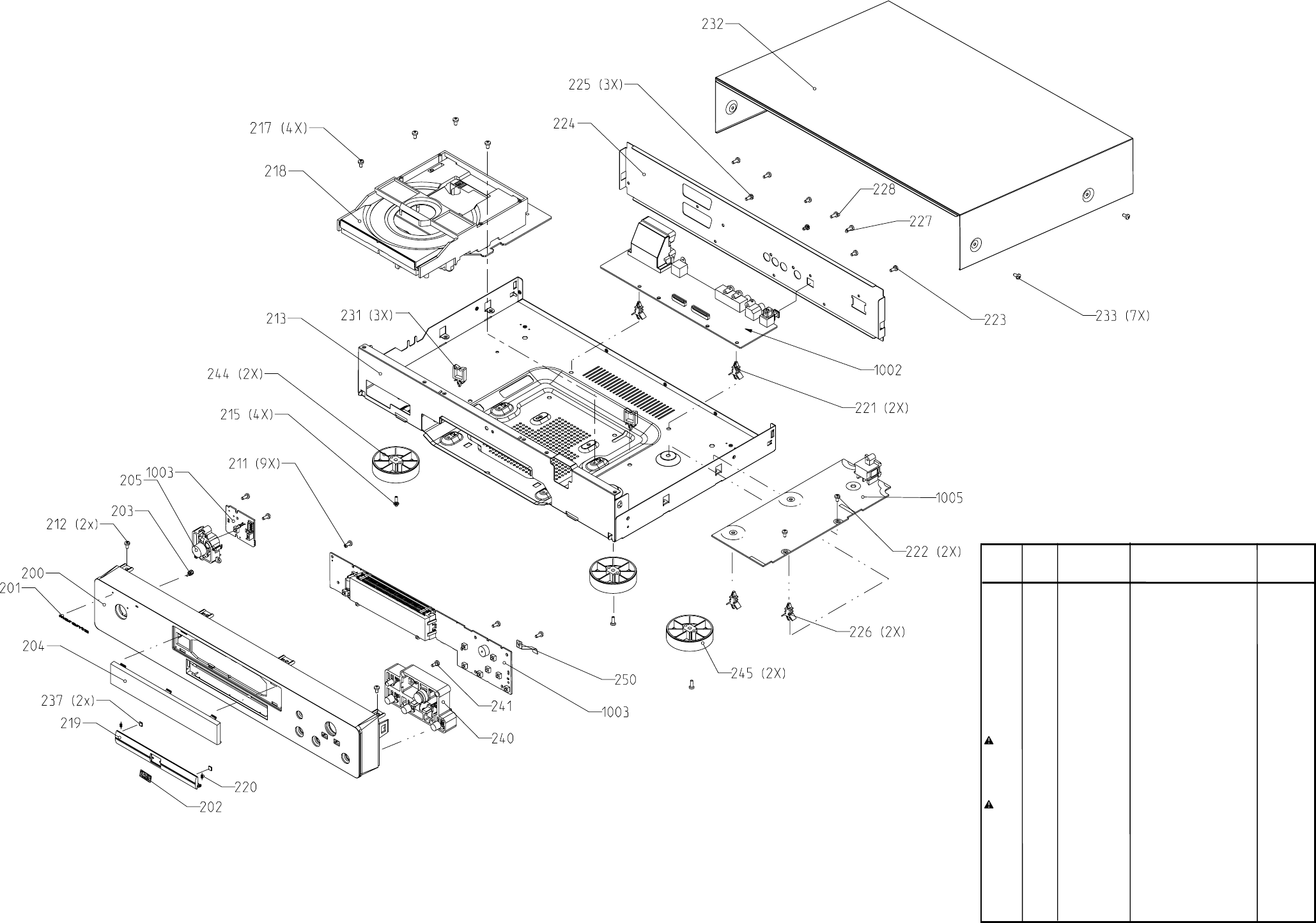
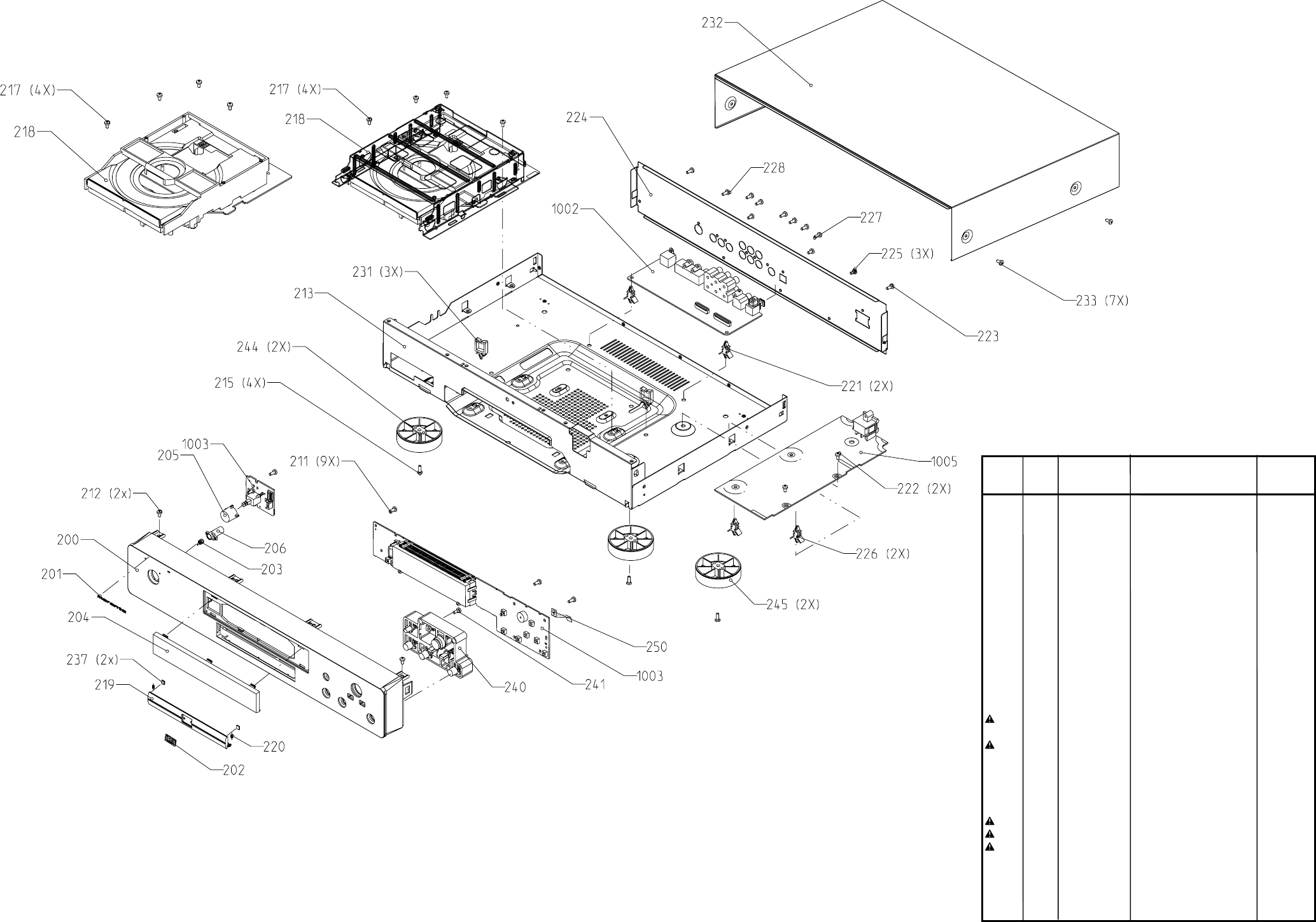
9. DISMANTLING INSTRUCTIONS
Cover 151
Remove 7 screws 233
Lift cover at rearside to
remove
Front assy 1
remove 2 screws 212
(front 1 frame 213)
unlock front from frame by
releasing successively 3
snaps (on the left, in the
middle and on the right)
put front assy in front of the
set(service position)
DVD MODULE 218
Remove connections to
Mono board
remove 4 screws
217 (loader bracket
2 frame 213)
demount module
DVD MONO Board 7
See also exploded view of
DVD module
Remove flex connections to
turntable motor and sledge
motor.
remove 4 screws
10 13(mono board 7
loader bracket 2)
remove carefully flex
connection to OPU and wire
connection to tray motor.
demount board.
LOADER VAL3000 1
Remove 2 screws 8,9
Remove 4 suspensions
3 6 from loader bracket
Standby board 1003 and
switch assy
Remove 2 screws
25 26(board front)
demount board
Remove 1 screw 207
Take out switch assy
Display board 1002
Remove 7 screws
203(board front), pay
attention to earth spring 300.
demount board
AV board 1002
remove flex connections to
Mono board
remove 7 screws 227
release snaps of 2 spacers
221
demount board
Power supply unit 1005
remove connections
remove 2 screws 222
(board frame)
remove screw 225 (mains
inled backplate)
release snaps of spacers
226 (board frame)
demount board
mounting
demounting
17 18
10. EXPLODED VIEW AND PARTS LIST (/N1B)
POS.
NO VERS.
COLOR PART NO.
(PCS) DESCRIPTION PART NO.
(MJI)
0200 3139 247 51280 FRONT PANEL (BLACK) QT24751280
0201 3120 001 00051 BADGE MARANTZ QZ00100051
0202 3139 247 51310 BADGE DVD QT24751310
0204 3139 244 00550 WINDOW QT24400550
0205 3139 244 00560 BUTTON STANDBY QT24400560
0219 3139 244 00590 DOOR QT24400590
0220 3139 241 20110 SPRING DOOR QT24120110
0240 3139 247 51410 BUTTON CONTROL QT24751410
0244 3139 247 51461 FOOT QT24751461
0245 3139 247 51461 FOOT QT24751461
1005 3122 427 22300 PSU PCB ASSY
DVD2B+ 20PS223
1014 3104 157 11190 CWAS FLEX DVD 22 130 32S QW15711190
1018 3104 157 11200 CWAS FLEX DVD 16 130 32S QW15711200
0385 4822 321 10249 MAINS CORD QP32110249
0384 3139 228 85500 REMOTE CONTROL QT22885500
0387 3139 246 10340 USER GUIDE (/N1B) QT24610340
19 20
(/A1B, /S1G, /U1B)
For /A1B, /S1G and /U1B new
For /U1B old
POS.
NO VERS.
COLOR PART NO.
(PCS) DESCRIPTION PART NO.
(MJI)
0200
/A1B,/U1B
3139 247 51290 FRONT PANEL (BLACK) QT24751290
0200 /S1G 3139 247 51302 FRONT PANEL (GOLD) QT24751302
0201 4822 454 11825 BADGE MARANTZ QP45411825
0202
/A1B,/U1B
3139 247 51310 BADGE DVD (BLACK) QT24751310
0202 /S1G 3139 247 51321 BADGE DVD (GOLD) QT24751321
0204 3139 244 00550 WINDOW QT24400550
0205
/A1B,/U1B
3139 244 00570 BUTTON POWER (BLACK) QT24400570
0205 /S1G 3139 247 51331 BUTTON POWER (GOLD) QT24751331
0219
/A1B,/U1B
3139 244 00590 DOOR (BLACK) QT24400590
0219 /S1G 3139 247 51341 DOOR (GOLD) QT24751341
0220 3139 241 20110 SPRING DOOR QT24120110
0240
/A1B,/U1B
3139 247 51410 BUTTON CONTROL (BLACK) QT24751410
0240 /S1G 3139 247 51421 BUTTON CONTROL (GOLD) QT24751421
0244 3139 247 51451 FOOT QT24751451
0245 3139 247 51271 FOOT QT24751271
1005
/A1B,/S1G
3139 248 80390 PSU PCB ASSY DVD2000
(OVS) QT24880390
1005 /U1B 3139 248 80380 PSU PCB ASSY DVD2000
(USS) QT24880380
1014 3139 110 34220 FFC FOIL 22P/105/22P BD B QT11034220
1018 3139 110 34230 FFC FOIL 16P/105/16P BD B QT11034230
0384 3139 228 85500 REMOTE CONTROL QT22885500
0385 /A1B 3139 118 73040 MAINS CORD (/A1B) QT11873040
0385 /S1G 4822 321 10249 MAINS CORD (/S1G) QP32110249
0385 /U1B 4822 321 11466 MAINS CORD (/U1B) QP32111466
0387 /U1B 3139 246 10350 USER GUIDE (/U1B) QT24610350
0387
/A1B,/U1B
3139 246 10521 USER GUIDE (/A1B,/S1G) QT24610521
21 22
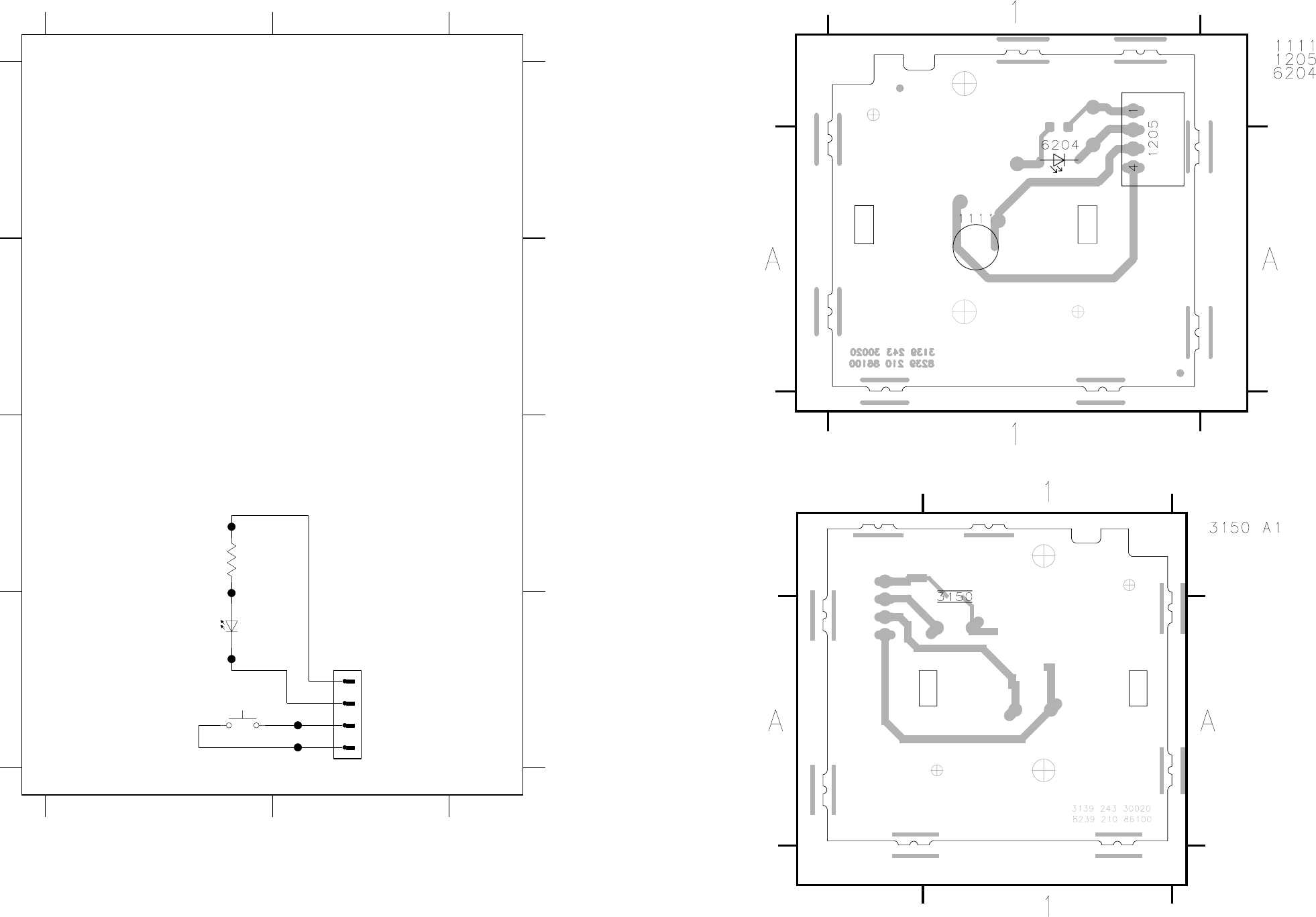
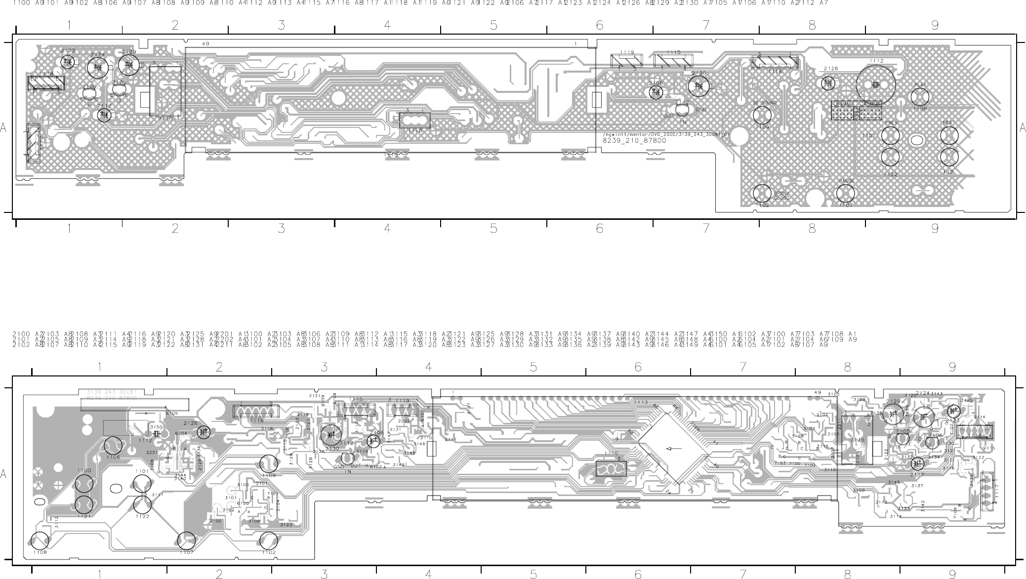
12. SCHEMATIC DIAGRAM AND PARTS LOCATION
1111 D1
1205 D2
3150 C1
6204 D1
T134 C1
T135 D1
T136 D1
T137 D2
T138 D2
1
2
3
4
GEEN SYMBOOL
CQW10
STANDBY
D1: Standby PCB (N1B)
To Con 1117 of Display PCB
12
12
A
B
C
D
A
B
C
D
SKQNAB
1111
1205 EH-S
T134
LTL-1CHPE
6204
3150
100R
T137
T138
T136
T135
Volume / Standby PWB
23 24
Display
8-Bit A/D
Converter
Counter
VFT driver circuit (automatic display)
80k pull
down
8-Bit h.break. v.
out w. latch P8
8-Bit high breakdown voltage
output part ewith latch P7
8-Bit high breakdown v.
output port with latch P6
4-Bit In/Output
sink open drain
out. port w. latch P9
5-Bit h. breakd. v.
out w. latch PD
8-Bit Input/Output
(tri-state) P0 3-Bit In/Output
with latch P2
8-Bit Input/Output
(tri-state) P0
3-B. I/O P3
sink o.drain
RAM ROM
Program
CPU
V24
V25
V26
V27
V28
V29
V30
V31
V32
V33
80k pull down 80k pull down
P6-P9 source open drain 80k pull down
source open
drain 80k p.d.
VDD
VAREF
VASS
AIN13
AIN12
AIN11
AIN10
AIN7
AIN6
AIN5
AIN4
AIN3
AIN2
AIN1
AIN0
SCK0
V7
V6
V5
V4
V3
V2
V1
V0
SO1
P03
(tri-state) P5
8-Bit Input/Output
(tri-state) P4
8-Bit h. breakdown v.
XIN
-RESET
XTOUT
XTIN
TEST
-STOP
-INT0
-INT1
TC2
-DV0
TC4
TC1
INT2
INT4
SCL
SCA
P04
P05
P06
P07
VSS
XOUT
V34
V35
V36
VKK
-SCK1
SI1
V23
V22
V21
V20
V19
V18
V17
V16
V15
V14
V13
V12
V11
V10
V9
V8
VCD
D
SHUFFLE
CHAPTER TRACK
SCAN A-B
FTS TOTAL TRACK
TRACKTITLE
TIME
CHAPTER
VD
TITLE
WREPEAT
L
DIGITAL
SURROUND
L
R
CR
SSS
A1 : FRONT DISPLAY PCB
TMP87CH74
7104
11 12 19
VFD GRID14
PLAY
65
PAUSE
to scart
54 46
53
MICRO-
P50
5056 49
17
TO 1205
F127
For DVD732 only
scart PIN 10
INFO : FIL2-FIL1=4.8Vac-RMS
MICRO+
38
30
29
28
27
26
25
42
F126
41
F128
STOP
F116
+5V stb
F117
OPEN / CLOSE
3D SOUND
OPTION
4
PREVNEXT
89 2216 21
39
80
79
STBY - LEDCONTROL
37
36
35
OPTION
7
-40V
1
STBY control
10
VFD GRID 12
34
23 13
5152
63 62 61
70
69
71
72
73
55
75
P50
interface
68
67
(-40V)
33
32
31
10 11 12 13 14
123456
45 44 4348 47
40
OPTION
F118
+12V
GND
20
SCL
SCA
64
66
For DVD 751
only
76
77
5614 15
59
60
24
78
23
VFD GRID 13
18
P50
74
58
123456789
7 8 9 10111213 14
A
B
For models with P50 only
D
E
F
G
H
I
57
C
6789333435363738394041424344454849 5212223242526272829303132
1113 110111213141516171819 220
F204
14-MT-26GNK
F165
F166
2107
33n
F217
F168
3134
330R
27K
3101
F120
3118
10K
F129
F161
F216
F119
F181
2211
BAS216
6100
3107
0R
100p
F121
10K
3140
2128
1n
22u
2130
3100
22K
2119
22p
3145
10K
F153
VKK
2114
22p
3109
SKQNAB
1101
4K7
3126
10R
10R
3128
F164
3138
470R
3105
0R
2131
1n
+5Vstb
2202
1n
+5Vstb
22p
2121
F202
10R
3133
F212
1110
VKK
6101
BZX284-C8V2
3114
10R
3120
470R
2110
33n
F211
F149
VKK
F229 F147
F228
1115
EH-B
1
2
3
4
F232
F187 SKQNAB
1109
22p
2118
F141
33n
2108
SKQNAB
3104
1100
3131
4R7
100K
F104
F137
2201
F179
3113
4K7
33n
2125
22p
10K
3143
4K7
3139
BC847B
7108
F203
2105
33n
1108
SKQNAB
1107
SKQNAB
220p
2100
3106
220R
2101
220p
F178
F107
F177
7112
MC79L24
GND
3
IN
2
OUT
1
F219
3119
10K
3144
100K
2111
33n
6104
BAS216
VFIL_DC
VFIL_DC
2106
10u
1102
SKQNAB
F201
F180
F150
F244
F245
F183
+5Vstb
VKK
82K
3108
4K7
3110
F241
F243 10R
F242
F200
3122
7109
BC857B
F109
F108
BAS216
6105
3150
4K7
F176
F227 F175
F167
F230
F138
F139
3130
10R
F171
BC327-25
7106
F170
F173
F102
F103
F234
F223
F235
F213
F124
F210
F209
F133
F208
82K
3103
7102
BC847B
10K
3123
7100
BC847B
VKK
+5Vstb
+5Vstby
+12V
F105
1202
1207
3147
10K10K
3146
SKQNAB
1106
2116
33n 10u
2117
2109
VKK
F130
33n
GND
1
OUT
3
VS
2
2115
22p
4K7
3115
7110
TSOP1736
F163
3102
47K
F159
F157
F160
F155
F152
F169
+5Vstb
2
3
100R
3148
100R
3149
1
2
3
4
5
EH-B
1119
1
3121
4K7
EH-B 1116
F123
F122
F132
2129
7107
BC847B
2123
10u
22u
F101
4R7
3117
F100
22u
10R
3127
2124
BC337-25
7105
3112
4K7
F106
3111
4K7
F113
F135
+5Vstby
F114
F221
22p
2120
F222
3132
330R
+12V
F214
PKM13EPY
1112
3136
F218
33n
2122
1K
PH-B
1118
1
2
3
4
5
10R
3129
7101
BC847B
F231 100p
2103
F131
330R
F186
10K
3137
3142
BC847B
BZX284-C10
6102
F151
7103
F154
4
3135
220R
F184
F205
1117
EH-B
1
2
3
F206
F207
F172
F158
F156
3116
82K
10u
2126
3125
10R
F142
F140
F162
F233
F226
1122
SKQNAB
2102
100p
SKQNAB
1121
7202
F125
STBKEY+ STBKEY-
+5Vstb
V15
G14
G13
G12
OUT_P50 IN_P50
V13V14
V15
V14
IN_P50
OUT_P50
STBKEY+
STBKEY-
K_DATA
K_RESET
K_CLK
K_STROBE
FIL1
FIL2
FIL1FIL2
V13
25 26
Display PWB
27 28
Supply and video switching (/N1B)
F276 E4
F277 F2
F278 F2
F279 F3
F280 F2
F281 G1
F401 C14
F500 G11
F501 G12
F502 H11
F503 I12
U182 B6
U183 B8
U185 D13
U228 H2
U229 G3
U230 H2
U275 I2
7901-B G8
7901-C H8
7902-A F10
7902-B G10
7904-A B8
7904-B C8
7904-C D8
7905-A B10
7943 I2
7945 F11
7946 H11
F109 A2
F110 A2
F112 B2
F113 B2
F120 B13
F121 B14
F130 D2
F135 E2
F138 D2
F142 D2
F144 D2
3624 F2
3625 G1
3626 B3
3627 E3
F150 E2
F211 B11
F260 B2
F269 B3
3723 I2
3762 D13
3769 G12
3770 G11
F270 B4
F271 B3
F272 C3
3774 H11
3804 G11
3805 G12
F273 C2
F274 C2
F275 E3
7304 B13
7331 B3
7332 C3
7333 F3
7334 F3
7335 G2
7400 C13
7900-A F6
7900-B G6
7900-C H6
7901-A F8
RGB switching
D
E
F
7902-C H10
7903-A B6
7903-B C6
7903-C D6
B
C
D
E
7905-B C10
7905-C D10
7935 H3
I
1300-1 A1
1300-2 A1
7947 I12
7949 G12
F106 A2
1300-8 B1
1300-9 B1
1301-10 D1
1301-13 D1
1301-14 D1
1301-15 E1
1301-16 E1
1301-2 D1
1301-8 D1
1301-9 E1
2354 B13
VIDEO SWITCHING
123
3695 H2
3696 G3
3720 H2
3722 H2
8 9 10 11
3771 H11
3772 I11
3773 I12
123
6302 C2
6403 C1
6404 D13
7 8 9 1011121314
A
B
C
BLANKING
CVBS SWITCHING
supply
2384 B11
G
H
I
A
2412 B14
2452 C13
2453 C14
2524 B6
F
G
H
2525 B9
2527 A6
2528 A8
1300-3 A1
1300-5 A1
1300-6 B1
2529 A10
2530 C6
2531 C8
2532 F6
2533 G6
2534 C10
2535 F8
2536 F10
2537 G8
2541 B14
2545 C4
3433 B14
3615 B3
3616 B3
3617 C2
3618 C3
3619 C2
3620 E3
3621 F2
3622 F2
3623 F3
4567
SUPPLY &
12 13 14
456
F113
E
6
S
10
Vdd
16
Vee
7
Vss
8
Y0
2
Y1
1
Z
15
F276
HEF4053BT
7903-B
+6V
-5V
10
3695
10K
1301-10
1301-16
16
L78L33
7400
2
13
+6V
F272
3626
0R
Vdd
16
Vee
7
Vss
8
Y0
12
Y1
13
Z
14
F271
+6V
HEF4053BT
7902-A
E
6
S
11
U228
U229 7902-B
HEF4053BT
6
E
10
S
16
Vdd
7
Vee
8
Vss
2
Y0
1
Y1
15
Z
1301-2
2
7943
BC847B
10K
3622
F260
+8VAud
3773
10K
6
E
10
S
16
Vdd
7
Vee
8
Vss
2
Y0
1
Y1
15
Z
BAS216
6302 7904-B
HEF4053BT
7332
BC857B
F278
F279
F121
56K
3720
2
GND
1IN 3
OUT
+12Vstby
7905-A
HEF4053BT
6
E
11
S
16
Vdd
7
Vee
8
Vss
12
Y0
13
Y1
14
Z
LF80C
7304
1300-9
9
1300-6
6
1300-8
8
1300-3
3
1300-5
5
100n
1301-9
9
3433
0R
2541
U182
F138
22n
25282527
22n
22n
2536
47K
3770
47u
+12Vstby
2453
F273
F503
F274
F269 F270
3V3
-8Vstby
4R7
3615
+12Vstby
3618
1K
10K
3619
10K
3617
2534
22n
7331
BC547B
+6V
220n
2384
E
6
S
10
Vdd
16
Vee
7
Vss
8
Y0
2
Y1
1
Z
15
F281
HEF4053BT
7905-B
22n
2530
BC847B
7935
F130
1300-2
2
6404
BZX284-C5V1
270R
3762
E
6
S
9
Vdd
16
Vee
7
Vss
8
Y0
5
Y1
3
Z
4
U185
HEF4053BT
7905-C
14 U183
HEF4053BT
7904-A
E
6
S
11
Vdd
16
Vee
7
Vss
8
Y0
12
Y1
13
Z
3805
10K
F502
BC847B
7334
14
F501
F500
1301-14
+12Vstby
4K7
3616
BC327-25
F135 F275
7333
3696
10K
+6V
3627
0R
Vdd
16
Vee
7
Vss
8
Y0
5
Y1
3
Z
4
+6V
HEF4053BT
7902-C
E
6
S
9
F280
3621
4K7
F142
E
6
S
9
Vdd
16
Vee
7
Vss
8
Y0
5
Y1
3
Z
4
+8VAud
HEF4053BT
7903-C
220n
2524
3769
47K
+12Vstby
+8Vstby
1K
3625
1301-15
15
+12Vstby
BC847B
7949
F120
56K
2531
22n
+6V
3723
10K
3624
U275
+6V F401
Z
4
7900-C
HEF4053BT
E
6
S
9
Vdd
16
Vee
7
Vss
8
Y0
5
Y1
3
7946
BC857B
BC847B
7947
3772
47K
3774
47K47K
3771
BC857B
7945
+12V
7900-A
HEF4053BT
E
6
S
11
Vdd
16
Vee
7
Vss
8
Y0
12
Y1
13
Z
14
Vdd
7
Vee
8
Vss
12
Y0
13
Y1
14
Z
1300-1
1
7903-A
HEF4053BT
6
E
11
S
16
3623
4K7
7335
BC847B
+6V
-8Vstby
+12Vstby
22n
2533
22n
2535
22n
2532
47K
3804
+12Vstby
U230
8
1301-8
S
16
Vdd
7
Vee
8
Vss
5
Y0
3
Y1
4
Z
2452
220n
Vee
7
Vss
8
Y0
2
Y1
1
Z
15
HEF4053BT
7901-C
6
E
9
7
Vee
8
Vss
12
Y0
13
Y1
14
Z
7901-B
HEF4053BT
E
6
S
10
Vdd
16
HEF4053BT
7901-A
6
E
11
S
16
Vdd
47u
2412
2545
47u
+6V
2525
220n
7904-C
HEF4053BT
6
E
9
S
16
Vdd
7
Vee
8
Vss
5
Y0
3
Y1
4
Z
220n
2354
4R7
3620
+6V +6V
BAS216
+6V +6V
+6V
6403
13
F211
2529
22n
1301-13
56K
3722
F277
+5V
7900-B
6
E
10
S
16
Vdd
7
Vee
8
Vss
2
Y0
1
Y1
15
Z
HEF4053BT
+6V
22n
2537
DC_OFF
YCVBSOUT_AUX
-5V
-5V
-5V
-5V
-5V
-5V
YCVBSIN_TV
CVBS
SELECT
YCVBSIN_AUX
YCVBSOUT_TV
CVBS
SELECT
0|6|12
FBIN_AUX
SLB_AUX
B
G
R
CVBS
0|6|12
RCOUT_TV
-5V
-5V
-5V
-5V
-5V
-5V
-5V
-5V -5V
SELECT_HIGH
SELECT_HIGH
G
SELECT
GOUT_TV
GIN_AUX
B
SELECT
BC_TV
BC_AUX
SELECT
SDA
SCL
R
Y_ENC
DC_OFF
SELECT
C_ENC
FBOUT_TV
SLB_TV
0|6|12
RCIN_AUX
-9.5V
-9.2V
-8.6V
-0.6V
0V
-1.2V
0V
+11.5V
+11.2V
+10.8V
0V
0.7V
0V
+6V
0V
0.7V
0.7V
0V
11.4V 8V
8V 3.3V
-5.2V
SELECT:
0V DURING PLAYER SCRIPT: "SCART DVD"
6V DURING PLAYER SCRIPT: "SCART LOOP"
SELECT HIGH:
0V DURING PLAYER SCRIPT: "SCART DVD"
12V DURING PLAYER SCRIPT: "SCART LOOP"
ALL DC VOLTAGES MEASURED
IN STOP MODE.
TP1
TP2
TP3
TP4
TP5
TP6
29 30
Audio A/V MUX (/N1B)
NC
NC
DECODER
BUS
SUPPLY
DRIVER
CONTROL
INTERFACE
DAC’S
VOL/MUTE/DEEMPH
INTERPOL FILTER
NOISE SHAPER
NC
DIGITAL
INTERFACE
U191 E3
U226 C12
U227 D7
F267 H8
F268 G7
F400 A9
F406 B8
F408 B5
F410 B7
F414 A2
F415 D5
F416 D8
F421 D6
F422 B1
F423 D7
F424 E8
F425 B1
F432 C1
F437 D3
F448 G1
F455 G1
F478 I1
F486 H11
F487 H11
F488 H12
F489 H13
3765 H6
3766 C3
3767 C4
F490 H12
F497 E1
F504 E1
5400 H11
6400 H14
6401 C11
F505 G2
U186 C12
U187 B7
7402 A4
7403-A B6
7403-B D6
U188 C3
U189 C3
U190 E3
7405 E8
7406 C8
7407 B8
7917 B12
7944 G7
7948 C4
F139 C13
F141 C13
F176 D12
F177 B12
F180 A12
F181 D12
F265 G8
F266 H7
3445 D9
3446 D7
3447 E7
F403 B5
F404 B6
F405 B8
3454 A5
3455 B5
3456 B7
F411 C8
F412 A4
F413 E9
3462 B7
3463 C8
3464 B6
F417 D8
F418 D5
F419 B1
3511 C1
3512 C2
3517 C7
3519 A3
3610 F8
3611 G7
3612 H7
3613 G7
3614 H8
3631 D7
3632 C6
3634 A4
3635 B11
3764 H6
2373 A12
2450 C6
2455 D4
3768 G7
3802 E1
3803 G2
2459 A5
2460 A2
2461 E6
7329 G8
7330 H8
7401 B2
2469 D2
2471 D3
2472 D3
7403-C A9
7403-D E9
7404 D8
2497 C11
2498 C11
2519 I13
2542 H7
2543 H10
2544 H11
3321 C14
3322 C14
3338 E13
3339 E12
3340 A12
3341 A13
3442 D8
3444 D4
AUDIO SCART SWITCHING
Option L/R
1300-10 G1
3448 D5
3451 E5
3453 E6
1300-14 G1
1300-15 H1
1300-16 H1
3457 B8
3459 B5
3461 B9
1300-20 I1
1300-21 I1
1300-22 I1
3505 H10
3507 H10
3508 H12
1301-11 E1
1301-12 F1
1301-3 D1
1301-4 D1
1301-5 E1
1301-6 E1
1301-7 E1
1402-B D10
1402-C C10
1405 I14
1410 D14
2360 C14
2361 C13
2372 D12
123
2456 D6
2457 D9
2458 D6
789
2462 B6
2463 B9
2464 C6
13 14
1
2488 H14
2495 I13
2496 C11
4567891011121314
A
B
C
D
E
F
1300-11 G1
1300-12 G1
1300-13 G1
G
H
I
1300-17 H1
1300-18 H1
1300-19 I1
A
B
C
1300-4 F1
1300-7 F1
1301-1 D1
D
E
F
G
H
I
456 101112
AUDIO
23
U227
F176
U187
3632
100R
3634
2K2
3519
5K6
100R
3631
10K
100U
2456
3444
10K
3451
3453
F432
10K
F422
F425
F412
F419
12
13
14
4
11
F414
3613
2K7
MC33079
7403-D
BC817-25
7402
3611
4K7
F423
F415
F418
-8Vstby
F411
F405
F410
F406
F400
F408
F404
F478
2463
10K
3461
24573445
10K
1n
1n
3511
10K
10K
3512
BC817-40
7404
7406
2472
47u
BC817-40
100n
2471
100R
3457
2K7
3463
3447
2K7
100R
3517
6
5
STEREO_R
STEREO_L
YKC21-3930
1402-B
4
3
YKC21-3930
1402-C
+5V
12
F177
BC847B
7329
F141
52030
1300-12
F139
F416
F437
F424
F417
F413
F421
2360
50
2373
4u7
47p
100R
3322
47p
2361
1K
3339
3321
100R
F403
2372
50
4u7
3767
22K
3V3
22K
3766
U191
7948
BC857B
U189
U190
F505
-8Vstby
4R7
3803
F448
F455
2464
+5V
100p
2461
100p
100p
2455
100p
2459
7405
BC817-40
BC817-40
7407
2496
22n
3635
220R
6401
BZX284-C9V1
100u
2498
100R
3442
2497
22u
23
R4
20
R5
19
RO1 12
RO2 14
RO3 16
RO4 18
SCL 27
SDA 28VS3
L1
4
L2
5
L3
6
L4
9
L5
10
LO1 11
LO2 13
LO3 15
LO4 17
78
2122
R1
25
R2
24
R3
1300-15
52030 15
TEA6420
7917
ADDR 26
C2
GND1
1300-13
52030 13
52030
1300-14
14
1300-11
52030 11
52030
1300-18
18
7
52030
1300-10
10
F504
52030
1300-7
1300-4
52030 4
F180
100n
2488
2
34
6
78
3505
100R
+5V
5400
7CHA
1
100n
2495
68R
3508
6400
GP1F32T
3
1
2
F489
F490
2519
100n
2u2
2542
7
47K
3768
1410 EH-B
1
2
3
4
5
6
+8VAud
7330
BC847B
+12V
F488
52030
1300-22
22
2543
47p
2544
10u
3765
10K
21
10K
3764
BC847B
7944
52030
1300-20
20
1300-21
52030
17
1300-19
52030 19
52030
1300-16
16
1300-17
52030
U186
U226
3341
47K
3338
47K
3340
+8VAud
F181
1K
F497
1301-6
52030 6
1301-7
52030 7
52030
1301-5
5
F265
100R
3507
F266
F268
F267
+6V
3455
10K
3610
4K7
3614
22K
52030
1301-3
3
3612
47K
52030
1301-12
12
1301-1
52030 1
1301-11
52030 11
+6V
4R7
3802
2K7
3446
3V3
3448
10K
3V3
2469
22n
+12Vstby
2460
22n
1
3
2
F486
YKC21-3416
1405
VO1P
31VO2N
32VO2P
1VO3 2VO4
4VO5 5VO6
30
VREFA
3
VSSA
20
VSSD
11 WS
3V3
DS
18L3CLK
19L3DATA
17L3MODE
23MUTE
7
8
15
9STATIC
16 SYSCLK
27 TST1
22TST2
6
VDDA
21
VDDD
29 VO1N
28
7
4
11
7401
UDA1328T
10 BCK
25DEEM0
24DEEM112 DI12
13 DI34
14 DI56
26
2458
7403-B
MC33079
5
6
22n
+8VAud
22n
2450
11
7403-C
MC33079
10
9
8
4
11
+8VAud
MC33079
7403-A
3
2
1
4
-8Vstby
+8VAud
1301-4
52030 4
3456
-8Vstby
-8Vstby
2462
100U 100R
10K
3459
10K
3464
3462
3454
10K
F487
2K7
HP_L HP_L
HP_R HP_R
{PCM_OUT0,PCM_OUT1,PCM_OUT2,SCLK,LRCLK,PCM_CLK,DEEM0,DEEM1}
DIG_OUTSTANDBY
KILL
STANDBY
DIG_OUT
HP_L
HP_R
SCL
LIN_TV
LOUT_TV
LIN_AUX
LOUT_AUX
ROUT_TV
ROUT_AUX
RIN_AUX
RIN_TV
SDA
DC_OFF
KILL
KILL
KILL
KILL
KILL
KILL
TP7
TP8
TP9
TP10
TP11
TP12
TP13
TP14
TP15
TP16
TP17
TP18
KILL:
-8V DURING PLAY
+4.8V DURING STOP, NEXT, PREVIOUS
+1.6V
0V
6V
0.6V
0.7V
0V
9.2V
4.6V
TP12
TP12
TP12
TP13
TP14
TP15
TP15
TP15
31 32
Scart panel (N1B)
2383 B3
2385 C3
2395 C5
2402 F5
2404 E5
2408 F5
2409 I5
C
2509 C8
2511 H8
2521 B12
2522 A5
2523 B5
TV-SCART
AUX-SCART
1 10 11 12 13
12
3349 A5
3351 B4
3359 B5
3363 B4
3366 B5
3394 C4
3397 C5
43 11 12 13
A
B
C
D
3638 D9
3639 E9
3640 E8
3641 F8
3642 C8
1304-1 C13
1304-2 C6
1304-3 G13
E
F
G
H
I
A
B
SCART
3675 C11
3676 G10
3677 H11
3678 G3
3679 G3
3680 D10
3681 D10
2499 G5
D
E
F
G
H
I
2507 D9
2508 F8
3692 D4
3693 E4
3694 I4
3697 G4
3698 E11
3313 D12
3314 A11
3315 A11
23456789
3725 F9
3726 E9
3727 G3
3731 C9
3732 I9
3733 H9
3734 F8
3407 E5
5678910
3636 G2
3637 G2
3756 D9
3757 F8
3758 H8
3800 G9
3801 G10
3643 D8
3646 H8
3647 I8
2353 A10
2355 A10
2357 B10
2358 A12
2359 B10
2371 I11
2378 A3
2382 A3
7929 C10
7930 C8
7931 G9
7933 H10
7934 H9
7936 G3
7937 D10
3682 F9
2500 E12
2501 F11
2502 C11
2503 G11
2504 H11
2506 G2
3690 I11
3691 C4
F134 C13
F137 C13
F140 C13
F145 D13
F148 D12
3699 F10
3700 C10
3701 G10
3316 A12
3318 B11
3319 B11
3320 B12
3323 B11
3325 B11
3343 I11
3348 A4
F234 D6
F247 E6
F259 F6
U131 G3
U132 E10
U133 F10
U134 C9
3735 F9
3408 F4
3409 D4
3413 D4
3425 F5
3432 I4
3629 C5
3748 C8
3749 G2
U145 D10
U146 D9
U147 E9
U148 E13
U149 F11
7918 I10
7919 C3
7920 D3
3648 G2
3649 D9
3650 E8
3651 C8
3653 H9
3672 G5
3673 E11
3674 F11
U161 C8
U162 G10
U163 G9
U167 H11
U168 H10
U169 H9
U170 H9
7938 F10
3683 F10
3684 C9
3685 C10
3687 G9
3688 H9
3689 H10
F127 B11
F133 B11
U201 E4
U202 E2
U203 F2
U204 E6
U205 G2
F149 D13
F183 F13
F193 A4
3702 I10
3703 I10
3704 D3
3705 E3
3706 F3
3707 I3
3721 G10
3724 H9
U213 F8
U214 F8
U215 D9
U216 D8
U217 C8
U218 C8
U219 B8
U136 F6
3736 E9
3737 E10
3738 H2
3739 G3
3744 D8
3747 C9
U143 E11
U144 D11
U222 G2
U223 A8
U225 D6
U278 G8
U279 G9
U150 F10
U151 F9
U152 F9
7921 E3
7922 I3
7923 G4
7924 G2
7925 D11
7926 D9
7927 F10
7928 F9
U159 C9
U160 C9
U184 H8
U193 A2
U194 B2
U195 B2
U196 C2
U197 C2
7939 C9
7941 H9
7942 G10
F103 H10
F114 A11
F115 A11
U199 D4
U200 C4
U198 D2
U206 I4
U207 I2
U208 I8
U209 I10
U210 H8
U211 H8
U212 G10
F195 B4
F205 B4
F212 C4
F216 C6
F218 D6
F219 C6
F222 C6
F229 D6
330R
+8Vstby
U137 G4
U138 G4
U139 G3
U140 G2
U141 G2
U142 D13
U220 B8
U221 A8
U153 F8
U154 D13
U155 E13
U156 F13
U157 C10
U158 C10
100R
3689
3653
100R
3688 7941
BC857B
BC847B
7934
2509
2u2
3677
75R
BC847B
7933
3702
1K
U162
U163
U155
U193
2503
220p
100K
3647
U225
100K
3641 100K
3643
100K
3639
7928
BC847B
100K
3646
BC857B
7938
3638
100K
3640 100K
3642
100K
3721
150R
2501
220p
2523
+8Vstby
+8Vstby
220p
100R
330R
3650
3682
100R 3683
U136
1K
3699
75R
3674
+8Vstby
7927
BC847B
+8Vstby
330R
3732
2507
2u2
U223
U220
U221
+8Vstby
U219
U216
U214
U215
U212
U213
U210
U211
+8Vstby
U209
3673
75R
BC847B
7925
3698
1K
3704
6K8
+8Vstby
7919
BC847B
U159
U160
U161 U134
U157
U158
U154
330R
3736
22R
3726
330R
37353725
22R
100K
3636
100K
3637
100K
3758
100K
3749
3756
100K
3757 100K
3748
100K
330R
3739
U141 3727
22R
U140
U131
U139
F137
U137
U138
F115
+8Vstby
+8Vstby
220p
2499
330R
3648
3678
100R 3679
100R
7924
BC847B
BC857B
7936
U218
U217
U279
4K7
3800
U278
+6V
4K7
3801
3705
7920
BC847B
6K8
1K
3692
75R
3432
1K
3691
3409
220R
6K8
3703
3690
7918
BC847B
75R
1K
7942
BC857B
3629
U206
470R
3701
U205
U204
U222
U202
U203
U200
U201
U199
3731
22R
U198
3744
330R
F149
3737
330R
F145
F148
F133
50
2357
F140
F127
1K
3319
4u7
F114
F134
220p
220p
2409
3738
330R
2408
220p
330R
3747
+8Vstby
2521
U184
2511
2u2
U169
U170
U168
F103
U167
3733
330R
3734
330R
22R
3724
75R
3425
3413
47K75R
3408
75R
3407
50
2385
47K
3397
3394
470R
4u7
U208
3676
150R
+8Vstby
U207
BC847B
7931
2u2
2508
+8Vstby
U153 U133
U151
U152
U196
U197
U195
3325
47K
U194
2359
4u7
50
3323
470R
47K
3320
2522
220p
U145
U144
U132
U142
U143
+8Vstby
2500
220p
3649
330R
+8Vstby
U156
47K
+8Vstby
2504
220p
4u7
2383
50 3366
3318
47K
470R
3315
4u7
2355
50
47K
3316
3314
1K
4u7
2353
50
16B
17B
18B
19B
2B
20B
21B
3B
4B
5B
6B
7B
8B
9B
1304-2
1B
10B
11B
12B
13B
14B
15B 15A
16A
17A
18A
19A
2A
20A
21A
3A
4A
5A
6A
7A
8A
9A
1304-1
1A
10A
11A
12A
13A
14A
4K7
3687
3685
3651
330R
+8Vstby
100R
3684
100R
BC847B
7930
+8Vstby
7939
BC857B
3675
75R
U150
3700
1K
U148
U149
2402
220p
220R
3313
U146
U147
75R
3672
1K
3697
7923
BC847B
7922
BC847B
6K8
3707
1K
3694
100R
3681
100R
3680 7937
BC857B
BC847B
7926
3363
1K
2382
4u7
50 47K
3359
470R
3351
50
4u7
2378
47K
3349
1K
3348
F193
F219
F183
F216
+8Vstby
2502
220p
1304-3
0350808190
MT1 MT2
F247
F259
F212
F229
F234
F218
F205
F195
F222
+8Vstby
BC847B
7929
2u2
2506
220p
+8Vstby
2395
220p
2404
2371
220p
220p
2358
6K8
3343
75R
7921
3706
3693
1K
BC847B
-8Vstby
SLB_TV
+8Vstby
-8Vstby
+8Vstby
-8Vstby
+8Vstby
-8Vstby
+8Vstby
-8Vstby
+8Vstby
{ROUT_AUX,RIN_AUX,LOUT_AUX,LIN_AUX,BC_AUX,SLB_AUX,GIN_AUX,RCIN_AUX,FBIN_AUX,YCVBSOUT_AUX,YCVBSIN_AUX}
2.2V
7.4V 7.4V
1.6V
2.6V
2.6V
2V
2.2V
7.4V 7.4V
1.6V
2.6V
2.6V
2V
2.2V
7.4V 7.4V
1.6V
2.6V
2.6V
2V
2.2V
7.4V
7.4V
1.6V
2.6V
2.6V
2V
2.2V
7.4V 7.4V
1.6V
2.6V
2.6V
2V
-0.6V
-0.6V
-0.6V
-0.6V
-0.6V
33 34
CVBS / YC panel (/N1B)
I221 H6
I241 D7
I242 D6
I245 D7
I246 D8
I247 D8
I251 D6
U130 B7
U192 G9
U224 G9
U276 B6
U277 D6
3750 B6
3751 A6
3752 B6
3759 H6
3760 G6
3761 G6
7006 F6
7007 F6
7010 H6
7011 H8
7012 D7
7013 D6
7014 D8
7300 B7
7301 B6
7310 B8
F100 B6
F101 B7
F104 B8
F107 B6
F108 B9
F600 H6
I189 F7
I191 F6
I196 F6
2538 B5
2539 D6
2540 H6
I200 G5
I208 F9
I210 G7
3040 F5
3041 F7
3043 G6
I211 G6
I214 H7
3046 H7
3049 G9
I215 H8
I219 H8
3058 D6
3059 D7
3062 D9
3063 E8
3300 B6
3301 B6
3345 B8
3347 B8
3728 D6
3729 H6
3730 B6
3740 E6
3741 D7
3742 H6
3743 H7
3745 B7
3746 B6
Y/C OUT
9
3753 D6
3754 E6
3755 D6
13 14
A
3763 B7
3999 I1
D
E
7008 F6
7009 G7
H
I
A
B
C
D
E
F
G
H
I
1303 F10
1402-A B9
2032 H8
2377 B9
2505 G9
2520 G9
123
3036 F7
3038 F6
3039 F5
456
3044 F5
3045 G6
78
3050 H8
3056 D6
9 1011121314
12345678 101112
CVBS & YC
B
C
F
G
I208
75R
3049
470n
2032
+5V +5V
I245
3041
8K2
3036
2K2
-5V
22K
7006
BC847B
+8Vstby
3038
+8Vstby
I246
I251
U130
F101
I219
I221
1402-A
2
1
YKC21-3930
+8Vstby
+8Vstby
I196
3301
100R
330R
3300
7301
BC847B
BC857B
7300
1K
3347
75R
3345
7310
BC847B
2505
220p
330R
3743
I241
I211
3742
330R
I242
3760
100K
+8Vstby
220R
3050
I210
I247
I215
+8Vstby +8Vstby
I214
330R
3043
100R
3045
I189
+8Vstby
1K
3063
100R BC847B
7014
+8Vstby +8Vstby
3059
7013
BC857B
7012
100R
3058
BC847B
3056
330R
1303
TCS79
5
6
7
1
3
4
2
7007
BC847B
3729
22R
3039
F600
47K
3040
27K
3759
100K
F107
F100
F104
2540
2u2
F108
220p
2377
330R
3740
100K
3754
+8Vstby
100K
3753
3763
2u2
2539
3745
330R
100R
3746
22R
3730
3752
100K
330R
U276
+8Vstby
3751
100K
3750
100K3761
100K
2538
2u2
3044
22K BC847B
7008
2520
BC847B
7011
220p
3046
100R
BC857B
7009
3741
330R
7010
BC847B
22R
3728
100K
3755
3062
75R
CVBS
0|6|12
U277
Y_ENC
C_ENC
TP19
TP20
TP21
2.2V
7.4V 7.4V
1.6V
2.6V
2.6V
2V
2.2V7.4V
7.4V
1.6V 2.6V
2.6V
2V
2.2V 7.4V 7.4V
1.6V 2.6V
2.6V
2V
0.6V
0.6V
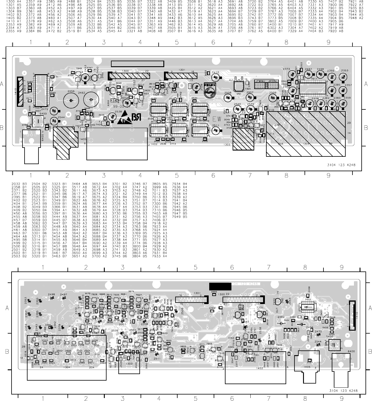
35 36
A/V Mux panel (/N1B)
_Z
_A
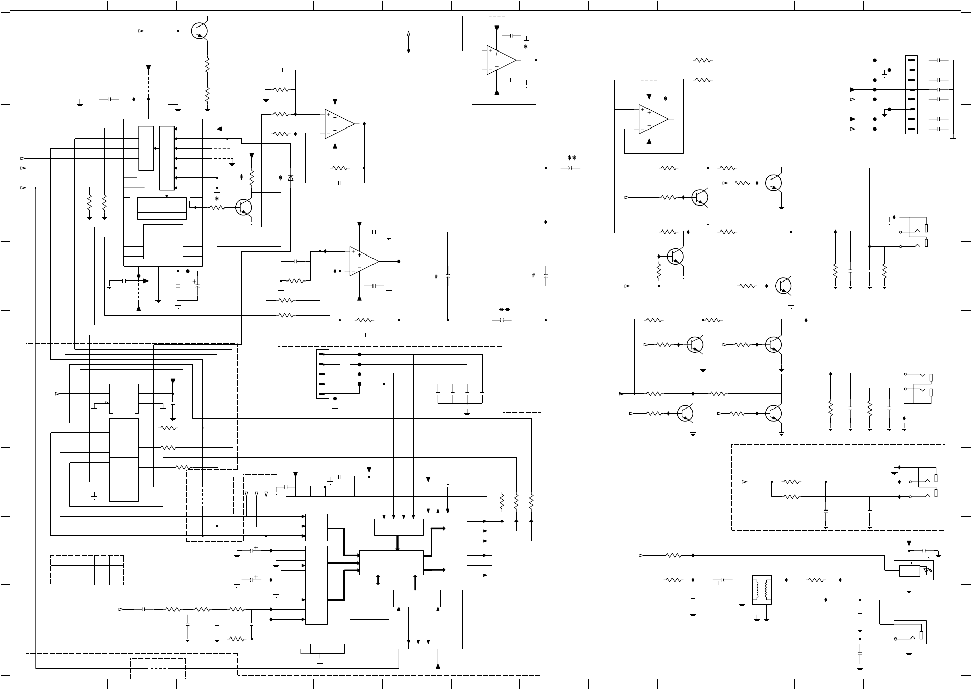
37 38
A/V board (A1B, /S1G, /U1B)
DRAM
MICOM uF
DSP
IN DIGITAL
OUT
IN
MIC
IN
TIMING GENE.
OUT
ANALOG
ANALOG
DIGITAL
CONTROL
INTERFACE
DAC’S
VOL/MUTE/DEEMPH
INTERPOL FILTER
NOISE SHAPER
NC
DIGITAL
INTERFACE
EN
G1
1
MUX1~
DRIVER
7007
BC817-25
C1: AV PCB
10
7404-A A7
7404-B C9
7405 E2
7406 H13
F500 E5
F501 E5
F502 E5
3435 C3
Y3
*
I407 D5
I406 B8
Y1
3432 I3
3433 I3
7402-B D5
7403 G7
(3n9)
FOR DVD 741,
FOR DVD732
Y4
Y3
Y2
3436 G7
3437 G7
F547 A13
F548 A13
F549 A13
F550 B13
F551 B13
F552 B13
4418 G3
4440 I2
74HCT157D
5
313
I408 D5
I409 D6
DVD 751
G1
6
14
H
3592 C4
**
L/R No Swap
*
Reserved Parts
*
3412 B7
3413 B7
5400 H11
6411 C4
7000 A3
7001 B7
7002 B8
7003 F10
F503 F5
F504 F5
3452 E11
3453 H12
3434 I3
FOR DVD732
OPTION
3430 G3
3431 I2
Y4
L/R/Swap
#
2
ONLY FOR DVD 732
2424 F6
4400 A2
4401 D2
4402 A7
4403 B8
4414 B3
4415 B3
4416 G3
4417 G3
2436 G12
2437 G13
3438 G8
3439 D7
3440 D9
3441 F10
3442 D7
3443 D9
I400 B2
I401 B4
I402 A6
I403 B4
I404 B6
I405 B12
F545 A13
F546 A13
3402 C1
3403 C1
12 13
1234
Y1 Y2
3404 A4
3405 B4
3406 B4
3407 B5
3408 B6
3411 B6
13
A
3414 A10
3415 A10
3416 D4
3417 D4
3418 E4
3419 E5
7004 F11
7005 D8
7006 E9
7007 G10
7008 G12
7039 C3
7400 B2
7402-A B5
G
H
2407 A7
2408 A7
2409 D4
2410 E5
2411 C5
2412 D6
2425 F7
2426 F7
2428 G5
2429 H3
2430 H4
2431 I2
2434 D12
2435 D13
2422 F2
2423 F6
2438 I10
2439 H10
2440 I13
2441 I12
2442 H13
2445 D5
3444 F11
3445 G10
3446 G11
3447 G12
3448 G13
3449 H10
3450 H10
3451 E10
10 11
I432 H12
I433 I12
I434 H4
I435 I4
I436 I4
I437 I4
5 6 7 8 9 10 11 12
I532 D2
I533 D3
B
C
D
E
F
G
3420 F10
3423 F11
3424 C12
3425 C12
3426 D12
3427 D12
3428 F2
3429 F2
2405 C5
2406 B6
I410 C6
I411 B5
I412 F10
I413 B12
I414 E11
I418 F10
2413 B13
2415 C12
2416 C13
2417 A13
2418 A13
2419 A13
2420 B13
2421 B13
I430 H10
I431 H11
L
1
2447 I3
2448 I3
2449 I4
2450 G4
2507 C5
2508 C6
3400 A3
3401 A3
LEFT
RIGHT
11
I
1002 A13
1003 E4
1400 I13
I442 G7
I443 H7
I444 H8
I446 D13
I447 D13
I450 C13
I529 D13
I530 F13
1401-B B13
1401-C F13
1405 D13
2400 A2
2401 A4
2402 D2
2403 D2
2404 D3
H
I
A
B
C
D
E
F
I532
I419 G10
I421 D8
I422 D8
I423 F13
I424 D9
I425 F12
I426 G11
I429 H10
23456789
I418
+5VD
I529
2411
22n
22K
3434
F550
2437
220p
3441
100R
I431
220p
2436
-5VA
100p
BC817-25
7003
6
7
8
4
+5V
2401
2420
1n
LM833D
7404-B
5
+5VA
I533
3424
10K
4u7
2430
100R
3412
1n
2424
2K7
3446
F500
I422
F502
2418
1n
2416
1n
2
YKC21-3416
1400
1
3
I437
I403
I429
I434
3405
10K
3436
47R
I411
3416
10K
68R
3453
100u
2406
-5VA
3419
10K
2407
100R
3451
F548
F549
22n
I424 3425
10K
2434
470p
EH-B
1003
1
2
3
4
5
3414
I413
100n
2442
3420
2K7
100R
I407
I401
2429
4u7
2K7
3435
2409
100p
3452
100R
100R
3411
18
31
SDI SDO
28
TEST
41
VDA1
1
VDA2
17
VDD1
24
VDD2
42
VDL
4320
VDX
VR2
15
VRA1
4
VRA2
7
XI
21
XO
22
IFL
38 37
IFS
LI
11
LPFO1
3
LPFO2
6
LPFO3
9
LRCKI
33 30
LRCKO
LZ
12
27 26
MIC1
2
RESN
35
RI
19
RZ
5
AIR
8
AOL
14
AOR
16
BCKI
32
BCKO
29
25
CKS
EMP
39
EXTO
40
10
GNDA1
GNDA2
13
34
GNDD
GNDL
44
GNDX
23
IFD
36 TC9409BF
7403
AIL
2435
470p
+5VA
+5V
BC817-25
4403
2422
7005
2K2
3592
3V3A
22n
+5VA
LM833D
7402-B
5
6
7
8
4
10u
2439
8
4
3433
10K
LM833D
7404-A
3
2
1
2449
82p
I421
1n
2404
47u
2K7
2417
2419
1n
3413
7001
BC817-25
100R
3426
2448
4n7
3404
10K
3407
10K
10K
3406
4400
4416
+5VD
VO4
4VO5 5VO6
30
VREFA
3
VSSA
20
VSSD
11 WS
F503
7
8
15
9STATIC
16 SYSCLK
27 TST1
22TST2
6
VDDA
21
VDDD
29 VO1N
28 VO1P
31VO2N
32VO2P
1VO3 2
7400
10 BCK
25DEEM0
24DEEM112 DI12
13 DI34
14 DI56
26DS
18L3CLK
19L3DATA
17L3MODE
23MUTE
3427
100R
UDA1328T
I450
2415
1n
I406
47R
3428
3429
47R
I444
3408
2K7
I402
15
GND
8
116
VCC
+5V
74HCT157D
7405
2
34
5
67
11
10 9
14
13 12
I419
I446
3V3
4401
4418
2410
100p
+5V
4402
4440
3V3A
78
5K6
3401
5400
7CHA
1
2
34
6GP1F32T
3
1
2
YKC21-4040
1401-C
9
7
8
LM833D
7402-A
3
2
1
8
4
7406
7039
BC817-25
100n
2403
1n
YKC21-3337
1405
1
2
3
-5VA
2423
3415
3423
2K7
3448
10K
100R
I530
2428
22n
22n
2408
3449
100R
-5VA
22n
I423
2447
2400
470n
2431
3n3
3432
10K
3431
10K
I405
2K7
3445
3442
2K7
2405
3430
47R
4415
100p
F546
I443
7006
F545
100R
3440
BC817-25
3403
10K
2425
1n
2507
100u
10K
3447
4414
3439
100R
BC817-25
7004
F504
I425
6411
BAS216
47p
2441
100n
2440
3444
100R
2K7
3443
5
6
7
8
F501
1002
EH-B
1
2
3
4
I430
2413
1n
I410
BC817-25
7002
I435
1n
2421
I408
10K
3418
I426
3400
-8VHP
YKC21-4040
1401-B
6
4
5
2K2
100R
3450
100u
2508
I433
3402
10K
I432
3417
10K
I409
3V3
I442
+8VHP
I412
I414
4417
47p
2438
BC817-25
7000
22n
2402
+5VA
2412
100u
+5VD
2445
22n
3438
47R
2450
22n
F552
F547
I447
F551
I400
I404
I436
2426
22n
BC817-25
7008
Kill
KILL
ST_L
ST_L
HP_R
3437
47R
PCM_CLK
STEREO_MUTE
MICRO
PCM_OUT0
SCLK
HP_L
LRCLK
DIG_OUT
KILL
KILL
KILL
KILL
KILL
PCM_OUT2
PCM_OUT1
KILL KILL
MICRO
P50
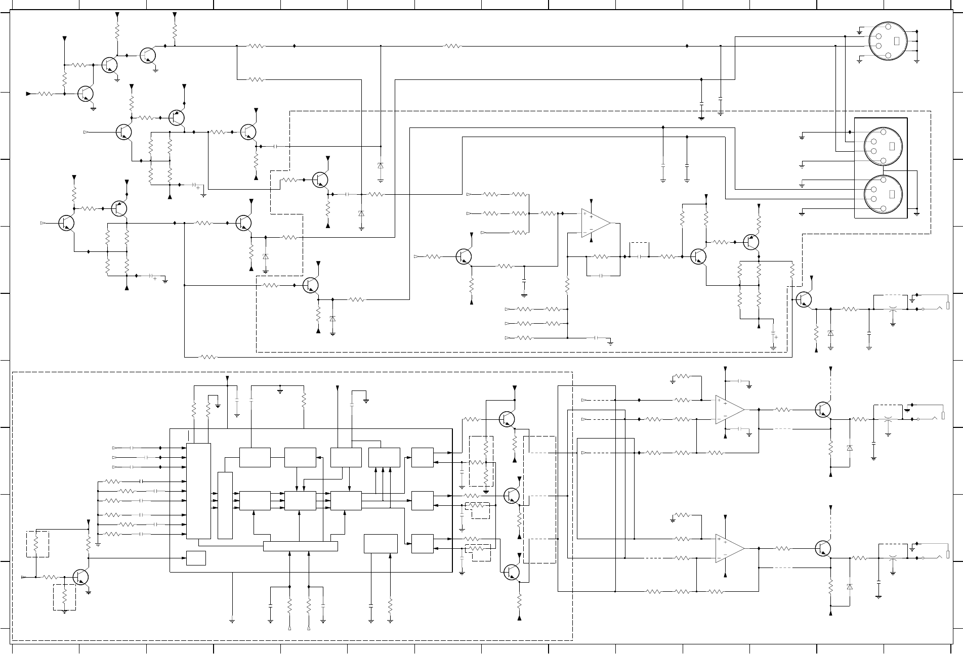
39 40
I2C
B
G
R
BUFFER
OUTPUT
OUTPUT
BUFFER
OUTPUT
BUFFER
ADJUST
LIMITING
PEAK DRIVE
LIMITING
PEAK BEAM
GAMMA
BRIGHTNESS
ADJUST
CONTRAST
ADJUST
SATURATION
LEAKAGE AND
CUT-OFF
CONTROL
BLACK
ADAPTIVE
SYNC
INPUT
SOURCE
SWITCH
Y- MATRIX
Y-CD/
4441
C2: AV PCB
*
*
F
E
D
C
2457 C10
2456 D9
3454 A1
2506 D10
2485 E9
2484 B11
2483 B11
2482 I13
2481 G13
2480 F11
2479 F11
2478 H7
2477 H7
2476 G7
1403-A D14
1402 B14
*
*
*
*
*I
H
G
2471 F4
2470 F4
11109876
3462 B2
3461 B2
3460 A4
3459 A4
3458 A3
3457 A2
3456 A1
3455 A1
3486 C8
3485 C8
3484 D8
3483 D7
3482 D7
3481 A7
2469 H2
2468 H3
2467 H3
2466 H2
7
G
*
*
*
(BC 848B)
*
*
1312111098
3501 D11
3500 D11
3499 C11
3498 D10
3497 D9
3496 D9
3495 E9
3494 E9
3493 E8
3492 E8
3491 E8
3490 C8
3489 D8
3488 C8
2475 I6
2474 I5
B
A
*
4441 D10
*
4321 12
2453 D3
2452 C3
2451 B4
1404 A14
1403-C H14
1403-B F14
3505 D12
3504 E12
3503 E11
3534 G10
3533 F10
3532 F10
3531 F10
3530 F10
3529 I8
3528 H8
3527 G8
3526 H7
3525 G7
3524 F7
3480 C5
3479 C6
5
654321
1413
14
2463 G2
2462 G2
2461 G2
2460 E13
2459 E12
2458 C11
3542 H10
3541 H10
3540 H10
3539 F13
3538 G13
3537 F12
3536 G11
3535 G10
4424 G9
4423 F9
4422 F9
4421 H8
4420 G8
4419 G8
3487 C8
3518 F3
F
E
D
C
B
A
I
H
2455 D8
2454 C5
3468 C4
3467 B4
3466 C3
3465 C3
3464 B3
3463 B3 5004 I14
5003 G14
5002 E14
4431 D14
4430 H14
4429 F14
4428 H13
4427 I12
4426 F13
4425 F12
7023 D13
7022 D12
7021 D11
7020 D7
3523 I6
3522 I5
(BC 848B)
1%
1%
OPTIO N
470R
(BC 848B)
(BC 848B)
0R
2465 G3
2464 G2
3475 D4
3474 D2
3473 D2
3472 D2
3471 C2
3502 D12
6413 C6
I456 B3
I455 C2
I454 B2
I453 A2
I452 B1
I451 A2
7409-C C9
7409-B F11
7409-A H11
7408 F3
7029 H13
7028 F13
7027 I8
3594 C10
3593 C12
1%
1%
1%
(39R)
1%
1%
2473 I4
2472 F6
3470 C2
3469 C5
3511 H2
3510 I1
3509 I1
3508 H1
3507 E13
3506 E12
I464 C5
I463 C5
I462 B4
I461 B4
I460 A5
I459 B3
I458 D4
I457 B3
I488 I14
I487 H14
I486 F14
I485 F14
I484 G10
I483 F10
7019 D5
7018 C5
1%
(BC 848B)
(BC 848B)
(BC 848B)
(BC 848B)
(BC 848B)
1%
3478 E6
3477 D5
3476 E5
3548 I13
3547 H12
3546 I11
3545 I10
3544 I10
3543 H10
*
I507 B2
I502 I5
I501 I5
I500 H12
I499 F12
I498 E5
I497 D5
I496 A3
I495 C4
I494 C3
I493 C3
I492 D2
I491 D2
7026 H8
7025 F8
ONLY FOR DVD751
*
*
*
3517 H2
3516 H2
3515 H2
3514 H2
3513 G2
3512 G2
6412 C6
6404 I13
6403 G13
6402 E13
6401 E5
6400 D4
I466 A11
I465 A11
*
*
*
*
*
*
I480 G3
I479 G3
I478 E14
I477 D14
I476 E13
I475 D12
I482 F10
I481 G3
(BC 848B)
(BC 848B)
1%
ONLY FOR DVD751
(BC 848B)
3521 I5
3520 F5
3519 F3
3550 E3
3549 H13
7014 B4
7013 B3
7012 B2
7011 A2
7010 A3
7009 B2
470R
750R
560R
(BC858B)
(BC858B)
BC848B
BC848B
7024 I2
I472 D10
I471 C8
I470 A14
I469 B11
I468 B10
I467 B13
I490 C2
I489 C1
*
*
3591 H8
3590 H8
3589 G7
3588 G8
3587 G8
3586 D4
3552 C3
3551 D2
I474 D11
I473 D10
*
*
*
*
(BC 848B)
*
Reserved Parts
7017 C4
7016 C2
7015 C1
10K
3590
I463
BC857B
2478
220n
820R
3473
7016
7029
7010
BC847B
220p
2482
15K
3455
I454
+5VVID
680R
6K8
3463
3469
100R
3466 220p
BZX284-C15
6413
BC847B
7011
2457
-5V
3501
6K8
3456
22K
-5V
I498
5
6
7
1
3
4
2
TCS79
1404
10K
3454
I490
I451
I492
I493
I489
2K21K
3588
6404
BZX284-C15
3587
270R
3470
100R
3471
75R
3549
220p
2483
I456
4430
I462
0|6|12
4423
6412
BZX284-C15
3480
3460
8K2
75R
BZX284-C15
6401
3478
3497
2K2
3476
-5V
I457
1K
DSS306
2
13
3548
330R
100R
3547
5004
470n
2454
BZX284-C15
6403
7028
-5V
330R
3538
3543
100R
3537
3541
1K
3545
5K6
1K2
2467
10n
BC847B
I472
47p
2456
7021
7009
3481
75R
BC847B
7018
BC847B 2484
220p
I497
2K2
3494
+5VVID
+5VVID
33R
3492
3586
2K2 +5VVID
2
1
3475
100R BC847B
7019
4431 YKC21-3930
1403-A
1K
3489
I480
I479
7024
BC847B
3591
10K
3496
750R
75R
3516
I461
22K
3511
100u
25
2452
+5VVID
+5VVID
I470
3495
1K
3493
1K
3458
470R
4K7
3510
I455
I491
220p
2481
I494
I495
8K2
3459
2451
470n +5VVID
I468
1K2
+5VVID
3484
3487
2K2
3498
100R
430R
3485
RGB2
1
RO
24
SC
14
SCL
28
SDA
27
VCC
5
8
Y
y|HUE
26
4
BCL
15
BO
20
CLAMP1
25
CLAMP2
23
CLAMP3
21
16
CPDL
CPDST
18
G1
11
G2
3
GND
9
GO
22
R-Y
7
R1
10
R2
2
RGB1
13
7408
TDA4780
17 19
B-Y
6
B1
12
B2
7017
BC847B
I477
+5VVID I464 75R
3479
3474
4K7
-5V
220p
I474
6402
BZX284-C15
2458
3539
75R
I507
-5V
3550
100R
5003
2
13
22K
3457
DSS306
820R
3464
7013
BC857B
I460
3488
I465
3486
33R 470R
3520
10K
2471
100n
2470
100n
3527
BC847B
7026
I502
2K2
7025
BC847B
2453
100u
25
3461
270R
75R
3477
I458
2460
220p
7015
BC847B
3468
I467
I469
100R
3482
3499
270R
2K2
3483
I484
100R
3552
I482
I481
10n
2465
470n
5K6
3518
3531
2463
4429 1403-B
YKC21-3930
4
3
1K
+5VVID
I478
7012
BC847B
680R
3551
12
13
14
4
11
I471
3506
2K2
AD8073
7409-C
3467
3504
680R
7
9
10
-5V
100R YKF51
1402
6
1
8
3
4
2
5
I466
I496
2477
220n
10n
2466
100n
2472
1K
3536
2480
22n
3519
1K
2479
470n
2506
1K
1K5
3533
22n
+5VVID
3530
4427
2K2
3529
470n
2462
100R
3462
BC857B
7022
7409-B
10
9
8
4
11
I501
6400
BZX284-C15
AD8073
I499
5002
DSS306
2
13
I486
7023
BC847B
+5VVID
7014
BC847B
75R
3507
47p
-5V
I500
2455
I483
3534 3535
2K2
AD8073
7409-A
5
6
7
4
11
4425
3594
470K
3593
47R
5
I487
I485
1403-C
YKC21-39306
3526
100R
4424
I459
4422
2475
I473
2473
47p
470n
3472
6K8
10n
2469
220n
2476
3503
100u
2459
1K
3490
4K7
100R
3505
I453
3502
820R
3524
100R
3509
4K7
10R
3532
4428
4426
3525
100R
3528
2K2
10K
3589
3513
75R
3517
3512
430R
3491
22K
I476
22K
2464
10n
7027
BC847B
BC847B
7020
100R
2461
470n
3544
3522
4K7
3508
4419
I488
2485
47p
3542
-5V
-5V
+5VVID
3465
4K7
4420
3500
100R
82K
3523
4421
47p
100R
3521
I475
2474
1K
1K
3540
10n
75R
3515
3546
22K
3514
2468
I452
C
Y
SCL
Vout
-5V
+5VVID
-5V
-5V
+5VVID
+5VVID
Bo
Go
Ro
+5VVID
B
G
R
-5V
+5VVID
Y
+8V_VID
SDA
Uout
H_SYNC
+8V_VID
G
B
R
+8V_VID
-5V
-5V
-5V
+5VVID
R
G
B
-5V
+5VVID
Bo
Go
Ro
+6Vstby
+6Vstby
A/V board (A1B, /S1G, /U1B)
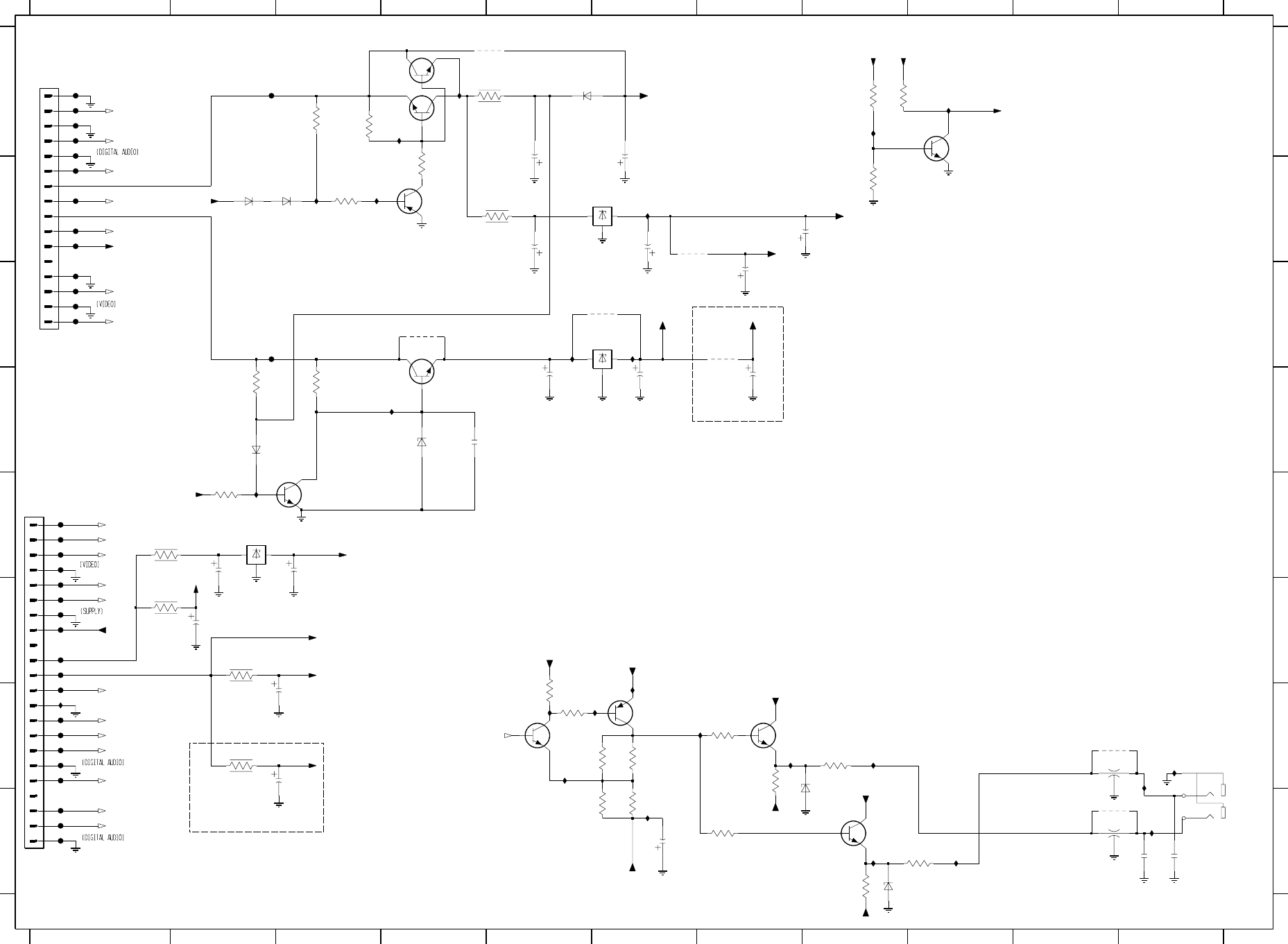
41 42
C3 : AV PCB
100u
7401 E2
7411 C6
7412 B6
7413 A4
F508 A1
F509 A1
F510 A1
F511 A1
F512 A1
F513 B1
F514 A2
F515 B1
F516 C2
F517 B1
F525 E1
F526 E1
F527 F1
F528 F1
3582 H8
3583 H9
3584 B5
4411 B6
4434 C4
4435 G10
4436 H10
4437 C6
4438 C7
4439 A5
5000 G10
5001 H10
6405 B2
6406 B3
F529 F1
F530 F1
F532 F1
F533 F1
F534 G1
F535 G1
F536 G1
F537 G1
F538 G1
F539 G1
F540 G1
F542 H1
F543 H1
F544 H1
I503 B3
I504 B3
I505 A4
7038 H8
2503 B6
2504 C7
2505 B8
3553 A3
3554 A3
3555 B3
3556 B4
3557 A5
3558 A8
3559 A8
3560 B8
3561 E2
3562 D2
3563 D3
F518 B1
F519 C1
F520 C1
F521 C1
F522 C1
F523 E1
*
(BC 848B)
(BC 8 4 8 B)
FOR KOK ONLY
(BC8 5 8 B)
*
FOR
*
F524 E1
3581 G8
4 5 6 7 8 9 10 11
1 23456
6407 A5
6408 H8
6409 D2
6410 H8
6414 D4
7030 A4
COLOR SETTING
(BC 8 4 8 B)
7031 B4
7032 A9
7033 D4
7034 E3
7035 G5
7036 G6
7037 G7
2502 B5
A
B
C
D
E
F
G
H
1000 A1
1001 E1
1401-A G11
2486 A5
2487 A6
2488 D4
3566 E1
3567 F1
3568 F2
3569 G2
3572 G5
3573 G5
(BC 848B)
(BC337-40)
*
*
3574 G6
3575 G6
3576 H6
3577 H6
3578 G7
3579 H7
3580 G7
3
I510 A9
I511 E2
I512 D4
I514 D5
I515 C6
I516 G5
I517 G6
I518 G5
I519 G6
I520 H6
I521 G7
I522 G7
I523 G8
I524 H8
7891011
2494 F2
*
#
#
#
(BC 848B)
2495 G2
2496 G2
2499 H6
2500 H11
2501 H11
H
I531 B6
#
FOR DVD 732
*
Reserved Parts
*
A
B
C
D
E
F
G
I506 A4
2489 D5
2490 D6
2491 D7
2492 E2
2493 E3
*
#
*
*
*
*
*
(BC858B)
*
12
I509 A8
LF33CV
7401
GND
IN OUT
0R
I525 H9
I526 G11
I527 H11
I528 G11
3553
I509
10K
3567
4R7
I506
4434
I505
270R
3572
I504
F508
47u
F542
F533
2493
F530
F532
I531
I526
0|6|12
I519
4439
I527
4K7
3556
3554
4K7
F544
I515
F539
3579
100R
220p
2500
F526
F527
F519
100u
+5VVID
3569
4R7
2496
I522
I520
I521
3576
4K7 680R
3577
10u
2492
I517
I518
-5VA
BC847B
7036
BC857B
F511
F535
7037
I514
2501
I528
75R
3583 220p
BZX284-C15
6410
3
1
2
4435
F525
F534
YKC21-4040
1401-A
+5VVID
I524
-5V
I516
I523
F523
7412
GND
IN OUT 2505
100u
25
4R7
4411
MC79M05
100u
2504
3584
10u
2503
25
10u
22u
2502
2490
4K7
3562
13
DSS306
5001 2
13
DSS306
5000 2
3563
4K7
3561
+6Vstby
2K2
7032
BC847B
7034
100u
2494
BC847B
6K8
3574
BC847B
F522
100R
3573
7035
3581
2487
100u
25
6408
BZX284-C15
75R
+6Vstby
-5V
47u
2491
F509
10u
2489
GND
IN OUT
F536
7411
LF80CV
-5V
4K7
3559
F537
100R
4436
3578
7033
BC547B
I525
4R7
3557
6409
BAS216
BAS216
6407
4437
3568
6405
BAS216
47u
2486
9
2K2
3582
1
10
11
12
13
14
15
16
2
3
4
5
6
7
8
7031
52030
1000
25
100u
2499
-5V
BC857B
BC547B
7413
F520
F521
F517
F518
F515
2K2
3580
F513
F543
F512
2K7
3560 3558
4K7
F529
F538
F528
+8VHP
F524
F516
I510
-8VHP
I511
2495
7038
BC847B
4R7
3566
I512
5
6
7
8
9
+8V_VID
F514
11
12
13
14
15
16
17
18
19
2
20
21
22
3
4
1001 1
10
6406
3575
820R
7030
BC817-25
BAS216 I503
3555
4K7
2488
470n
4438
6414
BZX284-C9V1
F540
F510
CVBS
CVBS_2
CVBS_1
3V3
+5VD
+5V
+5VVID
P50
KILL
PCM_OUT0
LRCLK
SCLK
PCM_CLK
B
STEREO_MUTE
DIG_OUT
G
R
CVBS
+5VA
H_SYNC
PCM_OUT2
PCM_OUT1
SCL
SDA
+6Vstby
C
Y
DC_OFF
+5V +6Vstby
DC_OFF
DC_OFF
CL06532021_008.eps
230200
A/V board (A1B, /S1G, /U1B)
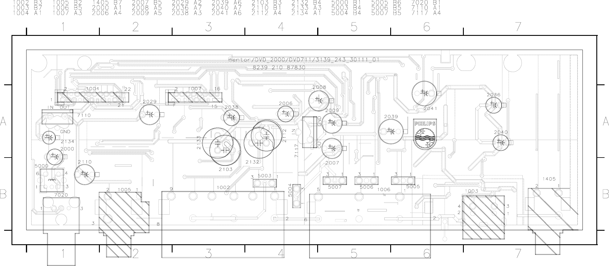
43 44
A/V Pwb (A1B, /S1G, /U1B)
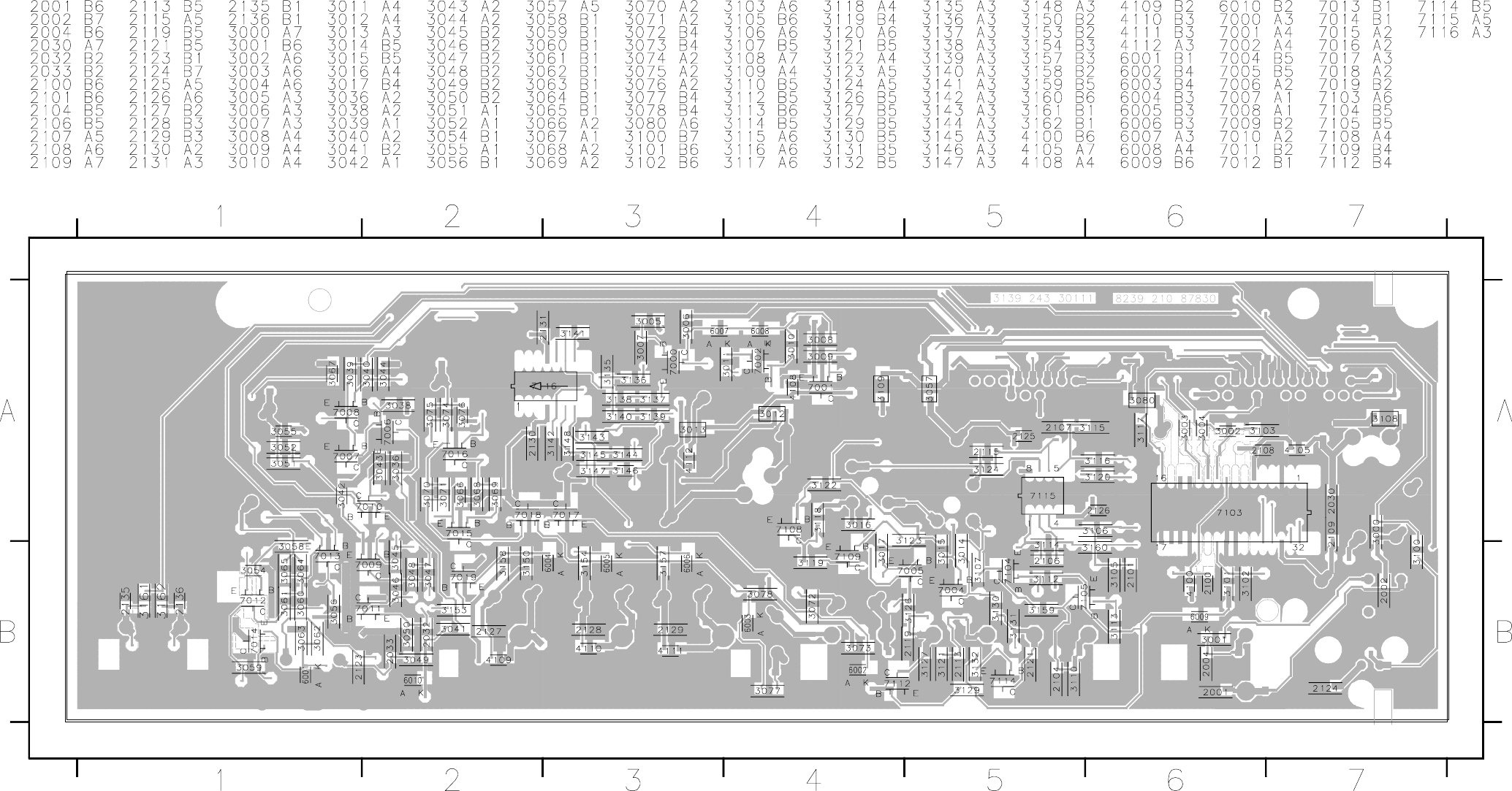
45 46
A/V Pwb (A1B, /S1G, /U1B)
47 48
12. TROUBLESHOOTING
DISPLAY PCB OK.
NO DISC
POWER ON
DISPLAY?
Check presence of high pulses at pin 23 of IC7104 while pressing a key on remote control.
Check IR receiver 6610.
Check safety resistor R3131.
Diagnostic software “Player script” : Remote control test.
Check if voltage at connector 1117-1 is 4.9V when power on (no light)
Check if voltage at base of Tr 7109 is 4.9V when power on (no light).
Check if voltage at connector 1117-1 is 3.33V during standby (light).
Diagnostic software “Player script” : LED test.
Check matrix scanning at pin 36 and 37: see test instructions.
Check matrix scanning at pin 26,27,28,29,30,31,32,33.
Diagnostic software “Player script” : Keyboard test.
Check supply voltages
The display pcb uses a 24V stabiliser(7112) in combination with a 10V zenerdiode(6102).
Check input voltage: at connector 1115-4: -40V 5%
Check output voltage at anode of Diode 6102: -10V 5%
Check stabilizer 7112 output (VKK): -34V 7%
Check +5Vstb voltage at connector 1115-3: +5V 5%
Check safety resistor R3117
Check +12V at connector 1115-1: +12V 10%
Check filament voltage
AC voltage is created via uP output pin 19 generating a 42kHz (duty cycle 45/55) square
signal.
Check frequency : 42kHz 10%
Check buffered square output at emitter of transistor 7105; low level: 800mV, high level:
10.7V
Check DC decoupling: check RMS voltage between FIL1 and FIL2 lines:
3.9Vrms<Vfil<5.2Vrms
The Vfil_DC level at kathode of diode 6101 should be –25.8V 10%
Check oscillator frequency of 8MHz at pin 8 of IC7104
Check reset circuit around transistor 7108: see test instructions of reset circuit.
Check timing and level for all grid lines(G1 G14): see test instructions grid lines.
Check timing and level of segment lines(P1 P10): see test instructions segment lines.
Diagnostic software “Player script” : Display test.
NO
YES
Key Function NO
YES
Standby LED off?
YES
Remote control? NO
YES
NO
Testing of A/V board can be done using diagnostic software “Player script”.
Mono board is used to generate a sinus with the soundtest SND-2 or a VIDEO signal with the picture test PIC-1.
See description in chapter “Diagnostic Software : Script Interfaces”
SOUND OK
Diagnostic Software
NO SOUND ON
AUDIO CINCH 1402
POWER SUPPLY?
Check DAC IC 7401
Check C2455, C2459, C2461, C2464 NP0 TYPE?
Check OPAMP 7403
Check ELCO'S 2456, 2462
Check OPAMP 7403
Check KILL transistors 7404, 7405, 7406, 7407
Check resistors 3453, 3464
Check OPAMP 7403
Check KILL transistors 7404, 7405, 7406, 7407
Check DAC IC 7401
Check VREFA on pin 30 of DAC 7401
Check testpoints 7, 8, 9, 10
Check flex connection to mono board
Check mono board
Check supply voltages 3V3(7400), +8Vaud(7304), -8Vstby,
+12Vstby
Check flex connection to mono board.
NO
YES
PCM_OUT0
LRCLK, SCLK
PCM_CLK
NO
YES
NO
YES
AUDIO
CINCH OUTPUT
TP 13?
NO
YES
AUDIO
TP 12?
NO
YES
LEVEL OK?
YES
N0
DISTORTION?
To put set in “Player script”, press keys
STOP+OPEN/CLOSE simultaneously and connect to
mains. Proceed until display shows “”.
AUDIO PART
TROUBLESHOOTING DISPLAY BOARD TROUBLESHOOTING A/V BOARD
APP SND-2 APP SND-2
49 50
SOUND OK
Diagnostic Software
NO SOUND ON
TV- & AUX-SCART
AUDIO TP14?
Check supply voltage of IC7917(D6401)
Check Scart switching IC7917
Check Elco's 2372, 2373
Check OPAMP 7403
NO
YES
AUDIO
TP 15?
NO
YES
To put set in “Player script”, press keys
STOP+OPEN/CLOSE simultaneously and connect to
mains. Proceed until display shows “ ”.
DIGITAL OUT OK
Diagnostic Software
NO DIGITAL OUTPUT
DIG_OUT TP11?
Check digital trafo L5400
Check flex connection to mono board
Check mono board
NO
YES
DIGITAL OUT
TP18?
NO
YES
To put set in “Player script”, press keys
STOP+OPEN/CLOSE simultaneously and connect to
mains. Proceed until display shows “ ”.
OPTICAL OUT? Check +5V supply(R3803)
Check optical transmitter 6400
APP SND-2 APP SND-2
APP SND-2 APP SND-2
VIDEO PART OK
Diagnostic Software
NO PICTURE
CVBS & Y/C OUT
POWER SUPPLY?
Check VIDEO buffers
See test instructions
Check VIDEO buffers
See test instructions
Check flex connection to mono board
Check mono board
Check supply voltages +8Vstby, –8Vstby, +12Vstby, +6V,
+5V
Check voltage regulator 7304
Check safety resistors 3615, 3620, 3802, 3803
Check flex connection to mono board.
NO
YES
VIDEO
TP1-6?
NO
NO
YES
YES
NO
YES
VIDEO
Y/C OUT
TP20-21?
VIDEO
CVBS CINCH
TP19?
To put set in “Player script”, press keys
STOP+OPEN/CLOSE simultaneously and connect to
mains. Proceed until display shows “ ”.
VIDEO PART
APP PIC-1 APP PIC-1
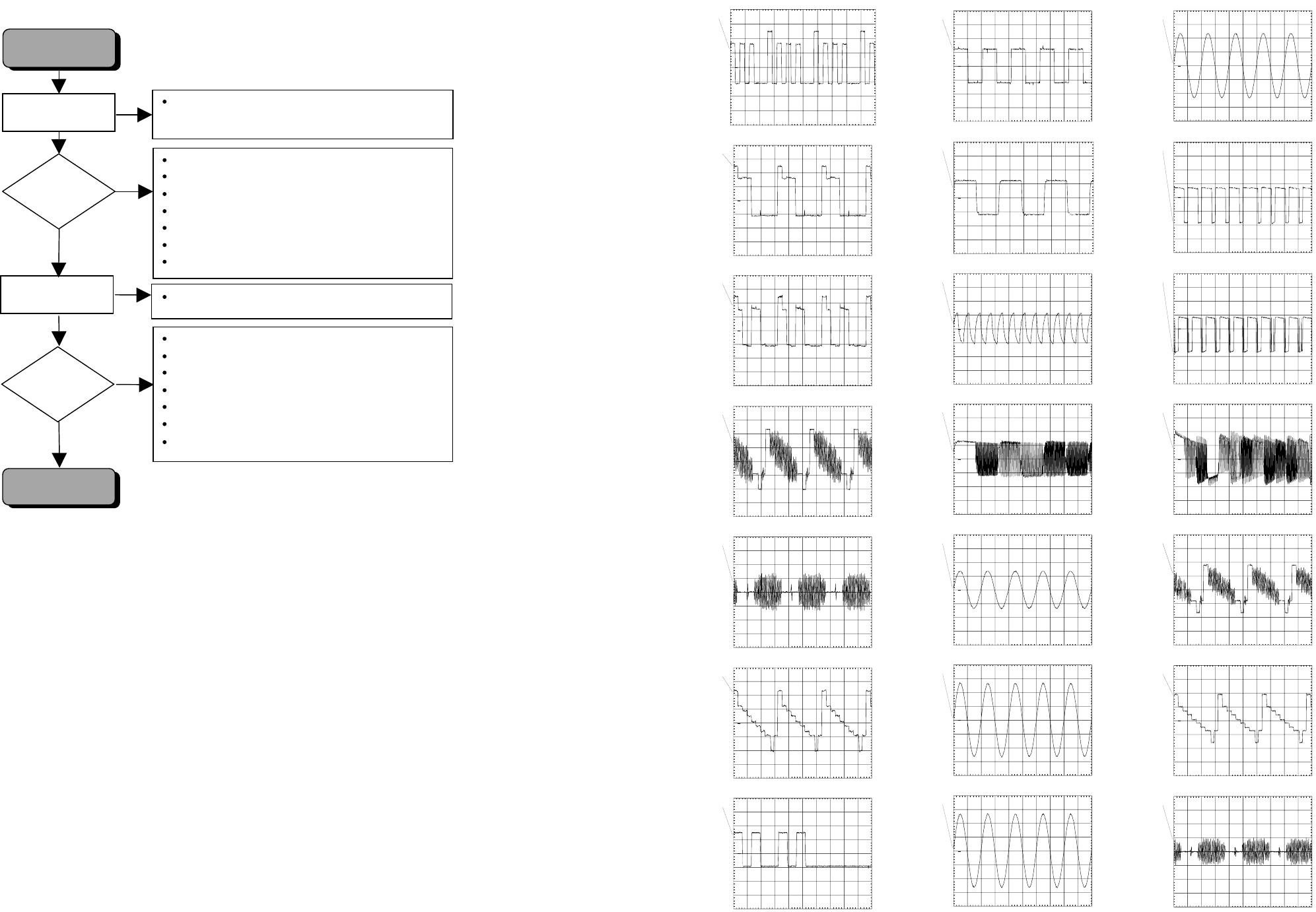
51 52
SCART SWITCHING
OK
Diagnostic Software
NO PICTURE SCART
SCART SWITCHING
PICTURE TV?
Check “0/6/12” on connector 1300-8 = +10V
Check flex connection to mono board
Check “SELECT” = 0V, “SELECT HIGH” = 0V
Check transistors 7935, 7943
Check switches 7900-7905
Check “SLB_TV: 9V, “FBOUT_TV: 5V
Check video buffers, see test instructions.
NO
YES
NO
YES
PICTURE
AUX/VCR IN
ON TV?
To put set in “Player script”, press keys
STOP+OPEN/CLOSE simultaneously and connect to
mains. Proceed until display shows “ ”.
Diagnostic Software press NEXT. Display shows:” Pressing
PREVIOUS will return to “
Check “0/6/12” on connector 1300-8 = 0V
Check flex connection to mono board
Check “SELECT” = 6V, “SELECT HIGH” = 12V
Check transistors 7935, 7943
Check switches 7900-7905
Check “SLB_TV = 0V, “FBOUT_TV = 0V.
Check video buffers, see test instructions.
SCART DVD SCART DVD
SCART DVD
SCART LOOP SCART LOOP
PM3392A
ch1
CH1 200mV~ MTB20.0us ch1+
1
TP 1 : video B
PM3392A
ch1
CH1 200mV~ MTB20.0us ch1+
1
TP 2 : video G
PM3392A
ch1
CH1 200mV~ MTB20.0us ch1+
1
TP 3 : video R
PM3392A
ch1
CH1 200mV~ MTB20.0us ch1+
1
TP 4 : CVBS
PM3392A
ch1
CH1 200mV~ MTB20.0us ch1+
1
TP 5 : C_ENC
PM3392A
ch1
CH1 200mV~ MTB20.0us ch1+
1
TP 6 : Y_ENC
PM3392A
ch1
CH1 2 V~ MTB 500ns ch1+
1
PM3392A
ch1
CH1 2 V~ MTB10.0us ch1+
1
PM3392A
ch1
CH1 2 V~ MTB 100ns ch1+
1
PM3392A
ch1
CH1 2 V~ MTB 100ns ch1+
1
PM3392A
ch1
CH1 2 V~ MTB 100ns ch1+
1
TP 11: DIG_OUT
PM3392A
ch1
CH1 1 V~ MTB 500us ch1+
1
TP 12 : ANALOG OUTPUT DAC
PM3392A
ch1
CH1 1 V~ MTB 500us ch1+
1
TP 13 : ANALOG OUTPUT AUDIO CINCH
PM3392A
ch1
CH1 1 V~ MTB 500us ch1+
1
TP 14 : ANALOG OUTPUT AUDIO HP_R & HP_L
PM3392A
ch1
CH1 1 V~ MTB 500us ch1+
1
TP 15 : AUDIO SCART SWITCH OUTPUT
PM3392A
ch1
CH1 2 V~ MTB50.0ms ch1+
1
PM3392A
ch1
CH1 2 V~ MTB50.0ms ch1+
1
PM3392A
ch1
CH1 200mV~ MTB 200ns ch1+
1
PM3392A
ch1
CH1 500mV~ MTB20.0us ch1+
1
TP 19 : CVBS_OUT
PM3392A
ch1
CH1 50mV~ MTB20.0us ch1+
1
PM3392A
ch1
CH1 500mV~ MTB20.0us ch1+
1
TP 21: C_OUT
TP 20: Y_OUT
TP18: DIGITAL OUT
TP17: SCL
TP16: SDA
TP8: LRCK
TP9: SCLK
TP10: PCM_CLK
TP7: PCM_OUT0
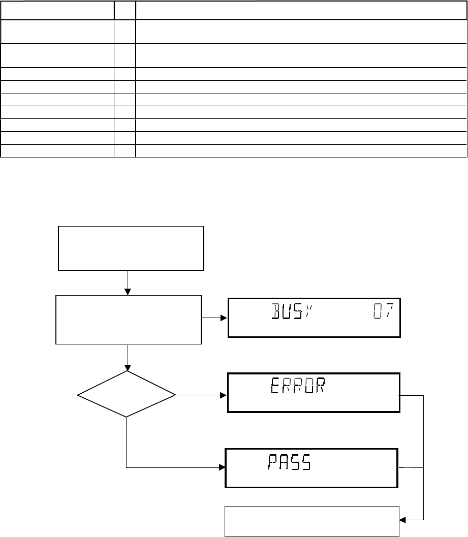
53
13. DIAGNOSTIC SOFTWARE : SCRIPT INTERFACES
13.1 DEALER SCRIPT
13.1.1 Purpose of Dealer Script
The dealer script can give a diagnosis on a standalone DVD
player; no other equipment is needed to perform a number of
hardware tests to check if the DVD player is faulty. The
diagnosis is simply a "error" or "pass" message; no indication
is given of faulty hardware modules. Only tests within the scope
of the diagnostic software will be executed hence only faults
within this scope can be detected.
13.1.2 Contents of Dealer Script
The dealer script executes all diagnostic nuclei that do not
need any user interaction and are meaningful on a standalone
DVD player.
The nuclei called in the dealer script are the following (the
number after each nucleus name corresponds with the number
being on the local display when the nucleus is executed during
the dealer script):
Figure 13-1
Figure 13-2
VideoColSetupComm Checks the I2C interface with the RGB video processor on the
Audio/Video board (only for DVD players with RGB video processor).
VideoScartSwComm Checks the I2C interface with the scart switch on the Audio/Video
board
PapChksFl Calculate and verify checksum of FLASH memory.
PapDramWrR Pattern test of all locations in the DRAM(s).
PapI2cDisp Checks the I2C interface with the slave processor on the display PCB.
PapS2bEcho Checks the I2C interface to the basic engine.
PapI2cNvram Checks the I2C interface with the NVRAM.
PapNvramWrR Pattern test of all locations in the NVRAM
CompSdramWrR Pattern test of all locations in the SDRAM(s).
Nucleus
Description
Press 2 keys simultaneously
<OPEN/CLOSE> + <PAUSE>
Connect to mains.
During the test, the following display
is shown: the counter counts down
from the number of nuclei to be run
before the test finishes. Example:
SET O.K.?
YES
NO
To exit DEALER SCRIPT ,disconnect from mains.
54
13.2 PLAYER SCRIPT
13.2.1 Purpose of Player Script
The Player script will give the opportunity to perform a test that
will determine which of the DVD player's modules are faulty, to
read the error log and error bits and to perform an endurance
loop test. To successfully perform the tests, the DVD player
must be connected to a tv set to check the output of a number
of nuclei. For DVDv2b a multi-channel amplifier, a set of 6
boxes and an external video source are necessary to test. To
be able to check results of certain nuclei, the player script
expects some interaction of the user (i.e. to approve a test
picture or a test sound). Some nuclei (e.g. nuclei that test
functionality of the Basic Engine module) require that the DVD
player itself is opened, to enable the user to observe moving
parts and approve their movement visually. Only tests within
the scope of the diagnostic software will be executed hence
only faults within this scope can be detected.
13.2.2 Contents of Player Script
The player script contains all nuclei that are useful on a DVD
player that is connected to a tv-set and help to determine which
module of the DVD player is faulty, as well as to read out the
contents of the error logs.
13.2.3 Structure of Player Script
The player script consists of a set of nuclei testing the three
hardware modules in the DVD player: the Display PWB, the
Digital PWB and the Basic Engine.
Nuclei run by the player test need some user interaction; in the
next paragraph this interaction is described. The player test is
done in two phases:
1. Interactive tests: this part of the player test depends
strongly on user interaction and input to determine nucleus
results and to progress through the full test. Reading the
error log and error bits information can be useful to
determine any errors that occurred recently during normal
operation of the DVD player.
2. The loop test will perform the same nuclei as the dealer
test, but it will loop through the list of nuclei indefinitely.
13.2.4 Survey
Figure 13-3
SLEDGE TEST
BeSledgeOut/In(41ab)
FOCUS TEST
BeFocusOn(38a)
DISC MOTOR TEST
BeDiscMotorOn(39a)
RADIAL TEST
BeRadialOn(40a)
JUMP TEST
BeGroovesIn/Mid/Out(42abc)
Press 2 keys simultaneously
<OPEN/CLOSE> + <STOP>
Connect to main
s
To exit player test,
disconnect from mains
INTERACTIVE TESTS
DISPLAY TEST
DispDisplay(30)
LED TEST
DispLed(29)
KEYBOARD TEST
DispKeyb(27)
SCART LOOP TEST
AudioPinkNoiseOn(20a)
VideoScartSwDvd(54a)
VideoColDencOn(23a)
PICTURE TEST
DISPLAY PCB
MONO PCB(SERVO)
& BASIC ENGINE
MONO PCB
DIGITAL PART
TRAY TEST
BeTrayOut/In(43ab)
VERSION NUMBER
BeVer(37)
REMOTE CONTROL
DispRc(28)
TRAY TEST
BeTrayOut/In(43ab)
ERROR LOG & BITS
LogReadErr(31)
LogReadbits(32)
LOOP TEST
= Dealer script exclusive of test2
AudioSineOn(21a)
SOUND 1 TEST
SCART DVD TEST
SOUND 2 TEST
VideoScartSwPass(54b)
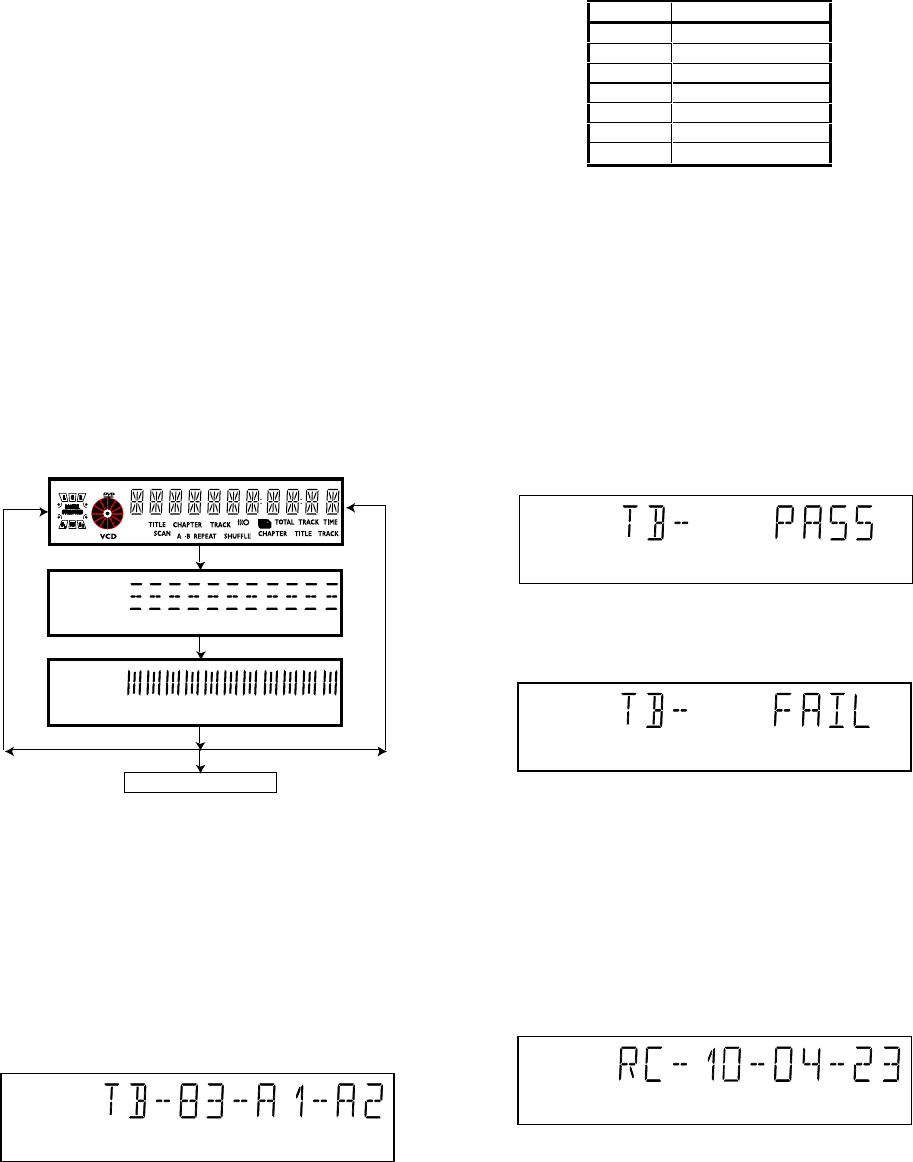
55
14. INTERACTIVE TESTS
14.1 DISPLAY PCB
14.1.1 DISPLAY TEST
The display test is performed by nucleus DispDisplay. By
putting a series of test patterns on the local display, the local
display is tested. To step through all different patterns, the user
must either press PLAY (pattern is ok) or PAUSE (pattern was
incorrect) to proceed to the next pattern. The display of
patterns is continued in a cyclic manner until the user presses
NEXT. If the user presses NEXT before all display patterns are
tested, the DispDisplay nucleus will return TRUE (display test
successful).
14.1.2 LED TEST
The LED(s) on the DVD player is (are) tested by nucleus
DispLed. The user must check if the LED(s) is (are) lighted; if it
is, press PLAY, if it is not, press PAUSE. By pressing NEXT the
script will proceed to the next test. If the user presses NEXT
before PLAY or PAUSE, the DispLed nucleus will return TRUE
(LED test successful).
Figure 14-1
14.1.3 KEYBOARD TEST
The keyboard of the DVD player is tested by nucleus
DispKeyb. The user is expected to press all keys on the local
keyboard once. The code of the key pressed is shown on the
local display (1 hexadecimal digit) immediately followed by a
(hexadecimal) number indicating how many times that key has
been pressed. Example of the local display during this test:
Figure 14-2
The key-codes displayed on the local display will scroll from
right to left when the display gets full, the text "tb-" will remain
on display.
Figure14-3
If any keys are detected more than once (due to hardware
error), the key-code is displayed twice (or more), with the
second digit increased by 1.
If the user does not press all keys minimally once (in any order),
the DispKeys nucleus will return FALSE and cause an error in
the overall result of the player script.
The user can leave the keyboard test by pressing the NEXT
key on the local display of the DVD player for at least one full
second.
The result of the keyboard test is shown on local display as
follows:
Figure 14-4
Or
Figure 14-5
Pressing NEXT on the local keyboard again will proceed to the
next text.
14.1.4 REMOTE CONTROL TEST
The remote control of the DVD player is tested by nucleus
DispRc. The user must press any key on the remote control just
once. The codes of the key pressed will be shown on the local
display in hexadecimal format. Example:
Figure 14-6
If OK, press PLAY If NOK, press PAUSE
If OK, press PLAY If NOK, press PAUSE
If OK, press PLAY If NOK, press PAUSE
press NEXT to continue
key id. key
0PLAY
1NEXT
2 PREVIOUS
3 PAUSE
4STOP
5
SOUND
6OPEN / CLOSE
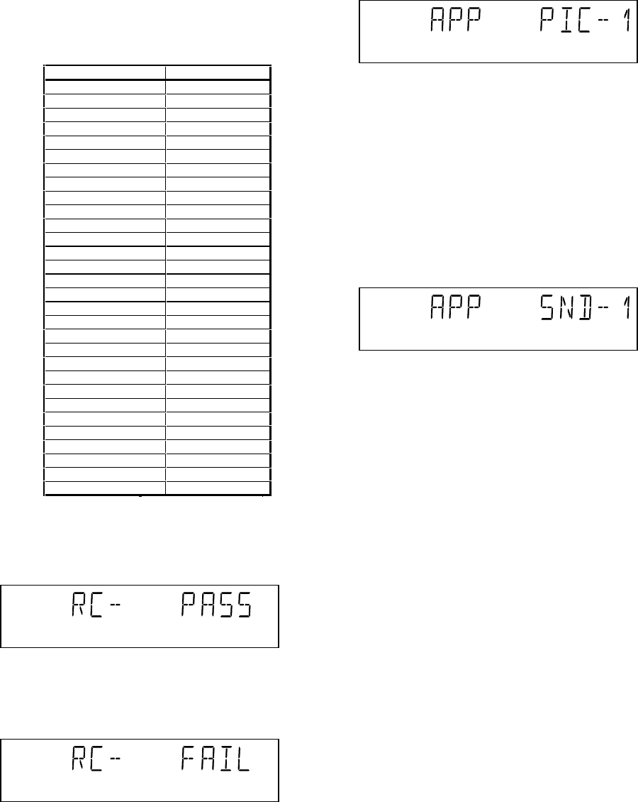
56
In this example 23 is the hexidecimal code of the pressed RC
key. The user can leave the remote-control test by pressing
NEXT on the local keyboard of the DVD player. The remote
control test is successful if a code was received before the user
pressed the NEXT key; pressing the NEXT key before pressing
a key on the remote control gives an error in the remote control
test (note that the remote control test will also fail if a key on the
remote control was pressed but no code was received). The
remote control test does not check upon the contents of the
received code, that is it will not be checked if the received code
matches the key pressed. If desired, the user can manually
check this code by using a code-table for the remote control
key-codes.
Figure 14-7
After pressing NEXT, the result of the remote control test is
displayed on the local display of the DVD player as follows:
Figure 14-8
Or
Figure 14-9
Pressing NEXT on the local keyboard again will proceed to the
next test.
14.2 MONO PCB DIGITAL PART
14.2.1 PICTURE TEST
The picture test is performed by putting a predefined picture
(colour bar) on the display (nucleus VideoColDencOn) and
asking the user for confirmation. The display will show the
following message:
Figure 14-10
By pressing PLAY the user confirms the test, pressing PAUSE
will indicate the picture was invisible or incorrect. Pressing
NEXT will proceed to the next test
14.2.2 SOUND 1 & SCART DVD TEST
The first soundtest is performed by starting a pink noise sound
that needs confirmation from the user (nucleus
AudioPinkNoiseOn); the display will show the following
message very shortly:
Figure 14-11
This sound will only be audible from version cut3.1 of
Sti5505(item7503 on mono board) onwards. After starting up
sound 1, SCART loop-trough will be simultaneously active
during this test. SCART loop-trough will be measured with the
aid of an external video source.
When entering the SCART loop-trough, the local display
indicates:
RC Key id Hexadecimal code
STANDBY C
STOP 31
PLAY 2C
PAUSE 30
NEXT 20
PREVIOUS 21
CURSOR UP 58
CURSOR DOWN 59
CURSOR LEFT 5A
CURSOR RIGHT 5B
OK 5C
00
11
22
33
44
55
66
77
88
99
ANGLE 85
AUDIO 4E
SUBTITLES 4B
ROOT MENU 54
OSD ON/OFF F
RETURN 83
SHUFFLE 1C
REPEAT 1D
A/B REPEAT 3D
57
Figure 14-12
On the TV screen a colour bar (generated by nucleus
VideoColDencOn) is visual and the internally generated
pinknoise is audible. By pressing PLAY the user confirms the
test, pressing PAUSE will indicate the sound was inaudible or
incorrect. Pressing NEXT will proceed to the next test; if the
user presses NEXT without pressing PLAY or PAUSE first, the
result of this test will be TRUE (sound ok). By pressing the
NEXT button there will be switched over to the external source,
this must become now visible on the TV screen (using the
SCART). The local display indicates:
Figure 14-13
The internally generated colour bar is still available on the
CVBS and Y/C outputs. And the pinknoise-signal is still
available on the cinch audio outputs. By pressing the PREV
button, the internal generated colour bar becomes visual again.
The test can be left by pressing the NEXT key for more than
one second.
14.2.3 SOUND 2 TEST
The second soundtest is performed by producing a sine sound
(nucleus AudioSineOn). The signal can be stopped by pressing
the STOP-key. The display will show the following message:
Figure 14-14
By pressing PLAY the user confirms the test, pressing PAUSE
will indicate that something went wrong. Pressing NEXT will
proceed to the next; if the user presses NEXT without pressing
PLAY or PAUSE first, the result of this test will be TRUE (sound
ok).
14.3 BASIC ENGINE
14.3.1 VERSION NUMBER
In the basic engine tests, the version number of the Basic
Engine will be shown first, as the following example:
Figure 14-15
By pressing the NEXT key, the Basic Engine tests are started.
14.3.2 TRAY TEST
First, the tray is tested. The purpose of this test is also to give
the user the opportunity to put a disc in the tray of the DVD
player. Some tests on the Basic Engine require that a disc(e.g.
DVD MPTD test disc) is present in the player. At the end of the
Basic Engine tests this tray test will be repeated solely to
enable the user to remove the disc in the tray. The local display
will look as follows:
Figure 14-16
By pressing PLAY or PAUSE the user can toggle the position
of the tray. Note that this test will not contribute to the test result
of the Basic Engine. Pressing NEXT will proceed to the next
test, after the tray has been closed (by the software) if it was
open.
14.3.3 SLEDGE TEST(visual test)
The second Basic Engine test tests the sledge; the user can
move the sledge as many times as desired by using PLAY
(nucleus BeSledgeOut) and PAUSE (nucleus BeSledgeIn).
Pressing NEXT on the local keyboard proceeds to the next test.
Note that this test will not contribute to the test result of the
Basic Engine. The local display will look as follows during the
sledge test:
Figure 14-17
14.3.4 DISC MOTOR TEST(visual test)
The third Basic Engine test tests the disc motor (nucleus
BeDiscMotorOn); the local display looks as follows:
58
Figure 14-18
By pressing PLAY the user confirms that the disc motor is
running; pressing PAUSE indicates the disc motor does not
work. Pressing NEXT proceeds to the next test, after a reset of
the disc motor (nucleus BeDiscMotorOff). If the user presses
NEXT before pressing PLAY or PAUSE, the result of this test
will be TRUE (disc motor is running).
14.3.5 FOCUS TEST(visual test)
The fourth Basic Engine test tests the focussing; first focussing
is turned on by calling nucleus BeFocusOn. The display will
look as follows:
Figure 14-19
By pressing PLAY the user confirms that the focussing was
succesful; pressing PAUSE indicates a focussing failure.
Pressing NEXT proceeds to the next test after a reset of the
focussing (nucleus BeFocusOff); if NEXT is pressed before
PLAY or PAUSE, the result of this test will be TRUE (focus
successful).
14.3.6 RADIAL TEST(visual & listening test)
The fifth Basic Engine test tests the radial functionality (nucleus
BeRadialOn); the local display looks as follows:
Figure 14-20
By pressing PLAY the user confirms that the radial function
worked; pressing PAUSE indicates the function does not work.
Pressing NEXT proceeds to the next test, after a reset of the
radial (nucleus BeRadialOff). If the user presses NEXT before
pressing PLAY or PAUSE, the result of this test will be TRUE
(radial successful).
14.3.7 JUMP TEST(listening test)
The sixth and last Basic Engine test tests the jumping by calling
nuclei BeGroovesIn, BeGroovesMid and BeGroovesOut.
During this test, the local display looks as follows:
Figure 14-21
The user can switch between the three different types of
groove settings by pressing PLAY (forward to next nucleus in
the list In-Mid-Out) or PAUSE (backward in the list In-Mid-Out).
This is done in a cyclic manner; note that this test will not
contribute to the test result of the Basic Engine. Pressing NEXT
proceeds to the next test, after the disc motor has been shut off
with a call to nucleus BeDiscMotorOff.
14.3.8 TRAY TEST
As a last action for the Basic Engine tests, the tray test is
repeated. The local display will look as follows:
Figure 14-22
This test is meant to give the user the opportunity to remove the
disc in the tray. The tray position can be toggled using the
PLAY and PAUSE key. The tray will be closed (by the software,
if it is open) before proceeding to the next test when the user
presses the NEXT key.
59
14.3.9 ERROR LOG
Reading the error log and error bits information can be useful
to determine any errors that occurred recently during normal
operation of the DVD player. Reading the error log is done by
nucleus LogReadErr. The display during the errorlog readout
looks as follows :
Figure 14-23
By pressing PLAY or PAUSE the user can move forward or
backward (respectively) through the logged error codes. The
highlighted number indicates which errorcode is currently on
display (in the example above, errorcode number 4 is
displayed). If "0000" is displayed at all positions, the error log is
empty. Display of the logged errors is done in a cyclic manner.
The errorcode with the lowest highlighted number is the most
recent. By pressing NEXT on the local keyboard, the user can
proceed to the next test.
14.3.10 ERROR BITS
Reading the error bits is done by nucleus LogReadBits. The
display during the errorbits readout looks as follows:
Figure 14-24
Only the set errorbits will be shown by their (decimal) number.
Refer to the appropriate documentation for the explanation of
each bit number. If the display only shows "EB-0", no error bits
were set. By pressing NEXT the user can continue to the next
test.
See table below:
Error log / bits table Read ERROR LOG in player
script
Read ERROR BITS in
player script
Basic engine errors Value: Value:
Command to the Basic Engine not allowed in this state or unknown
command
150101 8
Parameter(s) from the command to the Basic Engine is not valid 150102 7
Sledge could not be moved to the inner home position 150103 6
Focus failure 150104 5
Turntable motor speed could not be reached within timeout 150105 4
Radial servo could not get on track on the disc 150106 3
PLL could not lock in the accessing or tracking state 150107 2
Subcode or sector information could not be read 150108 1
requested subcode could not be found 150109 16
Tray could not be closed or opened completely 15010A 15
TOC could not be read within timeout 15010B 14
The requested seek on the disc could not be executed 15010C 13
A requested lead-in is not on the disc 15010D 12
A non existing burst cutting area is requested 15010E 11
S2b communication error 1501F0 10
S2b communication error 1501F1 9
S2b communication error 1501F3 24
S2b communication error 1501F4 23
S2b communication error 1501F5 22
Digital PWB errors
Communication error with the Sti 5505 90000 32
Communication error with the Sti 5505 90001 31
Disply processor errors
Communication error with the display processor 190000 40
60
14.4 LOOP TEST
At the start of the loop test, the display will show the result of
the interactive player test:
Figure 14-25
The left side of the display contains a 3-digit code, which can
have a value between 000 and 111. These values are to be
interpreted as follows:
Figure 14-26
The loop test will perform the same nuclei as the dealer test,
but it will loop through the list of nuclei indefinitely. The display
of the DVD player will display not only the three digits indicating
correct/faulty modules and the last found error code (as
mentioned, faults are detected as far as they can be within the
scope of the diagnostic software), but also a loop counter
indicating how many times the loop has been gone through.
Example:
Figure 14-27
The number after the hyphen indicates the number of times the
loop test has been performed; the 4 digits at the right side of the
display show the last error that was found when running the
loop test: the leftmost two digits of this code indicate which
nucleus resulted in a fault; the rightmost two digits refer to the
faultcode within that nucleus. For further explanation of this
error code, see list of error codes below.
Figure 14-28
Displayed
Value Indication for each module
Basic Engine Mono
PCB Display
PCB
000 ok ok ok
001 ok ok faulty
010 ok faulty ok
011 ok faulty faulty
100 faulty ok ok
101 faulty ok faulty
110 faulty faulty ok
111 faulty faulty faulty
FAULTY
MODULE(S)
LOOP
COUNTER NUCLEUS ERROR
ERROR CODES LOOP TEST
ERROR CODE NUCLEUS NUMBER ERROR DESCRIPTION
0601
6 Calculated checksum of FLASH is not correct
0901
9 The DVD DRAM is faulty
1104
11 I2C bus busy before start
1102
NVRAM access time-out
1103
No NVRAM Acknowledge
1104
NVRAM reply time-out
1201
12 I2C bus busy
1202
I2C bus not working
1203
Slave controller not responding
1204
Slave response is not correct
1301
13 Parity error from basic engine to serial
1302
Parity error from serial to basic engine
1303
No communication between serial and basic engine
1304
Communication time-out error
1601
16 The SDRAM is faulty
61
14.5 Servicing DVD module and MONO board
The DVD module(Basic Engine and the mono board) has to be
exchanged completely in case of failure. A new module for
DV4100 can be ordered with codenumber 3104 129 51980.
14.5.1 Reprogramming of new mono boards.
Figure 14-29
14.5.2 Reset of Virgin Mode
After the player has been powered up for test by the dealer, it
would have gone through the Virgin Mode. It is possible to reset
the settings made during that mode before the delivery of
player to the customer. This can be done as shown in the
following diagram:
Figure 14-30
Figure 14-31
Caution
This information is confidential and may not be distributed. Only a qualified service person should
reprogram the mono board
.
After replacement of the mono board, all the customer settings and also the region code will be lost.
Reprogramming of the mono board will put the player back in the state in which it has left the factory,
i.e. with the default settings and the allowed region code.
Reprogramming will be done by way of the remote control.
Put the player in stop mode, no disc loaded.
Reprogramming is limited to 25 times
When the counter reaches 25, reprogramming is not possible anymore
Press the following keys on the remote control:
<
PLAY
> followed by numerical keys
<2> <7> <4>
The display shows: “
- - - - - - - - - - -
”
Press now successively the following keys :
for DV4100/A1B :
<0><1><5> <0><0><0><0><0><0><0><0><0> PAL / NTSC
for DV4100/N1B :
<0><1><2> <0><0><0><0><0><0><0><0><0> PAL / NTSC
for DV4100/S1G :
<0><1><3> <0><0><0><0><0><0><0><0><0> PAL / NTSC
for DV4100/U1B :
<0><1><0> <0><0><0><0><0><0><0><0><0> PAL / NTSC
Press <
PLAY
> again.
The TV screen will become BLUE during a short time to confirm that the mono board has been
reprogrammed, then the set goes to standby mode.
DISCONNECT FROM MAINS
PRESS 2 KEYS
SIMULTANEOUSLY
<PREVIOUS> + <OPEN/CLOSE>
CONNECT TO MAINS
VIRGIN MODE IS RESET
TV SCREEN SHOWS
VIRGIN MODE MENU
DISCONNECT FROM MAINS
IF TRADE MODE OFF
PRESS 2 KEYS
SIMULTANEOUSLY
<PLAY> + <OPEN/CLOSE>
CONNECT TO MAINS
DISCONNECT FROM MAINS
IF TRADE MODE ON
PLAYER IS IN NORMAL MODE
WHEN PRESSING FRONT
KEYS, THE PLAYER WILL
RESPOND
PRESS 2 KEYS
SIMULTANEOUSLY
<PLAY> + <OPEN/CLOSE>
CONNECT TO MAINS
PLAYER IS IN TRADE MODE
WHEN PRESSING FRONT
KEYS, THE PLAYER
DOESN'T RESPOND
TRADE MODE
When the player is in Trade Mode, the player cannot be
controlled by means of the front key buttons, but only by means
of the remote control.
For /U1B with old DVD module "VAE3000". (Production
WEEK36 or earlier) For other DV4100
Please refer the DVD Module ADS-1 Service Manual (3122 785
10840) attached with this Service Manual.
For servicing DVD Module ADS-1, the service application
softwear "ComPair" is necessary.
62
15. TEST INSTRUCTIONS DISPLAY BOARD
15.1 Display board
15.1.1 Introduction
These test instructions are written for all versions of the display
PCB 3104 123 42230.
The contents of the PCB can be split up into next blocks:
Figure 15-1
15.1.2 Functionality description:
The essential component of the display PCB is the P (slave).
This slave works on an 8MHz resonator and has a reset circuit
that is triggered by the +5Vstby. After the reset pulse, the
standby control line will release the reset of the host P. This
host P will then initialise the slave. In addition, when going to
stand-by, the slave will put the host P in reset. When the slave
receives the right IR or key code to leave the standby mode, the
reset of the host P will be released.
Other slave functions are:
Square signal generator to generate the filament voltage,
which is required for an AC FTD.
Generates the grid and segment scanning for the FTD.
Generates a scanning grid for the keys (separated from
display scanning).
Has inputs for RC (RC5 and RC6) and P50 (P50 controller
is built in).
15.1.3 General
Oscilloscope measurements have been carried out using a
Philips PM3392A.
Impedance of measuring-equipment should be > 1M .
To do correct measurements we recommend to use supply
3122 427 21370, which is used in all "second generation B"
DVD-players. Make sure that the main 3.3V has a 0.7A
load.
15.1.4 Reset
Check next reset timing with an oscilloscope at pin 10 of the
microprocessor.
Figure 15-2
Timing: 400msec < T1 > 700msec.
CH1: +5Vstby voltage at power on.
CH2: Voltage at pin 10.
15.1.5 Display steerign
Check next timing and level for all grid-lines (G1 r G14).
Figure 15-3
1. Check level A: +4V5 +/-10% for grid lines 1 => 11
2. Check level A: +4V0 +/-10% for grid lines 12 => 14
3. Check level B: -33V +/-10%
4. Check timing and levels of segment-lines P1 => P10:
Figure 15-4
Processor
I2C
Display
Key-matrix
RC-Eye
V filament
V filament
Buffer
P50
I/O
Supply:
+5Vstby
+12V
-40V
PM3392A
ch1
ch2
CH1 2. 00 V=
CH2 2 V= BW L MTB 100 ms- 1.04d v ch2+
1
2
T
T1
PM3392A
ch1 ch1: low =-34.2 V
ch1: high= 3.98 V
STOP
CH1 10.0 V= MTB 200us 2324us ch1+
1
T
A
B
PM3392A
ch1
CH1 10. 0 V= BWL MTB 500u s- 1.04 dv ch1 +
1
T
A
B
63
Level A:+4V5 +/-10%
Level B:-33V +/-10%
The data on these segment lines depend on the characters that
are displayed.
The characters can be set by sending I2C commands to the
display.
See the Slave URS how to send a display command.
15.1.6 Key-matrix
Connect a extra 10k pull-up to pin 36 en 37 of the P and
check next matrix scanning at these pins.
Figure 15-5
Level A: 5.0V +/-7%
Level B: 0V +/-200mV
Check matrix scanning from pin 26 until 33 of the P.
The results should be the same as the diagram above.
15.1.7 I.R. receiver
Check at pin 23 of the P if this line switches from low (< 0.3V)
to high (> 4.5V), while pressing a key on a Philips RC5 or RC6
remote control.
15.1.8 P50 interface
P50 is a bi-directional serial interface, which is used for
communication between video equipment. For European sets,
this communication goes via pin 10 of the scart-bus. In other
regions, it can be a cinch bus at the back of the set.
1. Keep the P in reset by short-circuiting emitter and
collector of transistor 7108, via resistor 3100 and 3104
transistor 7101 is switched on.
2. Check the voltage at the P50 output connector 1118-5: <
200mV.
When the reset is released the P output-pin becomes low and
transistor 7101 is switched off.
1. Check the voltage at the P50 output connector 1118-5: 4V9
+/-5%.
2. Check also the P P50 input ( P pin 20): 5V +/-5%.
3. Connect the P50 line (connector 1118-5) to ground.
4. Check again the P P50 input ( P pin 20): <0V3.
PM3392A
ch1 ch1: low =-46.9mV
ch1: high= 5.09 V
STOP
CH1 2.00 V= MTB10.0ms ch1-
1
B
A
64
16. CURRENT MODE POWER SUPPLY 20PS203
16.1 Blockdiagram
Figure 16-1
16.1.1 Function description of the current mode power supply
MOSFET 7125 is used as a power switch controlled by the
controller IC 7110. When the switch is closed, energy is
transferred from the mains into the transformer. This energy is
then supplied to the load when the switch is opened. By control
of the switched-on time, the energy transferred in each cycle is
regulated so that the output voltages are independent of load
or input voltage variations. The controlling device MC44603P is
an integrated pulse width modulator. A clock signal initiates
power pulses at a fixed frequency. The termination of each
output pulse occurs when an analogue of the inductor current
reaches a threshold established by the error signal. In this way
the error signal actually controls the peak inductor current on
cycle-by-cycle basis.
16.2 General description of MC44603
The MC44603 is an enhanced high performance controller that
is specifically designed for Off-line and dc-to dc converter
applications. This device has the unique ability of automatically
changing operating modes if the converter output is
overloaded., unloaded, or shorted. The MC44603 has several
distinguishing features when compared to conventional SMPS
controllers. These features consist of a foldback facility for
overload protection, a standby mode when the converter output
is slightly loaded, a demagnetisation detection for reduced
switching stresses on transistor and diodes, and a high current
totem pole output ideally suited for driving a power MOSFET. It
can also be used for driving a bipolar transistor in low power
converters. It is optimised to operate in discontinuous mode but
can also operate in continuous mode. Its advanced design
allows use in current mode or voltage mode control
applications.
16.3 Pin connections
Figure 16-2
+6V Stand By
GNDs
Feedback
Voltage
Rsense
7201
7200
6230
6260
6250
6240
5131
7125
2121
REGULATION
EMI
FILTER
MAINS
+12V
-8V Stand By
RQ
S
OSC.
+
+
--
2.5V
Error
Amplifier
latch
Lightning
Protection
Rectifier
1
5
7
9
Soft-Start
Control Overvoltage
Mgmt
Mgmt
Demagnet.
Output
Sense
Current
Sense
Input Buffer
Supply Init
Out
Gnd
7110
6129
6132
Vc
+5V
2240
2260
Stand By
+5V Stand By
-40V
+3V3
GND
7233
2250
7236
2230
6210
2210
6220
Rref
R Frequency Standb
Voltage feedback I
n
Error Amp Output
R Power Standby
Sof-Start/Dmax/
Voltage Mode
Sync Input
Overvoltage Protection(OVP)
Current Sense Input
Demag. Detection
Foldback Input
107
CT
8 9
6
5
11
12
Output
Gnd
VC
VCC
3
4
2
14
13
15
116
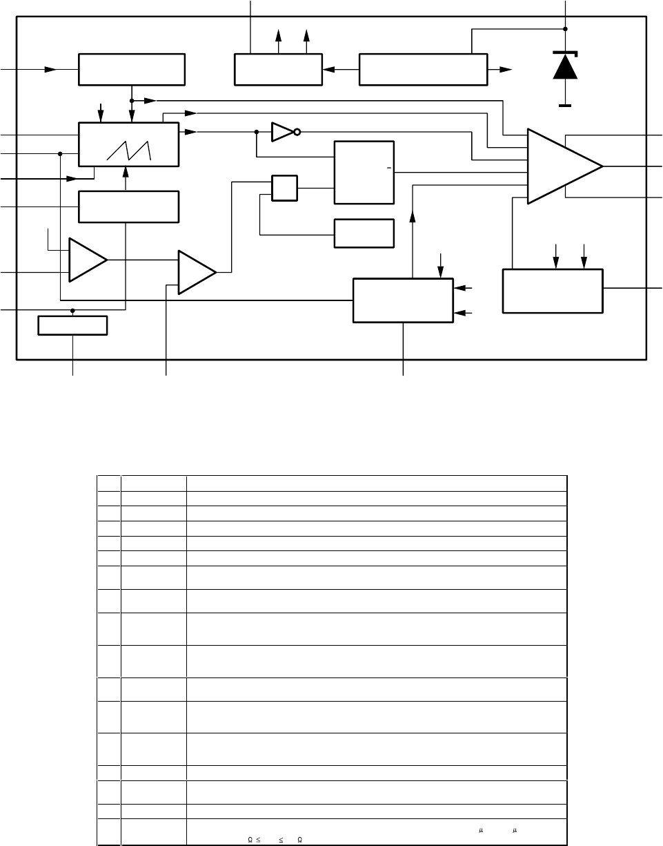
65
16.4 Blockdiagram of MC44603
Figure 16-3
16.5 Pin function description
Figure 16-4
VS8 OUT
CONTROL
Dmax &
SOFT-START
Vref
Voc
GND
OUT
VC
PROTECT
VOLTAGE
OVER
MANAGEMENT
OVER
VOLTAGE
DEMAGNETISATION
MANAGEMENT
OSCILLATOR
STANDBY
(REDUCED FREQUENCY)
ERROR
AMP CURRENT
SENSE
DEMAGNETISATION
DETECT
SYNC INPUT
CT
RF STANDBY
Iref
REFERENCE
BLOCK
SUPPLY
INITIALISATION BLOCK
Vref Iref
Vref
enable
UVL01
VOSC
VOSC PROT
=1
LATCH
THERMAL
SHUTDOWN
BUFFER
VOLTAGE
FEEDBACK
2.5V
RP STANDBY
Iref
UVL01
Vref
FOLDBACK
FOLDBACK
INPUT CURRENT SENSE
INPUT SOFT-START
& DMAX
1
2
3
4
6
57 11
8
9
10
15
12
14
13
E/A OUT
16
C
1Set
1Reset
Vstby
MC44603P
Pin function description
Pin Name Description
1 VCC This pin is the positive supply of the IC. The operating voltage range after start-up is 9.0 to 14.5 V.
2 VC The output high state (VOH) is set by the voltage applied to this pin.
3 Output Peak currents up to 750 mA can be sourced or sunk, suitable for driving either MOSFET or Bipolar transistors.
4 Gnd The groundpin is a single return, typically connected back to the power source.
5 Foldback Input The foldback function provides overload protection.
6 Overvoltage
Protection When the overvoltage protection pin receives a voltage greater than 2.5V, the device is disabled and requires a
complete restart sequence.
7 Current Sense
Input A voltage proportional to the current flowing into the power switch is connected to this input.
8 Demagnetisation
Detection A voltage delivered by an auxiliary transformer winding provides to the demagnetisation pin an indication of the
magnetisation state of the flyback transformer. A zero voltage detection corresponds to complete core
saturation.
9 Synchronisation
Input The synchronisation input pin can be activated with either a negative pulse going from a level between 0.7V and
3.7V to Gnd or a positive pulse going from a level between 0.7V and 3.7V up to a level higher than 3.7V. The
oscillator runs free when Pin 9 is connected to Gnd.
10 CTThe normal mode oscillator frequency is programmed by the capacitor CT choice together with the Rref
resistance value. CT, connected between Pin 10 and Gnd, generates the oscillator sawtooth.
11 Soft-
Start/Dmax/Volta
ge-Mode
A capacitor, resistor or a voltage source connected to this pin limits the switching duty-cycle. This pin can be
used as a voltage mode control input. By connecting Pin 11 to Ground, the MC44603 can be shut down.
12 RP Standby A voltage level applied to the RP Standby pin determines the output power level at which the oscillator will turn
into the reduced frequency mode of operation(i.e. standby mode). An internal hysteresis comparator allows to
return in the normal mode at a higher output power level.
13 E/A Out The error amplifier output is made available for loop compensation.
14 Voltage
Feedback This is the inverting input of the Error Amplifier. It can be connected to the switching power supply output
through an optical (or other) feedback loop.
15 RF Standby The reduced frequency or standby frequency programming is made by the RF Standby resistance choice.
16 Rref Rref sets the internal reference current. The internal reference current ranges from 100 A to 500 A. This
requires that 5.0k Rref 25k .
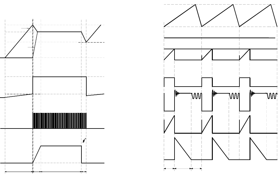
66
16.6 Operating description
The input voltage Vcc(pin 1) is monitored by a comparator with
hysteresis, enabling the circuit at 14.5V and disabling the
circuit below 7.5V. The error amplifier compares a voltage
Vfb(pin 14) related to the output voltage of the power supply,
with an internal 2.5V reference. The current sense comparator
compares the output of the error amplifier with the switch
current Isense(pin 7) of the power supply. The output of the
current sense comparator resets a latch, which is set every
cycle by the oscillator. The output stage is a totem pole,
capable of driving a MOSFET directly.
16.6.1 Start-up sequence
t1: Charging the capacitor at Vcc
C2129 will be charged via R3123 and R3134, C2133 and
C2111 via R3129. The output is switched off during t1.
t2: Charging of output capacitors
When the input voltage of the IC exceeds 14.5V, the circuit is
enabled and starts to produce output pulses. The current
consumption of the circuit increases to about 17mA, depending
on the external loads of the IC. At first, the capacitor at the Vcc
pin will discharge because the primary auxiliary voltage,
coming from winding 7-9 is below the Vcc voltage. At some
moment during t2, the primary auxiliary voltage reaches the
same level as Vcc. The Vcc voltage is now determinated by this
primary auxiliary voltage.
t3: regulation
The output voltage of the power supply is in regulation
t4: overload
When the output is shortened, the supply voltage of the circuit
will decrease and after some time drop below the lower
threshold voltage. At that moment, the output will be disabled
and the process of charging the Vcc capacitor starts again. If
the output is still shorted at the next t2 phase, the complete
start-and stop sequence will repeat. The power supply comes
in a hiccup mode
Figure 16-5 Start-up sequence
16.7 Regulation
Figure 16-6 shows the most relevant signals during the regulation
phase of the power supply.
The oscillator voltage ramps up and down between V1 and V2.
The voltage at the current sense terminal is compared every
cycle with the output of the error amplifier Vcomp. The output
is switched off when the current sense level exceeds the level
at the output of the error amplifier.
1. TimeON phase : A drain current will flow from the positive
supply at pin 1 of the transformer through the transformer's
primary winding, the MOSFET and Rsense to ground. As
the positive voltage at pin 1 of the transformer is constant,
the current will increase linearly and create a ramp
dependent on the mains voltage and the inductance of the
primary winding. A certain amount of energy is stored in the
transformer in the form of a magnetic field. The polarity of
the voltages at the secundary windings is such that the
diodes are non-conducting.
2. TimeDIODE phase : When the MOSFET is switched off,
energy is no longer supplied to the tranformer. The
inductance of the tranformer now tries to maintain the
current which has been flowing through it at a constant
level. The polarity of the voltage from the transformer
therefore becomes reversed. This results in a current flow
through the tranformer's secondary winding via the diodes,
electrolytic capacitors and the load. This current is also
ramp shaped but decreasing.
3. TimeDEAD phase : when the stored energy has been
supplied to the load, the current in the secondary windings
stops flowing. At this point the drain voltage of the
MOSFET will drop to the voltage of C2121 with a ringing
caused by the Drain-Source capacitance with the primary
inductance.
The oscillator will start a next cyclus which consists of the
described three phases. The time of the different phases
depends on the mains voltage and the load.
TimeDEAD is maximum at an input of 400VDC and minimum
load, it will be zero at an input of 100VDC and overload.
Figure 16-6 Regulation
1mA
Vo
0
OUTPUT
t4
short
Icc
0V
17mA
14.5V
7.5V
t1
Vcc
p.a.v.
t2 t3
10V
Vosc
Idiodes
Vgate
Vdrain
Idrain
Vsense
Vcomp
0
V2
V1
Ton Tdiode Tdead
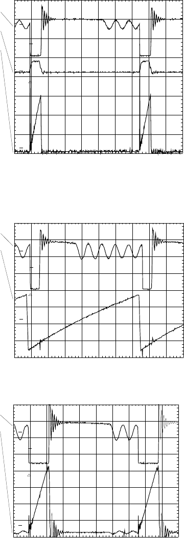
67
16.8 Oscillograms
Figure 16-7
PM3394B
ch2
ch3
ch1
CH1 2
CH2
CH3 2 V~ ALT MTB5.00us- 0.90dv ch1-
1
2
3
T
ch1 : Drain voltage
ch2 : Drain current
ch3 : Gate voltage
PM3394B
ch3
ch1
CH1 1
CH3 50mV~ ALT MTB5.00us- 0.90dv ch1-
1
3
T
ch1 : Drain voltage
ch2 : Oscillator voltage
PM3394B
ch3
ch1
CH1 1
CH3 20mV~ ALT MTB5.00us- 0.90dv ch1-
1
3
T
ch1 : Drain voltage
ch3 : Sense voltage
68
17. CIRCUIT DESCRIPTIONS AND ABBREVIATIONS
17.1 Input circuit
The input circuit consists of a lightning protection circuit and an
EMI filter.
The lightning protection comprises R3120, gasarrestor 1125
and R3124. The EMI filter is formed by C2120, L5120, C2125
and C2126. It prevents inflow of noises into the mains.
17.2 Primary rectifier/smoothing circuit
The AC input is rectified by rectifier bridge 6120 and smoothed
into C2121. The voltage over C2121 is approximately 300V. It
can vary from 100V to 390V.
17.3 Start circuit and Vcc supply
This circuit is formed by R3123, R3134, C2129, D6129, R3129,
R3111, C2133 and C2111.
When the power plug is connected to the mains voltage, the
stabilised voltage over D6129(24V) will charge C2133 via
R3129. When the voltage reaches 14.5V across C2111, the
control circuit of IC7110 is turned on and the regulation starts.
During regulation, Vcc of IC7110 will be supplied by the
rectified voltage from winding 7-9 via R3135, D6132 and
C2133.
17.4 Control circuit
The control circuit exists of IC7110, C2102, 2104, 2107, 2109,
2110, R3102, 3103, 3104, 3107, 3108, 3109 and 3110. The
frequency of the oscillator is defined by C2102 and R3110.
Power switch circuit
This circuit comprises MOSFET 7125, Rsense 3126, 3127 and
3128, R3125 , C2127, L5125, R3112 and R3113. R3125 is a
pull-down resistor to remove static charges from the gate of the
MOSFET.
17.5 Regulation circuit
The regulation circuit comprises opto-coupler 7200 which
isolates the error signal from the control IC on the primary side
and a reference component 7201. The TL431(7201) can be
represented by two components:
a very stable and accurate reference diode
a high gain amplifier
Figure 17-1
TL431 will conduct from cathode to anode when the reference
is higher than the internal reference voltage of about 2.5V. If the
reference voltage is lower, the cathode current is almost zero.
The cathode current flows through the LED of the opto-coupler.
The collector current of the opto-coupler flows through R3106,
producing an error voltage, connected to voltage feedback pin
14 of IC7110.
17.6 Demagnetisation
The auxiliary winding (7-9) voltage is used to detect magnetic
saturation of the transformer core and connected via R3101 to
pin 8 of IC7110. During the demagnetisation phase, the output
will be disabled.
17.7 Overvoltage protection circuit
This circuit consist of D6114, C2114, R3115 and R3116.
When the regulation circuit is interrupted due to an error in the
control loop, the regulated output voltage will increase
(overvoltage). This overvoltage is sensed on the primary
winding 7-9.
When an overvoltage longer than 2.0 (s is detected, the output
is disabled until VCC is removed and then re-applied. The
power supply will come in a hiccup mode as long as the error
in the control loop is present.
17.8 Secondary rectifier/smoothing circuit
There are 5 rectifier/smoothing circuits on the secondary side.
Each voltage depends on the number of windings of the
transformer.
The +5Vstby power supply is derived from the +12Vstby by
voltage regulator 7233, C2233 and L5233.
The -5V voltage is regulated by voltage regulator 7259 and will
be switched off via D6256, T7256 and T7255 during standby
(control signal STAND BY is high). When jumper 4250 is
mounted instead of this circuit, a supply voltage -8Vstby will be
present at pin 9 of connector 0205. -5V is used in DVD730 MK
II, DVD 930 MK II and DVD710. -8Vstby is used in DVD750 and
DVD950.
The +5V power supply is derived from +6Vstby by the loader-
up circuit formed by MOSFET 7236, reference component
7237, R3236, R3237 and C2239. This voltage will be switched
off during STAND BY via T7235.
The 3V3 power supply is regulated by the control loop (7201,
7200, 7110) of the switched mode PSU.
A
2.5V
R
K

69
17.9 List of abbreviations
B Buffered Video input Blue from DVD
monoboard
BC_AUX Blue or Chroma input from AUX-scart
BC_TV Blue or Chroma output to TV-scart
C_ENC Buffered Chroma input from DVD
monoboard
CVBS Buffered Composite video input from
DVD monoboard
DC_OFF Control signal to switch off 8Vstby
and +12Vstby during standby
DIG_OUT Digital out
FBIN_AUX Fast blanking input from AUX-scart
FBOUT_TV Fast blanking output to TV-scart
G Buffered Video input Green from DVD
monoboard
GIN_AUX Video input Green from AUX-scart
GOUT_TV Video output Green to TV-scart
HP_L Audio output left to headphone and
audio scart switch TEA6420
HP_R Audio output right to headphone and
audio scart switch TEA6420
KILL Kill control signal for audio outputs and
for soft mute of DAC
LIN_AUX Audio input left from AUX-scart
LIN_TV Audio input left from TV-scart
LOUT_AUX Audio output left to AUX-scart
LOUT_TV Audio output left to TV-scart
LRCLK Left/Right clock
PCM_CLK Audio system clock for DAC
PCM_OUT0 Audio serial output data
R Buffered Video input Red from DVD
monoboard
RCIN_TV Red or Chroma input from TV-scart
RCOUT_TV Red or Chroma output to TV-scart
RIN_AUX Audio input right from AUX-scart
RIN_TV Audio input right from TV-scart
ROUT_AUX Audio output right to AUX-scart
ROUT_TV Audio output right to TV-scart
SCL I2C bus clock
SCLK Audio serial bit clock
SDA I2C bus data
SELECT Control signal for video scart switches;
high = TV ,low = AUX
SELECT_HIGH Control signal for switching fast
blanking and slow blanking signals;
high = TV,.low = AUX
SLB_AUX Slow blanking control signal from
AUX-scart
SLB_TV Slow blanking control signal to TV-
scart
STANDBY Control signal from STI5505 used to
swith off 8Vstby and +12Vstby during
standby.
STEREO_L Audio cinch output left
STEREO_R Audio cinch output right
Y_ENC Buffered Luma input from DVD
monoboard
YCVBSIN_AUX Luma or CVBS input from AUX-scart
YCVBSIN_TV Luma or CVBS input from TV-scart
YCVBSOUT_AUX Luma or CVBS output to AUX-scart
YCVBSOUT_TV Luma or CVBS output to TV-scart
0/6/12 Scart switch control signal A/V board.
0V : loop through (AUX to TV), 6V :
play 16:9 format, 12V : play 4:3 format
ASSIGNMENT OF COMMON PARTS CODES.
RESISTORS
R 1) GD05 x x x 140, Carbon film fixed resistor, 5% 1/4W
R 2) GD05 x x x 160, Carbon film fixed resistor, 5% 1/6W
1 Resistance value
Examples
1 Resistance value
0.1 ..... 001 10 ......100 1k ...... 102 100k ...... 104
0.5 ..... 005 18 ......180 2.7k ...... 272 680k ...... 684
1 ..... 010 100 ......101 10k ...... 103 1M ...... 105
6.8 ..... 068 390 ......391 22k ......223 4.7M ...... 475
Note : Please distinguish 1/4W from 1/6W by the shape of parts
used actually.
CAPACITORS
C : CERAMIC CAP.
3) DD1 x x x x 370, Ceramic capacitor
Disc type
Temp.coeff. P350~N1000, 50V
3 Capacity value
2 Tolerance
Examples
2 Tolerance (Capacity deviation)
0.25 pF ....... 0
0.5 pF ....... 1
5 % ....... 5
Tolerance of COMMON PARTS handled here are as follows :
0.5 pF - 5 pF ....... 0.25 pF
6 pF - 10 pF ..... 0.5 pF
12 pF - 560 pF ... 5 %
3 Capacity value
0.5 pF .... 005 3 pF ..... 030 100 pF ..... 101
1 pF .... 010 10 pF ..... 100 220 pF ..... 221
1.5 pF .... 015 47 pF ..... 470 560 pF..... 561
C : CERAMIC CAP.
4) DK16 x x x 300, High dielectric constant ceramic
capacitor
Disc type
Temp.chara. 2B4, 50V
4 Capacity value
Examples
4 Capacity value
100 pF ..... 101 1000 pF .... 102 10000 pF .... 103
470 pF ..... 471 2200 pF .... 222
C : 5) ELECTROLY CAP.( ), 6)FILM CAP ( )
5) EA x x x x x x 10, Electrolytic capacitor
One-way lead type,Tolerance 20%
6 Working voltage
5 Capacity value
Examples
5 Capacity value
0.1 F .... 104 4.7 F .... 475 100 F ..... 107
0.33 F .... 334 10 F .... 106 330 F .....337
1 F .... 105 22 F .... 226 1100 F ..... 118
2200 F .... 228
6 Working voltage
6.3 V ...... 006 25 V ..... 025
10 V ...... 010 35 V ..... 035
16 V ...... 016 50 V ..... 050
6) DF15 x x x 350 Plastic film capacitor
DF15 x x x 310 One-way type, Mylar 5% 50V
DF16 x x x 310 Plastic film capacitor
One-way type, Mylar 10% 50V
7 Capacity value
Examples
7 Capacity value
0.001 F (1000 pF) ...... 102 0.1 F...... 104
0.0018 F........................ 182 0.56 F...... 564
0.01 F........................ 103 1 F ......105
0.015 F........................ 153
1) The above CODES(R ,R ,C ,C
and C ) are omitted on the schematic diagram in
some case.
2) On the occasion, be confirmed the common parts on the
parts list.
3) Refer to “Common Parts List” for the other common
parts(Rl05, DD4, DK4).
NOTE
NOTE ON SAFETY:
Symbol Fire or electrical shock hazard. Only original
parts should be used to replaced any part marked with
symbol Any other component substitution ( other than
original type), may increase risk of fire or electrical shock
hazard.
990521 A.O
NOTE ON SAFETY FOR FUSIBLE RESIST OR :
The suppliers and their type numbers of fusible resistors are as
follows ;
1 . KOA Corporation
Part No.(MJI) Type No.(KOA) Description
NH05 x x x 140 RF25S x x x x J
J
J
J
5% (1/4W)
NH05 x x x 120 RF50S x x x x 5% (1/2W)
NH85 x x x 110 RF73B2A x x x x 5% (1/10W)
NH95 x x x 140 RF73B2E x x x x 5% (1/4W)
Resistance value Resistance value(0.1 - 10k )
2. Matsushita Electronic Components Co., Ltd
Part No.(MJI) Type No.(MEC) Description
NF05 x x x 140 ERD-2FCJ x x x ( 5% 1/4W)
RF05 x x x 140
NF02 x x x 140 ERD-2FCG x x x ( 2% 1/4W)
RF02 x x x 140
Resistance value
Examples
Resistance value
0.1 ..... 001 10 ..... 100 1k ..... 102 100k ..... 104
0.5 ..... 005 18 ..... 180 2.7k ..... 272 680k ..... 684
1 ..... 010 100 ..... 101 10k ..... 103 1M ..... 105
6.8 ..... 068 390 ..... 391 22k ..... 223 4.7M ..... 475
ABBREVIA
TION AND MARKS
ANT. : ANTENNA BATT. : BATTERY
CAP. : CAPACITOR CER. : CERAMIC
CONN. : CONNECTING DIG. : DIGITAL
HP : HEADPHONE MIC. : MICROPHONE
-PRO : MICROPROCESSOR REC. : RECORDING
RES. : RESISTOR SPK : SPEAKER
SW : SWITCH TRANSF. : TRANSFORMER
TRIM. : TRIMMING TRS. : TRANSISTOR
VAR. : VARIABLE X’ TAL : CRYSTAL
:
:
70
18. ELECTRICAL PARTS LIST
71
POS.
NO VERS.
COLOR PART NO.
(PCS) DESCRIPTION PART NO.
(MJI) POS.
NO VERS.
COLOR PART NO.
(PCS) DESCRIPTION PART NO.
(MJI)
AV CIRCUIT BOARD
(/A1B,/S1G,/U1B)
CAPACITORS
2000 3198 028 41090 ELECT 10 F 20% 35V QT02841090
2001 4822 126 13838 CER. 100NF 50V QP12613838
2002 4822 126 13692 CER. 47pF 1% 63V QP12613692
2004 4822 126 13692 CER. 47pF 1% 63V QP12613692
2006 4822 124 41796 ELECT 22 F 20% 16V QP12441796
2007 4822 124 23432 ELECT 100 F 20% 10V QP12423432
2029 4822 124 81286 ELECT 47 F 20% 16V QP12481286
2030 4822 126 13482 CER. 470NF +80 -20% 16V QP12613482
2032 4822 126 13482 CER. 470NF +80 -20% 16V QP12613482
2033 4822 122 33575 CER. 220pF 5% 63V QP12233575
2036 4822 124 41643 ELECT 100 F 20% 16V QP12441643
2038 4822 124 41584 ELECT 100 F 20% 10V QP12441584
2039 4822 124 40181 ELECT 220 F 20% 10V QP12440181
2040 4822 124 41643 ELECT 100 F 20% 16V QP12441643
2041 4822 124 41643 ELECT 100 F 20% 16V QP12441643
2100 5322 122 32654 CER. 22N 63V QQ12232654
2101 5322 122 32531 CER. 100pF 5% 50V QQ12232531
2104 5322 122 31647 CER. 1NF 10% 63V QQ12231647
2106 5322 122 32531 CER. 100pF 5% 50V QQ12232531
2107 5322 122 32531 CER. 100pF 5% 50V QQ12232531
2108 5322 122 32654 CER. 22N 63V QQ12232654
2109 4822 126 13838 CER. 100NF 50V QP12613838
2110 4822 124 81286 ELECT 47 F 20% 16V QP12481286
2113 5322 122 31647 CER. 1NF 10% 63V QQ12231647
2115 5322 122 32531 CER. 100pF 5% 50V QQ12232531
2119 5322 122 31647 CER. 1NF 10% 63V QQ12231647
2121 5322 122 31647 CER. 1NF 10% 63V QQ12231647
2123 4822 122 33575 CER. 220pF 5% 63V QP12233575
2124 4822 126 14585 CER. 100NF 10% 50V QP12614585
2125 5322 122 32654 CER. 22N 3V QQ12232654
2126 5322 122 32654 CER. 22N 63V QQ12232654
2130 5322 122 32654 CER. 22N 63V QQ12232654
2131 5322 122 32654 CER. 22N 63V QQ12232654
2132 4822 124 22339 ELECT 100 E 16V QP12422339
2133 4822 124 22339 ELECT 100 E 16V QP12422339
2134 4822 124 11947 ELECT 10 F 20% 16V QP12411947
DIODES
6001 4822 130 11087 DIODE BZX284-C15 QP13011087
6006
6007 4822 130 83757 DIODE BAS216 QP13083757
6008 4822 130 83757 DIODE BAS216 QP13083757
6009 4822 130 83757 DIODE BAS216 QP13083757
6010 4822 130 11087 DIODE BZX284-C15 QP13011087
SEMICONDUCTORS
7103 4822 209 17423 IC ANA UAD1328T QP20917423
7110 4822 209 16978 IC ANA LF33CV QP20916978
7115 4822 209 30095 IC ANA LM833D QP20930095
7116 9322 141 80668 IC ANA AD8073
7117 4822 209 72684 IC ANA L7905CV QP20972684
7000 5322 130 60159 TRS. BC846B QQ13060159
7001 4822 130 42804 TRS. BC817-25 QP13042804
7002 4822 130 60373 TRS. BC856B QP13060373
7004 4822 130 42804 TRS. BC817-25 QP13042804
7005 4822 130 42804 TRS. BC817-25 QP13042804
7006 5322 130 60159 TRS. BC846B QQ13060159
7007 5322 130 60159 TRS. BC846B QQ13060159
7008 5322 130 60159 TRS. BC846B QQ13060159
7009 4822 130 60373 TRS. BC856B QP13060373
7010 5322 130 60159 TRS. BC846B QQ13060159
7011 5322 130 60159 TRS. BC846B QQ13060159
7012 4822 130 60373 TRS. BC856B QP13060373
7013 5322 130 60159 TRS. BC846B QQ13060159
7014 5322 130 60159 TRS. BC846B QQ13060159
7015 4822 130 60373 TRS. BC856B QP13060373
7016 5322 130 60159 TRS. BC846B QQ13060159
7017 5322 130 60159 TRS. BC846B QQ13060159
7018 5322 130 60159 TRS. BC846B QQ13060159
7019 5322 130 60159 TRS. BC846B QQ13060159
7104 4822 130 42804 TRS. BC817-25 QP13042804
7105 4822 130 42804 TRS. BC817-25 QP13042804
7108 4822 130 42804 TRS. BC817-25 QP13042804
7109 4822 130 42804 TRS. BC817-25 QP13042804
7112 4822 130 42804 TRS. BC817-25 QP13042804
7114 4822 130 42804 TRS. BC817-25 QP13042804
RESISTORS
3000 4822 051 20101 100R00 5% 0.1W QP05120101
3001 4822 117 12521 68R 1% 0.1W QP11712521
3005 4822 051 20472 4K70 5% 0.1W QP05120472
3006 4822 051 20472 4K70 5% 0.1W QP05120472
3007 4822 117 12955 2K7 1% 0.1W QP11712955
3008 4822 117 10833 10k 1% 0.1W QP11710833
3009 4822 051 20472 4K70 5% 0.1W QP05120472
3010 4822 051 20472 4K70 5% 0.1W QP05120472
3011 4822 051 20472 4K70 5% 0.1W QP05120472
3012 4822 117 11152 4R7 5% QP11711152
3014 4822 051 20101 100R00 5% 0.1W QP05120101
3015 4822 117 12955 2K7 1% 0.1W QP11712955
3016 4822 051 20101 100R00 5% 0.1W QP05120101
3017 4822 117 12955 2K7 1% 0.1W QP11712955
3036 4822 117 11449 2K2 5% 0.1W QP11711449
3038 4822 051 20223 22K00 5% 0.1W QP05120223
3039 4822 051 20223 22K00 5% 0.1W QP05120223
3040 4822 116 83933 15K 1% 0.1W QP11683933
3041 4822 051 20822 8K20 5% 0.1W QP05120822
3043 4822 117 11504 270R 1% 0.1W QP11711504
3044 4822 117 10833 10k 1% 0.1W QP11710833
3045 4822 051 20101 100R00 5% 0.1W QP05120101
3046 4822 051 20101 100R00 5% 0.1W QP05120101
3047 4822 117 11507 6K8 1% 0.1W QP11711507
3048 4822 117 11454 820R 1% 0.1W QP11711454
3049 4822 117 11927 75R 1% 0.1W QP11711927
3050 4822 051 20471 470R00 5% 0.1W QP05120471
3051 4822 051 20472 4K70 5% 0.1W QP05120472
3052 4822 117 10361 680R 1% 0.1W QP11710361
3056 4822 117 11504 270R 1% 0.1W QP11711504
3057 4822 117 11152 4R7 5% QP11711152
3058 4822 051 20101 100R00 5% 0.1W QP05120101
3059 4822 051 20101 100R00 5% 0.1W QP05120101
3060 4822 117 11507 6K8 1% 0.1W QP11711507
3061 4822 117 11454 820R 1% 0.1W QP11711454
3062 4822 117 11927 75R 1% 0.1W QP11711927
3063 4822 117 11449 2K2 5% 0.1W QP11711449
3064 4822 051 20472 4K70 5% 0.1W QP05120472
3065 4822 117 10361 680R 1% 0.1W QP11710361
3068 4822 117 11504 270R 1% 0.1W QP11711504
3069 4822 051 20101 100R00 5% 0.1W QP05120101
3070 4822 117 11507 6K8 1% 0.1W QP11711507
3071 4822 117 11454 820R 1% 0.1W QP11711454
3072 4822 117 11927 75R 1% 0.1W QP11711927
3073 4822 117 11449 2K2 5% 0.1W QP11711449
3074 4822 051 20472 4K70 5% 0.1W QP05120472
3075 4822 117 10361 680R 1% 0.1W QP11710361
3077 4822 117 11927 75R 1% 0.1W QP11711927
3078 4822 117 11449 2K2 5% 0.1W QP11711449
3100 4822 051 20101 100R00 5% 0.1W QP05120101
3101 4822 051 20472 4K70 5% 0.1W QP05120472
3102 4822 117 10833 10k 1% 0.1W QP11710833
72
POS.
NO VERS.
COLOR PART NO.
(PCS) DESCRIPTION PART NO.
(MJI) POS.
NO VERS.
COLOR PART NO.
(PCS) DESCRIPTION PART NO.
(MJI)
3103 4822 117 10833 10k 1% 0.1W QP11710833
3105 4822 117 10833 10k 1% 0.1W QP11710833
3106 4822 117 10833 10k 1% 0.1W QP11710833
3107 4822 051 20101 100R00 5% 0.1W QP05120101
3108 4822 117 11152 4R7 5% QP11711152
3109 4822 117 11152 4R7 5% QP11711152
3110 4822 117 10833 10k 1% 0.1W QP11710833
3112 4822 117 12955 2K7 1% 0.1W QP11712955
3113 4822 117 12955 2K7 1% 0.1W QP11712955
3114 4822 117 10833 10k 1% 0.1W QP11710833
3117
3118 4822 051 20101 100R00 5% 0.1W QP05120101
3119 4822 051 20101 100R00 5% 0.1W QP05120101
3120 4822 117 10833 10k 1% 0.1W QP11710833
3121 4822 117 10833 10k 1% 0.1W QP11710833
3122 4822 117 12955 2K7 1% 0.1W QP11712955
3123 4822 117 12955 2K7 1% 0.1W QP11712955
3124 4822 117 10833 10k 1% 0.1W QP11710833
3126 4822 051 20101 100R00 5% 0.1W QP05120101
3127 4822 117 10833 10k 1% 0.1W QP11710833
3129 4822 117 12955 2K7 1% 0.1W QP11712955
3130 4822 051 20101 100R00 5% 0.1W QP05120101
3131 4822 117 10833 10k 1% 0.1W QP11710833
3132 4822 117 12955 2K7 1% 0.1W QP11712955
3135 5322 117 12487 1k 1% 0.125W RC12G QQ11712487
3136 5322 117 12487 1k 1% 0.125W RC12G QQ11712487
3137 4822 117 12635 10R 1% 0.125W QP11712635
3138 4822 117 11139 1k5 1% 0.1W QP11711139
3139 4822 117 11931 750R 1% 0.1W QP11711931
3140 2120 108 92619 SM ERJ6EN 2K2PM1
3141 5322 117 12487 1k 1% 0.125W RC12G QQ11712487
3142 5322 117 12487 1k 1% 0.125W RC12G QQ11712487
3143 5322 117 12487 1k 1% 0.125W RC12G QQ11712487
3144 4822 117 11953 560R 1% 0.1W QP11711953
3145 2120 108 92625 SM ERJ6EN 5K6PM1
3147 2120 108 92616 SM ERJ6EN 1k2 PM1
3148 5322 117 12487 1k 1% 0.125W RC12G QQ11712487
3150 4822 117 11927 75R 1% 0.1W QP11711927
3153 4822 051 20101 100R00 5% 0.1W QP05120101
3154 4822 117 11927 75R 1% 0.1W QP11711927
3157 4822 117 11927 75R 1% 0.1W QP11711927
3158 4822 117 11449 2K2 5% 0.1W QP11711449
3159 4822 051 20101 100R00 5% 0.1W QP05120101
3160 4822 117 10833 10k 1% 0.1W QP11710833
MISCELLANEOUS
1002 2422 026 05047 CONNECTOR CINCH H 6P
F RDWHYE B QU02605047
1003 4822 267 10994 CONNECTOR 4P MDIN QP26710994
1004 2422 025 16526 CONNECTOR 22P F 1.00
FFC 0.3 R QU02516526
1005 4822 267 31729 CONNECTOR QP26731729
1006 2422 026 05049 CON BM CINCH H 3P F QU02605049
1007 2422 025 16525 CONNECTOR 16P F 1.00
FFC 0.3 R QU02516525
5000 4822 157 70601 COIL 100UH (920927085A) QP15770601
5003
5007 4822 242 10756 FILTER L/C
DSS306-92Y5S221M100 QP24210756
7020 9322 155 28667 CONNECTOR
GP1FA550TZ (SRPJ)L
AV CIRCUIT BOARD (/N1B)
CAPACITORS
2032 4822 126 13482 CER. 470NF +80 -20% 16V QP12613482
2353 4822 124 40769 ELECT 4.7 F 20% 100V QP12440769
2354 4822 126 14076 CER. 220N 25V QP12614076
2355 4822 124 40769 ELECT 4.7 F 20% 100V QP12440769
2357 4822 124 40769 ELECT 4.7 F 20% 100V QP12440769
2358 4822 122 33575 CER. 220pF 5% 63V QP12233575
2359 4822 124 40769 ELECT 4.7 F 20% 100V QP12440769
2360 4822 126 13692 CER. 47pF 1% 63V QP12613692
2361 4822 126 13692 CER. 47pF 1% 63V QP12613692
2371 4822 122 33575 CER. 220pF 5% 63V QP12233575
2372 4822 124 40769 ELECT 4.7 F 20% 100V QP12440769
2373 4822 124 40769 ELECT 4.7 F 20% 100V QP12440769
2377 4822 122 33575 CER. 220pF 5% 63V QP12233575
2378 4822 124 40769 ELECT 4.7 F 20% 100V QP12440769
2382 4822 124 40769 ELECT 4.7 F 20% 100V QP12440769
2383 4822 124 40769 ELECT 4.7 F 20% 100V QP12440769
2385 4822 124 40769 ELECT 4.7 F 20% 100V QP12440769
2395 4822 122 33575 CER. 220pF 5% 63V QP12233575
2402 4822 122 33575 CER. 220pF 5% 63V QP12233575
2404 4822 122 33575 CER. 220pF 5% 63V QP12233575
2408 4822 122 33575 CER. 220pF 5% 63V QP12233575
2409 4822 122 33575 CER. 220pF 5% 63V QP12233575
2412 4822 124 40433 ELECT 47 F 20% 25V QP12440433
2450 5322 122 32654 CER. 22N 63V QQ12232654
2452 4822 126 14076 CER. 220N 25V QP12614076
2453 4822 124 40433 ELECT 47 F 20% 25V QP12440433
2455 5322 122 32531 CER. 100pF 5% 50V QQ12232531
2456 4822 124 22339 ELECT 100 E 16V QP12422339
2457 5322 126 10511 CER. 1NF 5% 50V QQ12610511
2458 5322 122 32654 CER. 22N 63V QQ12232654
2459 5322 122 32531 CER. 100pF 5% 50V QQ12232531
2460 5322 122 32654 CER. 22N 63V QQ12232654
2461 5322 122 32531 CER. 100pF 5% 50V QQ12232531
2462 4822 124 22339 ELECT 100 E 16V QP12422339
2463 5322 126 10511 CER. 1NF 5% 50V QQ12610511
2464 5322 122 32531 CER. 100pF 5% 50V QQ12232531
2469 5322 122 32654 CER. 22N 63V QQ12232654
2471 4822 126 14585 CER. 100NF 10% 50V QP12614585
2472 4822 124 40433 ELECT 47 F 20% 25V QP12440433
2488 4822 126 14585 CER. 100NF 10% 50V QP12614585
2495 4822 126 14585 CER. 100NF 10% 50V QP12614585
2496 5322 122 32654 CER. 22N 63V QQ12232654
2497 4822 124 81151 ELECT 22 F 50V QP12481151
2498 4822 124 41584 ELECT 100 F 20% 10V QP12441584
2499 4822 122 33575 CER. 220pF 5% 63V QP12233575
2505
2506 4822 124 40763 ELECT 2.2 F 100V QP12440763
2509
2511 4822 124 40763 ELECT 2.2 F 100V QP12440763
2520 4822 122 33575 CER. 220pF 5% 63V QP12233575
2523
2527 5322 122 32654 CER. 22N 63V QQ12232654
2537
2538 4822 124 40763 ELECT 2.2 F 100V QP12440763
2539 4822 124 40763 ELECT 2.2 F 100V QP12440763
2540 4822 124 40763 ELECT 2.2 F 100V QP12440763
2541 4822 126 14585 CER. 100NF 10% 50V QP12614585
2542 4822 126 14491 CER. 2.2 F 10V QP12614491
2543 4822 126 13692 CER. 47pF 1% 63V QP12613692
2544 4822 124 40248 ELECT 10 F 20% 63V QP12440248
2545 4822 124 40433 ELECT 47 F 20% 25V QP12440433

73
POS.
NO VERS.
COLOR PART NO.
(PCS) DESCRIPTION PART NO.
(MJI) POS.
NO VERS.
COLOR PART NO.
(PCS) DESCRIPTION PART NO.
(MJI)
DIODES
6302 4822 130 83757 DIODE BAS216 QP13083757
6401 4822 130 11047 DIODE BZX284-C9V1 QP13011047
6403 4822 130 83757 DIODE BAS216 QP13083757
6404 4822 130 11383 DIODE BZX284-C5V1 QP13011383
SEMICONDUCTORS
7400 9322 134 92676 IC ANA L78L33
7401 4822 209 17423 IC ANA UAD1328T QP20917423
7403 4822 209 32071 IC ANA MC33079D QP20932071
7900 5322 209 14481 IC DIG HEF4053BT QQ20914481
7905
7917 4822 209 17512 IC ANA TEA6420D QP20917512
7006 5322 130 60159 TRS. BC846B QQ13060159
7007 5322 130 60159 TRS. BC846B QQ13060159
7008 5322 130 60159 TRS. BC846B QQ13060159
7009 4822 130 60373 TRS. BC856B QP13060373
7010 5322 130 60159 TRS. BC846B QQ13060159
7014
7300 4822 130 60373 TRS. BC856B QP13060373
7301 5322 130 60159 TRS. BC846B QQ13060159
7304 9322 134 86668 TRS. LF80C
7310 5322 130 60159 TRS. BC846B QQ13060159
7329 5322 130 60159 TRS. BC846B QQ13060159
7330 5322 130 60159 TRS. BC846B QQ13060159
7331 4822 130 40959 TRS. BC547B QP13040959
7332 4822 130 60373 TRS. BC856B QP13060373
7333 4822 130 41246 TRS. BC327-25 QP13041246
7334 5322 130 60159 TRS. BC846B QQ13060159
7335 5322 130 60159 TRS. BC846B QQ13060159
7402 4822 130 42804 TRS. BC817-25 QP13042804
7404 4822 130 42615 TRS. BC817-40 QP13042615
7407
7918 5322 130 60159 TRS. BC846B QQ13060159
7935
7936 4822 130 60373 TRS. BC856B QP13060373
7939
7941 4822 130 60373 TRS. BC856B QP13060373
7942 4822 130 60373 TRS. BC856B QP13060373
7943 5322 130 60159 TRS. BC846B QQ13060159
7944 5322 130 60159 TRS. BC846B QQ13060159
7945 4822 130 60373 TRS. BC856B QP13060373
7946 4822 130 60373 TRS. BC856B QP13060373
7947 5322 130 60159 TRS. BC846B QQ13060159
7949 5322 130 60159 TRS. BC846B QQ13060159
RESISTORS
3036 4822 117 11449 2K2 5% 0.1W QP11711449
3038 4822 051 20223 22K00 5% 0.1W QP05120223
3039 4822 117 10834 47k 1% 0.1W QP11710834
3040 4822 051 20273 27K00 5% 0.1W QP05120273
3041 4822 051 20822 8K20 5% 0.1W QP05120822
3043 4822 117 13577 330R 1% 1.25W QP11713577
3044 4822 051 20223 22K00 5% 0.1W QP05120223
3045 4822 051 20101 100R00 5% 0.1W QP05120101
3046 4822 051 20101 100R00 5% 0.1W QP05120101
3049 4822 117 11927 75R 1% 0.1W QP11711927
3050 4822 117 11503 220R 1% 0.1W QP11711503
3056 4822 117 13577 330R 1% 1.25W QP11713577
3058 4822 051 20101 100R00 5% 0.1W QP05120101
3059 4822 051 20101 100R00 5% 0.1W QP05120101
3062 4822 117 11927 75R 1% 0.1W QP11711927
3063 4822 051 10102 1K00 2% 0.25W QP05110102
3300 4822 117 13577 330R 1% 1.25W QP11713577
3301 4822 051 20101 100R00 5% 0.1W QP05120101
3313 4822 117 11503 220R 1% 0.1W QP11711503
3314 4822 051 10102 1K00 2% 0.25W QP05110102
3315 4822 051 20471 470R00 5% 0.1W QP05120471
3316 4822 117 10834 47k 1% 0.1W QP11710834
3318 4822 117 10834 47k 1% 0.1W QP11710834
3319 4822 051 10102 1K00 2% 0.25W QP05110102
3320 4822 117 10834 47k 1% 0.1W QP11710834
3321 4822 051 20101 100R00 5% 0.1W QP05120101
3322 4822 051 20101 100R00 5% 0.1W QP05120101
3323 4822 051 20471 470R00 5% 0.1W QP05120471
3325 4822 117 10834 47k 1% 0.1W QP11710834
3339 4822 051 10102 1K00 2% 0.25W QP05110102
3340 4822 051 10102 1K00 2% 0.25W QP05110102
3343 4822 117 11927 75R 1% 0.1W QP11711927
3345 4822 117 11927 75R 1% 0.1W QP11711927
3347 4822 051 10102 1K00 2% 0.25W QP05110102
3348 4822 051 10102 1K00 2% 0.25W QP05110102
3349 4822 117 10834 47k 1% 0.1W QP11710834
3351 4822 051 20471 470R00 5% 0.1W QP05120471
3359 4822 117 10834 47k 1% 0.1W QP11710834
3363 4822 051 10102 1K00 2% 0.25W QP05110102
3366 4822 117 10834 47k 1% 0.1W QP11710834
3394 4822 051 20471 470R00 5% 0.1W QP05120471
3397 4822 117 10834 47k 1% 0.1W QP11710834
3407 4822 117 11927 75R 1% 0.1W QP11711927
3408 4822 117 11927 75R 1% 0.1W QP11711927
3409 4822 117 11503 220R 1% 0.1W QP11711503
3413 4822 117 10834 47k 1% 0.1W QP11710834
3425 4822 117 11927 75R 1% 0.1W QP11711927
3432 4822 117 11927 75R 1% 0.1W QP11711927
3442 4822 051 20101 100R00 5% 0.1W QP05120101
3444 4822 117 10833 10k 1% 0.1W QP11710833
3445 4822 117 10833 10k 1% 0.1W QP11710833
3446 4822 117 12955 2K7 1% 0.1W QP11712955
3447 4822 117 12955 2K7 1% 0.1W QP11712955
3448 4822 117 10833 10k 1% 0.1W QP11710833
3451 4822 117 10833 10k 1% 0.1W QP11710833
3453 4822 117 10833 10k 1% 0.1W QP11710833
3454 4822 117 10833 10k 1% 0.1W QP11710833
3455 4822 117 10833 10k 1% 0.1W QP11710833
3457 4822 051 20101 100R00 5% 0.1W QP05120101
3459 4822 117 10833 10k 1% 0.1W QP11710833
3461 4822 117 10833 10k 1% 0.1W QP11710833
3462 4822 117 12955 2K7 1% 0.1W QP11712955
3463 4822 117 12955 2K7 1% 0.1W QP11712955
3464 4822 117 10833 10k 1% 0.1W QP11710833
3505 4822 051 20101 100R00 5% 0.1W QP05120101
3507 4822 051 20101 100R00 5% 0.1W QP05120101
3508 4822 117 12521 68R 1% 0.1W QP11712521
3511 4822 117 10833 10k 1% 0.1W QP11710833
3512 4822 117 10833 10k 1% 0.1W QP11710833
3517 4822 051 20101 100R00 5% 0.1W QP05120101
3519 4822 051 20562 5K6 5% 0.1W QP05120562
3610 4822 051 20472 4K70 5% 0.1W QP05120472
3611 4822 051 20472 4K70 5% 0.1W QP05120472
3612 4822 117 10834 47k 1% 0.1W QP11710834
3613 4822 117 12955 2K7 1% 0.1W QP11712955
3614 4822 051 20223 22K00 5% 0.1W QP05120223
3615 4822 117 11152 4R7 5% QP11711152
3616 4822 051 20472 4K70 5% 0.1W QP05120472
3617 4822 117 10833 10k 1% 0.1W QP11710833
3618 4822 051 10102 1K00 2% 0.25W QP05110102
3619 4822 117 10833 10k 1% 0.1W QP11710833
3620 4822 051 10008 0R00 5% 0.25W QP05110008
3621 4822 051 20472 4K70 5% 0.1W QP05120472

74
POS.
NO VERS.
COLOR PART NO.
(PCS) DESCRIPTION PART NO.
(MJI) POS.
NO VERS.
COLOR PART NO.
(PCS) DESCRIPTION PART NO.
(MJI)
3622 4822 117 10833 10k 1% 0.1W QP11710833
3623 4822 051 20472 4K70 5% 0.1W QP05120472
3624 4822 117 10833 10k 1% 0.1W QP11710833
3625 4822 051 10102 1K00 2% 0.25W QP05110102
3629 4822 117 11927 75R 1% 0.1W QP11711927
3632 4822 051 20101 100R00 5% 0.1W QP05120101
3634 4822 117 11449 2K2 5% 0.1W QP11711449
3635 4822 117 11503 220R 1% 0.1W QP11711503
3636 4822 117 10837 100k 1% 0.1W QP11710837
3643
3646 4822 117 10837 100k 1% 0.1W QP11710837
3647 4822 117 10837 100k 1% 0.1W QP11710837
3648 4822 117 13577 330R 1% 1.25W QP11713577
3651
3653 4822 117 13577 330R 1% 1.25W QP11713577
3672 4822 117 11927 75R 1% 0.1W QP11711927
3675
3676 4822 117 10353 150R 1% 0.1W QP11710353
3677 4822 117 11927 75R 1% 0.1W QP11711927
3678 4822 051 20101 100R00 5% 0.1W QP05120101
3685
3687 4822 051 20472 4K70 5% 0.1W QP05120472
3688 4822 051 20101 100R00 5% 0.1W QP05120101
3689 4822 051 20101 100R00 5% 0.1W QP05120101
3690 4822 051 10102 1K00 2% 0.25W QP05110102
3694
3695 4822 117 10833 10k 1% 0.1W QP11710833
3696 4822 117 10833 10k 1% 0.1W QP11710833
3697 4822 051 10102 1K00 2% 0.25W QP05110102
3700
3701 4822 051 20471 470R00 5% 0.1W QP05120471
3702 4822 051 10102 1K00 2% 0.25W QP05110102
3703 4822 117 11507 6K8 1% 0.1W QP11711507
3707
3720 4822 117 11148 56K 1% 0.1W QP11711148
3721 4822 117 10353 150R 1% 0.1W QP11710353
3722 4822 117 11148 56K 1% 0.1W QP11711148
3723 4822 117 11148 56K 1% 0.1W QP11711148
3724 4822 051 20229 22R00 5% 0.1W QP05120229
3731
3732 4822 117 13577 330R 1% 1.25W QP11713577
3747
3748 4822 117 10837 100k 1% 0.1W QP11710837
3761
3762 4822 117 11504 270R 1% 0.1W QP11711504
3763 4822 051 20101 100R00 5% 0.1W QP05120101
3764 4822 117 10833 10k 1% 0.1W QP11710833
3765 4822 117 10833 10k 1% 0.1W QP11710833
3768 4822 117 10834 47k 1% 0.1W QP11710834
3772
3773 4822 117 10833 10k 1% 0.1W QP11710833
3774 4822 117 10834 47k 1% 0.1W QP11710834
3800 4822 051 20472 4K70 5% 0.1W QP05120472
3801 4822 051 20472 4K70 5% 0.1W QP05120472
!3802 4822 117 11152 4R7 5% QP11711152
!3803 4822 117 11152 4R7 5% QP11711152
3804 4822 117 10834 47k 1% 0.1W QP11710834
3805 4822 117 10833 10k 1% 0.1W QP11710833
3999 4822 117 12842 QP11712842
MISCELLANEOUS
1300 4822 265 11154 CONNECTOR
52030-2210 (22P) QP26511154
1301 4822 265 11103 CONNECTOR
52030-1610 (16P) QP26511103
1303 4822 267 10994 CONNECTOR 4P MDIN QP26710994
1304 2422 033 00334 CON BM EURO H 42P F
BK GRND-L QU03300334
1402 4822 265 11566 CONNECTOR 3P YKC21-3930 QP26511566
1405 4822 267 31729 CONNECTOR QP26731729
1410 4822 265 41392 CONNECTOR B7B-EH-A QP26541392
5400 4822 157 70601 COIL 100µH (920927085A) QP15770601
6400 4822 130 10845 CONNECTOR GP1F32T QP13010845
FRONT CIRCUIT BOARD
CAPACITORS
2100 /N1B 4822 122 33575 CER. 220pF 5% 63V QP12233575
2101 /N1B 4822 122 33575 CER. 220pF 5% 63V QP12233575
2102 5322 122 32531 CER. 100pF 5% 50V QQ12232531
2103 5322 122 32531 CER. 100pF 5% 50V QQ12232531
2105 4822 126 12105 CER. 33NF 50V QP12612105
2106 4822 124 40248 ELECT 10µF 20% 63V QP12440248
2107 4822 126 12105 CER. 33NF 50V QP12612105
2111
2114 5322 122 32658 CER. 22pF 5% 50V QQ12232658
2115 5322 122 32658 CER. 22pF 5% 50V QQ12232658
2116 4822 126 12105 CER. 33NF 50V QP12612105
2117 4822 124 40248 ELECT 10µF 20% 63V QP12440248
2122 4822 126 12105 CER. 33NF 50V QP12612105
2123 4822 124 11947 ELECT 10µF 20% 16V QP12411947
2124 3198 028 42290 ELECT 22µF 35V
2125 5322 122 32658 CER. 22pF 5% 50V QQ12232658
2126 4822 124 40248 ELECT 10µF 20% 63V QP12440248
2128 5322 122 31647 CER. 1NF 10% 63V QQ12231647
2129 3198 028 42290 ELECT 22µF 35V
2130 3198 028 42290 ELECT 22µF 35V
2201 4822 126 12105 CER. 33NF 50V QP12612105
2211 5322 122 32531 CER. 100pF 5% 50V QQ12232531
DIODES
6100 /N1B 4822 130 83757 DIODE BAS216 QP13083757
6101 4822 130 11666 DIODE BZX284-C8V2 QP13011666
6102 4822 130 10794 DIODE BZX284-C10 QP13010794
6104 4822 130 83757 DIODE BAS216 QP13083757
6200 4822 130 82978 LED LTL-16KPE-P QP13082978
SEMICONDUCTORS
7104 /N1B 3104 123 94532 IC DIG TMP87CH74F-1E29-V2.
18-DVDSLAVE QW12394532
7104
/A1B,
/S1G,/U1B
3104 123 94761 IC DIG ROM TMP87CH74 QW12394761
7112 4822 209 31257 IC ANA MC79L24ACP QP20931257
7100 5322 130 60159 TRS. BC846B QQ13060159
7101 /N1B 5322 130 60159 TRS. BC846B QQ13060159
7102 5322 130 60159 TRS. BC846B QQ13060159
7103 5322 130 60159 TRS. BC846B QQ13060159
7105 4822 130 40855 TRS. BC337 QP13040855
7106 4822 130 40854 TRS. BC327 QP13040854
7107 5322 130 60159 TRS. BC846B QQ13060159
7108 5322 130 60159 TRS. BC846B QQ13060159
7109 4822 130 60373 TRS. BC856B QP13060373
7110 4822 212 30842 REMOTE RECEIVER
TSOP1736SB1 QP21230842

75
POS.
NO VERS.
COLOR PART NO.
(PCS) DESCRIPTION PART NO.
(MJI) POS.
NO VERS.
COLOR PART NO.
(PCS) DESCRIPTION PART NO.
(MJI)
RESISTORS
3100 /N1B 4822 051 20223 22K00 5% 0.1W QP05120223
3101 /N1B 4822 051 20273 27K00 5% 0.1W QP05120273
3102 /N1B 4822 117 10834 47k 1% 0.1W QP11710834
3103 4822 117 11149 82k 1% 0.1W QP11711149
3104 /N1B 4822 117 10837 100k 1% 0.1W QP11710837
3106 /N1B 4822 117 11503 220R 1% 0.1W QP11711503
3108 4822 117 11149 82k 1% 0.1W QP11711149
3109 4822 051 20472 4K70 5% 0.1W QP05120472
3113
3114 4822 051 20109 10R00 5% 0.1W QP05120109
3115 4822 051 20472 4K70 5% 0.1W QP05120472
3116 4822 117 11149 82k 1% 0.1W QP11711149
3117 4822 117 11152 4R7 5% QP11711152
3118 4822 117 10833 10k 1% 0.1W QP11710833
3119 4822 117 10833 10k 1% 0.1W QP11710833
3120 4822 051 20471 470R00 5% 0.1W QP05120471
3121 4822 051 20472 4K70 5% 0.1W QP05120472
3122 4822 051 20109 10R00 5% 0.1W QP05120109
3123 4822 117 10833 10k 1% 0.1W QP11710833
3125 4822 051 20109 10R00 5% 0.1W QP05120109
3130 4822 051 20109 10R00 5% 0.1W QP05120109
3131 4822 117 11152 4R7 5% QP11711152
3132 4822 117 13577 330R 1% 1.25W QP11713577
3133 4822 051 20109 10R00 5% 0.1W QP05120109
3134 4822 117 13577 330R 1% 1.25W QP11713577
3135 4822 117 11503 220R 1% 0.1W QP11711503
3136 4822 051 10102 1K00 2% 0.25W QP05110102
3137 4822 117 10833 10k 1% 0.1W QP11710833
3138 4822 051 20471 470R00 5% 0.1W QP05120471
3139 4822 051 20472 4K70 5% 0.1W QP05120472
3140 4822 117 10833 10k 1% 0.1W QP11710833
3142 4822 117 13577 330R 1% 1.25W QP11713577
3143 4822 117 10833 10k 1% 0.1W QP11710833
3144 4822 117 10837 100k 1% 0.1W QP11710837
3145 4822 117 10833 10k 1% 0.1W QP11710833
3151 4822 051 20101 100R00 5% 0.1W QP05120101
MISCELLANEOUS
0002 3139 244 00440 FTD HOLDER DVD711 QT24400440
0020
/A1B,
/S1G,/U1B
2422 025 04849 CONNECTOR,BMT 2P QU02504849
1100 4822 276 13775 SWITCH PUSH BUTTON QP27613775
1101 4822 276 13775 SWITCH PUSH BUTTON QP27613775
1102 4822 276 13775 SWITCH PUSH BUTTON QP27613775
1106 4822 276 13775 SWITCH PUSH BUTTON QP27613775
1109
1110 2422 540 98423 RES CER 8MHZ CSTS*MG03 QU54098423
1111 /N1B 4822 276 13775 SWITCH PUSH BUTTON QP27613775
1113 2722 171 07172 VIDEO DECODER
UNIT 14-MT-27GNK
1115 4822 267 10565 CONNECTOR PRINTED
CIRCUIT 4P QP26710565
1117 /N1B 4822 267 10565 CONNECTOR PRINTED
CIRCUIT 4P QP26710565
1117
/A1B,
/S1G,/U1B
2412 020 00724 CONNECTOR 2P
1118 4822 267 10637 CONNECTOR 5P QP26710637
1205 /N1B 4822 267 10567 CONNECTOR 4P QP26710567
1205
/A1B,
/S1G,/U1B
2422 025 12488 CONNECTOR 2P QU02512488

CAUTION
For repairing the DVD Module ADS-1,
the serice application software "ComPair"
is needed. The application CD-ROM
"ComPair" is available via MARANTZ
orgauization or PCS. <Refer the page 5>
A "service Bulletin" will oublish the latest
"ComPair" information.
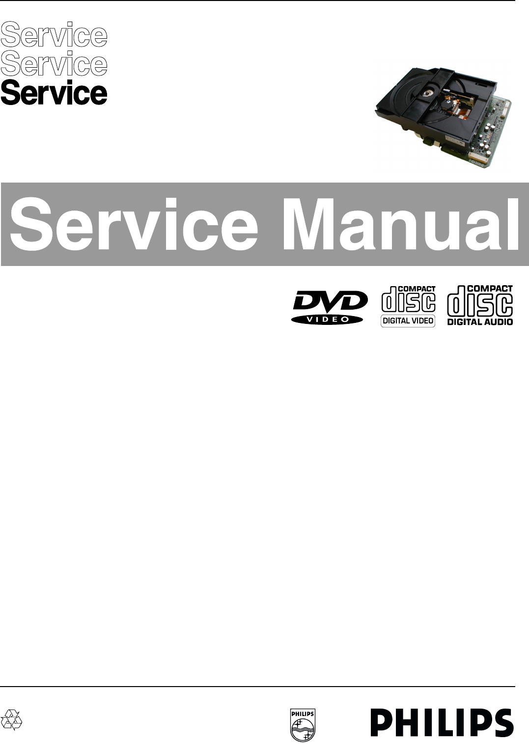
Published by MT0065 Service DPS Hasselt Printed in the Netherlands Subject to modification 53122 785 10840
©
Copyright reserved 2000 Philips Consumer Electronics B.V. Eindhoven, The
Netherlands. All rights reserved. No part of this publication may be reproduced,
stored in a retrieval system or transmitted, in any form or by any means, electronic,
mechanical, photocopying, or otherwise without the prior permission of Philips.
DVD-Video Player DVD Module ASD-1
(Euro) 3104 129 21910
(Non euro) 3104 129 21920
CL06532065-000.eps
180500
Contents Page
1 Technical specifications 2
2 Warnings and remarks 4
3 Directions for use (not available) 6
4 Mechanical instructions 7
5 Test instructions 9
Diagnostic software description 17
6 Block diagram Servo part 29
Block diagram Digital part 30
7Electrical diagrams & pwb’s Diagr. PWB
Servo DALAS (Diagram 1) 31 37-42
Servo MACE (Diagram 2) 32 37-42
Decoder (Diagram 3) 33 37-42
Memory (Diagram 4) 34 37-42
STI 5505 (Diagram 5) 35 37-42
Service interface and back-end (Diagram 6) 36 37-42
Testpoint overview 43 37-42
8 Alignments (not available) 45
9 IC Descriptions 45
10 Sparepart list 85

Technical Specifications
GB 2 ASD-11.
1. Technical Specifications
1.1 Connections
1.1.1 Connector 1600: Supply input connector.
1. +3V3stby
2. +3V3stby
3. +5V
4. +5Vstby
5. Vreserved
6. GND
7. GND
8. GND
9. -8Vstby
10. Standby control line
11. +12Vstby
12. GND
1.1.2 Connector 1603: A/V 1 connector.
1. P50
2. Blue Video
3. Green Video
4. GND
5. Red Video
6. CVBS
7. GND
8. Slow blanking scart
9. -8Vstby
10. +5V
11. +5V
12. Audio mute
13. GND
14. I2S data0 out
15. I2S wordselect
16. I2S bitclock
17. GND
18. I2S systemclock
19. Center_on
20. Kar_bypass
21. Kar_bypass
22. GND
1.1.3 Connector 1604: A/V 2 connector.
1. GND
2. Hor. sync.
3. GND
4. I2S data 2 out
5. GND
6. I2S data 1 out
7. -8Vstby
8. I2C clock
9. +12Vstby
10. I2C data
11. Vreserved
12. +3V3
13. GND
14. C video
15. GND
16. Y video
1.1.4 Connector 1501: I2C interface connector.
1. I2C clock
2. GND
3. I2C data
4. Standby control line
5. P50
1.1.5 Connector 1602: Service connector.
1. TXD
2. Service activation
3. RXD
4. Reserved for RTS
5. 5: GND
6. Reserved for CTS
7. +5V
1.2 Signal specifications
This the specification of all signals as described under
“Connections”
H = +5V ±0.5V
h = 3V3 ±0.3V
L = 0V ±0.5V
l = 0V ±0.3V
Stby : If the set supports a
“standby” function, all
supply voltages
marked with “stby”
have to stay on during
standby.
Standby control line : HStandby mode
: LOn mode.
P50 : Connection between
front and A/V board,
and can be used as
P50 signal line. The
signal is not
connected to the
module electronics.
Slow blanking scart : This signal switches
between
: 0V (220Ωoutput
impedance)
: 12Vstby/2 (455Ω
output impedance)
: 12vstby (690Ω output
impedance)
Audio mute : Can be used for audio
mute transistors
during stop or power
on/off.
: Mute on : +5Vstby
: Mute off: -8Vstby via a
10kΩ resistor.
I2S data0 out : I2S front data output.
: Level h/l
I2S wordselect / I2S bitclock : I2S timing signals
: Level h/l
I2S systemclock : 256xFS audio
systemclock.
: Level H/L
Kar_bypass : Bypasses the karaoke
chip on the A/V board.
: Bypass activeH
: Bypass offL
Center_on : Switches the center
audio to the scart
output.
: Center to scarth
: L/R to scartl
SPDIF out : Digital audio output
: Level H/L

Technical Specifications GB 3ASD-1 1.
Hor. Sync : Video Horizontal
synchronisation
: Level h/l
I2S data1 out : I2S surround data
output.
: Level: h/l.
I2S data2 out : I2S center/sub data
output.
: Level h/l.
I2C clock / I2C data : I2C databus
: Level: H/L
TXD / RXD / RTS / CTS : Service UART to be
connected direct to
PC serial input.
: Output levelsH/L
: Input levelsRS232
compliant
Service activation : Signal openNormal
module start-up
: Signal tied to GND
Module start-up in
service mode.
Vreserved : Reserved in case the
A/V board requires an
extra supply voltage.
: This supply is limited
by a positive polarised
47uF/16V elco +
100nF/16V.
1.3 Performance:
1.3.1 Digital output
CDDA/LPCM : according IEC958
MPEG1 is converted to LPCM :
MPEG2, AC3 audio. : according IEC1937
DTS. : according IEC61937
amendment 1.
: Digital output level is
0V / 5V with GND as
reference. To meet
the standards a
decouple circuit is
necesary.
1.3.2 I2S output
Accuracy : Up to 24bit.
Sample rate : 44.1kHz / 48kHz.
Standard : Philips I2S output
Number of I2S outputs : 3 (6 channel: Front /
Surround / Center-
Bass)
Deemphasis : Already processed in
module.
Audio source streams : CDDA / MPEG1 /
LPCM / MPEG2 / AC3
: No DTS decoding.
Audio trick modes : Dolby Pro Logic
(multichannel
downmix on front
output)
: 3D sound.
1.3.3 Analog output
The module has no analog audio
ouput. : The analog audio
specification will be
determined by the
external DAC circuit.
1.3.4 Video.
Standards : The video output
standard will follow
the source material.
: The OSD standard is
switchable between
PAL or NTSC.
Outputs : The module has 6
analog outputs (3
f o r m a t s ) : Y / C C V B S
RGB.
Specification. : The output is fully
according PQR3 IMS
except
: Output load>1kΩ to
GND / Cap. load
<47pF.
: Level0.5Vpp with
100% white
: DC-levelSync bottom
= -0.65V ±10%
: Some specification
points are significantly
better then PQR3
: SNR on all video
outputs is better then
60dB.
: Video bandwidth
>5MHz (±3dB)
Warnings and Laser safety instructions
GB 4 ASD-12.
2. Warnings and Laser safety instructions
SHOCK, FIRE HAZARD SERVICE TEST:
CAUTION: After servicing this appliance and prior to returning to customer, measure the resistance between
either primary AC cord connector pins (with unit NOT connected to AC mains and its Power switch ON), and the
face or Front Panel of product and controls and chassis bottom,
Any resistance measurement less than 1 Megohms should cause unit to be repaired or corrected before AC
power is applied, and verified before return to user/customer.
Ref.UL Standard NO.1492.
NOTE ON SAFETY:
Symbol : Fire or electrical shock hazard. Only original parts should be used to replace any part with symbol
Any other component substitution(other than original type), may increase risk or fire or electrical shock hazard.
FATTENTION
Tous les IC et beaucoup d’autres semi-
conducteurs sont sensibles aux décharges
statiques (ESD).
Leur longévité pourrait être considérablement
écourtée par le fait qu’aucune précaution
n’est prise a leur manipulation.
Lors de réparations, s’assurer de bien être
relié au même potentiel que la masse de
l’appareil et enfiler le bracelet serti d’une
résistance de sécurité.
Veiller a ce que les composants ainsi que les
outils que l’on utilise soient également a ce
potentiel.
DWARNUNG
Alle IC und viele andere Halbleiter sind
empfindlich gegen elektrostatische
Entladungen (ESD).
Unsorgfältige Behandlung bei der Reparatur
kann die Lebensdauer drastisch vermindern.
Sorgen sie dafür, das Sie im Reparaturfall
über ein Pulsarmband mit Widerstand mit
dem Massepotential des Gerätes verbunden
sind.
Halten Sie Bauteile und Hilfsmittel ebenfalls
auf diesem Potential.
WAARSCHUWING
Alle IC’s en vele andere halfgeleiders zijn
gevoelig voor elektrostatische ontladingen
(ESD).
Onzorgvuldig behandelen tijdens reparatie
kan de levensduur drastisch doen
verminderen.
Zorg ervoor dat u tijdens reparatie via een
polsband met weerstand verbonden bent met
hetzelfde potentiaal als de massa van het
apparaat.
Houd componenten en hulpmiddelen ook op
ditzelfde potentiaal.
AVVERTIMENTO
Tutti IC e parecchi semi-conduttori sono
sensibili alle scariche statiche (ESD).
La loro longevita potrebbe essere fortemente
ridatta in caso di non osservazione della piu
grande cauzione alla loro manipolazione.
Durante le riparazioni occorre quindi essere
collegato allo stesso potenziale che quello
della massa dell’apparecchio tramite un
braccialetto a resistenza.
Assicurarsi che i componenti e anche gli
utensili con quali si lavora siano anche a
questo potenziale.
All ICs and many other semi-conductors are
susceptible to electrostatic discharges (ESD).
Careless handling during repair can reduce
life drastically.
When repairing, make sure that you are
connected with the same potential as the
mass of the set via a wrist wrap with
resistance.
Keep components and tools also at this
potential.
WARNING
Safety regulations require that the set be restored to its original condition
and that parts which are identical with those specified be used.
Veiligheidsbepalingen vereisen, dat het apparaat in zijn oorspronkelijke
toestand wordt terug gebracht en dat onderdelen, identiek aan de
gespecifieerde worden toegepast.
Bei jeder Reparatur sind die geltenden Sicherheitsvorschriften zu beachten.
Der Originalzustand des Gerats darf nicht verandert werden.
Fur Reparaturen sind Original-Ersatzteile zu verwenden.
Le norme di sicurezza esigono che l’apparecchio venga rimesso nelle
condizioni originali e che siano utilizzati pezzi di ricambiago idetici a quelli
specificati.
Les normes de sécurité exigent que l’appareil soit remis a l’état d’origine et
que soient utilisées les pièces de rechange identiques à celles spécifiées.
“Pour votre sécurité, ces documents
doivent être utilisés par des
spécialistes agrées, seuls habilités à
réparer votre appareil en panne.”
GB NL
I
D
I
F
GB
NL
CL 96532065_002.eps
120799
Warnings and Laser safety instructions GB 5ASD-1 2.
LASER SAFETY
This unit employs a laser. Only a qualified service person should remove the cover or attempt to service thi
s
device, due to possible eye injury.
LASER DEVICE UNIT
Type: Semiconductor laser GaAlAs
Wave length: 650 nm (DVD)
780 nm (VCD/CD)
Output Power: 7 mW (DVD)
10 mW (VCD/CD)
Beam divergence: 60 degree
USE OF CONTROLS OR ADJUSTMENTS OR PERFORMANCE OF PROCEDURE OTHER THAN THOS
E
SPECIFIED HEREIN MAY RESULT IN HAZARDOUS RADIATION EXPOSURE.
AVOID DIRECT EXPOSURE TO BEAM
WARNING
The use of optical instruments with this product will increase eye hazard.
Repair handling should take place as much as possible with a disc loaded inside the player
WARNING LOCATION: INSIDE ON LASER COVERSHIELD
CAUTION VISIBLE AND INVISIBLE LASER RADIATION WHEN OPEN AVOID EXPOSURE TO BEAM
ADVARSEL SYNLIG OG USYNLIG LASERSTRÅLING VED ÅBNING UNDGÅ UDSÆTTELSE FOR STRÅLING
ADVARSEL SYNLIG OG USYNLIG LASERSTRÅLING NÅR DEKSEL ÅPNES UNNGÅ EKSPONERING FOR STRÅLEN
VARNING SYNLIG OCH OSYNLIG LASERSTRÅLNING NÄR DENNA DEL ÄR ÖPPNAD BETRAKTA EJ STRÅLEN
VARO! AVATT AESSA OLET ALTTIINA NÄKYVÄLLE JA NÄKYMÄTTÖMÄLLE LASER SÄTEILYLLE. ÄLÄ KATSO SÄTEESEEN
VORSICHT SICHTBARE UND UNSICHTBARE LASERSTRAHLUNG WENN ABDECKUNG GEÖFFNET NICHT DEM STRAHL AUSSETSEN
DANGER VISIBLE AND INVISIBLE LASER RADIATION WHEN OPEN AVOID DIRECT EXPOSURE TO BEAM
ATTENTION RAYO NNEMENT LASER VISIBLE ET INVISIBLE EN CAS D'OUVERTURE EXPOSITION DANGEREUSE AU FAISCEAU
!
CL 06532065_051.eps
230500

Directions for use
GB 6 ASD-13.
3. Directions for use
There is no DFU available
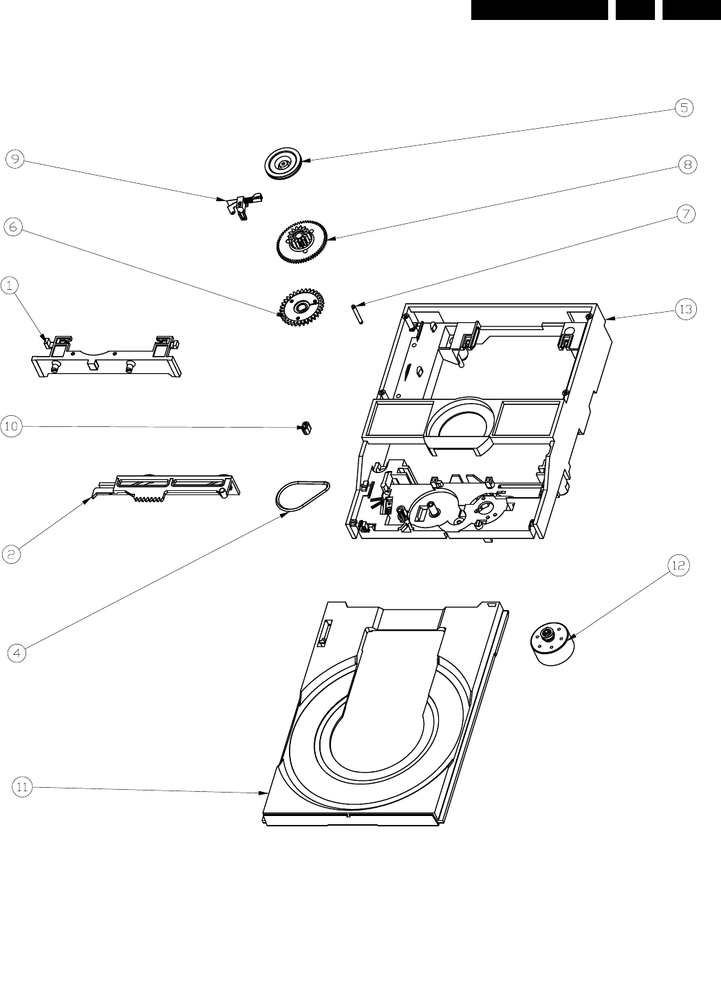
Mechanical instructions GB 7ASD-1 4.
4. Mechanical instructions
4 4822 358 10266 BELT
9 3139 198 80010 SWITCH
10 4822 532 13097 TULE
11 3139194 00270 TRAY
12 3139 197 50060 TRAY MOTOR ASSY CL06532065-001.eps
180500
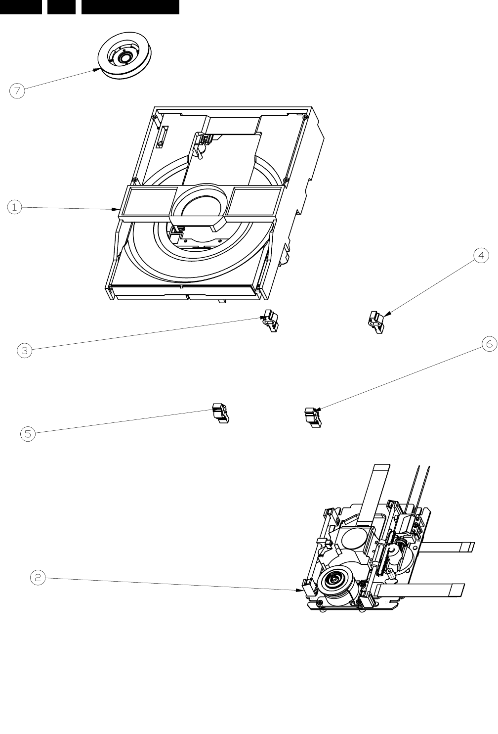
Mechanical instructions
GB 8 ASD-14.
9305 023 61101 VAL6011/01 LOADER COMPLETE
1 3139 197 60090 GENEVA LP LOADER ASSY
2 9305 022 60101 VAM6001/01
3+4 3139 194 00710 SUSPENSION (YELLOW)
5+6 3139 194 00620 SUSPENSION (BLUE)
7 3139 197 60060 CLAMPER ASSY CL06532065-002.eps
180500
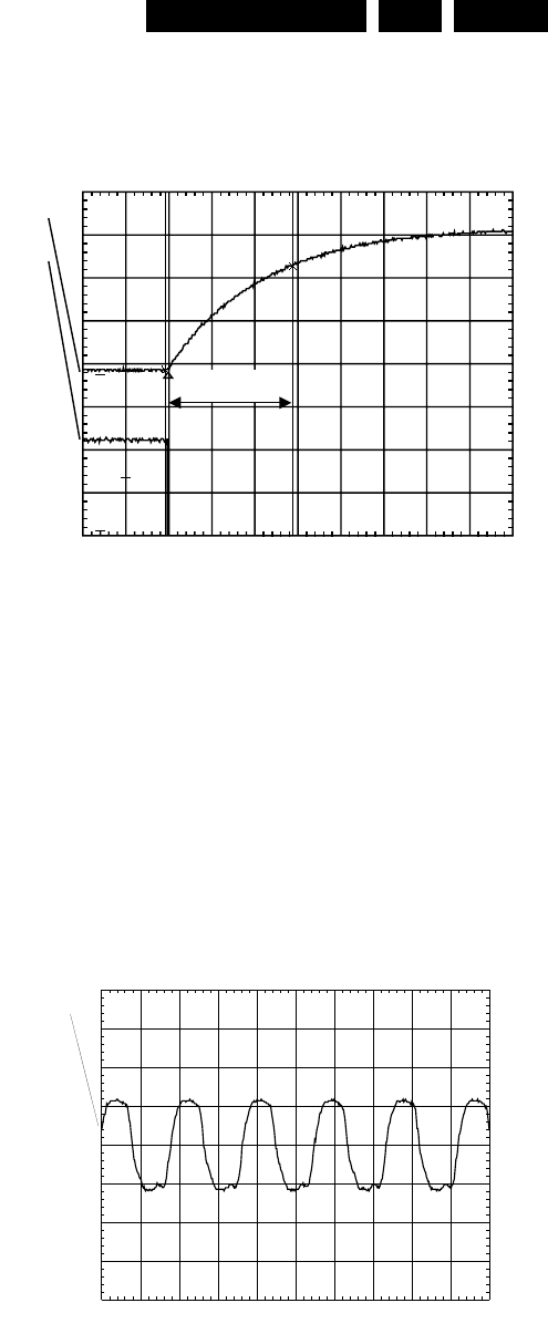
Test instructions mono board DVD-ASD1 GB 9ASD-1 5.
5. Test instructions mono board DVD-ASD1
5.1 General
• Impedance of measuring-equipment should be > 1MΩ.
• Most tests have to be done by software commands.
Together with the software command you will find a Ref.#
nbr. This is the number of the diagnostic nulceus used for
this test. More detailed information can be find in the
chapter “Diagnostic Nuclei”.
• Levels: Most measurements are digital measurements.
The high and low levels in this document got to have next
specification:
low : < 0.3V
high : > 3.0V
LOW : < 0.4V
HIGH : > 4.5V
• All voltages marked with “stby” have to stay on during
standby.
5.2 General start-up measurements
5.2.1 Supply check:
Pin nbr. Supply
1600-1 3V3
1600-2 3V3
1600-3 +5V0V during STAND BY
1600-4 +5Vstby
1600-5 +6V
1600-6 0V
1600-7 0V
1600-8 0V
1600-9 -8V
1600-10 0V5V during STAND BY
1600-11 +12Vstby
0V
Check the supply currents to be sure there are no large failures
on the board. Before measuring the currents, make sure that
no A/V board, display board or Mercury 1 loader is connected
to the mono board and that the PC interface cable is connected
to the board.
Also check if the servo part gets its power.
Testpoint F608: +3V3 ±5%
Testpoint F101: +9V ±5%
The supply currents can be measured using a Tektronix
AM503B current probe.
Supply power consumption
3V3 400mA ±10%
5V 370mA ±10%
5Vstby < 5mA
-8V 55mA ±10% fluctuation: ±20mA
12Vstby 30mA ±20% fluctuation: ±150mA
5.2.2 Reset check:
The reset circuit is triggered by the stand-by line. First make
sure that the STB_CONT line is HIGH by connecting 5V to
testpoint F505.
Then switch STB_CONT over to LOW and check next timing at
the STI5505 reset input (testpoint F503):
Figure 5-1
T 1 = 150msec ±25% (From 0V to 3V3 -3db)
If the reset input doesn’t go high then check the circuit around
transistor 7501.
5.2.3 Clock check
To check the correct functioning of the STI5505, we first have
to check the presence of all clocks.
All clocks to be measured with 0.02% tolerance.
Clock-name Testpoint Frequency
27M_CLK F051 27MHz
PCM_CLK F566 11.2896MHz
Figure 5-2
PM3392A
ch2
ch1 ch1: dT= 148ms dV=2.41 V
CH1 1.00 V=
CH2 0.2 V= MTB50.0ms- 2.10dv ch2-
1
2
T
T1
RESET TIMING CL06532065_003.eps
180500
PM3394B
ch1
CH1 2.00 V~ MTB20.0ns ch1+
1
CL06532065_004.eps
180500
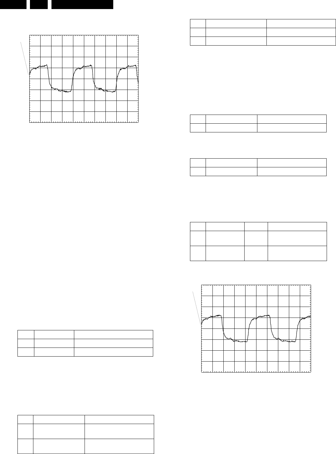
Test instructions mono board DVD-ASD1
GB 10 ASD-15.
Figure 5-3
5.3 µ
µµ
µP environment:
5.3.1 General:
All the tests are carried out by software tests. To start the
software tests, connect a PC to the serial bus of the STI5505.
Use connector 1602 for this connection:
Connector pin Signal
1602-1 TXD (STI5505 out)
1602-2 Service-mode select
1602-3 RXD (STI5505 in)
1602-4 RTS (STI5505 out)
1602-5 GND
1602-6 CTS (STI5505 in)
1602-7 +5V
Now start the terminal program. Make sure that the service-pin
of the µP is pulled low
(pin 1602-2) and then reset the µP (make the STB_CONT line
low). The terminal program of your PC should now display:
“DVD2 Diagnostic software version ...”. This message already
means that the µP is running. The first 5 commands from the
diagnostic software will be carried out automaticly during
diagnostic start-up. The other commands can be carried out by
selecting the “command input”. Just type the reference nbr. to
do the test.
To be sure that the µP is able to run the diagnostic software,
serial port will be checked during start-up.
5.3.2 Memory check:
The µP has a data bus that is connected to a DRAM (not
present!!) and a Flash.
The µP has also an internal link to the MPEG SDRAM
interface.
Next databus checks will be done at start-up to check this data-
bus and SDRAM bus.
There are 2 memory checks left that can be done by hand
command
5.4 General I/O port & peripherals check
5.4.1 I2C bus / EEprom check
To access the EEprom, the I2C bus is used. So by writing and
reading to the EEprom the chip and the bus is checked. With
next commands a certain byte is written to the EEprom. The
original information will always be written back into the
EEprom.
The complete Eeprom can also be checked on failures by
writing to all addresses and reading back. This test takes a long
time (110 sec).
5.4.2 Audio clock switch check
For a DVD disc the audio clock has to be switched from
44.1KHz sampling to 48KHz sampling.
To do so IO-port 1 / 4 has to be switched. Send next commands
and check the audio-clock
Figure 5-4
Ref. # Reference Name Remark
(1) BasicSpAcc Serial port Access test/initialisation
(2) BasicDramWrR DRAM Write Read
Ref. # Command Name Remark
(2b) BasicInterconSDRAM Data and address bus
Interconnection
(2c) BasicInterconFlash Data and address bus
Interconnection
PM3394B
ch1
CH1 2.00 V~ MTB20.0ns ch1+
1
CL06532065_005.eps
180500
Ref. # Command Name Remark
6 PapChksFl Checksum FLASH
16 CompSdramWrR SDRAM Write Read
Ref. # Command Name Remark
11 PapI2cNvram I2C NVRAM access
Ref. # Command Name Remark
15 PapNvramWrR NVRAM Write Read
Ref. # Remark Testpoint Frequency
7a (Clock A_CLK in
44.1kHz mode)
F566 11.2896MHz ± 0.02%
7b (Clock A_CLK in
48kHz mode)
F566 12.288MHz ± 0.02%
PM3394B
ch1
CH1 2.00 V~ MTB20.0ns ch1+
1
CL06532065_006.eps
180500
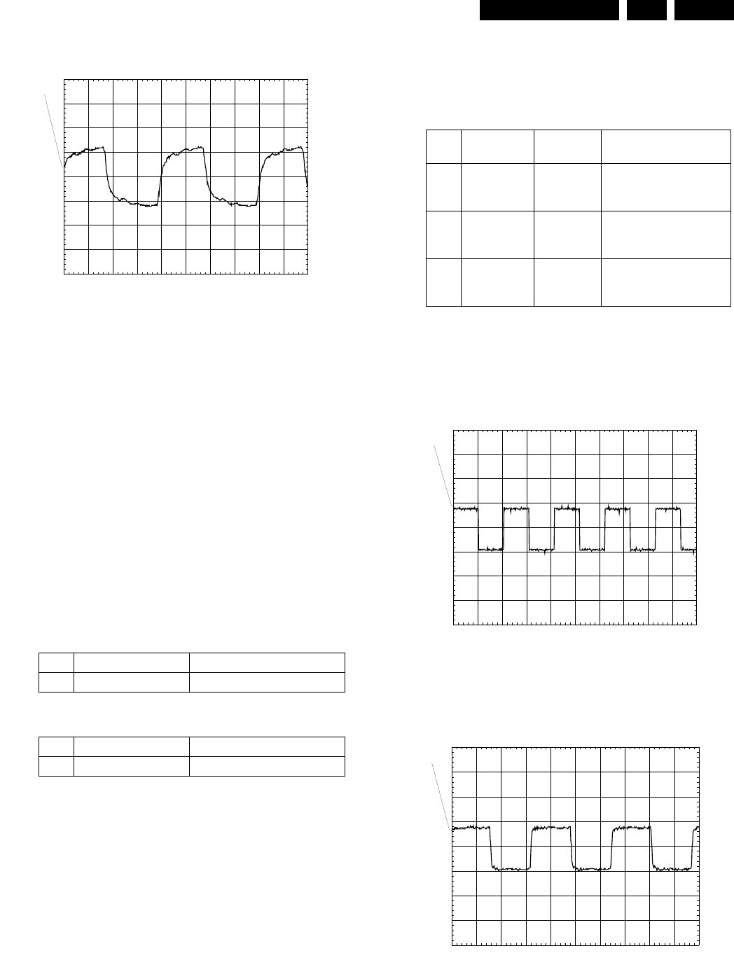
Test instructions mono board DVD-ASD1 GB 11ASD-1 5.
Figure 5-5
5.4.3 Audio deemphasise check
The STI5505 output pins PIO 4-0 and PIO 4-1 were used to
switch deemphasis on a previous type of DAC. This function is
not used anymore, because deemphasis is done internally in
STI5505, but the name still remains. The lines are now used for
a series of functions such as centre_on_stereo or
karaoke_bypass. The PIO 4-0 has got a pull-up to +5V and the
PIO 4-1 has not. To check these pins these commands can be
used.
Ref. # Command Name Remark Testpoint Value
18e AudioDeemp0TristateOn PIO 4-0 Tristate On------
56a AudioDeemp0On PIO 4-0 OnF630 HIGH
56b AudioDeemp0Off PIO 4-0 0 OffF630 low
18f AudioDeemp0TristateOff PIO 4-0 Tristate Off------
56c AudioDeemp1On PIO 4-1 OnF633 high
56d AudioDeemp1Off PIO 4-1 OffF633 low
5.4.4 Audio mute check
Switch on the Mute circuit by sending next command:
Check the Mute output again at testpoint F625: 4.7V ±10%
Switch off the Mute circuit by sending next command
Check the Mute output at testpoint F625: -8V ±10%
5.4.5 Audio I2S check
To check the audio output, connect a audio DAC to the I2S
output (DVD950 A/V board) and start-up the audio test. Look at
the audio outputs from the A/V board for both sine and pink
noise.
The audio signal (sine or pink noise) will also be present on the
digital ouput (SPDif). This can be checked by connecting an
amplifier with digital input.
Check the I2S output.
LRCLK at testpoint F641
Figure 5-6
SCLK at testpoint F637
Figure 5-7
PCM_OUT0 at testpoint F638
PCM_OUT1 at testpoint F659
PCM_OUT2 at testpoint F658
Ref. # Command Name Remark
19a AudioMuteOn AudioMuteOn
Ref. # Command Name Remark
19a AudioMuteOff AudioMuteOff
PM3394B
ch1
CH1 2.00 V~ MTB20.0ns ch1+
1
CL06532065_007.eps
180500
Ref. # Command
Name
Remark Audio outputs
21a AudioSineOn Audio Sine
signal Off
Audio Sine signal On
Sine, 1kHz on stereo
Press stop button
20a AudioPinkNoi
seOn
Audio
Pinknoise
On
Pink Noise on 6 channels
20b AudioPinkNoi
seOff
Audio
Pinknoise
Off
PM3394B
ch1
CH1 2.00 V~ MTB10.0us ch1+
1
CL06532065_008.eps
180500
PM3394B
ch1
CH1 2.00 V~ MTB 100ns ch1+
1
CL06532065_009.eps
180500
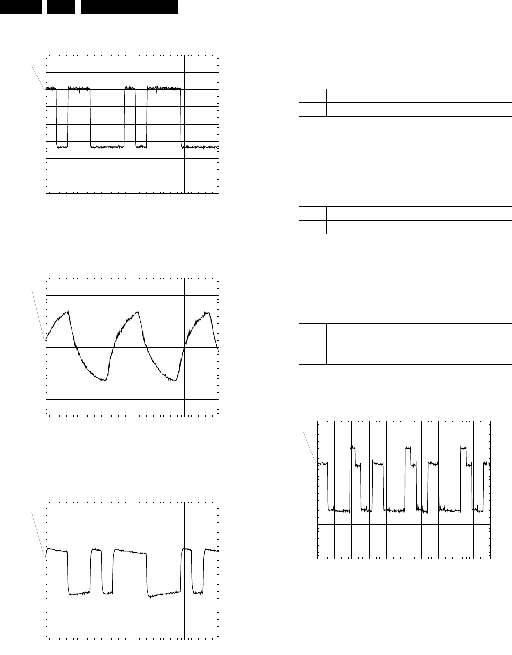
Test instructions mono board DVD-ASD1
GB 12 ASD-15.
Figure 5-8
PCM_CLK at testpoint F640
Figure 5-9
SPDIF at testpoint F644
Figure 5-10
To switch the audio signal off, press the STOP button on the
front.
Without A/V board all levels should be switching between low
and high except:
– PCM_OUT1 and PCM_OUT2 only between low and high
for pink noise. For sine, this is low.
– PCM_CLK and SPDIF switches between LOW and HIGH
Alternatively, there is a check that can be done without A/V
board.
First, let the decoder generate pink noise on the audio outputs.
Measure then these signals on level and frequency.
Signal Level between Frequency
LRCLK low/high 48kHz ± 0.02%
SCLK low/high 3.072MHz ± 0.02%
PCM_CLK LOW/HIGH 12.288 MHz ± 0.02%
PCM_OUT0, 1, 2 low/high N/A
SPDIF LOW/HIGH N/A
Put the pink noise off:
5.5 VIDEO
5.5.1 Video output check
Check DC output-level at all video-outputs at conn 1603-
2,3,5,6 and conn 1604-16: -0.65V ± 10%
Generate a color-bar via next software commands:
Check video output at the next testpoints:
F646: R_VID
Figure 5-11
F649: G_VID
PM3394B
ch1
CH1 1.00 V~ MTB 500ns ch1+
1
CL06532065_010.eps
180500
PM3394B
ch1
CH1 1.00 V~ MTB20.0ns ch1+
1
CL06532065_011.eps
180500
PM3394B
ch1
CH1 2.00 V~ MTB 250ns ch1+
1
CL06532065_012.eps
180500
Ref. # Command Name Remark
20a AudioPinkNoiseOn Audio Pinknoise On
Ref. # Command Name Remark
20b AudioPinkNoiseOff Audio Pinknoise Off
Ref. # Command Name Remark
23a VideoColDencOn Colourbar DENC On
23b VideoColDencOff Colourbar DENC Off
PM3394B
ch1
CH1 200mV~ MTB20.0us ch1+
1
CL06532065_013.eps
180500
Test instructions mono board DVD-ASD1 GB 13ASD-1 5.
Figure 5-12
F653: B_VID
Figure 5-13
F657: CVBS
Figure 5-14
F665: C_VID
Figure 5-15
F666: Y_VID
Figure 5-16
5.5.2 Scart-switching voltage
An aditional part of the video-path is the scart-switching
voltage.
This voltage can be 0V, 6V, 12V.
Check at testpoint F620 the output-voltage while using next
commands:
5.5.3 Video Hsync check.
To measure the correctness of this output, F656 should be
checked.
PM3394B
ch1
CH1 200mV~ MTB20.0us ch1+
1
CL06532065_014.eps
180500
PM3394B
ch1
CH1 200mV~ MTB20.0us ch1+
1
CL06532065_015.eps
180500
PM3394B
ch1
CH1 200mV~ MTB20.0us ch1+
1
CL06532065_0163.eps
180500
Ref. # Command Name Remark
25a VideoScartLo Sends out 0V ± 0.5V
25b VideoScartMi Sends out 6V ± 10%
25c VideoScartHi Sends out 12V ± 10%
Ref. # Command
Name
Remark Value
23a VideoColDe
ncOn
Colourbar DENC on15.625 kHz ±
0.02% Vpeak-peak > 3V
23b VideoColDe
ncOff
Colourbar DENC off No
measurements needed
PM3394B
ch1
CH1 200mV~ MTB20.0us ch1+
1
CL06532065_017.eps
180500
PM3394B
ch1
CH1 200mV~ MTB20.0us ch1+
1
CL06532065_018.eps
180500
Test instructions mono board DVD-ASD1
GB 14 ASD-15.
Figure 5-17
5.6 Servo
5.6.1 General start-up measurements:
Reset the Basic Engine part
Check Vref
Name Testpoint Value
Vref F188 2.5V+/-0.3
Check I2S interface
Name Testpoint Value
B_BCLK F347 6.0MHz +/-0.1
Figure 5-18
CL1F33712.0MHz +/-0.2
Figure 5-19
B_WCLKF343HIGH
StopclkF338HIGH
B_SyncF344HIGH
B_V4F348HIGH
5.6.2 Spindle Motor:
Before switching on the discmotor, check the following
testpoints:
Name Testpoint Value
Stby F357 high
Stby-out F355 LOW
Moto1 F361 3V±0.3
Switch the Discmotor on/off with next commands:
Check the following signals when discmotor has been switched
on::
Name Pin nr. Frequency
Stby F357 low
Stby-out F355 HIGH
Moto1 F361 3V±0.5V
A3 F350 see oscillogram
A2 F352 see oscillogram
A1 F353 see oscillogram
Figure 5-20
Ref. # Command Name Remark
44 BeReset Basic Engin
PM3394B
ch1
CH1 2.00 V~ MTB20.0us ch1+
1
HSYNC CL06532065_019.eps
180500
PM3394B
ch1
CH1 2.00 V~ MTB50.0ns ch1+
1
CL06532065_020.eps
180500
Ref. # Command Name Remark
39a BeDiscmotorOn Discmotor on
39b BeDiscmotorOff Discmotor off
PM3394B
ch1
CH1 2.00 V~ MTB50.0ns ch1+
1
CL06532065_021.eps
180500
PM3394B
ch1
CH1 5.00 V~ MTB20.0ms ch1+
1
CL06532065_022.eps
180500
Test instructions mono board DVD-ASD1 GB 15ASD-1 5.
T1 F280 see oscillogram
T2 F368 see oscillogram
T3 F371 see oscillogram
Figure 5-21
VH F365 3V±0.5V
H1+ F354 see oscillogram
H1- F359 see oscillogram
H2+ F364 see oscillogram
H2- F366 see oscillogram
H3+ F367 see oscillogram
H3- F370 see oscillogram
Figure 5-22
Switch the discmotor off.
5.6.3 Radial
Swith the radial control on/off with the following commands:
Check the following signals:
Name Testpoint Value
Rad - F128 4.3V±0.5V
Rad + F121 4.3V±0.5V
Figure 5-23
Figure 5-24
Check for pulse density signal RA at testpoint F227
Figure 5-25
Check if laser is switched on (visual check of laserlight).
Switch the radial control off.
Ref. # Command Name Remark
40a BeRadialOn Radial control on
40b BeRadialOff Radial control off
PM3394B
ch1
CH1 2.00 V~ MTB2.00ms ch1+
1
CL06532065_023.eps
180500
PM3394B
ch1
CH1 200mV~ MTB2.00ms ch1+
1
CL06532065_024.eps
180500
PM3394B
ch1
CH1 200mV~ MTB 100us ch1+
1
CL06532065_025.eps
180500
Test instructions mono board DVD-ASD1
GB 16 ASD-15.
5.6.4 Sledge
Use the following commands to move the sledge:
Check pulse density signal SL at testpoint F221
Figure 5-26
Name Testpoint Value
Sl - F012 4.5V±0.5V
Sl + F011 4.5V±0.5V
Measure peak to peak signal on SL- and SL+ while moving
sledge outwards.
Name Testpoint Value
Sl - F012 10Vptp +/-0.5
Sl + F011 10Vptp +/-0.5
Measure input sledge control (sledge in home position)
Name Testpoint Value
Sinph F182 2.2V±0.5V
Cosph F192 2.2V±0.5V
5.6.5 Tray:
To open and close the tray use the following commands:
Measure the driver outputs of the BA5938FM for the tray
closed.
Name Testpoint Value
Vo2 - F116 4.3V±2.0V
Vo2 + F111 4.3V±2.0V
Measure again the driver outputs while the tray is opening.
Name Testpoint Value
Vo2 - F116 2.0V±1.0V
Vo2 + F111 6.0V±1.0V
5.6.6 Focus
To switch the Focus motor on/off, use the following commands:
Measure the driver outputs of the BA5938FM for the Focus off.
Name Testpoint Value
foc - F124 4.3V±0.5V
foc + F127 4.3V±0.5V
Switch the focus on
Measure again the driver outputs
Name Testpoint Value
Foc - (sawtooth) F124 1V±0.2V
Foc + (sawtooth) F127 1V±0.2V
Figure 5-27
Check for pulse density signal FO at testpoint F234
Figure 5-28
Check for laserlight.
Switch the focus off
5.6.7 Hf path
Play DVD test disc.
Measure outputs of diodes A, B, C, D, E, F.
Name Testpoint Value
A F140 2.6V±0.2V
B F141 2.6V±0.2V
C F143 2.6V±0.2V
D F144 2.6V±0.2V
E F147 2.6V±0.2V
F F148 2.6V±0.2V
At outputs of diodes A, B, C, D the following oscillogram can be
measured:
Ref. # Command Name Remark
41a BeSledgeIn Sledge inwards
41b BeSledgeOut Sledge outwards
Ref. # Command Name Remark
43a BeTrayIn Tray in
43b BeTrayOut Tray out
Ref. # Command Name Remark
38a BeFocusOn Focus on
38b BefocusOff Focus off
PM3394B
ch1
CH1 2.00 V~ MTB 500ns ch1+
1
CL06532065_028
180500
PM3394B
ch1
CH1 500mV~ MTB 100us ch1+
1
CL06532065_029.eps
180500
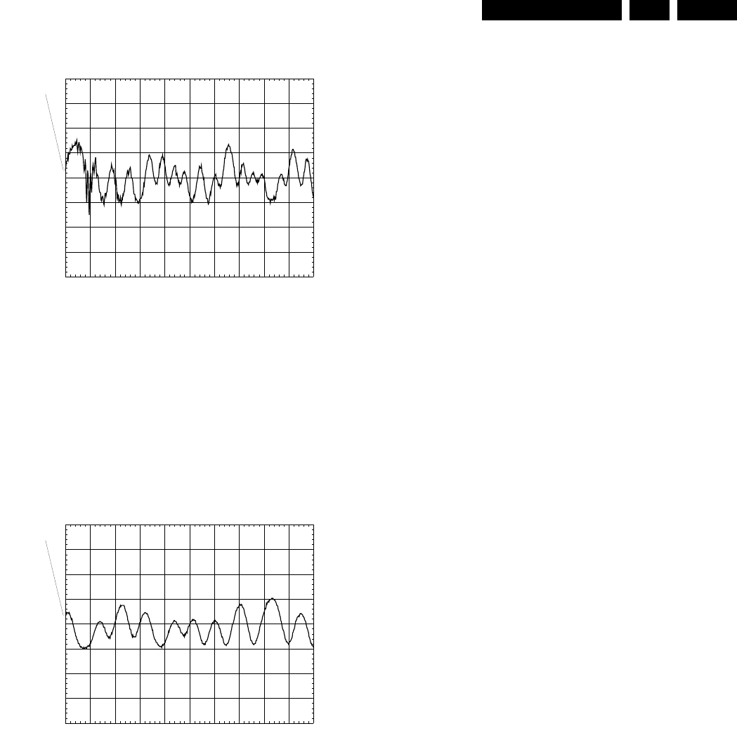
Test instructions mono board DVD-ASD1 GB 17ASD-1 5.
Figure 5-29 cl06532065-031
Measure DVDALAS outputs
Name Testpoint Value
RFO DC F146 2.5V ±0.2V
O1 F156 25mV±10mV
O2 F159 25mV±10mV
O3 F169 25mV±10mV
O4 F166 25mV±10mV
S1 F174 25mV±10mV
S2 F175 25mV±10Mv
At output RFO, the following oscillogram can be measured:
Figure 5-30
5.7 Diagnostic software description
Introduction
5.7.1 Introduction
Purpose
This document describes all interfaces from the outside world
to the diagnostic software, what is needed to use these
interfaces and how to access them.
Changes for DVDv2b are marked.
Scope
This document has been realised within the framework of the
product development of the second generation DVD video
player. This player forms the basis for future DVD
developments as described in the DVDv2 Overall Project
Management Plan.
5.7.2 Definitions and abbreviations
Definitions
Control PC Automatic test equipment, part of the
production control system in the
factory, to control the execution of
Diagnostic Nuclei in the DVD player.
Diagnostic Nucleus Part of the Diagnostic Software. Each
nucleus contains an atomic and
software independent diagnostic test,
testing a functional part of the DVD
player hardware on component level.
Script Part of the Diagnostic Software. Each
script contains a sequence of
Diagnostic Nuclei to be executed.
Service PC PC used by a service- or repair-person
to communicate with the Diagnostic
Software in the DVD player.
Abbreviations
FDS Full Diagnostic Software
5.8 Overview of Interfaces
The table below shows an overview of the user interfaces of the
Diagnostic Software. The table is based on logical interface,
interfaces as seen from user perspective. A logical interface
can use one or more physical interface components. The DVD
has only a single RS232 port, implying that all interfaces using
this port are mutually exclusive.
PM3394B
ch1
CH1 100mV~ MTB 500ns ch1+
1
CL06532065_031.eps
180500
PM3394B
ch1
CH1 500mV~ MTB 250ns ch1+
1
CL06532065_032.eps
180500
Test instructions mono board DVD-ASD1
GB 18 ASD-15.
In the next chapters the logical user interfaces are described in
more detail including the exact use of the physical interface
components.
5.9 Description Of Interfaces
5.9.1 Menu Interface
The menu interface is part of the Level 2 / Second Line
diagnostic mode. Via the menu interface it is possible to control
the execution of the Diagnostic Nuclei.
Set-up physical interface components
Hardware required:
• Service PC
• one free COM port on the Service PC
• special cable to connect DVD player to Service PC
The service PC must have a terminal emulation program (e.g.
OS2 WarpTerminal or Procomm) installed and must have a
free COM port (e.g. COM1). Activate the terminal emulation
program and check that the port settings for the free COM port
are: 19200 bps, 8 data bits, no parity, 1 stop bit and no flow
control. The free COM port must be connected via a special
cable to the RS232 port of the DVD player. This special cable
will also connect the test pin, which is available on the
connector, to ground (i.e. activate test pin).
5.9.2 Code nr. PC interface cable: 3122 785 90017
Activation
Switch the player on and the following text will appear on the
screen of the terminal (program):
The first line indicates that the Diagnostic software has been
activated and contains the version number of the diagnostic;
this is also an indication that the first basic nucleus (nucleus
number 1) has been executed succesfully. The next three lines
are the succesful result of the subsequent basic tests (nuclei 2,
3, 4 and initialisation of Karaoke chip respectively). If not all
these messages appear on the terminal screen, then the
related nucleus found an error. The last line is the prompt
asking to choose for an interface form. If a choice for Menu
Interface has been made, the main menu will appear. For the
layout of the menus, see page 25.
To switch between interfaces, the DVD player needs to be
switched off and on again.
Note1 : The DVDv2B player has no power-ON key, but should
be turned on by connecting the power-cable.
Note2 : The Dram tests are no longer executed because the
player has no DRAM .
Note3 : When the stack is located in the internal memory, the
test with the SRAM doesn't work and will be left out.
Note4 : The karaoke initialisation will also take place if there is
no karaoke-chip in the player.
Usage
A selection can be given by the user by typing the number of
the menu-item chosen at the prompt. Each entry must be
terminated with a . Invalid selections will cause an error
message by the Menu Handler. Example:
Result and output of an activated (and terminated) nucleus will
be sent back to the service terminal. Example:
After the user presses a key, the current menu is rebuilt on
screen.
Pressing < return > at the prompt without any further input at
the terminal will always rebuild the main menu.
Termination
The menu interface is terminated by switching off the DVD
player.
Logical
Interface Description
Physical interface
components
Menu
Interface
Menu-driven
activation of
individual nuclei,
used for Level 2/
Second Line
diagnostic mode.
Users are service or
repair people
Service PC running a
terminal emulation
program, connected to
the RS232 port of the
DVD player Test pin
Command
Line Interface
Used during Level 1
diagnostic mode.
Used to send
commands from the
Control PC into the
DVD hardware.
Control PC, running a
control program (e.g.
Asterix), connected to
RS232 port of the DVD
player Test pin
Script
Interface
Used to execute
Player Test Script
(including reading
the error log) and
Dealer Test Script.
Local keyboard Local
display
S2B interface Used for S2B
communication with
the Basic Engine
Service PC, running a
S2B monitor program,
connected to the
RS232 port of DVD
player Test pin
Download
Interface
Used to download
diagnostic software
into the DVD player
Service PC running a
terminal emulation
program, connected to
the RS232 port of the
DVD player Test pin
CL06532065-033.eps
180500
CL96532111_021.eps
071099
CL96532111_022.eps
071099
Test instructions mono board DVD-ASD1 GB 19ASD-1 5.
5.9.3 Command Line Interface
The command line interface is part of level 1 diagnostic mode.
Via a command line interface the execution of Diagnostic
Nuclei can be controlled.
Set-up physical interface components
Hardware required:
• Control PC
• one free COM port on the Control PC
• special cable to connect DVD player to the Control PC
The control PC must use the following port settings for the used
COM port: 19200 bps, 8 data bits, no parity, 1 stop bit and no
flow control. The control PC is connected with a special cable
to the RS232 port of the DVD player. Via the same connection
the test pin will be connected to ground.
Activation
After power on the next text will sent to the control PC
The first line indicates that the Diagnostic software has been
activated and contains the version number; this is also an
indication that the first basic nucleus (nucleus number 1) has
been executed succesfully. The next three lines are the
succesful result of two subsequent basic tests (nuclei 2, 3,
4and karaoke initialisation respectively). If not all these
messages appear on the terminal screen, then the related
nucleus found an error. The fifth line lets the user choose
between the two possible interface forms. The last line is the
prompt ("DD>"). The diagnostic software is now ready to
receive commands.
Note1 : The DVDv2B player has no power-ON key, but should
be turned on by connecting the power-cable.
Note2 : When it is a player without DRAM, the DRAM tests are
left out.
Usage
The commands that can be given are the names or the
numbers of the nuclei. A command must be terminated with a
< return > character from the control PC. When typing
commands, the backspace key can be used to make
corrections.
In case of typing errors in the command, an error message is
returned. Example:
If the command (the nucleus name or number) is recognised,
the nucleus is executed. Result and output of an activated (and
terminated) nucleus will be sent back to the control PC
according to the standard layout as defined in Appendix C.
Example in case the command is correct:
Example in case the result is an error:
Termination
The command line interface is terminated by switching off the
DVD player.
5.9.4 S2B Interface (not for service)
Set-up physical interface components
Hardware needed:
• Control PC
• one free COM port on the Control PC
• special cable to connect DVD player to Control PC
• S2B monitor tool running on the Control PC
Activation
To start the S2B interface, connect the RS232 cable to the
Control PC in the correct manner. Then start the PC, start the
monitor tool and start the DVD player; turn off the monitor tool,
turn on S2B monitor tool. The S2B monitor tool now takes all
communication.
The S2B interface is activated by sending the bit pattern 110x
xxxx with the first character to the DVD player, when the user
is asked to choose an interface type. The command handler
will then activate the S2B pass-through nucleus. The character
sent will be passed to this nucleus without loss.
Note: The DVDv2B player has no power-ON key, but should be
turned on by connecting the power-cable.
Termination
To terminate S2B pass-through mode, switch off the DVD
player.
5.10 Script Interfaces
This interface is used during execution of the Player Script and
the Dealer Script to display output and error messages.
The local display will be used to display the output and the error
messages.
5.10.1 Dealer Script
Set-up physical interface components
Hardware required:
• DVD player
The DVD player is tested stand-alone: no other equipment than
the DVD player is needed.
Activation
The dealer script is activated by pressing OPEN/CLOSE and
PAUSE on the local keyboard of the DVD player
simultaneously during power-on.
CL06532065_034.eps
180500
CL96532111_024.eps
071099
CL96532111_025.eps
071099
CL96532111_026.eps
071099
Test instructions mono board DVD-ASD1
GB 20 ASD-15.
Note : The DVDv2B player has no power-ON key, but should
be turned on by connecting the power-cable.
Usage
The test requires no user interaction. A number of nuclei will be
run before a message is returned indicating if there is a failure
in the DVD player.
During the execution of a script, a progress indicator is
displayed on the local display of the DVD player.
The counter at the right side of the display counts down from
the number of nuclei to be run to zero. At zero all nuclei from
the script have been run and the result (PASS/Error) is
displayed on the local display of the DVD player.
When the dealer script has been completed, the results are
displayed in the following manner:
Termination
To turn off the dealer test, the DVD player must be powered
down.
5.10.2 Player Script
Set-up physical interface components
Hardware needed:
• DVD player
• television set, connected to the DVD player
• 6 audio speakers
• an external video source
Activation
To activate the player script, press OPEN, CLOSE and STOP
keys on the local keyboard of the DVD player simultaneously
during power-on.
Usage
The player test requires human interaction to decide whether
nuclei give correct output, e.g. the user needs to confirm the
results of the display test. This needs to be given through the
local keyboard on the DVD player. Which keys can be used for
this purpose is described with each test.
Module test (with user interaction)
During the first phase of the dealer test, the three main modules
(Digital PWB, Display PWB and Basic Engine) are tested;
some interaction from the user is required.
1. Testing the Display PWB
This involves testing the local display and keyboard, but also
testing the remote control and the leds.
The Display Test
During the display test, different patterns will be shown on the
local display of the DVD player. The user needs to step through
these patterns using the PLAY key on the local keyboard. If any
of the displayed patterns is incorrect, the display test has failed,
and also the player test has failed.
The test patterns on display will be repeated in a loop (stepped
through using PLAY) until the user presses NEXT on the local
keyboard to proceed to the next test.
The LED Test
Next is the LED test; the LEDs on the DVD player are lit.
Pressing PLAY will indicate that all LEDs are operational. To
indicate that a LED did not light up, the user must press the
PAUSE key. Pressing PLAY or PAUSE will proceed the user
into the next test.
The Keyboard Test
During the keyboard test, the user needs to press all the keys
on the local keyboard one by one. On the local display each key
is represented by its scancode (a hexadecimal 2-digit code
identifying the key to the DVD player).
Pressing a key will show its representing code on the local
display of the DVD player: the first hexadecimal digit identifies
the key pressed, the second indicates how many times this
particular key was detected. In case the key is pressed more
than once, the scancode is displayed as many times, with the
second digit of its code increased each time. The display of
scancodes scrolls from right to left, with the most recent
scancode at the right. The following example gives a possible
layout of the local display during the display/remote control
test:
To terminate the keyboard test, press the NEXT key on the
local keyboard of the DVD player and keep it pressed for 1
(one) full second. The keyboard test will terminate with a
message on the local display. In case the keyboard test was
successful, the message is:
In case the keyboard test was not successful, the message will
be:
CL96532111_017.eps
071099
CL96532111_018.eps
071099
CL96532111_019.eps
071099
1 ⋅ 2 ⋅ 3 ⋅ 4 ⋅ 5 ⋅ 6 ⋅ 7 ⋅ 8 ⋅ 9 ⋅ 10 ⋅ 11 ⋅ 12 ⋅ 13 ⋅ 14 ⋅ 15 +
CL 96532097_004.eps
130999
1 ⋅ 2 ⋅ 3 ⋅ 4 ⋅ 5 ⋅ 6 ⋅ 7 ⋅ 8 ⋅ 9 ⋅ 10 ⋅ 11 ⋅ 12 ⋅ 13 ⋅ 14 ⋅ 15 +
CL 96532097_007.eps
130999
Test instructions mono board DVD-ASD1 GB 21ASD-1 5.
If the "tbFAIL"-message is displayed, the player test has failed.
This is the end of the player test: turn off the DVD player, or
press NEXT on the local keyboard of the DVD player to
proceed to the next test.
The remote control test
For the remote control test, the user must press a key (any key)
on the DVD's remote control. The display at the start of the test
looks as follows:
When a remote control code has been received, its scancode
is displayed as follows:
The NEXT key can be pressed to exit this test.
However, if the user requires to test all keys on the remote
control, (s)he can continue to press keys and these will all be
displayed on the local display. With a code-table at hand this
test can be used to test the full functionality of the DVD's
remote control.
When the user has pressed NEXT on the local keyboard (NOT
on the remote control!), the result of the remote control test is
shown on the local display as follows:
in case of succes;
if the test fails.
Pressing NEXT on the local keyboard again will proceed to the
next test.
2. Testing the Monoboard
The picture tests involve putting a predefined picture on the
connected television set, and asking the user for confirmation.
When the picture has been put on screen, the local display
asks for confirmation by the user as follows:
If the user presses PLAY, he confirms the test; pressing
PAUSE will indicate a fault in the test. At this time, the player
test had failed and the DVD player can be switched off, or the
user can proceed to the next test by pressing NEXT on the local
keyboard of the DVD player.
Pressing the NEXT key on the local keyboard will start the next
picture test (Colour set-up functional test).
When the picture tests are finished, the sound tests are run.
A predefined sound will be generated, and again the user is
asked to confirm this. The local display looks as follows:
Pressing PLAY confirms the test, PAUSE indicates test failure.
If the test is faulty, the player test failed and the DVD player can
be shut off. Subsequent sound tests will be numbered in
ascending order.
Pressing NEXT on the local keyboard of the DVD player will
take the user into the next test.
3. Testing the Basic Engine
Most tests on the basic engine require user interaction.
When the basic engine tests are started, the version of the
basic engine which is present in the DVD player is shown on
the local display, as follows:
1 ⋅ 2 ⋅ 3 ⋅ 4 ⋅ 5 ⋅ 6 ⋅ 7 ⋅ 8 ⋅ 9 ⋅ 10 ⋅ 11 ⋅ 12 ⋅ 13 ⋅ 14 ⋅
CL 96532097_008.eps
130999
1 ⋅ 2 ⋅ 3 ⋅ 4 ⋅ 5 ⋅ 6 ⋅ 7 ⋅ 8 ⋅ 9 ⋅ 10 ⋅ 11 ⋅ 12 ⋅ 13 ⋅ 14 ⋅ 15 +
CL 96532111_032.eps
071099
1 ⋅ 2 ⋅ 3 ⋅ 4 ⋅ 5 ⋅ 6 ⋅ 7 ⋅ 8 ⋅ 9 ⋅ 10 ⋅ 11 ⋅ 12 ⋅ 13 ⋅ 14 ⋅ 15 +
CL 96532097_009.eps
130999
1 ⋅ 2 ⋅ 3 ⋅ 4 ⋅ 5 ⋅ 6 ⋅ 7 ⋅ 8 ⋅ 9 ⋅ 10 ⋅ 11 ⋅ 12 ⋅ 13 ⋅ 14 ⋅ 15 +
CL 96532097_011.eps
130999
1 ⋅ 2 ⋅ 3 ⋅ 4 ⋅ 5 ⋅ 6 ⋅ 7 ⋅ 8 ⋅ 9 ⋅ 10 ⋅ 11 ⋅ 12 ⋅ 13 ⋅ 14 ⋅ 15 +
CL 96532097_012.eps
130999
1 ⋅ 2 ⋅ 3 ⋅ 4 ⋅ 5 ⋅ 6 ⋅ 7 ⋅ 8 ⋅ 9 ⋅ 10 ⋅ 11 ⋅ 12 ⋅ 13 ⋅ 14 ⋅ 15 +
CL 96532097_013.eps
130999
1 ⋅ 2 ⋅ 3 ⋅ 4 ⋅ 5 ⋅ 6 ⋅ 7 ⋅ 8 ⋅ 9 ⋅ 10 ⋅ 11 ⋅ 12 ⋅ 13 ⋅ 14 ⋅ 15 +
CL 96532097_014.eps
130999
1 ⋅ 2 ⋅ 3 ⋅ 4 ⋅ 5 ⋅ 6 ⋅ 7 ⋅ 8 ⋅ 9 ⋅ 10 ⋅ 11 ⋅ 12 ⋅ 13 ⋅ 14 ⋅ 15 +
CL 96532097_015.eps
130999
Test instructions mono board DVD-ASD1
GB 22 ASD-15.
The version number is displayed in decimal representation (the
underscore replacing the dot). When the user presses NEXT
on the local keyboard, the tests on the basic engine are started.
First, the tray operation is tested. The user can move the tray
in and out by pressing the PLAY or PAUSE key on the local
keyboard (both keys have essentially the same function). The
results need to be checked visually by the user, the software
cannot detect any faults. The local display looks as follows:
To indicate this is a test of which the result is to be checked by
the user, the first word on the local display is "do".
Except for testing the tray, this test is also meant to give the
user the opportunity to put a disc into the DVD player for
subsequent basic engine tests. Some of the following tests
need a disc in the DVD player to operate properly. Always put
a disc into the DVD player during this test! At the end of the
basic engine tests there is opportunity to remove it (before the
looptests start). Pressing the NEXT key on the local keyboard
proceeds to the next test.
Second test is the sledge test; the user is asked to move the
sledge by using the keys PLAY and PAUSE on the local
keyboard (both keys have essentially the same function). This
test needs to be checked visually by the user; the software
cannot detect any faults. The local display during this test looks
as follows:
After pressing NEXT on the local keyboard the discmotor is
tested; the local display looks as follows:
The user is required to listen if the disc motor is running; this
must be confirmed by pressing PLAY on the local keyboard.
The PAUSE key is used to indicate the discmotor does not run.
Pressing NEXT on the local keyboard starts the focus test. The
local display looks as follows during this test:
By pressing PLAY the user confirms successful focussing by
the basic engine; pressing PAUSE indicates a fault in the focus
function.
Pressing NEXT on the local keyboard starts the radial function;
the local display looks as follows:
Again, PLAY confirms the result, PAUSE indicates an error.
After pressing NEXT on the local keyboard, the grooves/jump
test is started. As this is also a test that cannot be checked by
the software, the user needs to perform a visual test. The local
display looks as follows:
By pressing PLAY the next grooves/jump position is taken;
pressing PAUSE will go to the previous grooves/jump position.
Switching through the different positions is done in a cyclic
manner.
Press the NEXT key on the local keyboard to proceed to the
last basic engine test: again, the tray is tested. This has been
done at the beginning of the basic engine test already, the
repeat is only meant to enable the user to remove the disc in
the tray before proceeding. The local display will look as
follows:
Press PLAY or PAUSE to operate the tray; remove the disc in
the tray.
The tray will be closed automatically (if needed) before
proceeding to the next tests (by pressing NEXT on the local
keyboard).
Read Error Log
1 ⋅ 2 ⋅ 3 ⋅ 4 ⋅ 5 ⋅ 6 ⋅ 7 ⋅ 8 ⋅ 9 ⋅ 10 ⋅ 11 ⋅ 12 ⋅ 13 ⋅ 14 ⋅ 15 +
CL 96532097_016.eps
130999
1 ⋅ 2 ⋅ 3 ⋅ 4 ⋅ 5 ⋅ 6 ⋅ 7 ⋅ 8 ⋅ 9 ⋅ 10 ⋅ 11 ⋅ 12 ⋅ 13 ⋅ 14 ⋅ 15 +
CL96532097_017.eps
130999
1 ⋅ 2 ⋅ 3 ⋅ 4 ⋅ 5 ⋅ 6 ⋅ 7 ⋅ 8 ⋅ 9 ⋅ 10 ⋅ 11 ⋅ 12 ⋅ 13 ⋅ 14 ⋅ 15 +
CL 96532097_018.eps
130999
1 ⋅ 2 ⋅ 3 ⋅ 4 ⋅ 5 ⋅ 6 ⋅ 7 ⋅ 8 ⋅ 9 ⋅ 10 ⋅ 11 ⋅ 12 ⋅ 13 ⋅ 14 ⋅ 15 +
CL 96532097_019.eps
130999
1 ⋅ 2 ⋅ 3 ⋅ 4 ⋅ 5 ⋅ 6 ⋅ 7 ⋅ 8 ⋅ 9 ⋅ 10 ⋅ 11 ⋅ 12 ⋅ 13 ⋅ 14 ⋅ 15 +
CL 96532097_020.eps
130999
1 ⋅ 2 ⋅ 3 ⋅ 4 ⋅ 5 ⋅ 6 ⋅ 7 ⋅ 8 ⋅ 9 ⋅ 10 ⋅ 11 ⋅ 12 ⋅ 13 ⋅ 14 ⋅ 15 +
CL 96532097_021.eps
130999
1 ⋅ 2 ⋅ 3 ⋅ 4 ⋅ 5 ⋅ 6 ⋅ 7 ⋅ 8 ⋅ 9 ⋅ 10 ⋅ 11 ⋅ 12 ⋅ 13 ⋅ 14 ⋅ 15 +
CL 96532097_016.eps
130999
Test instructions mono board DVD-ASD1 GB 23ASD-1 5.
The contents of the error log will be displayed on the local
display, as follows :
Note: This is an example only; no actual errorcode is intended
The first two characters on the local display ("EL") indicate that
the read-out mode of the error log is activated. After the hyphen
8 hexadecimal digits (one faultcode) are displayed. Below the
row of 7-segment displays the highlighted number indicates the
number of the faultcode being displayed. (Not for DVDv2B) The
highest number indicates the oldest faultcode.
If, in the future, more than 15 faultcodes need to be displayed,
the "+" character can be used to indicate the display of a
faultcode in the range 16 - 30.
To step through the different fault codes, the PLAY (next) and
PAUSE (previous) key on the local keyboard can be used. The
display of faultcodes is cyclic. If the error log does not contain
any fault codes, all displayed error codes will be "000 00000".
To switch off the display of the error log, the NEXT key must be
pressed on the local keyboard.
Read Error Bits
The error bits are used to indicate that an error occurred once
or more times; if that is the case the bit representing the error
is set. To read out this field of error bits, the local display is
used. Only the numbers of the errors where the bit is set will be
displayed on the local display. The layout of the local display is
(globally) as follows2:
The number of the set bits is displayed in a cyclic manner.
Scrolling through the set error bits can be done with the PLAY
key for 'next' and PAUSE key for 'previous'. Pressing the PLAY
key at the last bit number will display the first bit number again,
pressing the PAUSE button at the first bit number will display
the last bit number in the list. The representation of bit numbers
is decimal.
If no error bits are set, the number on the right side of the
display will be "00"
Module Looptest
The module looptest is an infinite loop in which a number of
nuclei are executed over and over again. The nuclei run are the
same as in the dealer test; user interaction is not required.
During this looptest, the display looks as follows3:
The leftmost three digits indicate which of the DVD player's
modules is faulty; the explanation is in the following table:
After the hyphen the (decimal) number indicates the number of
times the looptest was performed.
The right side of the display shows an error code DNER (in
decimal representation), which is built from a nucleus number
(DN) and an error number (ER). This code indicates the last
nucleus that returned an error code. For explanation of this
DNER code, see document [SDD_DN].
Pressing NEXT on the local keyboard of the DVD player will
exit this loop and show the end result of the player test.
End result of the player test is equal to the last display shown
above: it shows which module is faulty and which nucleus
caused the last error, as well as how many loops were
performed.
Termination
To terminate the player test, switch off the DVD player.
5.11 Download Interfaces (not for service)
The download interface enables the user to download another
version of diagnostic software into the RAM of the DVD player.
The downloaded software will overrule the software which is
placed in the DVD player's ROM; running the original
diagnostic software is disabled until the DVD player is switched
off and on again.
For download of diagnostic software, the RS232 port may be
used.
5.11.1 Set-up physical interface components
Hardware required:
•Service PC
•one free COM port on the Service PC
•special cable to connect DVD player to Service PC
The service PC must have a terminal emulation program (e.g.
OS2 WarpTerminal or Procomm in Windows95) installed and
must have a free COM port (e.g. COM1). Activate the terminal
emulation program and check that the port settings for the free
COM port are: 19200 bps, 8 data bits, no parity, 1 stop bit and
no flow control.
The free COM port must be connected via a special cable to the
RS232 port of the DVD player. This special cable will also
connect the test pin, which is available on the connector, to
ground (i.e. activate test pin).
5.11.2 Activation
Switch the DVD player on and the following text will appear on
the screen of the terminal (emulation program):
1 ⋅ 2 ⋅ 3 ⋅ 4 ⋅ 5 ⋅ 6 ⋅ 7 ⋅ 8 ⋅ 9 ⋅ 10 ⋅ 11 ⋅ 12 ⋅ 13 ⋅ 14 ⋅
CL 96532097_022.eps
130999
1 ⋅ 2 ⋅ 3 ⋅ 4 ⋅ 5 ⋅ 6 ⋅ 7 ⋅ 8 ⋅ 9 ⋅ 10 ⋅ 11 ⋅ 12 ⋅ 13 ⋅ 14 ⋅ 15 +
CL 96532097_023.eps
130999
1 ⋅ 2 ⋅ 3 ⋅ 4 ⋅ 5 ⋅ 6 ⋅ 7 ⋅ 8 ⋅ 9 ⋅ 10 ⋅ 11 ⋅ 12 ⋅ 13 ⋅ 14 ⋅ 15 +
CL 96532097_025.eps
130999
Displayed
Value Indication for each module
Loader Mono-
board
Display
PCB
000 ok ok ok
001 ok ok faulty
010 ok faulty ok
011 ok faulty faulty
100 faulty ok ok
101 faulty ok faulty
110 faulty faulty ok
111 faulty faulty faulty
CL 06532065_052.eps
230500
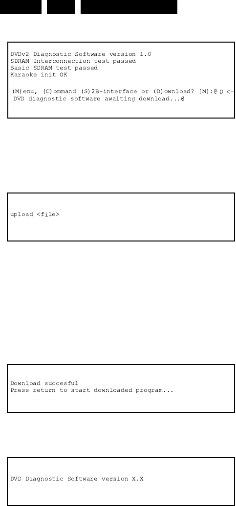
Test instructions mono board DVD-ASD1
GB 24 ASD-15.
The DVD player is now in a wait-mode, awaiting the download
of a file in Motorola S3-format.
Enter the download command (which will be an "upload" from
the terminal!) at the terminal:
Progress seen by the diagnostic software is indicated by
displaying the character "*" on screen repeatedly; if the
download software encounters an error, the end of the
downloaded file will be awaited and instead of the "*"-
character, the "+"- character will be used to indicate
(erroneous) progress.
When download is finished, the following message will come
from the DVD player:
When the user then presses a key, the DVD player will report
and start to run the downloaded software.
Note1 : The DVDv2B player has no power-ON key, but should
be turned on by connecting the power-cable.
Note2 : For players without DRAM, the DRAM-tests will be
scipped.
5.11.3 Usage
The usage of the downloaded software depends on the
contents of that software and cannot be described here.
5.11.4 Termination (not for service)
To exit the download-interface and remove the downloaded
software from the DVD player, switch off the DVD player.
External Scripts
A script is a sequence of nucleus calls. Internal scripts (e.g.
scripts built into the diagnostic software itself) are in the form of
a C-language module. However it cannot be expected from a
customer to write C-modules in order to create new scripts.
The scripts that can be made externally are therefor in one of
the following two forms:
1. A Procomm or Telex script Procomm or Telex can be used
to write diagnostic scripts. The script language of both
communication packages contains possibilities for
construction of loops and branches in the scripts.
Commands then going over the line will be exactly the
same as described in the chapter "Command Interface".
The diagnostic software (the engine) will receive normal
RS232 commands and processes these as defined,
sending results of these nuclei back over the RS232 line.
In the Terminal the Procomm or Telex script determines
which command sequence is followed
2. An Asterix-script Asterix-scripts are C-programs in which
commands are sent to the diagnostic software (the
engine). The construction of branches and loops is again
located in the remote machine, i.e. the Asterix machine.
Commands going over the line will be exactly the same as
described in the chapter "Command Interface". The
diagnostic software (the engine) will receive normal RS232
commands and processes these as defined, sending
results of the called nuclei back over the RS232 line. In the
Asterix PC the C-program determines which command
sequence is followed.
Layout of menus and submenus for the Service Terminal
NOTE: a symbol "-->" in the next menu layouts indicates that
that specific menu choice will invoke the display of a submenu.
This symbol will also be used in the implementation of the
menus (i.e. the "-->" will also appear in the user interface).
Main Menu
MAIN MENU
1. Audio -->
2. Basic Engine -->
3. Display PWB -->
4. Processor & Peripherals -->
5. Karaoke -->
6. Log -->
7. Miscellaneous -->
8. Video -->
First Level Submenus
AUDIO MENU
1. Deemphasis -->
2. Mute -->
3. PinkNoise -->
4. SineWave -->
BASIC ENGINE MENU
1. Disc Motor -->
2. Focus -->
3. Grooves -->
4. Radial -->
5. Reset [44]
6. Sledge -->
7. Tray -->
8. Version [37]
DISPLAY PWB MENU
1. Display [30]
2. Keyboard [27]
3. LEDs [29]
4. Remote control [28]
5. Version [28]
LOG MENU
1. Read last errors [31]
2. Read error bits [32]
CL06532065_035.eps
180500
CL96532111_028.eps
071099
CL96532111_029.eps
071099
CL96532111_030.eps
071099

Test instructions mono board DVD-ASD1 GB 25ASD-1 5.
3. Reset [33]
PROCESSOR AND PERIPHERALS MENU
1. Clock -->
2. DRAM Write/Read [9]
3. Flash -->
4. I2C -->
5. S2B -->
6. SDRAM Write/Read [16]
MISCELLANEOUS MENU
1. NVRam Utils -->
2. PalNtsc Line --> (Not for DVDv2B)
3. 2B Utils -->
4. Statistics Info -->
5. Read Application Version [46]
VIDEO MENU
1. Colourbar -->
2. Scart -->
KARAOKE MENU
1. Karaoke Mode Off [48a]
2. Karaoke Mode On [48b]
3. KaraokeMicInput [49]
4. KaraokeKey On [50a]
5. KaraokeKey Off [50b]
6. Karaoke Echo On [51a]
7. Karaoke Echo Off [51b]
Second level submenus
DEEMPHASIS MENU
1. Deemphasis 0 On [18a]
2. Deemphasis 0 Off [18b]
3. Deemphasis 1 On [18c]
4. Deemphasis 1 Off [18d]
for DVDv2B:
1. Deemphasis On [18a]
2. Deemphasis Off [18b]
3. Deemp 0 Tristate On [18e]
4. Deemp 0 Tristate Off [18f]
5. Deemp 1 Tristate On [18g]
6. Deemp 1 Tristate Off [18h]
MUTE MENU
1. Mute On [19a]
2. Mute Off [19b]
PINKNOISE MENU
1. Pinknoise On [20a]
2. Pinknoise Off [20b]
SINEWAVE MENU
1. Audio Sine On [21a]
2. Audio Burst On [21b]
DISC MOTOR MENU
1. Disc Motor On [39a]
2. Disc Motor Off [39b]
FOCUS MENU
1. Focus On [38a]
2. Focus Off [38b]
GROOVES MENU
1. Jump Grooves to Inside [42a]
2. Jump Grooves to Middle [42b]
3. Jump Grooves to Outside [42c]
RADIAL MENU
1. Radial Control On [40a]
2. Radial Control Off [40b]
SLEDGE MENU
1. Sledge Inwards [41a]
2. Sledge Outwards [41b]
TRAY MENU
1. Open Tray [43b]
2. Close Tray [43a]
LASER MENU
1. Laser Cd On[58a]
2. Laser Cd Off[58b]
3. Laser DVD On[58c]
4. Laser DVD Off[58d]
UCLOCK MENU
1. µClock A_CLK in CDDA Mode [7a]
2. µClock A_CLK in DVD Mode [7b]
FLASH MENU
1. Checksum FLASH [6]
2. Flash write access [10]
I2C MENU
1. I2C NVRAM Access [11]
2. I2C Display PWB [12]
S2B MENU
1. S2B Echo [13]
2. S2B Pass-through [14]
NVRAM MENU
1. NVRAM Config [34]
2. NVRAM reset [35]
3. NVRAM Mod [36]
4. NVRAM write/read [15]
PAL/NTSC MENU (Not for DVDv2B)
1. PalNtscHi [45a]
2. PalNtscLo [45b]
2B UTILS MENU
1. I2C Scart Check [54]
2. Scart to DVD [55a]
3. Scart Pass through [55b]
4. VideoColSetupI2C [52]
5. VideoColSetupHi [53a]
6. VideoColSetupLo [53b]
VIDEO COLOURBAR MENU
1. Colourbar DENC On [23a]
2. Colourbar DENC Off [23b]
SCART MENU
1. Scart Low [25a]
2. Scart Medium [25b]
3. Scart High [25c]
STATISTICS INFO MENU
1. Total Nr of Times Tray Open [47a]
2. Toat Time Power On [47b]
3. Total Play-time CDDA & VCD [47c]
4. Total Play-time DVD [47d]

Test instructions mono board DVD-ASD1
GB 26 ASD-15.
Screen layout with menus
When menus are used, no specific screen layout can be given:
menu information will not be in a special format, except for the
layout as mentioned in the previous paragraphs.
A typical menu session can look as follows:
---------------< top of screen >-------------------------------------------
DVDv2 Diagnostic Software version 1.0
SDRAM Interconnection test passed
Basic SDRAM test passed
Karaoke init OK
(M)enu, (C)ommand, (S)2B-interface or (D)ownload? [M]:@
M <--
MAIN MENU
1. Audio -->
2. Basic Engine -->
3. Display PWB -->
4. Processor & Peripherals -->
5. Karaoke -->
6. Log -->
7. Miscellaneous -->
8. Video -->
Select> 4 <--
PROCESSOR AND PERIPHERALS MENU
1. Clock -->
2. DRAM Write/Read [9]
3. Flash -->
4. I2C -->
5. S2B -->
6. SDRAM Write/Read [16]
Select> 6 <--
------------------< bottom of screen >----------------------------
Depending on the height of the screen, the text will start
scrolling off the top of the screen.
Layout of Results diagnostic nuclei on control/service PC
Results returned from a Diagnostic Nucleus to the control/
service PC will have a maximum length of 300 characters and
are terminated by a CR character (included in the string length)
The result has the following layout
< number >< string > [OK l ER] @< CR >
The use of the "@" enables the Asterix system on the Control
PC to parse the output string of each nucleus into a database.
< number > is a 4-digit decimal number padded with leading
zeros if its value is less than 4 digits. The first two digits identify
the generating nucleus (or goup of nuclei), the latter two digits
indicate the error number.
< string > is a text string containing information about the result
of the Diagnostic Nucleus.
< number > and < string > are defined in [SDD_DN] in the
output sections of each Nucleus.
Examples:
CL96532111_031.eps
071099

Test instructions mono board DVD-ASD1 GB 27ASD-1 5.
5.12 Diagnostic Nuclei
Each nucleus contains an atomic and independent diagnostic
test, testing a functional part of the DVD player hardware on
component level. Each Nucleus returns a result message to its
caller. Some tests (e.g. generating a colour bar) can only return
an "OK" result. Internal communication will be done via a
uniform interface between the diagnostic Engine, Scripts and
the Diagnostic Nuclei.
The diagnostic Engine can only operate if a certain (minimal)
set of hardware is functioning properly. To test this set of
hardware, a set of basic diagnostic nuclei is embedded in the
DVD player. Each basic diagnostic nucleus will only test that
part of the hardware which is required for execution of the
diagnostic Engine, e.g. a RAM test will only test that part of
RAM that is used by the diagnostic engine. After the Diagnostic
Engine is operational it is possible to do a full RAM diagnostic.
All basic diagnostic nuclei start with prefix 'Basic'.
In the overview each Diagnostic Nucleus consists of a
reference number, a reference name and remarks. Reference
number and name are coupled and one of them is enough for
unique identification. The reference number can be used to find
the description of the Diagnostic Nucleus in paragraph Error!
Reference source not found..# where # is the reference
number.
5.12.1 Basic Diagnostic Nuclei
5.12.2 Processor and Peripherals
5.12.3 Components
5.12.4 Audio
5.12.5 Video
Ref. Reference Name Remark
1 BasicSpAcc Serial port Access test/
initialisation
2a BasicInterconDram Data and address bus
Interconnection (only for
DVDv2A)
2b BasicInterconSdram Data and address bus
interconnection
3 BasicDramWrR DRAM Write Read (only
for DVDv2A)
4 BasicSdramWrR SDRAM Write Read
5 BasicSramWrR SRAM Write Read
Ref. Reference Name Remark
6 PapChksFl Checksum FLASH
7a PapUclkAclkCdda uClock A_CLK in CD-DA
mode
7b PapUclkAclkDvd uClock A_CLK in DVD
mode
9 PapDramWrR DRAM Write Read (only
for DVDv2A)
10 PapFlashWrAcc FLASH Write Access
11 PapI2cNvram I2C NVRAM access
12 PapI2cDisp I2C Display PWB
13 PapS2bEcho S2B Echo
14 PapS2bPass S2B Pass-through
15 PapNvramWrR NVRAM Write Read
Ref. # Reference Name Remark
16 CompSdramWrR SDRAM Write Read
Ref. Reference Name Remark
17 AudioSig Audio Signature (Optional)
18a AudioDeemp0On Audio De-emphasis 0 On
AudioDeempOn
(DVD2B)
Audio De-emphasis On
(DVDv2B)
18b AudioDeemp0Off Audio De-emphasis 0 Off
AudioDeempOff
(DVD2B)
Audio De-emphasis Off
(DVDv2B)
18c AudioDeemp1On Audio De-emphasis 1 On
(Not for DVDv2B)
18d AudioDeemp1Off Audio De-emphasis 1 Off
(Not for DVDv2B)
18e AudioDeemp0Tristat
eOn
Audio De-emphasis 0 in
tristate/bidirectional mode
(DVDv2B)
18f AudioDeemp0Tristat
eOff
Audio De-emphasis 0
back in output mode (Off)
(DVDv2B)
18g AudioDeemp1Tristat
eOn
Audio De-emphasis 1 in
tristate/bidirectional mode
(DVDv2B)
18h AudioDeemp1Tristat
eOff
Audio De-emphasis 1
back in output mode (Off)
(DVDv2B)
19a AudioMuteOn Audio Mute On
19b AudioMuteOff Audio Mute Off
20a AudioPinkNoiseOn Audio Pinknoise On
20b AudioPinkNoiseOff Audio Pinknoise Off
21a AudioSineOn Audio Sine signal On/Off
21b AudioSineBurst Audio Sine signal Burst
56a AudioDeemp0On PIO-pins as used in 2A for
Deemphasis
56b AudioDeemp0Off PIO-pins as used in 2A for
Deemphasis
56c AudioDeemp1On PIO-pins as used in 2A for
Deemphasis
56d AudioDeemp1Off PIO-pins as used in 2A for
Deemphasis
Ref. Reference Name Remark
23a VideoColDencOn Colourbar DENC On
23b VideoColDencOff Colourbar DENC Off
25a VideoScartLo Scart Low
25b VideoScartMi Scart Medium
25c VideoScartHi Scart High
52 VideoColSetupCom Colour Setup
Communication
53a VideoColSetupHi Colour Setup High
53b VideoColSetupLo Colour Setup Low
54 VideoScartSwCom
m
Scart Switch
communication
55a VideoScartSwDvd Scart Switch Dvd
55b VideoScartSwPass Scart Switch Pass-through

Test instructions mono board DVD-ASD1
GB 28 ASD-15.
5.12.6 DisplayPWB (slave processor)
5.12.7 Log (error logging in NVRAM)
5.12.8 Miscellaneous
5.12.9 Basic Engine
5.12.10 Karaoke
Note: A new Compair version for repair of the MONO boards
will be developed.
57a VideoScartPinLo PIO-pins as used in 2A for
Scart-switching
57b VideoScartPinMi PIO-pins as used in 2A for
Scart-switching
57c VideoScartPinHi PIO-pins as used in 2A for
Scart-switching
Ref. Reference Name Remark
26 DispVer Version number
27 DispKeyb Keyboard
28 DispRc Remote Control
29 DispLed LEDs
30 DispDisplay Display
Ref. Reference Name Remark
31 LogReadErr Read last Errors
32 LogReadBits Read errors Bits
33 LogReset Reset
Ref. Reference Name Remark
34 MiscReadConfig Read Configuration
area from NVRAM
35 MiscNvramReset NVRAM Reset
36 MiscNvramMod Modify NVRAM
contents
45a MiscPalNtscHi Check if PAL/NTSC
line is high (Not for
DVDv2B)
45b MiscPalNtscLo Check if PAL/NTSC
line is low (Not for
DVDv2B)
46 MiscApplVer Read version of
application software
47a MiscTrayOpenNr Read the number of
times the tray opened
47b MiscPowerOnTime Read the total time the
player's power has
been on
47c MiscPlayTimeCddaVcd Read the Playtime of
CDDA and VCD discs
47d MiscPlayTimeDvd Read the Playtime of
DVD discs
Ref. Reference Name Remark
37 BeVer Version number
38a BeFocusOn Focus On
38b BeFocusOff Focus Off
39a BeDiscmotorOn Discmotor On
39b BeDiscmotorOff Discmotor Off
Ref. Reference Name Remark
40a BeRadialOn Radial control On
40b BeRadialOff Radial control Off
41a BeSledgeIn Sledge Inwards
41b BeSledgeOut Sledge Outwards
42a BeGroovesIn jump Grooves to Inside
42b BeGroovesMid jump Grooves to Middle
42c BeGroovesOut jump Grooves to Outside
43a BeTrayIn Tray In
43b BeTrayOut Tray Out
44 BeReset Reset Basic Engine
58a LaserCdOn CD Laser on
58b LaserCdOff CD Laser off
58c LaserDvdOn DVD Laser on
58d LaserDvdOff DVD Laser off
Ref. Reference Name Remark
48a KaraokeModeOff Switch Karaoke mode off
48b KaraokeModeOn Switch Karaoke mode on
49 KaraokeMicInput Check path from the
microphone input to audio
output
50a KaraokeKeyOn Set Karaoke Key to the
maximum level (1200 cent)
50b KaraokeKeyOff Set Karaoke Key to flat
octave (0 cent)
51a KaraokeEchoOn Set Echo Control fuction on
51b KaraokeEchoOff Set Echo Control function off
Ref. Reference Name Remark
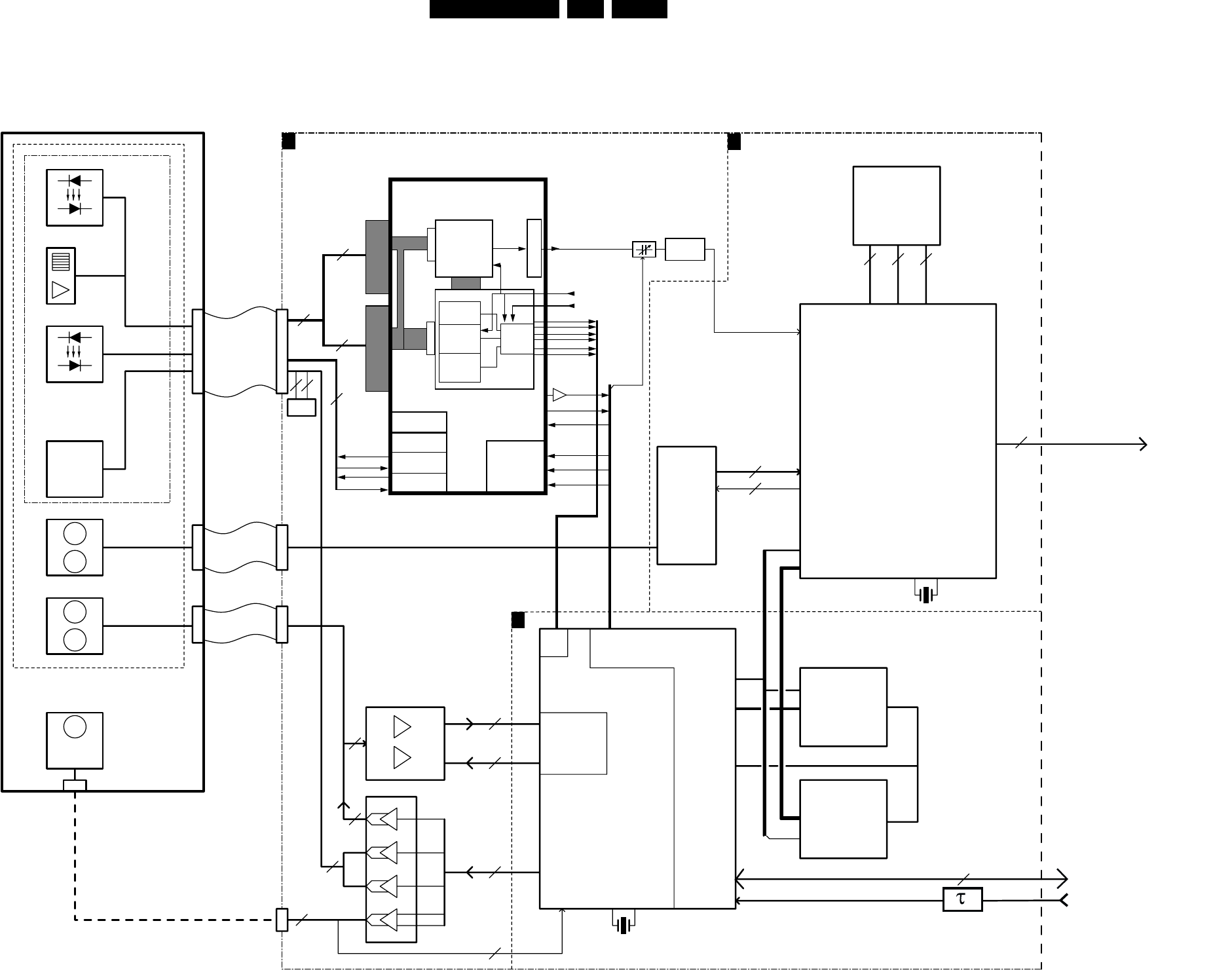
Block diagrams 29ASD-1 6.
6. Block diagrams
Servo
DISK MOTOR
SLEDGE MOTOR
TRAY MOTOR
6 MHz
8.46 MHz
LM833D
uP (8051 CORE)
ADC
7207
SAA7399
MACE2
SERVO
B_V4
B_SYNC
B_FLAG
B_DATA
B_BCLK
B_WCLK
6
SAA7335HL/E/M2
HD61
DECODER
HF-IN
3
7304
BA6856FP
MOTOR-IC
HALL-FEEDBACK
DRIVE
MOTO-IN
TACHO-OUT
LOADER
CDM
OPU
DVD-LASER
CD-LASER
RADIAL
FOCUS
M
HALL
M
HALL
M
END-SWITCH
4-WIRES
FLEX 24P
FLEX 11P
FLEX 8P
PCS-PRE-AMPL
DRIVERS
7104
7103
4
2
4
4
2
4
+5 GND
PCS
PHI-INPUT
REF
BA5938FM
SERVO OUTPUTS
TRAY-SWITCH
SLEDGE
RADIAL
FOCUS
TRAY1
TRAY2
5
2
2
CONTROL
LINES
1104
1106
1301
1100
1
1
7311
CONTROL BUS
DATA/ADDRESS BUS
AD[0:7]AD[0:7]
A[8:16]
A[0:16]
A[0:7]
AD[0:7]
AD[0:7]
PSENN
FLASH ROM
ADRESS LATCH
7202
7201
MEMORY
132K
S-RAM
DATA
ADDRESS
CONTROL
815 1
4268_136
2012
Laser#1
Laser#2
Diode
Amplifiers
Processing
DPD
Land/Groove
Swap
Dual Laser
Supply
Serial
I/Face
Push Pull
3 Beam
Tracking
Var Gain
Servo
Signals
DVD
CD D1-D6
MUX
CALF_MACE
O_CENTRAL
Land
V & I references
Header
Offset Mute
compensations
MUX
SILD
SICL
SIDA
4
6
4
6
TO STi5505 ON DIAGRAM 5
DVDALAS2+
TZA1033
RFo
STB_DALAS
ASD1 BOARD SERVO PART
7310
7102
CY7C199-15C
AM29F002
74HCT573D
BLOCKDIAGRAM DIGITAL PART
TXD_BE
RXT_BE
CFR
SUR
4
TO/FROM STi5505 ON DIAGRAM 5
S2B
I2S
HPSW
EQUALIZER
7110-7111 7100-7106-7101
RSTN
POR
13
2
CL06532065_036.eps
180500
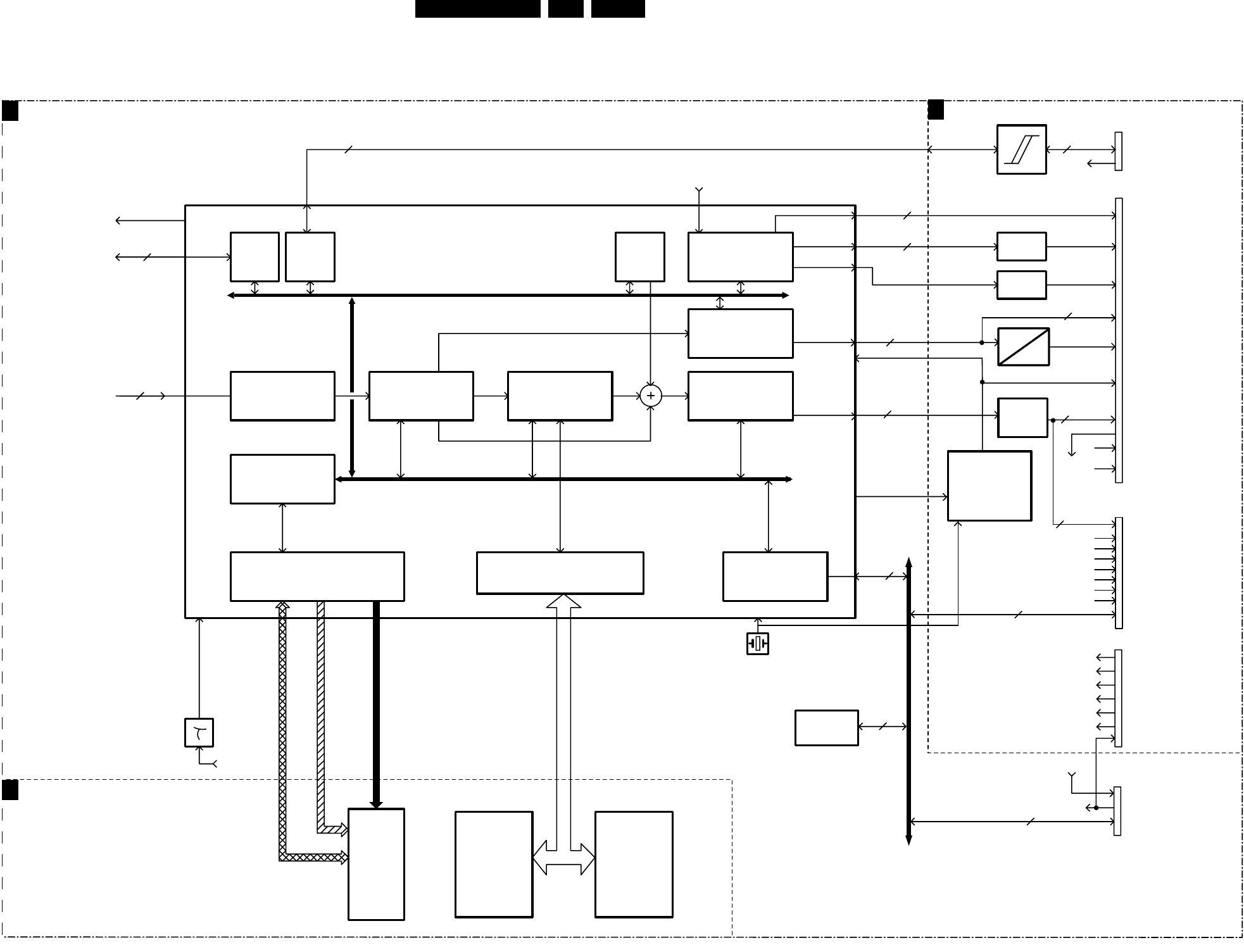
30ASD-1 6.
Block diagrams
Didital
7504
ST24E32M6
7505
7612-7618
7611
SERVICE
RESETN
-8Vstby
7600
7503
STi5505
SERVICE
4
I/O
OSD
DECODER
ENCODER
CONTROLLER
I2CSDRAM CONTROLLER
PROGRAMMABLE
VIDEO
AUDIO
MPEG DECODER
DEMULTIPLEXER
MEMORY INTERFACE
HOST
ST20
UART UART
INTERFACE
FRONT END
16Mb
B_SYNC
B_FLAG
B_BCLK
B_DATA
B_WCLK
B_V4
1501
STB_CONT
AM29LV160BT
7401
MK2742
7616
SEL_ACLK
CTS_SER
RTS_SER
RXD_SER
TXD_SER
4
SUR
CFR
RXD_BE
TXD_BE
S2B
4
I2S
6
1602
1600
TO/FROM
DISPLAY
BOARD
A/V-MUX
INTERFACE
SERIAL
SUPPLY
POWER
STB_CONT
+6Vstby
+5Vstby
+5V
+3V3
SYNTHESIZER
FLASH
CLOCK
27 MHz
1603
MUTE
MUTE_AV
SCART
0_6_12V
DEEM[0:1]
P50
6
-5V
+5V
R/C
G
B/CVBS
CVBS/Y
TO/FROM
CONN.
CONN.
CONN.
CONN.
0/6/12V
SERVICE
+12Vstby
7608,7609,7610
7604, 7607
AUDIO
VIDEO
SUBPICTURE
3V3
5V
VIDEO
FILTER
BUFFER
2
4
SCART[0:1]
MUTE
SCLK
PCM_OUT0
PCM_CLK
LRCLK
SPDIF_OUT
R_OUT
G_OUT
B_OUT
C_OUT
CVBS_OUT
Y_OUT
2
4
3
1604
CONN.
BOARD
A/V-MUX
TO
2
OPTION
+12Vstby
+3V3
+6Vstby
-8Vstby
HSYNC
PCMout1
PCMout2
Y - C
EEPROM
DIG_OUT
BCLK
DATA
ACLK
WCLK
SDA
SCLK 2
2
2
2
SDA
SCLK
SCLK
SDA
7405
SDRAM
7404
MT48LC1M16A1TG -7S
16Mb
SDRAM
16Mb
SDRAM INTERFACE
SYSTEM DATA BUS
SYSTEM ADDRESS BUS
SYSTEM CONTROL BUS
CVBS
RGB
S-VHS
DIG. OUT
PCM (3X)
I2C
4268_136
2012
TO /FROM
MACE2
(DIAGRAM 2)
FROM
HD61 DECODER
(DIAGRAM 3)
ASD1 BOARD DIGITAL PART
P50
PCM__CLK
MT48LC1M16A1TG-7S
RSTN
5
4
6
CL06532065_037.eps
180500
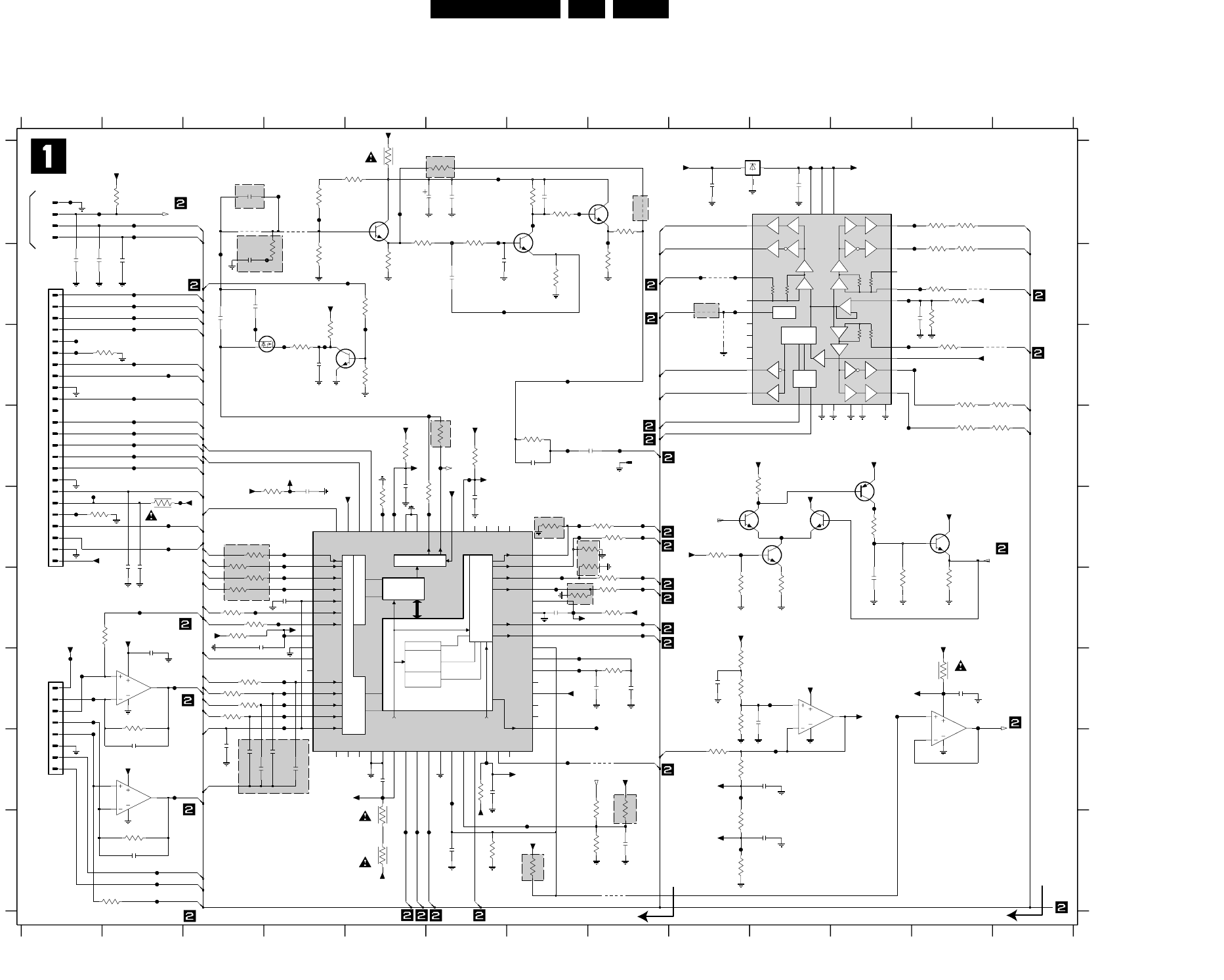
Electrical diagrams and PWB’s 31ASD-1 7.
7. Electrical diagrams and PWB’s
SERVO DALAS
X2
+
+
+
+
-
X2
X2
MT
X2
X2
X2
X2
X2
MUTE
VOLTAGE
CONTROL
LOGIC
TRAY
-
-
-
MUX
VAR GAIN
LAND/
GROOVE
SWAP
MUTE
LAND
MUX
DPD
PUSH PULL
OFFSET
COMPENS.
3 BEAM
TRACKING
DIODE
AMPLIFIERS
PROCESSING
HEADER
3115 B12
F131 C33149 E8
12 13
F159 E8
F160 E2
F021 F7
F119 B9
3119 B7
F036 E9
2143 B1
2116 E4
9
3148 G9
F154 E2
F180 G4
F181 G1
F152 D6
3129 C5
3191 B9
3192 B12
234
3135 D5
3180 I2
F117 B3
TO / FROM LOADER
3151 E3
F162 E4
F163 H10
3183 F10
3184 I6
3185 I5
F120 B12
F121 B2
F128 C2
F129 C5
F130 C1
3178 I5
F013 I23101 A6
3125 C4
A
3188 A8
3
3144 E1
5
3146 E8
3147 E8
F183 G4
F118 B9
F197 G11
F022 G12
F023 H5
F024 H6
F035 E9
E
F167 F4
3126 C4
3181 I8
3128 C2
3138 G9
3130 C12
3131 C13
2129 G8
F147 D2
F039 E11
7106 A7
F177 G1
F178 G7
F155 E7
F156 E8
F017 E5
2130 H2
2131 H3
3143 G9
3136 D6
3145 E7
3197 C9
3137 D6
F116 A2
F112 A6
F198 G12
F199 I7
F164 F4
F165 F7
F166 F8
7104-B H2
F111 A2
F169 F8
3182 F10
F171 F3
3139 E4
3140 E5
3193 C13
3194 H8
3195 I8
F192 H2
F101 A10
2103 A5
2104 A6
2105 A7
F189 G8
F190 H1
2100 A9
3150 E3
TO / FROM LOADERTO LOADER
2133 H4
2134 H3
3198 D10
3120 F12
2138 H6
F014 B4
F015 E4
F016 F4
3100 A5
12 13
F144 D2
3113 B4
7114 E10
2118 G9
2119 G10
3141 E2
2107 B6
3142 E5
2113 D8
2114 D7
7110 C4
7111 C5
7112 E10
F135 C1
2108 B6
F179 I9
F132 C4
F133 C11
F153 E2
3122 B12
3123 B5
3124 B12
3179 E11
3187 I2
3127 C12
3189 A3
7104-A G2
B
F168 F7
D
F170 F2
F
F109 A7
3177 H8
3132 D12
3133 D13
3134 D7
F143 D2
4
2115 D5
67
3171 G3
3172 G2
7113 E10
F110 A1
1
2106 B3
7115 D11
F107 A4
8
78
2135 H4
2136 H5
2137 G12
F157 G10
F158 E7
F011 I2
3199 E9
F037 E10
7101 A8
F150 E1
3173 F12
3112 A6
F186 G4
3114 B12
F184 G1
F185 G4
F122 B5
F123 B11
F124 B2
1105 D8
1106 G1
3190 A4
2127 I10
3166 G8
1
3168 I9
F137 C12
2110 B3
F139 C7
F018 E5
91011
I
F182 G2
F019 D6
F020 D6
3164 F3
3165 I9
F172 H9
F038 E11
F173 F4
3174 G12
3175 H6
F
3121 B12
F127 B2
3116 B4
3117 B5
F161 E4
F125 B6
F126 B9
F191 H7
2102 A3
F194 I5
F195 I5
3153 H9
3154 F3
7105-A G12
7105-B G10
2141 I2
2101 A10
2117 E6
3102 A5
3103 A4
G
H
2144 B2
2145 B2
3118 B8
5
3167 G3 F149 E2
F148 D2
1100-1 A1
1100-2 A1
3155 F8
F187 G1
F188 G4
F145 D7
F146 D8
2121 E2
2122 F4
A
7109 A9
2128 G8
3152 E8
2132 H3
6
F141 D2
F142 D12
2142 F11
3176 H8
F136 C2
3104 A7
F196 I5
E
F113 A6
F114 A8
F115 B12
7103 A10
2140 I6
D
F175 F8
2120 E2
2139 I8
10 11
1100-3 A1
G
H
I
2111 B11
2109 B3
C
F174 F8
3170 G3
1100-4 A1
1104 B1
F193 H6
3186 I7
2123 H10
2124 F7
2125 G3
2126 G2
3157 F8
F176 G7
F102 A6
F103 A4
F104 A7
F105 A1
F106 A5
F134 C4
OPTION
OPTION
OPTION
3156 F3
3106 A7
3107 A12
2
F012 I2
3159 F7
F151 E5
3161 F8
3162 F3
B
C
7116 E12
3105 A2
3158 H9
3108 A12
3160 F3
3110 A8
3111 A5
3196 B9
2112 C4
F108 A12
F138 C2
7100 A5
F140 C2
7102 E4
3169 G3
3163 F1
OPTION
OPTION
OPTION
OPTION 1
OPTION
OPTION
OPTION
OPTION
OPTION
OPTION
F036
F158
BC847B
7112
F037
3104 123 4268.4
PB 4268 ASD1
MONO-BOARD
+5V
2118
22n
3151
F118
F199
100R
3198
2135
15p
15K
3176
470R
F137
47R
3136
68K
3177
3199
3133
2R2
3171
10K
3196
12K
3152
100R
3
4
5
6
7
8
52271-XX90
1106
1
2
+5V
F144
7100
BFS20
+5A3
1R
3139
47R
3112
10K
3147
1100-2 2
F103
F145
220p
2143
F189
2.5V
100R
3183
2100
100n
+5V
F106
F129
3
2
220p
2145
F101
BFS20
7106
1
120R
3165
F120
F151
F149
10K
3105
220R
3179
47R
3140
3120
1K
F173
+5V
F015
3192
F116
10n
2142
150R
3111
1K
3182
F196
F178
F022
+5D
100n
4n7
2104
2120
2128
180p
+5A2
4R7
3141
2139
100n
3160
100R
F122
3173
F181
2111
100n
100K
F115
2R2
3131
39K
3166
+5V
F179
330R
3168
F192
F174
5
6
7
8
4
F177
F155
7105-B
MC34072
+5V
+5V
2123
100n
F160
F023
F117
F150
F014
F183
+5V
+12Vstby
2140
330p
+5V
3194
3122
470R
100R
3158
10K
3123
+5V
+5V
2138
22p
2141
1105
100n
3107
2R2
+12Vstby
2137
100n
F104
+3V3D
7113
BC847B
F148
F011
BC847B
7114
5
6
7
8
4
3135
2R2
2144
220p
LM833D
7104-B
22K
3148
F142
+3V3S
3190
F180
2117
100n
2.0V
3130
F167
22p
2106
2R2
VREF
10K
3125
+5A1
10
VCC2
21
VCC3
3
VIN1
4
VIN2
VIN3
20
24
VIN4
25
VIN5
12
VO2+
13
VO2-
18
VO3+
17
VO3-
VO4+
26
27
VO4-
2
VOL+
1
VOL-
19
23
BIAS
16
FWD
8
GND1
14
GND2
28
GND3
29
MT1
30
MT2
MUTE
7
5
NC1
6
NC2
9
NC3
11
NC5
15
REV
22
VCC1
1100-4 4
BA5938FM
7103
F113
3149
F102
+5V
12K
2127
100n
F161
F162
F111
F156
F013
3162
100R
220R
3143
3117
1100-3 3
3191
180R
F153
F039
F024
F154
F152
+5V
2126
100n
+3V3S
100R
3169
F166
BC857B
7115
3127
22K
2116
100n
F176
100R
+5V
6K8
3138
3154
F134
3145
12K
560R
3181
2109
1n5
F019
F163
10K
3155
F185
3
2
1
8
4
+5V
3195
F012
LM833D
7104-A
22p
2130
F110
F124
2121
220n
3172
100K
100R
3170
3189
3188
F197
330R
3134
7109
L78M09
GND
2
IN
1
OUT
3
3132
2R2
F136
390R
3119
+5A4
F126
+5Vx
F127
4
3180
100K
MC34072
7105-A3
2
1
8
47R
3110
2113
100n
F198
F159
3113
8K2
BC847B
7111
F119
2131
22n
7116
BC847B
F182
F038
F035
F195
1K5
3102
2108
390p
47R
3106
F021
3129
3K9
F017
91R
3144
F165
27K
3187
2115
100n
F146
F147
10K
F132
F194
3157
F143
TM
19
VDDA18
VDDA2
59
VDDA3
53
VDDA4 44
VDDD3
22
VDDD5
30
VDDL
63
VSSA19
VSSA2
58
VSSA3
57
VSSA4 43
VSSD
26
27K
3163
O-C 46
O-CENTRAL 40
O-D 45
R-EXT
60
RF-REF
54
RFN
56
RFP
55
S1 42
S2 41
SICL
24
SIDA
23
SILD
25
STB
31
TD1 35
TD2 37
TDO 34
HEADER
21
LAND
20
LPF-DPD1 38
LPF-DPD2 39
NC111
NC2
17
NC3
18
NC4
32
NC5
49
NC6
50
NC7
51
NC8
52
O-A 48
O-B 47
61
CD-MI
62
CD-REF5
COM
28
COO
29
COP
27
DVD-A12
DVD-B13
DVD-C14
DVD-D15
DVD-LO
64
DVD-MI10
DVD-REF16 FTC 33
FTC-REF 36
7102
TZA1033
CD-A1
CD-B2
CD-C3
CD-D4
CD-E6
CD-F7
CD-LO
+3V3S
F186
F138
+5Vx
+9V
+5L
F016
3126
10K
3121
+5V
F140
27K
10M
3186
3197
1.5V
680R
3118
F139
F107
F105
2.0V
1K5
3103
22
23
24
3
4
5
6
7
8
9
+3V3S
F133
1
10
11
12
13
14
15
16
17
18
19
2
20
21
F175
1104
15p
2133
12K
1.5V
F141
F109
3142
100R
F130
F125
3156
3185
1R
2103
47u
1100-1 1
F184
F121
7101
BFS20
13
2
F191
1R
3178
3101
47R
3193
10K
3146
3167
100R
F135
F131
F123
F190
F114
2101
100n
F018
2R2
3137
2112
1n
390R
3104
3K9
3116
3184
120K
3115
2R2
F157
2107
68p
F168
2105
22p
2110 2n2
2114
100p
2129
100n
2136
1.5V
+5L
180p
3164
2R2
F188
F169
3114
2R2
+5V
F108
2R23175
3128
91R
F187
7110
BST82
F170
15p
2132
F128
100R
3150
47p
2102
F172
470R
3124
3161
2R2
+5V
2.5V
2119
22n
F020
2122
22n
F171
4R7
3174
2134
15p
4R7
3100
F193
+9V
3108
2R2
F112
2124
100n
22R
3153
F164
12K
2125
100n
SL-
SL+
3159
SICL
SIDA
SILD
RAC-SW
RFP
A1_MACE
ALPHA0
CALF_MACE
LDCD
MON1
O-CENTRAL
LD-DVD
RFP
S1
S2
SINPH
V-REF
F
E
VO2+
RFo
RAD+
RAD-
LDCD
RAD-
FOC+
LD-DVD
FOC-
V-REF
E
F
D
C
B
Ax
RAD+
SL-
SL+
VO2-
TRAY2
TRAY1
HPSW
COSPH
O1
O2
C
B
C
B
V-REF
MON2
TRAYSW
FO
RA
VO2-
VO2+
REFCOS
REFSIN
SL
FOC-
FOC+
MON1
MON2
03
04
Ax
D
Ax
D
V-REF
STB_DALAS
RAD-
RAD+
FOC-
FOC+
SL-
SL+
VO2-
VO2+
V-REF
CL06532065_038.eps
180500
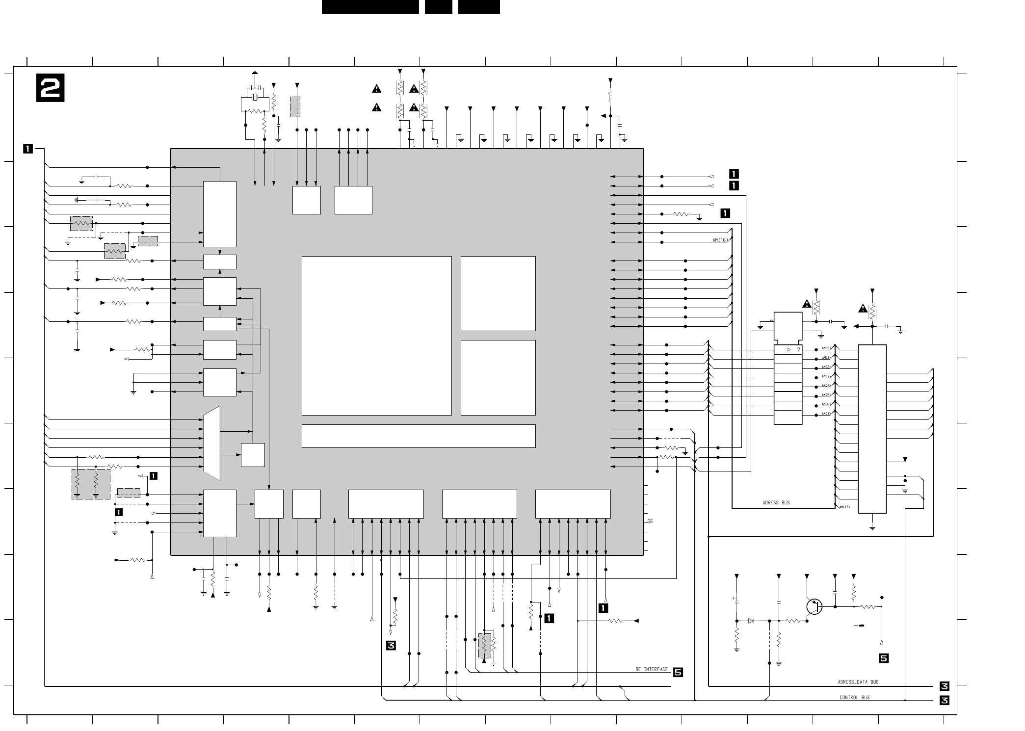
32ASD-1 7.
Electrical diagrams and PWB’s
SERVO MACE
EN
C1
1D
core
8051
SFR
RAM
ROM
ref.
AGC
ADC/
Laser
control
control
Slegde
control
Port 5 Port 3
Port
Port 1
GEN.
TEST
DEBUG
4
Port
2
0
Port
System
interface
P6
CLOCK
PCS
counter
Radial
Focus
Track
Defect
Signal
cond.
Ex
Dx
OPC
control
detector
2213 H4
2214 H13
F220 C2
F221 C2
F242 E13
F243 E10
4
3211 D2
3210 C2
3202 A7
3203 A4
C
12
2216 H12
2226 A4
2227 A6
2228 A7
7
2209 D14
F268 H8
F269 H7
3206 B2
3227 H13
3228 I8
3229 H13
3212 D13
F200 A5
F201 A5
3250 G2
3205 B2
3204 A4
3208 C2
F027 G2
F026 G2
F240 D13
F241 E10
3230 H8
3231 H6
3232 H12
3240 B10
3241 B1
3254 H8
3251 H8
3252 H8
3253 H5
3209 C2
2210 D1
2212 H3
F289 I7
F290 I7
F291 I6
F292 I6
2215 H11
3215 D2
3214 D2
5
F276 H6
F277 H6
F278 H4
F255 F10
F256 F10
F257 F11
F258 F2
F259 F11
1201 I13
1205 A4
2203 A10
2204 B2
3200 A4
3201 A6
F266 H9
F267 H8
F254 F10
F271 H8
F272 H9
F273 H5
3
F212 B10
F213 B2
6
F262 F10
F263 G2
F264 H4
F265 H3
F025 G2
F032 H8
F031 I8
3213 D14
F208 A5
F209 A6
F210 A5
F202 A9
F203 A6
F204 A4
F205 A7
F028 H4
8 9 10 11
F216 B10
F217 B2
F218 C10
F219 C10
F222 C11
F284 H8
F285 H13
F286 H12
F244 E13
F245 E10
F214 B10
F215 B2
F230 D2
F231 D11
F232 D11
F233 D1
F293 I8
F294 I12
F274 H5
F275 H5
F238 D13
D
F279 H4
F280 H6
F281 H14
F248 E13
F249 E10
3219 F2
3220 F10
2205 B2
2206 C1
2207 D1
2208 D13
2
F223 C11
F224 C2
F225 C11
F299 B2
F239 D10
F260 F14
F261 F2
10 11 12 13
F246 E13
F247 E10
F270 H9
F207 A6
D
E
F
F211 A4
F250 E2
F251 E13
F252 E10
F253 E13
7207 A3
3246 C2
3247 F10
F206 A5
12 13 14
1
3225 H5
345
F287 I11
F288 I12
F228 C11
F229 D11
3236 H9
3237 H2
3238 I8
3239 F10
F295 I7
F296 I7
F297 A4
F298 A10
3259 A6
3260 A7
5200 A9
6200 H12
7201 D12
7202 D13
14
A
B
C
3242 C1
3243 C2
3221 F2
3222 F1
3223 F2
3224 H3
3245 A5
H
I
3248 G2
F226 C1
F227 C2
89
OPTION
3244 C2
E
F282 H7
F283 H7
H
I
3249 G2
F029 H5
F030 I8
3255 I7
3256 I7
3257 I8
3258 I12
7203 H12
F234 D2
F235 D11
F236 D2
F237 D10
3226 H4
G
F
G
A
B
F033 D13
F034 D13
67
3234 I11
3235 I12
1205
CSTCC
OPTION
OPTION
OPTION
OPTION
OPTION
+3V3S
2K7
6200
BAS316
F242
3208
F213
3211
4K7
11K
3222
F292
2206
33n
10K
3220
10K3238
+3A
F298
F258
3224
150R
F236
F299
F028
F026
F250
+3V3S
F240
+5V
+5VC
F288
F287
2215
22u
+5V
F232
+5V
F221
F278
3213
4R7
F276
+3A
F226
3249
10K
3239
F296
F297
F218
+3A
F285
F243
2210
1n
F274
100n
2205
F208
3221
10K
F295
F200
2214
22n
1201
F291
3254
F225
10K
3219
+3V3S
F202
F235
F239
+3V3S
100n
2228
3259
1R
F275
2227
100n
F233
F230
F261
3245
F272
3258
F259
+3A
F280
F255
F212
F260
F283
+5VC
1R
3202
100n
2212
3257
F256
F265
F267
F222
12K
3229
8K2
3234
2R2
3232
4K7
3227
1n
2216
+3V3S
F254
F031
3203
1M
F224
3256
100MHZ
2203
100n
3240
10K
5200
F207
1R
3260
714
813
912
11 10
GND
120
Vcc
F205
74HCT573
7201
219
318
417
516
615
F245
F234
+3A
2208
+3V3S
3250
F216
100n
10K
3206
F210
F229
F215
F241
10K3228
F286
3214
3K9
3210
3K9
+3V3S
F219
F284
F289
F253
3212
4R7
F214
+3A
F030
F204
+3V3S
F029
F223
+3V3S
F027
+3A
F025
F228
3253
3200
10K
3246
3252
+3A
F266
F279
F294
F271
10K
3237
2213
100n
+3V3S
F277
F201
+5V
F246
F211
2204
100n
F220
F268
BC857B
7203
+3V3S
3255
+3V3S
F033
F247
+3A
3251
F269
3223
11K
F273
3215
10K
F217
F264
2226
100n
F293
+3A
3209
4K7
F203
F238
10K
3230
100n
2209
200K
3225
3204
330R
100K
3235
F290
F237
3248
F248
F251
F244
F206
+3V3S
3242
22K
3244
F231
3236
4K7
W_
F249
A7
27 A8
A9
26
13
DQ0
14
DQ1
15
DQ2
17
DQ3
18
DQ4
DQ5 19
DQ6 20
21
DQ7
22
E_
24
G_
RP_NC 1
32
VCC
16
VSS
31
12 A0
11 A1
23 A10
A11
25
4A12
28 A13
29 A14
3A15
2A16
30 A17
10 A2
9A3
8A4
7A5
6A6
5
F034
7202M29F002
F282
3201
1R
F032 F281
3247
F257
F262
3205
10K
3241
22K
3243
VssDc1
82
VssDc2
21
56
VssDp1
VssDp2
95
VssDp3
43
VssDp4
31
VssDp5
11
VssDp6
68
41
WRN
WRNH
19
127
XDET
XTLI
7
XXTLO
6
+3V3S
TXD2
40
Uopb
118
117
Uopt
VRH
105
VddAop
120
VddAs
110
VddDc1
83
VddDc2
22
57
VddDp1
VddDp2
96
VddDp3
44
VddDp4
32
VddDp5
12
VddDp6
69
VssAop
119
VssAs
109
33
39
RXD2
S1
112
S2
113
SELPLL
5
125
SINPHI
SL
72
SRV_INT_LGR
89
TEN
85
TL_FTL
81
84
TPWM
TS1
99
TS2
102
TS3
103
TXD1
34
79
P6
104
PSENn
53
PW
124
PXT0
17
PXT1
18
16
PXT2
PXT2en
15
RA
70
RAC_SW
10
RDN
42
20
RDNH
9
REFCOS
8
REFSIN
RP
80
RSTI
98
RXD1
13
INT3|ALEh
14
IREFT
114
LDON
97
LLP
94
MON_A
74
MON_D
73
2
NC1
3
NC2
NC3
36
NC4
37
NC5
NC6
67
NC7
100
NC8
101
88
OPC_INT
OTD
FOK
87
FTCH
115
FTCL
116
H0|A16
23
24
H1|A17
H2|CSDN
25
H3|CSBN
26
H4
27
28
H5
H6
29
H7
30
I2CSCL
90
I2CSDA
91
35
INT0_PWD
INT1
38
INT2
ALPHAO
4
ATIPin
77
CALF
123
CLKOUT
76
CLO
86
126
COSPHI
D1|MIRN
106
107
D2|TLN
D3|REN
108
111
D4|FEN
DEB_OUT
75
DEFIn
92
DEFOn
93
DSDen
78
EAn
55
FO
71
A2
122
A8
45
A9
46
1
ACT_EMFN
128
ACT_EMFP
AD0
58
AD1
59
AD2
60
AD3
61
AD4
62
AD5
63
AD6
64
AD7
65
ALE
54
7207
SAA7399HL
A1
121
A10
47
A11
48
A12
49
A13
50
A14
51
52
A15
F227
F252
F209
F263
3226
10K
1n
2207
F270
WE
RSTN
3231
10K
S2
RAD-
RAD+
A1_MACE
PSENn
AM(14)
AM(13)
AM(12)
AM(11)
AM(10)
RAC-SW
ALPHA0
POR
ATIP_IN
S1
O2
O1
COSPH
PORN
CALF_MACE
ALE
AMD(7)
AMD(6)
AMD(5)
AMD(4)
AMD(3)
AMD(2)
AMD(1)
AMD(0)
AM(9)
AM(8)
AM(15)
INT
O-CENTRAL
SILD
SICL
OTD-HD61
TRAYSW
CSI
AM(17)
STBY
p93-89
04
03
TRAY1
p93-89
SINPH
SUR
TXD_BE
POR
HPSW
STB_DALAS
ATIP_IN
T1
AM(0:17)
AM(0:17)
AMD(0:7)
{ALE,PSENn,RDI,WRI,CSI,WE,OTD-HD61,POR,PORN,RSTN,INT,MOTO1,RFo,T1,T2,T3}
+3A
p93-89
SIDA
CFR
RXD_BE
TRAY2
AM(7)
AM(8)
AM(9)
AMD(7)
AMD(6)
AMD(5)
AMD(4)
AMD(3)
AMD(2)
AMD(1)
AMD(0)
AMD(0)
AMD(1)
AMD(2)
AMD(3)
AMD(4)
AMD(5)
AMD(6)
AMD(7)
{CFR,SUR,RXD_BE,TXD_BE}
FO
RA
SL
REFCOS
REFSIN
+5V
PSENn
WRI
RDI
WE
RFo
ALE
AM(0)
AM(1)
AM(10)
AM(11)
AM(12)
AM(13)
AM(14)
AM(15)
AM(16)
AM(2)
AM(3)
AM(4)
AM(5)
AM(6)
3104 123 4268.4
PB 4268 ASD1
MONO-BOARD
H2
I6
H9
E2
E2
CL06532065_039.eps
180500
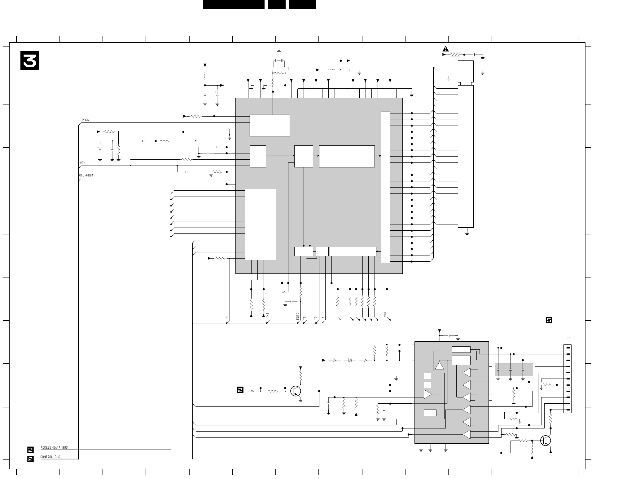
Electrical diagrams and PWB’s 33ASD-1 7.
Decoder
CLOCK
GENERATION
CONTROL
ANALOG
DATA
CAPTURE
SUB-CPU
INTERFACE
MOTOR
INTERFACE
TACHO
BLOCK
SERIAL OUT
INTERFACE
DETECTOR
BIT
DETECTOR DEMOD
-+
REV
PS
-
+
H BIAS
CONTROL
GAIN
DRIVER
+
-
+
-
+
+
-
+
-
+
-
+
-
F336 F7
F337 F7
F364 H12
F315 C10
11 12
2310 G11
2309 F7
F349 G9
F350 G12
3302 A7
3304 B3
3305 C3
3309 C5
F344 F8
F365 I13
7310 A10
4
13
C
3
F329 D10
3334 F8
F371 I9
F372 I12
3337 F9
3338 F9
F340 F6
F341 F7
3300 A11
3301 A6
21
3310 E5
F338 F8
F351 G9
F343 F9
F342 F9
7304 G11
6303 G8
56
7312 I13
7315 H7
F325 D10
3329 I13
3330 B5
F312 B4
8
2304 B5
3316 G9
F316 C5
10
3319 H13
3320 H6
2312 H12
2311 H12
3323 H8
11
H
I
A
B
910
5300 A8
5301 A5
F332 E10
F333 E10
F334 E10
F335 E10
F369 I13
2305 C5
2306 C2
2307 C3
F352 G12
F313 B10
3331 B4
3332 C4
F366 I12
12
F309 B4
3313 F6
D
F327 D10
2319 C4
F308 B10
3335 F8
3336 F8
F305 B10
7
3339 C5
3340 H9
1300 A6
1301 G13
F363 H9
F367 I12
F368 I9
F319 C5
F320 C10
F321 C10
F322 C5
F323 C10
E
F326 D10
2313 H12
3324 I9
F346 F8
F356 H13
F317 C10
2302 A5
2303 A5
B
C
3317 G9
3318 H7
3312 F6
3325 I12
3321 H12
3322 H8
H
I
3328 I12
65
F300 A11
F301 A8
F302 A7
F303 A5
F304 A6
13
1234
F370 I12
2314 H8
F339 F6
F347 F9
F348 F8
F361 H9
F362 H8
F311 B10
F310 B10
E
F
2315 I9
2318 B3
G
FF307 B10
F306 B5
G
F328 D10
8F353 G12
F354 H12
F355 H9
6301 G8
6302 G9
7
3333 F8
F314 B5
9
2300 A11
2301 A8
TO LOADER
7311 A6
F373 I12
F324 D10
F345 F8
NOT MOUNTED
F318 C10
A
D
3311 F7
3326 I13
3327 I12
F330 D10
F331 E10
F357 H6
F358 H7
F359 H12
F360 H8
58
46 WRI
+5VB
F342
F346
81
VDDD7
92
VDDD8
98
VDDD9
5VREF
1
VSSA1
7
VSSA2
11
VSSD1
20
VSSD2
VSSD3
32 45
VSSD4
60
VSSD5
73
VSSD6
82
VSSD7
93
VSSD8
99
VSSD9
WCLK
50
STOPCLK
54
SYNC
18
T1
17
T2
21 TEST1
22 TEST2
52
V4
VDDA1
100 9
VDDA2
10
VDDD1
19
VDDD2
31
VDDD3
44
VDDD4
59
VDDD5
72
VDDD6
84RAD8
85RAD9
71RDA0
70RDA1
68RDA2
67RDA3
66RDA4
RDA5 65
64
RDA6
63RDA7
47 RDI
4REFHI
3REFLO
61RRW
29
SCL
28
SDA
12 OTD
23 PORE
74RAD0
75RAD1
87RAD10
88RAD11
RAD12 89
90
RAD13
91RAD14
76RAD2
77RAD3
78RAD4
79RAD5
80RAD6
83RAD7
IREF
2
97
MEAS1
13
MOTO1
15
MOTO2|T3
24 MUXSW
14 NC1
86
NC10
16 NC2
25 NC3
36 NC4
NC5
38 42
NC6
51
NC7
62
NC8
69
NC9
CRIN
9495
CROUT
49 CSI
43 DA0
41 DA1
40 DA2
39 DA3
37 DA4
35 DA5
34 DA6
33 DA7
56
DATA
53
EBUOUT
55
FLAG
6HFIN
30
INT
SAA7335HL
7311
8AGCOUT
48 ALE
BCAIN
27 57
BCLK
96
CFLG
26
CL1
+5VB+5VA +5VB
F327
22n
2305 22n
2304
+5V
F321
F316
1M
F336
+5VB
2306
10u
3301
+5V
3313
4K7
3339
4K7
3312
+5V
+5VA 11
I|O1
12
I|O2
13
I|O3
15
I|O4
16
I|O5
17
I|O6
18
I|O7
19
OE_
22
28
VCC
WE_
27
100n
2300
6
A11
7
A12
8
A13
9
A14
10
A2
24
A3
25
A4
26
A5
1
A6
2
A7
3
A8
4
A9
5
CE_ 20
GND
14
I|O0
F317
CY7C199
7310
A0
21
A1
23
A10
F318
F315
F305
F310
F347
22K
3330
F333
1R
3316
+5V
F308
NC2 2
NC3 4
6
NC4
NC5 15
PS23
REV24
RNF
28 VCC
25
VH19
VM1
26
VM227
+5V
EC22
21 ECR
FG1
18
FG217
FG316
GND
8
H1+ 9
H1- 10
H2+ 11
H2- 12
H3+ 13
H3- 14
MT1
29
MT2
30
NC1 1
+5VB
7304
BA6856FB
A1 7
A2 5
A3 3
CNF20
3300
4R7
+5VB
3325
6K8
2311
100n
F323
3340
+5VA
+5V
+5V
F313
BC857B
F341
2302
+5VA
7312
F354
+5V
100n
5301
47u
2303
F334
100MHZ
2K7
F370
22n
2307 3305
F330
F332
2K7
3304
F363
F331
+5VB
F325
F361
F329
100MHZ
22K
3311
F368
F324
5300
F301
F300
F357
F303
3320
4K7
F302
100n
2301
F309
F356
F314
+5VB
F352
F340
F345
+5VB
F344
100R
3333
3302
CSTCC
1300
2309
100n
220R
6301
3K3
3331
F335
+12Vstby
S1D
3310
6302
S1D
+5V
22K
100n
2310
6K8
3321
10K
3309
100n 100n
2313
F320
2312
3323
4K7
3337
100R
100n
2314
22K
F311
3328
22K
3329
+5V
F307
2315
100n
3319
47R
+5V
F343
F364
F366
F372
F367
F373
F328
F349
F351
F326
6303
F355
F358
S1D
4K7
F304
F306
3318
F369
F339
F365
100R
F350
100R
F348
3336
3332
3K3
3335
120p
2318
F322
F338
F312
F337
1R
3317
3327
6K8
7
8
9
52271-1190
1301
1
10
11
2
3
4
5
6
4K7
3322
F371
47R
3326
100K
3324
F359
F362
F360
7315
+5V
F353
BC847B
100R
3334
2319
27p
F319
100R
3338
RAMDA21
RAMDA11
RAMDA01
RAMAD91
RAMAD81
RAMAD71
RAMAD61
RAMAD51
RAMAD41
RAMAD31
RAMAD21
RAMAD141
RAMAD131
RAMAD121
RAMAD111
RAMAD101
RAMAD11
RAMAD01
RAMAD141
RAMAD41
RAMAD31
RAMAD21
RAMAD51
RAMAD61
RAMAD71
RAMAD81
RAMAD91
RAMAD11
RAMAD01
RAMRW
RAMDA71
RAMDA61
RAMDA51
RAMDA41
RAMDA31
T2
T1
RAMRW
RAMDA31
RAMDA41
RAMDA51
RAMDA61
RAMDA71
RAMDA21
RAMDA11
RAMDA01
RAMAD101
RAMAD111
RAMAD121
RAMAD131
AMD(2)
AMD(1)
AMD(0)
AMD(0:7)
ALE
RDI
WRI
B_WCLK
B_BCLK
B_DATA
B_FLAG
B_SYNC
B_V4
MOTO1
STBY
T3
MEAS1
AMD(7)
AMD(6)
AMD(5)
AMD(4)
AMD(3)
3104 123 4268.4
PB 4268 ASD1
MONO-BOARD
CL06532065_040.eps
180500
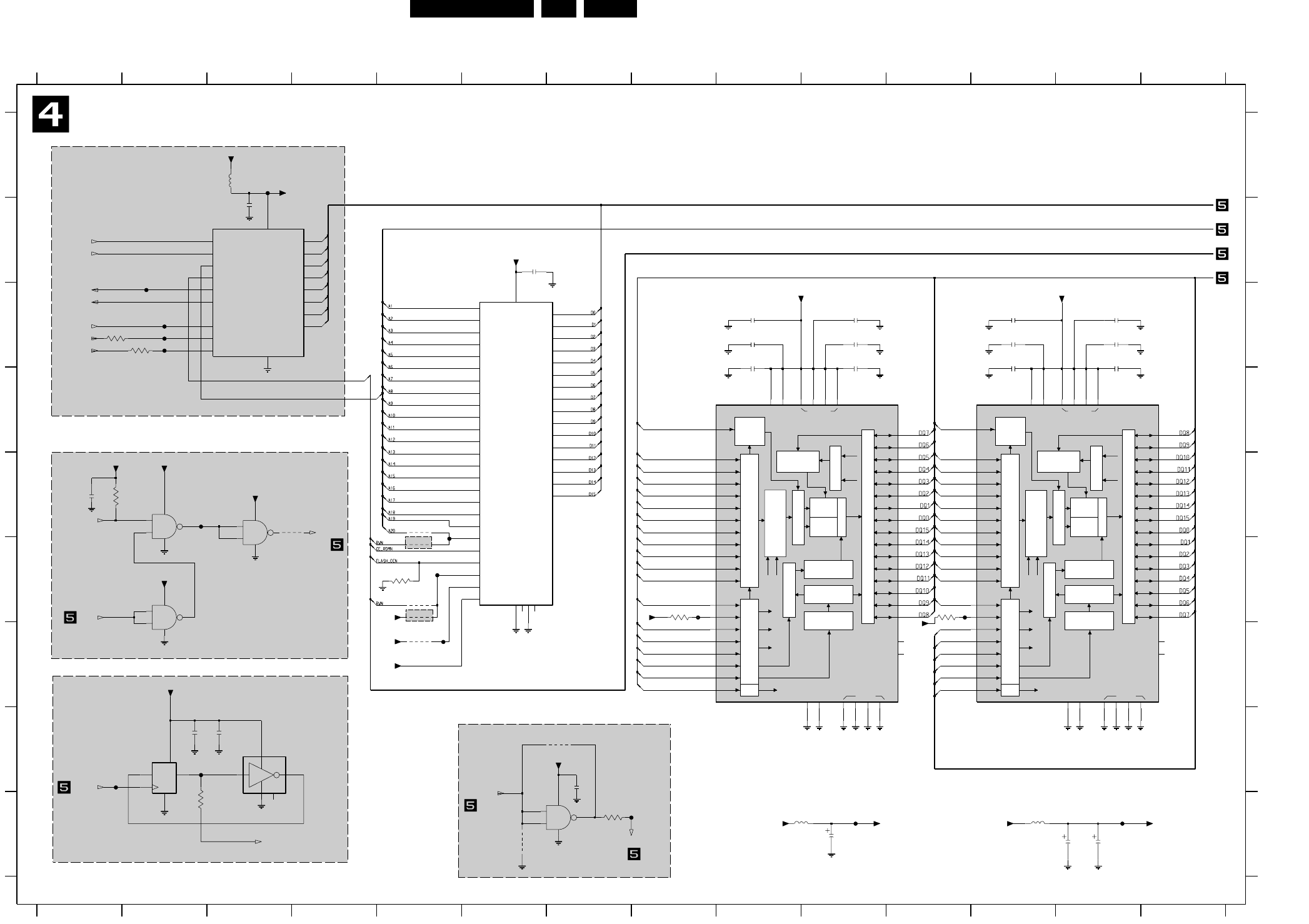
34ASD-1 7.
Electrical diagrams and PWB’s
Memory
VDDQ
LCBR
DATA INPUT
REGISTER
PROGRAMMING
LRAS
LCBR
512Kx16
BANK
SELECT
OUTPUT BUFFER
VSS VSSQ
TIMING REGISTER
NC
512Kx16
ADDRESS REGISTER
LCKE BURST LENGTH
LATENCY &
DECODER
COLUMN
LWCBR
LCAS
LWE
REGISTER
COL. BUFFER
LQDM
ROW DECODER
REFRESH COUNTER
ROW BUFFER
LDQM
LWE
I/O CONTROL
SENSE AMP
LRAS
VDD VDDQ
LCBR
DATA INPUT
REGISTER
PROGRAMMING
LRAS
LCBR
512Kx16
BANK
SELECT
OUTPUT BUFFER
VSS VSSQ
TIMING REGISTER
NC
512Kx16
ADDRESS REGISTER
LCKE BURST LENGTH
LATENCY &
DECODER
COLUMN
LWCBR
LCAS
LWE
REGISTER
COL. BUFFER
LQDM
ROW DECODER
REFRESH COUNTER
ROW BUFFER
LDQM
LWE
I/O CONTROL
SENSE AMP
LRAS
VDD
H
I
E
F
G
H
3412 E5
3413 F5
3414 F5
3415 F5
3416 G5
3418 E4
3402 E1
3403 F8
3404 F11
123
7400-A E2
7400-B F2
7400-C I6
78910
5400 A3
5402 I9
5403 I12
456
13 14
A
B
C
D
SDRAM Interface
789101112
F428 I8
F430 H2
F431 H1
F432 G5
F434 F5
F435 F5
SYSTEM DATA Bus
TOP
RAM/ROM Interface
2400 B3
2401 C9
2402 C10
2403 C12
I
A
B
C
D
E
F
G
3405 F5
3406 I7
3407 I3
3409 H7
3410 I6
2417 H3
2418 I10
2419 I13
2420 I13
3400 C1
3401 C2
OPTION
OPTION
7400-D E3
7401 C6
7402 H2
7403 H3
7404 D9
7405 D12
7406 B3
F406 E2
F415 G8
F416 G11
F419 I10
11 12 13 14
1
MEMORY PART
BOTTOM
SYSTEM ADDRESS Bus
23456
OPTION
OPTION
OPTION
OPTION
F420 I13
F421 A3
F422 C2
F423 C2
F424 C2
F425 C2
2404 C13
2405 B6
2406 C9
2407 C10
2408 C12
2409 C13
2410 C9
2411 C10
2412 C12
2413 C13
2414 H7
2415 E1
2416 H2
3404
10K
2410
100n 100n
2411
+5V_DS
VDD_MEM2
10K
3405
10K
3402
2417
100n
2401
100n
13 38 44
26 50 4 10 41 47
WE_15
VDD_MEM2
6
DQ4 8
DQ5 9
DQ6 11
DQ7 12
39DQ8
40DQ9
DQMH36
14 DQML
33
37
RAS_17
125 7
A8
32 A9
BA19
CAS_16
34 CKE
35 CLK
18 CS_
DQ0 2
DQ1 3
42DQ10
43DQ11
45DQ12
46DQ13
48DQ14
49DQ15
DQ2 5
DQ3
MT48LC1M16A1TG
7404
21 A0
22 A1
A1020
23 A2
24 A3
27 A4
28 A5
29 A6
30 A7
31
74HCT1G04
7403
2
3
NC
1
5
4
100n
2416
2408
100n
2400
100n
+5V_DS
5400
100MHZ
100n
2412
+5V_DS
22R
3407
74HCT1G79
7402
2
1
3
4
5
+3V3
+5V_DS
F430
100u
2418
+3V3
F424
+5V_DS
3418
F423 2404
100n
VDD_MEM2
100MHZ
5402
74HCT00D
7400-A
1
2
7
14
3
2414
100n
VDD_MEM2
+5VOSC
F431
F416
RD_
19
RESET_|STROBE_
3
SCL|SCL-IN
2
SDA|SDA-OUT
20
VDD
10
VSS
18
WR_
3401
100R
6
A0
1
CLK
17
CS_
7
DB0
8
DB1
9
DB2
11
DB3
12
DB4
13
DB5
14
DB6
15
DB7
4
IACK_|SDA-IN
5
INT_|SCL-OUT
16
VDD_MEM2
PCF8584T
7406
F415
100n
2403
100n
2402
3410
100n
2406
3409
VDD_MEM
+5Vstby
F434
100n
2405
VDD_MEM
F432
3414
3415
VDD_MEM
3413
74HCT00D
7400-C
9
10
7
14
8
3412
F419
100R
3406
F425
3416
41 47
15 WE_
39
DQ9 40
36 DQMH
DQML14
33
37
17 RAS_
1 25 7 13 38 44
26 50 4 10
35
CS_18
2DQ0
3DQ1
DQ10 42
DQ11 43
DQ12 45
DQ13 46
DQ14 48
DQ15 49
5DQ2
6DQ3
8DQ4
9DQ5
11DQ6
12DQ7
DQ8
A021
A122
20 A10
A223
A324
A427
A528
A629
A730
A831
A932
19 BA
16 CAS_
CKE34
CLK
7405
MT48LC1M16A1TG
F422
F421
100n
2415
100n
2409
DQ8
18
DQ9
14 OE_
1RESET_
23
VCC
13
VSS1
32
VSS2
44 WE_
BYTE_
12 CE_
15
DQ0
17
DQ1
20
DQ10
22
DQ11
25
DQ12
27
DQ13
29
DQ14
31
DQ15|A-1
19
DQ2
21
DQ3
24
DQ4
26
DQ5
28
DQ6
30
DQ7
16
A12
37 A13
36 A14
35 A15
34 A16
3A17
2A18
43 A19
9A2
8A3
7A4
6A5
5A6
4A7
42 A8
41 A9
33
Am29LV160BT
7401
11 A0
10 A1
40 A10
39 A11
38
F420
47u
2419
2413
100n
12
13
7
14
11
F428
+5V_DS
7400-D
74HCT00D
VDD_MEM
F435
100R
3400
2420
47u
2407
100n
4
5
7
14
6
7400-B
74HCT00D
F406
VDD_MEM
3403
10K
100MHZ
5403
27M_CLKOUT
WAIT
SCL_EXE
SDA_EXE
CE1
DQMU
DQML
CE1
A1
D0
D1
D2
D3
D4
D5
D6
D7
RWN
CLK_8MHz
DTACKn
IRQ_I2C
RESET_I2C
AUXCLK
27M_CLK1
CLK_8MHz
CASN
CLK
CSN2
RASN
WEN
DTACKn
AD10
AD11
AD2
AD3
AD4
AD5
AD6
AD7
AD8
AD0
AD1
AD10
AD2
AD3
AD4
AD5
AD6
AD7
AD8
AD9
AD11
AD9
CASN
CLK
CSN1
DQMU
DQML
RASN
WEN
AD0
AD1
3104 123 4268.4
PB 4268 ASD1
MONO-BOARD
CL06532065_041.eps
290500
OPTION = NOT USED FOR FUTURE APPLICATION: I2C FROM MASTER TO SLAVE FOR SYSTEMS / COMBI'S
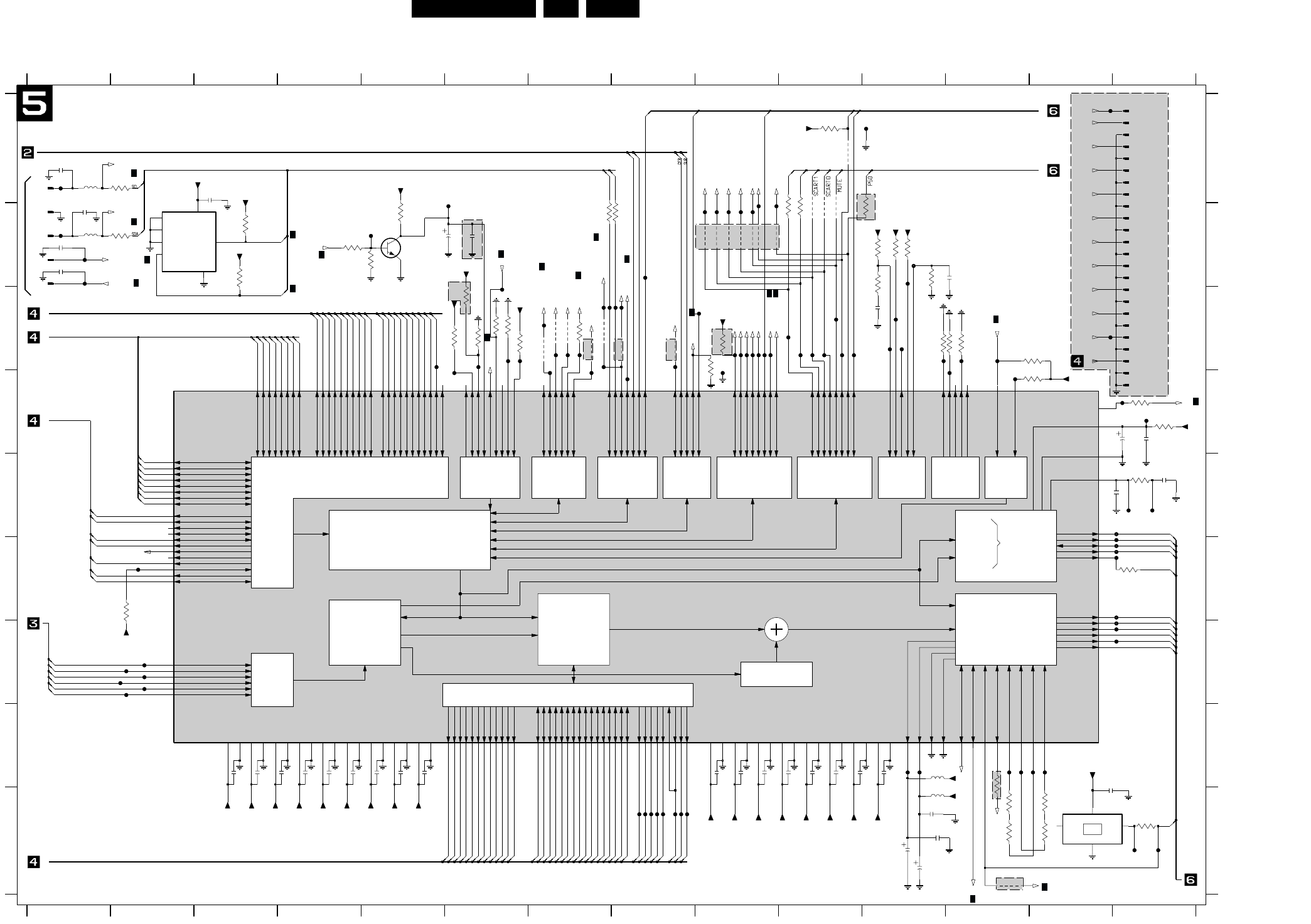
Electrical diagrams and PWB’s 35ASD-1 7.
STI 5505
LPCM AUDIO
IRQPORT 0 I/O PORT 1 I/O
Subpicture
Video
Audio
SDRAM CONTROLLER
SYSTEM USE JTAGPORT 2 I/O PORT 3 I/O PORT 4 I/O
FRONT-END
uP ST20cpu
A/V/Sub
demultiplexer
MPEG
DECODER
Subpicture
decoder
TEST
2
I S
ADDRESS DATA
Interface
MEMORY interface
VIDEO
ENCODER
DECODER
AC3
MPEG1/2
OSC
F568 F2
F569 F14
F573 G14
13
F589 H12
13 14
2526 I11
14
2528 I11
2515 I4
3538 I13
3540 C9
3541 B7
3542 B8
F507 B9
F508 B9
F509 B9
F510 B9
F511 A1
F567 F14
F513 B11
910
3
F590 H13
2
3552 B10
F519 C9
F520 C7
3555 B9
3556 B9
3557 B9
3501 B3
1506-18 C14
2516 I5
2521 I9
F558 D14
F559 E14
F560 E14
F562 E14
F564 F14
BASIC ENGINE INTERFACE Bus
F597 I8
F595 I8
F596 I8
2517 I5
2518 I5
2519 I9
F502 B5
3456
2520 I9
8
F583 G2
3561 B9
F515 B1
2525 I10
1
2529 I11
3537 I12
F504 B9
F505 B9
F506 B9
F592 I8
F593 I8
F594 I8
3511 C6
3512 C6
3513 A10
3573 I12
3515 C6
3545 D14
3546 C7
3547 B6
3548 A10
F512 B1
3550 B10
2522 I10
3502 B5
3516 C6
3517 C13
3519 C9
3520 C11
2506 D14
A
3551 B10
3503 B11
3506 B4
I2C Bus
3504 B11
2527 H13
3505 B11
F516 B1
F517 B11
F518 B6
F503 A6
F556 D12
F557 D12
2513 I4
5503 A1
5504 B1
2512 I4
1506-8 A14
F566 F14
3563 C7
3562 C7
SYSTEM ADDRESS Bus
F514 B8
F578 G2
F579 G2
3549 B10
3523 D13
2509 E13
2510 I3
3564 C7
F531 C10
F574 G14
F576 G14
F521 C10
2524 I10
2530 I11
2531 I11
2532 B1
2533 A1
789
1506-16 C14
1506-17 C14
3509 B11
3536 I14
7504 I13
F546 C9
F547 C9
F548 C9
1506-3 A14
1506-4 A14
1506-14 B14
1506-13 B14
1506-7 A14
H
1506-9 B14
2523 I10
3534 I12
3535 I13
F598 I8
C
1506-1 A14
2507 D14
2508 E14
3507 B5
3553 B11
3554 B10
2534 B1
2535 B1
3500 B3
10 11 12
F539 C6
5501 H11
2514 I4
I
2500 A3
2502 B5
2503 B6
2504 C11
2511 I3
7505 A2
F050 I14
F051 I14
F052 C7
F053 C7
3521 C12
F580 G2
G
E
F
H
F581 G2
F532 C10
F533 C10
F534 C10
F522 C11
F523 C13
3558 B9
3559 B9
3560 B9
B
3508 B11
1506-15 B14
F540 C6
TO/FROM DISPLAY
7501 B5
F588 H12
7
F582 G2
F586 H11
F587 H13
F549 C9
F552 C7
F054 C12
F055 D14
F056 F14
3524 D14
3525 E14
1506-12 B14
D
E
1506-23 D14
B
F524 C10
1506-11 B14
1506-10 B14
1506-2 A14
3565 C8
3566 C7
3567 C7
3568 C8
3569 I12
3570 F14
3571 A2
3572 B2
1506-6 A14
G
I
1506-24 D14
C
D
1506-5 A14
SDRAM Interface
F541 C12
F542 C9
F543 C7
F544 C9
F545 C9
F553 C8
F554 D8
3522 C12
F555 D6
F058 C7
F059 C8
F060 C8
F500 A13
1506-19 C14
SYSTEM DATA Bus
1
F535 C5
1501-2 B1
1501-3 B1
1501-4 B1
1501-5 B1
F
F501 A11
2
F536 C6
F537 C11
F538 C6
F529 D7
F530 C10
HSYNC
5502 I11
F585 H11
11 12
7503 D2
F528 C11
1506-21 C14
1506-22 C14
3514 C6
3526 F2
456
F599 I8
RAM/ROM Interface
F525 C11
F526 C7
F527 C7
1506-20 C14
VDD_STI
OPTION
OPTION
OPTION
OPTION
OPTION
OPTION
OPTION
OPTION
OPTION
OPTION
OPTION
2505 B11
A
1501-1 A1
F521
F531
F553
F599
+5Vstby
F554
5504
F573
VDD_STI
8
68R
3571
1501-1
F528
1506-8
3572
3547
3K3
3562
68R
3534
10K
1506-20
20
VDD_STI
F594
5503
3570
100R
F503
VDD_STI
3566
3557
100R3551
F592
VDD_STI
F512
F514
VDD_STI
3569
F524
F544
VDD_STI
3541 47R
VDD_STI
3520
10K
1506-7
7
F504
3542 47R
1506-12
12
4K7
3507
100n
2511
3546
100R
3508
68R
F060
3501
3559
F576
3K3
F556
F527
100R3550
F587
100n
2525
100n
2518
F579
F533
F559
100n
2503
F522
1506-24
24
F506
VDD_STI
F518
F596
F589
F566
3K3
3500
3K3
3517
2u2
5501
3555
3540
4K7
VDD_STI
F529
F523
21
3K3
3512
2512
100n
1506-21
2507
F546
F595
100n
3563
F558
100n
2515
2520
VDD_STI
2505
22n
100n
F542
+5VOSC
F540
VDD_STI
VDD_STI
VDD_STI
F569
100n
2528
F578
F505
3549
F501
3565
47p
F562
2532
F557
F574
VDD_STI
3552
3553
F500
F581
F530
100R
F513
VDD_STI
100R
1506-14
14
3536
F548
3554
2535
1n
F585
F532
1501-4
F583
1506-22
22
1
VDD_STI
1506-1
F580
F536
10K
100n
2514
3505
F567
100n
2521
10K3504
F535
F564
VDD_STI
10K
3513
3561
100n
2513
11
F586
330p
1506-23
23
1506-11
2509
3558
3524
100R
F516
F515
3522
10K
F560
15
2519
100n
3
F059
1506-15
F520
1506-3
VDD_STI
3556
330R
3537
1n
2534
10K
VDD_STI
VDD9
110
VDDA1
53
VDDA2
60
VDDA_PCM 48
VREF_PCM 49
VSSA1
54
VSSA2
61
VSSA_PCM 50
V_REF_DAC_RGB
58
V_REF_DAC_YCC
65
WE0n
121
WE1n
122
Y_OUT
62
3509
VDD10119
VDD11130
VDD12139
VDD13149
VDD14159
VDD15171
VDD16184
VDD17208
VDD218
VDD334
VDD467
VDD575
VDD686
VDD7
95
VDD8102
SDCS0n84
SDCS1n85
SDRASn88
SDWEn
90
SPDIF_OUT
47
TCK 188
TDI 186
TDO 189
TEST1 30
TEST2 31
32
TEST3
TEST4 33
TEST5 41
TMS 187
TRSTn 190
VDD1
1
PIO-4|3 194
PIO-4|4 195
PIO-4|5 196
PIO-4|6 197
PIO-4|7 14
PIXCLK_27MHz
118
PPC_CLK 137
PPCn_MODE 138
RAS0n_OR_CE4n
127
RAS1n_OR_HOLDREQ
128
136
READY
RSTn 29
R_OUT
57
133
R|W_|DMAACK
SCLK
43
SDCASn89
3
PIO-2|3 5
PIO-2|4 6
PIO-2|5 7
PIO-2|7 8
PIO-3|0 201
PIO-3|1 202
PIO-3|2 203
PIO-3|3 204
PIO-3|4 205
PIO-3|5 206
PIO-3|6 207
2
PIO-3|7
PIO-4|0 191
PIO-4|1 192
PIO-4|2 193
PCM-OUT1
21
PCM-OUT2|PIO-0|6
PCM_CLK
45
PCM_OUTO
44
PIO-0|0 15
PIO-0|3 16
PIO-0|4 17
PIO-0|5 20
PIO-0|7 22
PIO-1|0 9
PIO-1|2 10
PIO-1|3 198
199
PIO-1|4
PIO-1|5 11
PIO-1|6 12
PIO-1|7 13
PIO-2|0
96
103 GND8
GND9
111
G_OUT
56
HSYNCn
51
IRQ0 23
IRQ1 25
I_REF_DAC_RGB
59
I_REF_DAC_YCC
66
LRCLK
46
MEMCLKIN104
MEMCLKOUT76
ODD_OR_EVEN
52
OEn
123
OSD_ACTIVE
117
24
DQMU105
GND14
GND10
120
GND11131
GND12140
GND13150
GND14160
GND15172
GND16
185
GND17200
GND2
19
GND335
GND468
GND577
GND687
GND7
DQ1
93
DQ10
108
DQ11
109
DQ12
112
DQ13
113
DQ14
114
DQ15
115
DQ2
94
DQ3
97
DQ4
98
DQ5
99
DQ6
100
DQ7
101
DQ8
106
DQ9
107
DQML91
DATA11 154
DATA12 155
DATA13 156
DATA14 157
DATA15 158
DATA2
143
DATA3
144
DATA4
145
DATA5
146
DATA6
147
DATA7
148
DATA8 151
DATA9 152
DMAXFER 134
DQ0
92
B_FLAG
38
B_OUT
55
B_SYNC
39
B_V4
42
B_WCLK
40
CAS0n_OR_HOLDACK
129
CAS1n_OR_DMAREQn
132
CE1n
124
CE2n
125
CE3n
126
CSn
135
CVBS_OUT
64
C_OUT
63
DATA0
141
DATA1
142
DATA10 153
ADR2 162
ADR20 182
ADR21 183
ADR3 163
ADR4 164
ADR5 165
ADR6 166
ADR7 167
ADR8 168
ADR9 169
AUXCLK 116
BRM0_OR_OSLINK_SEL 26
BRM1_OR_BOOTFROMROM 27
BRM2 28
B_BCLK
37
B_DATA
36
AD5
70
AD6
71
AD7
72
AD8
73
AD9
74
ADR1 161
ADR10 170
ADR11 173
ADR12 174
ADR13 175
ADR14 176
ADR15 177
ADR16 178
ADR17 179
ADR18 180
ADR19 181
7503
STI5505
AD0
78
AD1
79
AD10
82
AD11
83
AD2
80
AD3
81
AD4
69
16
F582
2531
4u7
1506-16
1506-17
17
F538
100n
2523
2526
100n
3515
10K
F051
F056
F058
+5Vstby
3538
680R
1506-4
4
1506-10
10
VDD_STI
100n
2510
VDD_STI
1506-19
19
F552
F053
5
3564
VDD_STI
1506-6
6
1506-5
VDD_STI
F517
F541
3K3
3523
F593
F526
F525
F549
3516
F545
1
E0
2
E1
3
E2
6
SCL
5
SDA
8
VCC
4
VSS
7
WC_
10K
M24C32
7505
F054
1501-5
F050
1506-9
9
TS
1
VDD
4
1506-2
2
VDD_STI
7504
FXO-31FT
GND
2
OUT
3
F509
F507
F052
100n
2527
47p
2533
F590
F543
3560
F588
F598
3567
VDD_STI
10K
3519
100n
2516
3548
3502
22K
3n3
2508
F547
220R
F055
3514
10K
3545
3568
3526
10K
3506
10K
2502
4u7
2530
4u7
2522
100n
2500
100n
2u2
VDD_STI
+5Vstby
1506-13
13
5502
2517
100n
2504
100p
VDD_STI
F539
18
1501-2
3511
3K3
VDD_STI
1506-18
F555
1501-3
100n
3521
10K
3535
15K
2524
7501
BC847B
F534
10K
3525
VDD_STI
F502
F597
F537
F511
2506
10u
3503
10K
F510
100R3573
F519
F568
F508
100n
2529
VDD_STI
kar_by_pass
RESET_I2C
SERVICE
SPDIF_OUT
SCL_EXE
SDA_EXE
OSD_ACTIVE
SEL_ACLK2
YC2
YC1
YC0
IRQ_I2C
27M_CLKOUT
RESETN
TCK
PCMout1
PCMout2
SDA
P50
STB_CONT
PCM_CLK
CE1
centre_on
27M_CLK1
TXD_SER
{SCLKo,PCM_OUTO,PCM_CLK,LRCLKo,SPDIF_OUT,R_OUT,G_OUT,B_OUT,C_OUT,CVBS_OUT,Y_OUT,27M_CLK}
WAIT
AUXCLK
B_SYNC
B_V4
B_BCLK
B_FLAG
YC5
YC4
YC3
HSYNC
FLASH_OEN
OSLINKIN
YC0
YC1
YC2
YC3
YC4
YC5
YC6
YC7
OSD_ACTIVE
VSYNC
VSYNC
HSYNC
OSLINKOUT
CPUreset
CPUanalyse
ErrorOUT
FLASH_OEN
YC7
centre_on
kar_by_pass
MUTE
SERVICE
RXD_SER
YC6
AD9
AD8
AD7
AD6
AD5
AD4
AD3
AD2
AD1
AD0
SCL
SDA
CTS_SER
RTS_SER
B_DATA
B_WCLK
DQML
WEN
RASN
CASN
CSN2
CSN1
DQ15
DQ14
DQ13
DQ12
DQ11
DQ10
DQ9
DQ8
DQ7
DQ6
DQ5
DQ4
DQ3
DQ2
DQ1
DQ0
AD11
AD10
A4
A3
A2
A1
D8
D9
D10
D11
D12
D13
D14
D15
TDO
LRCLKo
PCM_OUTO
SCLKo
G_OUT
B_OUT
DQMU
RSTN
RAS0ND
RAS1ND
RWN
A20
A19
A18
A17
A16
A15
A14
A13
A12
A11
A10
A9
A8
A7
A6
A5
OS_BOOT
CAS0ND
CAS1ND
CE_ROMN
D0
D1
D2
D3
D4
D5
D6
D7
CLK
OEND
SCL
SEL_ACLK1 TXD_BE
RXD_BE
27M_CLK
27M_CLK
27M_CLK
STB_CONT
CVBS_OUT
C_OUT
Y_OUT
R_OUT
TMS
TDI
TRSTN
3104 123 4268.4
PB 4268 ASD1
MONO-BOARD
4
4
4
4
6
6
2
4
4
4
4
6
6
6
6
6
6
6
6
4
CL06532065_042.eps
180500

36ASD-1 7.
Electrical diagrams and PWB’s
Service interface and Back-end
OSCILL.
CRYSTAL
BUFFER/
CLOCK
+2
BUFFER
OUTPUT
OUTPUT
BUFFER
OUTPUT
BUFFER
BUFFER
OUTPUT
BUFFER
OUTPUT
SYNTHESIS
CLOCK
CONTROL CICUITRY
AND
CLOCK SYNTHESIS
CONTROL CICUITRY
CLOCK SYNTHESIS AND
1603-2 G13
5602 F10
5603 F1
3619 D9
F660 I9
F661 I10
F663 I9
3681 H8
3682 H8
7600-D B12
7600-C A12
3684 I8
3685 I8
3686 E2
3617 D12
3618 D8
1604 G13
1605 E1
1606 E1
5610 D1
6600 C9
7600-A A11
TO AUDIO / VIDEO MUX. BOARD
F644 E11
F643 F10
F630 D12
F631 B3
1603-3 F13
1607 E1
1608 E1
2600 A12
1603-7 D13
1603-8 C13
1603-9 C13
F622 C10
F623 D2
F624 C10
F625 D13
3624 E11
3623 E11
FROM SUPPLY
5608 I9
F618 C2
5607 I9
F619 C11
F620 C13
F621 C6
5604 F10
F629 D10
3688 E3
3689 F3
3690 E4
F628 E6
5600 A13
5601 E5
D
2604 C3
2603 B2
1603-19 E13
7616 G1
1603-20 E13
1603-21 F13
F659 H13
7621 E3
F600 A13
3663 G11
3620 A13
3621 B13
3622 C9
3677 F8
3678 G6
3679 G8
3680 G8
2605 C8
F639 E8
F638 E12
2601 A13
2602 B13
2644 F13
2645 F13
3687 E2
3611 B13
3612 B6
3613 B6
3691 G1
3615 C11
3616 D12
3608 B11
3609 C12
3610 A13
1603-22 D13
I
1603-4 D13
3614 C6
1603-6 G13
1600 B1
E
F
7600-B B11
F626 D10
F627 D2
F616 B13
F617 B7
F615 B2
5609 A2
3626 F11
3627 B7
3628 C7
3629 C10
F652 G10
F653 G11
F640 E11
5605 G10
5606 H9
12 13
A
B
C
F613 B12
F614 B2
7614 G10
7615 H10
2607 D2
F651 G9
7618 I10
7620 E2
2611 D1
2614 F9
TO AUDIO/VIDEO MUX. BOARD
F632 F1
1603-5 F13
1602-1 A13
1602-2 A13
1603-10 C13
F664 I10
2606 C9
F649 F11
1603-13 D13
1603-14 E13
1603-15 E13
1603-16 E13
1603-17 D13
10
2646 H4
3605 D5
3606 C10
3607 B12
BLM31
3683 I8
3630 C8
4
F665 I13
F666 I11
H
3631 F9
G
H
I
3636 C13
3637 C12
BLM31
A
B
C
D
E
F
3625 E11
F671 E2
F672 E2
F673 E3
F674 E3
TO/FROM PC INTERFACE
1603-18 E13
F637 E12
F641 E11
F601 A13
F602 A13
F603 A12
F604 A3
F647 F9
F648 F10
1602-5 B13
1602-6 B13
1602-7 A13
1603-1 E13
F645 I3
2608 B3
2609 C2
2610 F6
7604 B7
7605 B3
7607 B6
3664 G10
3665 E11
3667 E11
3669 G1
3670 G1
F605 A2
F606 A12
7
2623 H10
9101112
F654 H9
SERIAL PC INTERFACE
2615 F10
119
123
2640 F12
2641 F12
2642 F12
2643 F12
F609 B6
3632 F10
3633 G9
3635 B13
F610 B7
F611 B13
F612 B12
F657 H11
F658 H13
678
F669 C11
F670 C2
2622 H9
3658 I10
2624 I9
2625 I9
2626 I9
2627 I9
13
F636 C2
F635 E12
8
1603-11 C13
1603-12 D13
1602-3 A13
1602-4 B13
3673 G3
3674 D11
3675 I4
3676 E5
7612 F11
7613 F11
3655 I10
3656 I10
3657 H10
7617 I10
3659 I10
3642 B6
2616 G9
2617 G10
2618 F2
2619 F2
56
3660 H11
3661 G10
3662 G11
2632 C9
2633 C9
2634 C2
2635 C3
F655 H10
F656 H13
F633 E12
F634 C3
G
2638 D3
2639 D4
2636 C4
2637 D2
F607 A13
F608 B3
OPTION
OPTION
OPTION
OPTION
OPTION
OPTION
7609 C10
3647 G9
3648 H9
3651 I9
3654 I9
2620 G9
2621 G10
1 2345
3671 G1
3672 C3
F646 F11
7600-E A9
7600-F A8
7608 C11
7610 D10
7611 F5
2641
1603-11
11
OPTION
OPTION
OPTION
47R
3672
22p
1K
-Vvid
12 14
7
-Vvid
3659
F606
74HCT14D
7600-F
13
1603-21
21
F626
F635
2627
47p
5600
F649
1n5
2601
22p
2645
+5VOSC
-8Vstby
2643
22p
7
PS015
PS116
PS21
VDD1
4
VDD2
13
X13
X22
BC847B
7613
7616
MK2742
13_5M 10
27M 9
3_68M 14
ACLK
6
AS08
AS112
GND1
5
GND2
11
PCLK
2606
100u
+5V
-Vvid
1602-7
PH-S7
3658
1K
F641
1603-19
19
+5V
5605
15u
+6Vstby
+5V
+5V
5603
3681
100n
2603
F654
1K
3660
1603-22
22
22n
2600
F609
430R
2623
47p
100n
3657
100n
2636
47p
2620
2618
1603-1
1
7615
F625
3619
22K
BC847B
+5V
VDD_STI
2602
+5V
22K
3618
+5V
1n5
1603-17
17
+5V
+5VOSC
2634
100n
1602-5
PH-S5
3611
10K
100u
2632
100K
3609
+5V
F644
1606
3637
3K3
F651
1603-3
3
F621
F669
3628
470R
VDD_STI
7609
BC857B
F652
F623
3671
22K
3617
10K
47K
3606
F631
PH-S
1602-6
6
100n
2610
F666
F613
1602-2
PH-S2
-8Vstby
6K8
3635
F670
F632
F637
5608
15u
56 14
7
3622
100R
7600-C
74HCT14D
3651
430R
3678
+5V
BC847B
7604
3610
10K
-Vvid
3684
+3V3
47p
2624
+5V
3683
3689
22K
+5V
1K
3662
22K
3687
2621
+5Vstby
7600-B
74HCT14D
34
14
7
47p
100R
3623
F603
3663
1K
1603-20
20
+5V
7611
74HCT1G125
2
1
5
3
4
F629
PH-S
1602-4
4
1607
3685
F601
13
14
15
16
2
3
4
5
6
7
8
9
1604
1
10
11
12
100MHZ
5610
-Vvid
F630
LD1117
7605
1
GND
3IN 2
OUT
7
+12Vstby
+12Vstby
430R
3656
74HCT14D
7600-D
98 14
F658
100K
3607
1603-13
13
7600-A
74HCT14D
12
14
7
100R
3625 F638
VDD_STI
7
100u
2611
3682
1603-7
3679
F633
15u
5602
F605
F611
F607
10K
3615
F653
3620
100R
3688
4K7
F671
430R
+5V
3673
3655
5606
15u
+5V
430R
3633
3647
430R
F622
+5VOSC
+3V3
F610
430R
F664
F672
3661
1605
1603-6
6
1608
47u
2609
+3V3S
430R
3664
F647
2614
47p
15u
5607
10K
3642
F619
2633
100u
F617
2604
100u
F624
F614
12
2
3
4
5
6
7
8
9
1600
1
10
11
3686
22K
2616
-8Vstby
47p
1PS76SB10
6600
47p
10K
3613
2622
1603-16
16
F615
3614
10K
3680
1603-10
10
F646
F618
F648
2617
47p
STB_CONT
+5V
2639
100n
VDD_STI
3691
10u
2608
3670
+5Vstby
-Vvid
F663
F616
220R
F661
F645
3630
F602
F674
100n
2638
-8Vstby
2626
47p
2625
47p
-8Vstby
+6Vstby
3632
430R
15u
5604
BC847B
7612
F628
BC847B
7607
1603-9
9
3669
100n
2635
7621
BC817-25
-8Vstby
3621
100R
2644
22p
3676
F657
4K7
3629
430R
3648
100MHZ
5601
F660
F620
F656
+5V
2605
22n
BC847B
7617
F636
F639
1603-2
2
BC847B
7618
+5VOSC
8
3612
10K
1603-8
6K8
BC857B
7608
+5V
3636
BC847B
+3V3
+5V
3616
10K
7610
F612
1603-15
15
2615
47p
F665
F655
7614
BC847B
3674
100MHZ
5609
F608
330R
3667
2619
100n
3665
22R
7620
BC857B
22p
2640
3690
F634
+5V
PH-S
1602-1
1
1603-4
4
1603-14
14
1603-12
12
F640
3
F604
+5VOSC
1602-3
PH-S
5
430R
3654
2642
22p
1603-5
18
2637
100n
1603-18
-Vvid
3605
2607
100u
+5V
74HCT14D
7600-E
1110 14
7
+5V
F627
+5Vstby
+12Vstby
F673
-8Vstby
3624
100R
430R
3631
470R
3627
3608
100K
3677
1K
3626
F643
F600
22p
2646
F659
3675
SCLK
LRCLK
CFLG
B_FLAG
MEAS1
P50
SEL_ACLK2
SEL_ACLK1
CVBS_OUT
C_OUT
{SCLKo,PCM_OUTO,PCM_CLK,LRCLKo,SPDIF_OUT,R_OUT,G_OUT,B_OUT,C_OUT,CVBS_OUT,Y_OUT,27M_CLK}
SCLKo
PCM_OUTO
PCM_CLK
LRCLKo
SPDIF_OUT
CVBS
R_OUT
G_OUT
B_OUT
RTS_SER
HSYNC
Y_OUT
R_VID
PCMout2
PCMout1
SCL
SDA
Y_VID
C_VID
B_VID
G_VID
RXD_SER
CTS_SER
SERVICE
TXD_SER
SCART0
SCART1
0_6_12V
0_6_12V
MUTE
MUTE_AV
3104 123 4268.4
PB 4268 ASD1
MONO-BOARD
5
5
5
5
5
66
5
CL06532065_043.eps
180500
Electrical diagrams and PWB’s 37ASD-1 7.
Top view
CL06532065_044.eps
230500
SUPPLY
AV1
AV2
SERVICE
I2C
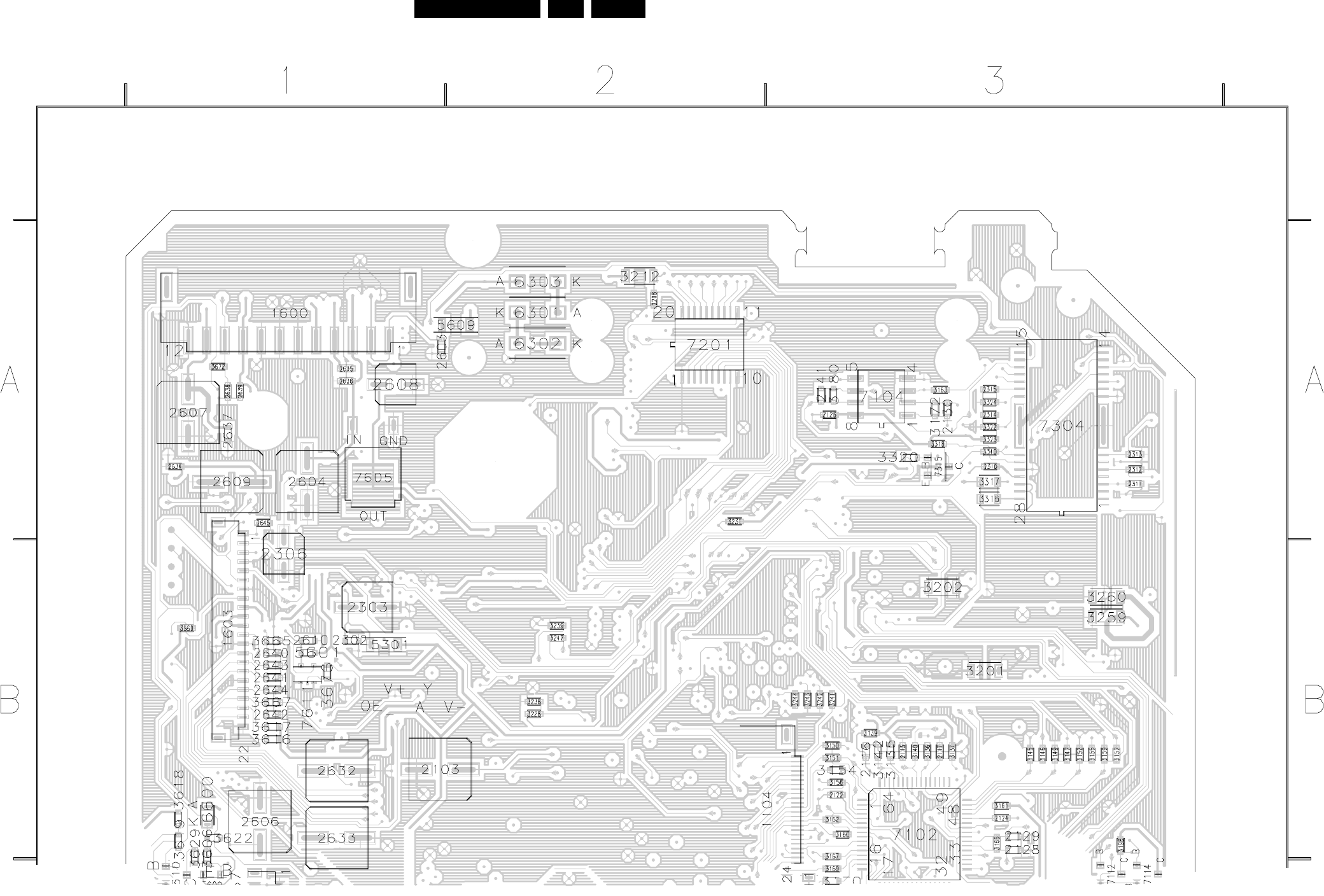
38ASD-1 7.
Electrical diagrams and PWB’s
Detailed Top view 1
CL06532065_045.eps
180500
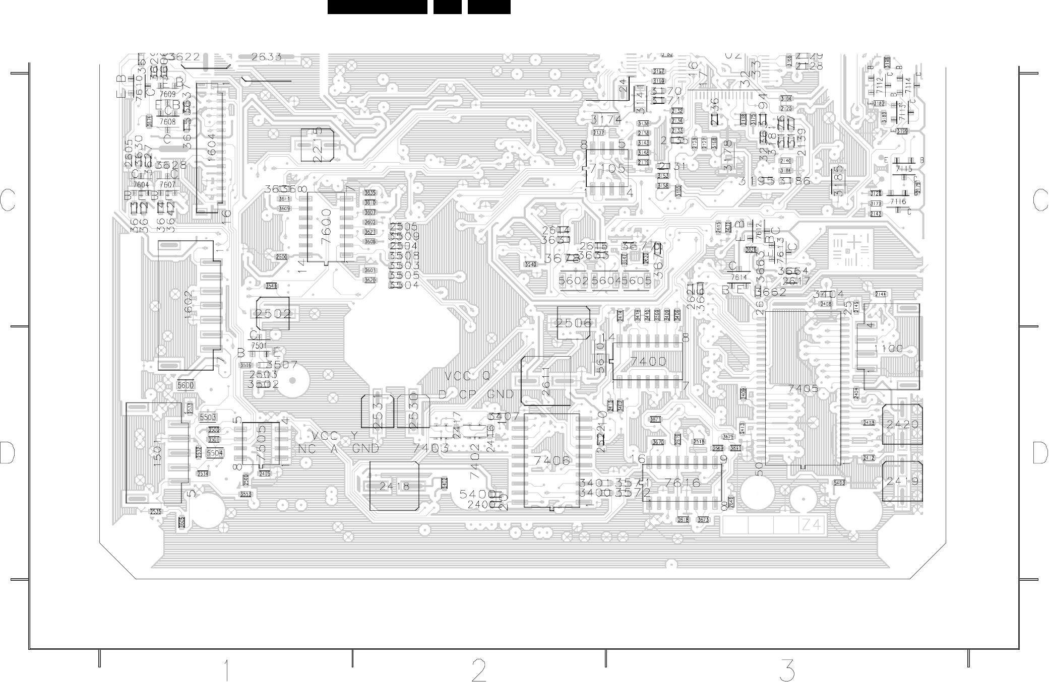
Electrical diagrams and PWB’s 39ASD-1 7.
Detailed Top view 2
CL06532065_046.eps
180500
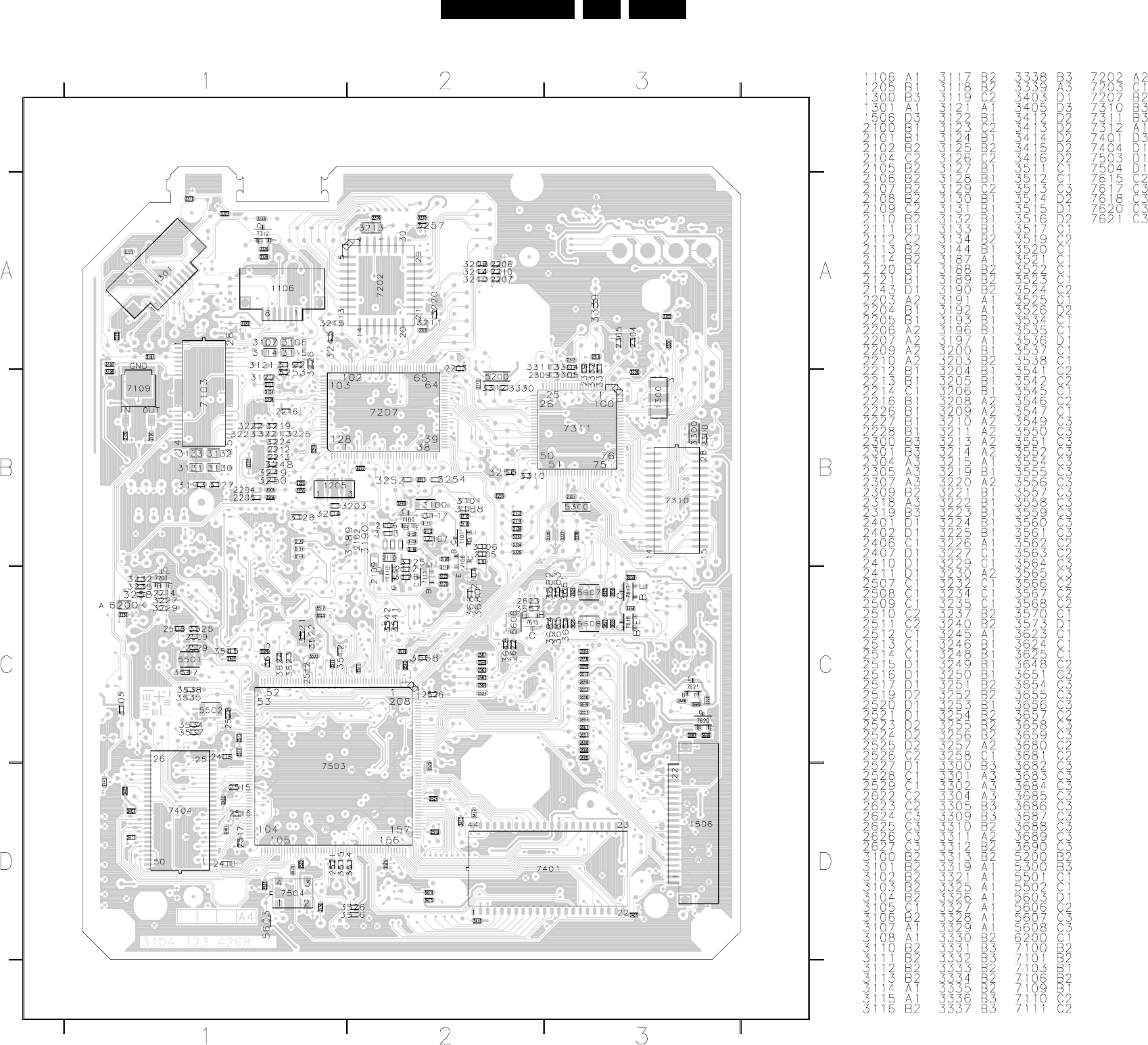
40ASD-1 7.
Electrical diagrams and PWB’s
Bottom view
CL06532065_047.eps
180500
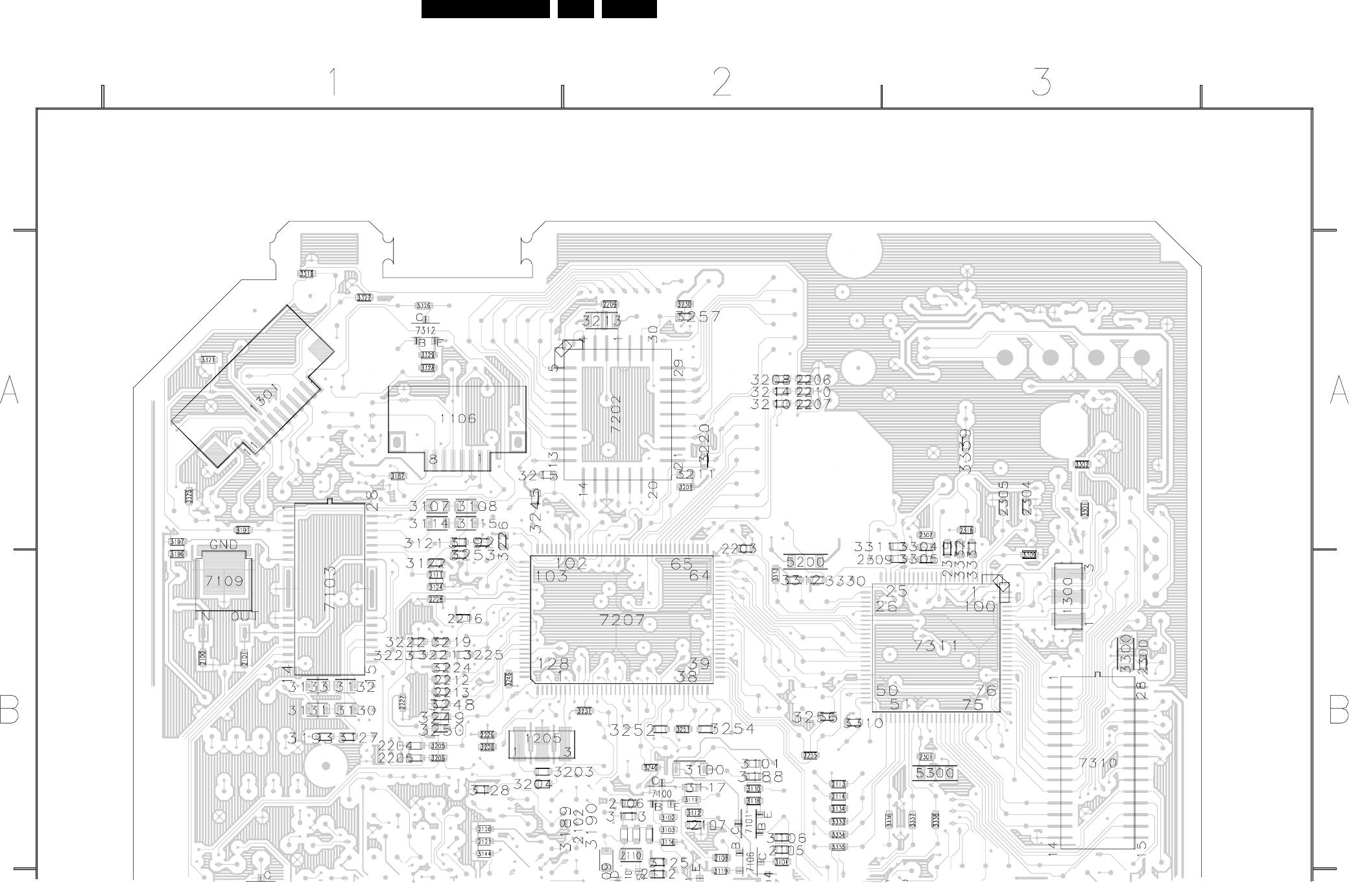
Electrical diagrams and PWB’s 41ASD-1 7.
Detailed Bottom view 1
CL06532065_048.eps
180500
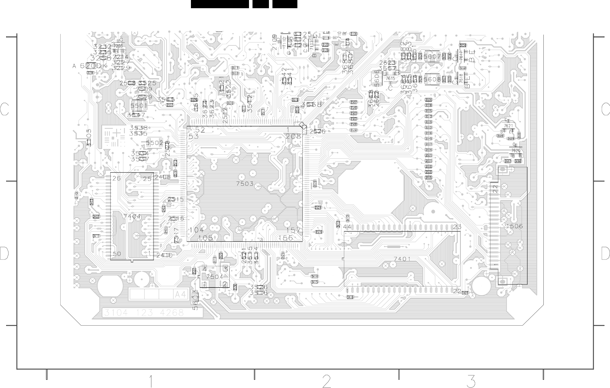
42ASD-1 7.
Electrical diagrams and PWB’s
Detailed Bottom view 2
CL06532065_049.eps
180500
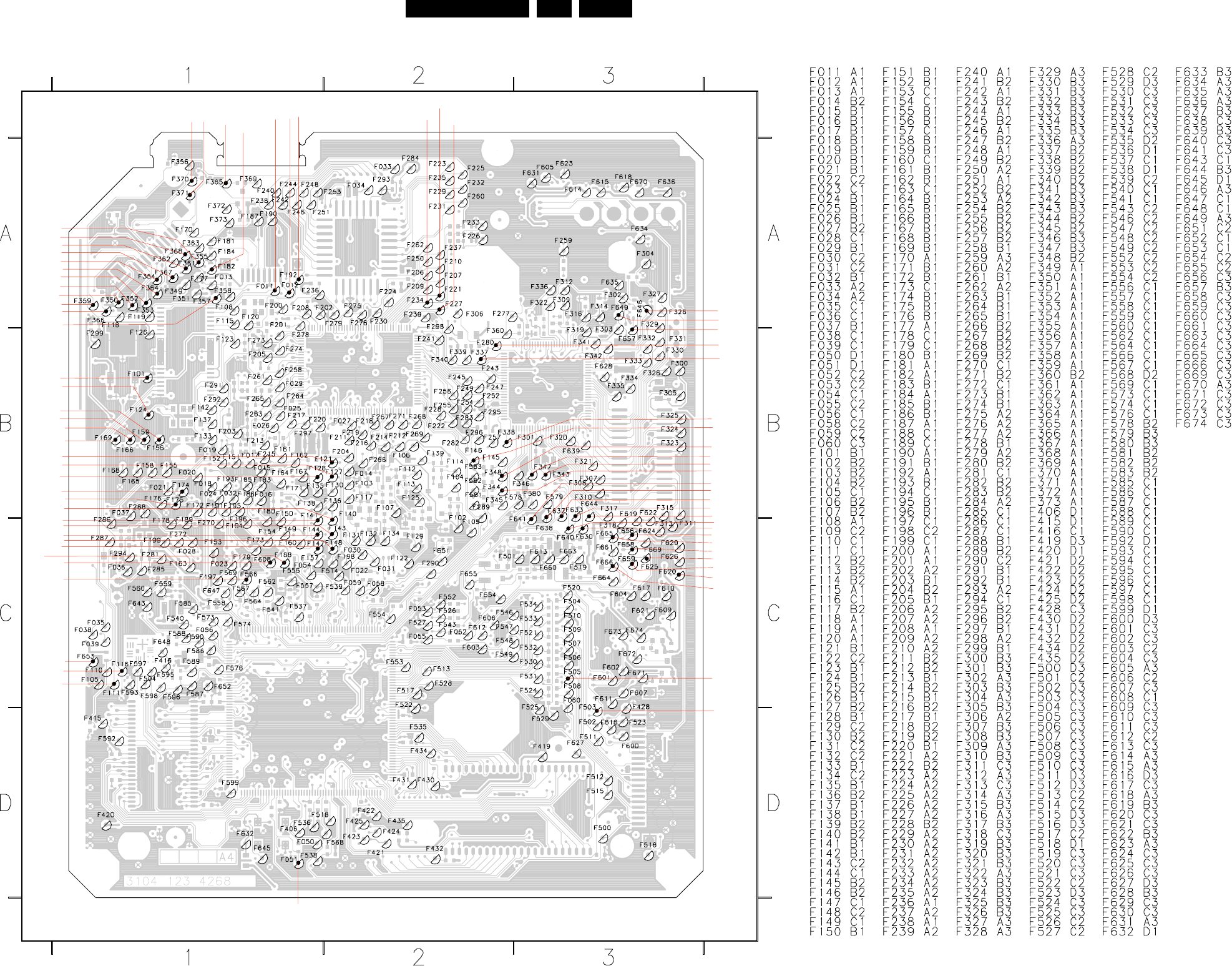
Electrical diagrams and PWB’s 43ASD-1 7.
Testpoint overview
VH
H3-
Stby-out
T2
MOTO1
H3+
H1+
H2+
A1
A2
A3
H1-
H2-
Stby
9V
FOC-
O1
O2
O4
O3
RAD+
FOC+
RAD-
S2
S1
A
B
C
D
F
E
2.5V 3V3
PCM_CLK
B_VID
VO2-
VO2+
27M_CLK
R-VID
G-VID
CVBS
T1
CL1
STOPCLK
RFO
B_V4
B_BCLK
B_WCLK
B_SYNC
LRCLK
PCMOUT0
SCLK
DEEMPH1
SPDIF
PCM_CLK
DEEMPH0
HSYNC
C_VID
PCMOUT2
MUTE
PCMOUT1
SCART
Y_VID
STB_CONT
RSTN
SL+ FO
SL
RA
Sinph
SL- Cosph
T3
CL06532065_050.eps
180500

44ASD-1 7.
Electrical diagrams and PWB’s
Personal notes: Personal notes:
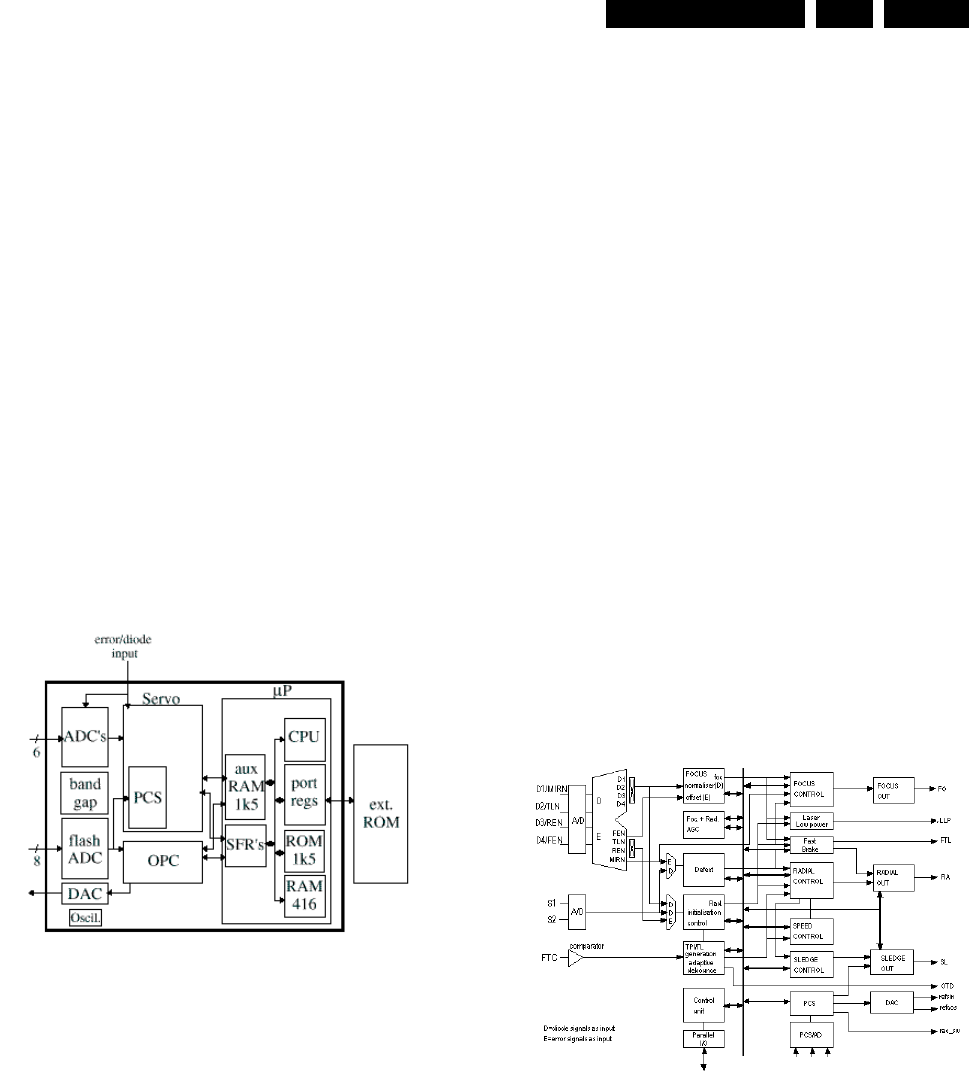
Alignments GB 45ASD-1 8.
8. Alignments
No alignments available
9. IC Descriptions.
9.1 SAA7399 (MACE2) General.
Mace2 is a name used for the successor of the ACE1 IC. The
term MACE (mini-ACE) is used because MACE2 does not
have a decoder on board. Application area's: Mainly CD-
R(W) and prototyping of DVD(-ROM) or high speed CD-
ROM.
Functions implemented on-board of MACE2:
A further improved digital servo module. Derived from the
ACE1 servo module, but with improvements (make the input
switchable between diode signal and error signal processing,
improved brake).
The 80C51 micro-controller with external ROM.
The OPC. Optimum Power calibration, used for CDR.
The PCS. Position Control Sledge. A way to speed up sledge
movement using hall sensors.
Figure 9-1 Overall block diagram MACE2.
9.2 Features
•Focus and Radial servo loop.
•Built-in access procedure.
•Selectable servo error or servo diode inputs.
•Focus noise performance equivalent to DSICS
•Automatic closed loop gain control available for focus
and radial loops
•High speed track crossing velocity measurement > 350
kHz.
•Fast Radial Brake circuitry.
•Sledge motor servo loop, with pulsed sledge support and
PCS
•Incorporated micro-controller equivalent to 80C51
--> 66MHz.
•Programmable wait state controller.
•Two embedded RAM's of 416 bytes and 1.5 kB res.
•Optimum Power Calibration Hardware support up to
write at N=8.
•Debug facilities.
•Memory mapped interface to sub-modules.
•Programmable clock multiplier.
•8 Multipurpose I/O lines.
•5 external interrupt lines.
•External Flash ROM support.
•Sledge stepper motor support.
9.3 The Digital Servo block.
In a CD system, there are some 12 control loops active.
About six of them are needed to adjust the servo error
signals, that is once per disc rotation offsets, signal
amplitudes and loop gains (AGC's) are adjusted to enlarge
system robustness and to avoid expensive potentiometer
adjustments in production. The other six loops determine the
laser spot position on the disc in the radial, axial (focus) and
tangential directions. The servo in MACE2 takes care of
these controls.
The servo inside Mace2 also has to take care that the spot
accesses a required position as fast as possible. This access
system consists of two parts, namely the actuator and the
sled, which are within a certain range, mechanically and
electrically independent. So during an access the servo has
to control as well the actuator as the sled.
9.4 Functional description servo
Figure 9-2 Mace2 servo block diagram.
The following functions can be distinguished:
–A to D conversion: a direct AD-conversion of the diode/
error currents.
–Pulse density D to A conversion: Noise shaper output
stages.
–Control unit: Provides mainly the communication and on/
off functions.
–Focus normaliser: A partial division of focus and sum
signal. Special saturating provisions are included when
dividing through very small numbers.
–Initialisation control: Includes the radial normaliser,
automatic radial offset compensation and level
initialisation for the Track Position Indicator (TPI) for both
diode and error input signals.
–TPI/TL generation and adaptive debounce: Generates
Track loss (TL) which is protected against disc defects.
The TL is made out of the unprotected TPI signal. The
debouncer (with improved debounce times) minimises
the disturbing effect of HF on the TL and Rp crossovers
for the track count circuitry.

IC Descriptions.
GB 46 ASD-19.
–Defect detector: Holds the focus and/or radial control
signal on disc dropouts.
–Speed control: Used during access. With radial actuator
feed forward.
–Focus control: PID controller with wide range adjustable
characteristics.
–Radial control: PID controller with wide range adjustable
characteristics.
–Sledge control: PID controller with wide range adjustable
characteristics and a pulsed sledge controller.
–Laser Low Power: Switches the laser from write back to
read power whenever the device tends to go off-track.
9.5 Input circuits servo
Five out of six of the MACE2 servo inputs can be switched
between diode current inputs (for audio and data application)
and error signal inputs (for recordable applications).
The analogue signals from the diode pre processor are
converted into a digital representation using A/D converters.
9.6 Focus control.
9.6.1 Focus start-up.
To bring the actuator in focus position a triangular shaped
voltage is applied to the actuator to perform a search
movement. When the lens moves from or to the disc, CA
(central aperture) is monitored to reach a certain
programmable absolute level. When this value is CA level is
reached, the FOK signal becomes true and FEn is passed to
the FEn level detector.
At the moment this FEn level is reached the wait for the focus
mode is entered and the focus control loop is enabled to
detect a sign inversion in the FEn signal.
When this zero crossing in this FEn signal is detected, the
loop is closed to function as PID controlled loop and is
switched to the PID mode.
During focus start-up a dither signal is added to the output
signal of the integrator. It prevents the actuator from hitting its
natural resonance. With this technique quantisation, effects
are compensated for during start-up.
9.6.2 Focus Position Control loop.
The focus control loop contains a digital PID controller that
has 5 parameters available to the user. These coefficients
influence the integrating, proportional and differential action
of this PID and a digital low pass filter following the PID. The
fifth coefficient influences the loop gain.
9.6.3 Dropout detection.
This detector can be influenced by one parameter. The FOK
signal will become false and the integrator of the PID will hold
if the CA signal drops below this programmable absolute CA
level. When the FOK signal becomes false, it is assumed as
caused by a black dot in the first place.
9.6.4 Focus Loss detection and Fast restart.
Whenever FOK is false longer than about 2 ms, it is assumed
that the focus point is lost. A fast restart procedure is initiated
which is capable of restarting the focus loop within 200 to 300
ms depending on the uP-programmed coefficients.
9.6.5 Focus Automatic Gain Control loop.
The loop gain of the focus control loop can be corrected
automatically to eliminate tolerances in the focus loop. This
gain control injects a signal into the loop that is used to
correct the loop gain. Since this decreases the optimal
performance, the gain control should only activated shortly
(for instance when starting a new disc).
9.7 Radial control.
The MACE2 digital controller includes the following radial
servo functions:
9.7.1 Level initialisation:
During start-up an automatic adjustment procedure is
activated to set the values of the radial error gain, offset and
satellite sum/MIRN signal gain for TPI level generation. The
initialisation procedure runs in a radial open loop situation
and is < 200 ms. This start-up time period may coincide with
the last part of the turntable motor start-up time period.
9.7.2 Automatic gain adjustment:
Because of this initialisation the amplitude of the RE signal is
adjusted within _10% around the nominal RE amplitude.
Offset adjustment: The additional offset in RE due to the
limited accuracy of the start-up procedure is less than +/-
50nm.
9.7.3 TPI level generation:
The accuracy of the initialisation procedure is such that the
duty cycle range of TPI becomes 0.4 < duty cycle < 0.6.
Sledge home:
Sledge moves to reference position at the inner side of the
disc with user defined voltage.
Tracking control:
The actuator is controlled using a PID loop filter with user
defined coefficients.
Access:
In Mace2 there are two fundamentally different ways to
perform an access:
Using the PCS
A more detailed description of this access method is given in
an other section.
Using the servo controlled access:
The way it was done in the predecessors of Mace2.This
access procedure is divided into 3 different modes,
depending on the requested jump size:
access type size access speed
Actuator jump decreasing velocity
Sledge jump maximum power to sledge 1
Controlled sl. jump controlled brake power
The access procedure makes use of a track counting
mechanism, a velocity signal based upon the number of
tracks passed within a fixed time interval, a velocity setpoint
calculated from the number of tracks to go and a user
programmable parameter indicating the maximum sledge
performance.
If the number of tracks to jump is too large, then the Sledge
jump mode is activated, else the actuator jump is performed.
The requested jump size together with the required sledge
braking distance at maximum access speed defines the
value of the maximum numbers of tracks.
During the actuator jump mode, velocity control with a PI
controller is used for the actuator. The sledge is then
continuously controlled using the filtered value of the
integrator contents of the actuator. All filter parameters (for
actuator and sledge) are user programmable.

IC Descriptions. GB 47ASD-1 9.
In the sledge jump mode maximum power (user
programmable) is applied to the sledge in the correct
direction, while the actuator becomes idle.
Radial Automatic Gain Control loop:
The loop gain of the radial control loop can be corrected
automatically to eliminate tolerances in the radial loop. This
gain control injects a signal into the loop which is used to
correct the loop gain. Since this decreases the optimal
performance the gain control should only be activated shortly
(for instance when starting a new disc). This gain control
differs from the earlier mentioned level initialisation. This
level initialisation should be done first. The level initialisation
without the gain control reduces tolerances from the front-
end only.
9.8 The radial PID.
Since we are dealing with a big variety of applications and
drives, the servo controllers in MACE2 should be adjustable
within a large frequency range.
In order to read out the track properly -a track consists of
sequential ordered data pit's which hold audio, video or ROM
data - the focus and radial position controls must follow the
moving track within some tenths of a micrometer, despite of
disc imperfections and external disturbances.
For instance, a rotating disc causes, due to track eccentricity,
track unroundness, or disc skew, track movements up to
some millimetres. The control loop reduces this to about one
tenth of a micrometer.
9.9 Initialisation control.
Due to optical, electrical and mechanical tolerances in CD
players, properties of the servo signals such as offset and
gain can vary. In general, without proper signal processing, a
simple PID controller function cannot cope with this relatively
large offset and gain spreads. Therefore, gain and offset
adjustments during manufacture or active control, to
compensate for these signal imperfections, become
inevitable.
Adjustment procedures in the factory are expensive. So,
automatic adjustment procedures have been implemented in
order to avoid most of the potentiometer adjustments. In the
MACE2 servo automatic adjustments are applied to the
radial error signal only.
9.10 The AGC.
The Automatic Gain Control is used in the MACE2 digital
servo to adjust the radial and focus bandwidths to a nominal
value. Injecting a signal in the loop and measuring the phase
of its resulting signal (wobble method) does this.
Principle of the Automatic Gain Control.
The principle of the Automatic Gain Control (AGC) circuit, as
used in MACE2, is drawn in the next figure.
Figure 9-3 Principle of the automatic gain control.
A sine wave signal with a certain frequency is injected in the
control loop at the summation point. The resulting signal is
measured before the injection point. The injected signal is
shaped by H/1+H . This measured signal is multiplied by a
phase shifted version of the injected signal. The result of the
multiplication is low pass filtered and integrated. (The
integrator is started at the nominal gain of the control loop).
The result of the integration is fed to the adjustable loop gain.
This principle, synchronous detection, is also known as
'wobble method'.
9.11 The Fast brake.
The fast brake is an aid to speed up radial capture after a
high-speed jump. It is a separate radial control with a much
higher bandwidth. The radial control output can be switched
between fast brake mode and original radial control mode.
The fast brake helps the radial actuator at the end of a jump
to "stick" to the right track. In fast brake mode, the actuator
starts to follow the track movements. It's a bit like jumping on
a moving train. If you run as fast as the train, you can just step
in. After a radial open loop jump the tracks are moving (as a
result of eccentricity) at a very high speed underneath the
radial actuator. This speed is too high for a normal radial
control loop to do radial capture. When the radial control is
switched over to fast brake mode for a short term, this moving
of the tracks underneath the actuator becomes much slower,
(because the actuator follows the track movement), so when
you switch back to original radial control, it's much easier to
do radial capture.
9.12 The Defect Detector.
Because of the possible earlier mentioned defects
(fingerprints, etc) a defect detection circuit is incorporated
into the MACE2 servo. If a defect is detected, the radial and
focus error signals may be zeroed, resulting in better
playability.
9.12.1 Operation:
The defect detector prevents the light spot from going out of
focus and going off track due to disc dropout excitations. The
defect detector can be switched on and off under software
control and can be applied to the focus control only, or both
to the focus and radial control.
Whenever this circuit detects a defect, it will hold all radial
and focus controls.
The hold signal is generated whenever the reflected light
intensity drops rapidly (< 1:5 ms) down to roughly 75% of the
actual intensity level. In that case the output of the
comparator becomes active and controls the focus and radial
signal switch.
This circuit improves the playability of the application (black
dot performance, etc) and is programmable to optimise it for
specific disc defects. The actions of this circuit can be
monitored on the DEFO pin (active high).
An external defect detection circuit can be added by
removing the connection between DEFO and DEFI (normal
operation) and inserting the external circuitry.
These signals are afflicted with some uncertainties caused
by:
–Disc defects like scratches and fingerprints
–The HF information on the disc, which is considered as
noise by the detector signals.
9.13 Laser Drive On.
The LDON pin is used to switch the laser drive off and on. It
is an open drain output. In case the laser is on, the output has
a high impedance. The pin will be automatically driven if the
focus control loop is switched on.
IC Descriptions.
GB 48 ASD-19.
9.14 Laser Low Power (LLP).
The LLP output can be used by write-able systems to switch
the laser back to read power when the light spot goes off-
track while writing discs. To prevent that the neighbour tracks
are damaged when the spot goes off-track the laser has to be
switched very fast to the safe read power. The laser is not
switched off (like LDON does), so the system can carry on
reading.
The tracking (radial) and focus error signals are used to
disable the laser write power. This is done through the LLPn,
active low Laser Low Power, signal. Note that LLPn is a servo
output, which is inverted before it is output via the LLP pin, so
the LLP pin is active high.
So, if any of the following conditions is true, the laser write
power is disabled by the MACE2 servo.
–Off Track, more than a quarter off a track away from the
correct one
–ORD, radial error signal too large. Larger than the given
setpoint, which should be chosen at a critical write failure
level. An adjustable band pass filter first processes the
radial error signal.
–OFD, focus error signal too large. Larger than the given
setpoint, which should also be chosen with care. An
adjustable band pass filter also first processes the focus
error signal. All settings of the focus and radial part are
independent.
–OTR, prot stat flag which becomes active if ORD
becomes active during an actual laser write ( LWR)
action. This flag is reset only by a status read ( RSTAT)
command. So until then LLPN stays active.
–OFO, prot stat flag that becomes active if OFD becomes
active during an actual laser write action. Same idea as
OTR.
This error detection circuit can be switched off (apart from the
Off Track detection) by raising the setpoint levels to its
maximum value.
9.15 The OPC.
The OPC block in Mace2 is used for the following functions:
•During write actions, it stores Pw samples, which can be
evaluated by the microprocessor.
•During OPC read actions, it stores A1, A2 and CALF
samples, which are used for calculating the asymmetry
and the modulation index.
•The OPC block is used for EFM detection.
•During reading of a disc, it stores A1 and CALF samples,
which can be monitored.
Although the OPC block is used for multiple functions, it got
it's name from the OPC procedure, which is it's main task.
The OPC (Optimum Power Calibration) procedure is used in
CD-R/CD-RW/DVD-RAM applications. It is used to
"calibrate" the laser write power in writable systems.
It reads in 3 analogue signals from an analogue pre-
processor like AEGER-2 (A1, A2, and CALF) and the actual
write power (Pw) from the laser controller and feeds an
analogue output signal Alpha0 back to AEGER-2. A1, A2 and
CALF represent the max, min and average value of the EFM
signal respectively. Alpha0 controls the laser write power. All
analogue signals are converted to an 8 bit digital signal.
Conversion frequency at 16.9MHz base clock is 88kHz (each
channel).
Figure 9-4 Definition of the A1, A2 and CALF signals.
9.16 Definition of terms.
The asymmetry ( and modulation index m of the EFM signal
are calculated from the analogue inputs:
9.17 Rough description of the OPC procedure
Basically the OPC procedure tries to find out the optimum
laser power to be used on a specific disc. The OPC
procedure uses about 15 ATIP frames. These frames are
located in the "PCA" area. This is a special part of the disc
used only for power calibration. The drive first checks
whether there are 15 frames "empty" in the PCA. Next the
OPC is performed in these 15 frames.
The OPC operation consists of two stages: A "write" and a
"read" stage. First 15 ATIP frames are written (during which
the OPC block stores Pw samples), and then the same 15
ATIP frames are read back again, (during which the OPC
block stores A1, A2 and CALF samples). During the write
stage, random EFMis written in a test area located on the
inner side of the disc. During this recording the write power is
increased stepwise from a low to a high power level.
Figure 9-5 Figure 5: OPC write profile.
First during 3 ATIP frames the power is increased in rather
big steps (rough OPC). During this action Pw samples are
stored into memory. During the rough OPC, the OPC makes
7 steps per ATIP frame. This gives 21 samples into the OPC
memory. From these samples, the microprocessor can
calculate what's roughly the best alpha0 setting for this
typical disc.
After 2 frames of calculations, another 10 ATIP frames are
written using smaller steps (fine OPC) around the alpha0
setting, which gave the best result during the rough OPC.
The second stage of the OPC procedure is the "read" phase
A1- A2
A1+A2
m
A1+ A2
A1+CALF

IC Descriptions. GB 49ASD-1 9.
in which the pattern recorded in the previous stage is read
back.
During this read phase the OPC block stores A1, A2 and
CALF samples from exact the same location where during
the OPC write phase the Pw samples where stored. The
samples for A1, A2, CALF and Pw are listed side by side into
memory. After the read back phase the processor calculates
at which setting of alpha0 the least jitter is encountered.
This setting will be used to write the disc with.
9.18 The OPC top level.
The OPC block as a whole has 5 possible modes:
–Recording mode: This can be either OPC writing (writing
EFM test patterns to disc and Alpha0 stepping) or
standard write mode (i.e. alpha0 is constant).
–OPC reading: Reading back OPC test patterns from disc.
–Normal read mode: detects the presence of EFM.
–DVD read mode: used for DVD-RAM experiments.
–EFMD only mode: no data being written to the AUX RAM,
but the EFM detector and the PW monitor still running.
Contents of the QUX RAM remain unchanged.
All actions in the OPC hardware are synchronised to the
ATIP frame sync, which can be either generated internally or
received from the encoder/decoder during writing. The
microprocessor writes data asynchronously to the OPC
hardware. The OPC block synchronises this data to the sync
either internally generated, or obtained from CDR60.
9.19 The Analogue to Digital converter.
The analogue to digital converter of the OPC is shared with
the ADC required by the PCS.
9.20 The digital input filters.
The combined ADC for the OPC and the PCS delivers a
multiplexed stream of 8 bit words. A sequential low-pass filter
filters this multiplexed stream. The 4 analogue multiplexed
input signals from the OPC (A1, A2, CALF and Pw) are
filtered by 4 identical LPF's. (One for each channel). This
filters can be adapted to various speeds by changing the
subsampling factor (i.e. the sample rate of the filter), the cut
off frequency scales with the sample frequency. The sample
frequency of the filter is equivalent to the OPC timebase
frequency, which is the output of the pre-scaler.
9.21 OPC demux.
The OPC demux block demultiplexes the stream supplied by
the LPF. This same block also changes the format of the
digital data from signed (representation inside the filter) to
unsigned (representation in the rest of the OPC). The
demultiplexing process introduces one baseclock delay.
9.22 The sequencer.
The OPC sequencer controls the timing of all the hardware
actions in the OPC hardware. It generates the OPC timebase
and locks it to the ATIP pulse. A programmable pre-scaler
generates the OPC timebase.
Dividing the ADC sample clock by 8 derives the input clock of
this pre-scaler. (= Identical to the sample rate per channel).
The pre-scaler can divide this clock by a number in the range
from 1-16. The division factor can be programmed via the
OPC ctrl register. The OPC timebase is locked to the
selected ATIP source, which can be either an external
ATI P sync or an internally generated sync. (Programmable).
The OPC timebase clock supplies the sample frequency for
the input LPF's, the OPC pre-processor and the EFM
detector.
The sequencer controls the timing of all the hardware actions
in the OPC hardware. The sequencer is started either by an
external ATIP sync or an internally generated sync
(programmable).
All data acquisition and alpha0 settings change synchronised
to this sync signal (rising edge of the ATIP sync). An
exception on this is the switching of the ATIP input itself,
which is immediately changed whenever the bit in the OPC
ctrl register is changed. When this was latched on the ATIP
source itself, it would create a deadlock when there was no
ATIPin from CDR-60.
9.23 The Pw monitor
The Pw monitor is used during the "OPC write" and normal
write mode. The comparator compares the incoming Pw with
two programmable thresholds PW MAX and PW MIN. Both
these thresholds can be programmed via the OPC PW
register, which contains 4 bits for each threshold.
Internally both 4-bit thresholds PW MAX and PW MIN are
extended to 8 bit values. The compare function performs an
unsigned compare.
The first threshold is used to detect fingerprints. The second
is used to check the correct operation of the laser driver.
Figure 9-6 OPC PW monitor.

IC Descriptions.
GB 50 ASD-19.
DVDALAS2plus Advanced Analogue
DVD Signal Processor and Laser Supply TZA1033
FEATURES
•Operates with DVD-ROM,DVD-RAM, DVD+RW,
DVD-RW, CD-ROM and CD-RW media
•Operates up to 64x CD-ROM and 8x DVD-ROM
•Support for Dual Light pen DVD systems (DVD/CDRW)
•DVD-RAM (C) playback capability
•DVD-RAM Land-Groove servo polarity switching
•3 different tracking servo strategies:
Conventional 3 beam tracking for CD
Differential Phase Detection (DPD) for DVD-ROM
(including option to emulate traditional drop out
detection; drop out concealment)
Advanced Push Pull with dynamic offset compensation
for DVD-RAM (recorded and unrecorded areas)
•Radial error signal for fast track counting (FTC)
•2 different strategies to read header data:
- Full bandwidth Push Pull signal
- Left and Right side signal
•Universal photo diode IC interface using internal
conversion resistors and offset cancelation
•Flexible adaption to different light pen configurations
•Input buffer amplifiers with low-pass filtering
•RF data amplifier with wide (programmable) bandwidth
equivalent to 64xCD / 8x DVD when using equaliser
function
•Built-in equalisers cover CAV inner-outer disc range at
highest speed.
•Programmable RF gain for DVD-ROM / DVD-RAM /
CD-RW / CDROM applications(approx 50dB range)
•Balanced RF-Data signal transfer (single ended still
supported)
•Fully automatic laser control including stabilization and
an ON/OFF switch, plus a separate supplypin for power
efficiency
•Automatic monitor diode polarity selection.
•3 and 5 V compatible digital interface
•Enhanced signal conditioning in DPD circuit for optimal
tracking performance under noisy conditions.
GENERAL DESCRIPTION
The DVDALAS2 is an analogue preprocessor and laser
supply circuit for DVD / CD read only players. The device
contains data amplifiers, several options for radial tracking
and focus control. The preamplifier forms a versatile,
programmable interface between dual, voltage output
CD/DVD mechanisms to Philips' digital signal processor
family for CD and DVD (Gecko, HDR65, Iguano, etc..)
The device contains serval options for radial tracking:
Conventional 3 beam tracking for CD;
Differential Phase Detector (DPD) for DVD;
Push Pull for DVD-RAM with flexible L/R weighing to
compensate dynamic offsets e.g. beamlanding offset.
A radial error signal is generated to allow fast track count
(FTC) during track jumps.
The dynamic range of this preamp/processor combination
can be optimized for the LF servo and RF data paths. The
gain in both channels can be programmed separately. This
will guarantee an optimal playability for all kind of discs.
Several functions are included to allow playback of
DVD-RAM(C) discs:
•The header information can be read via the data output
path (RF)
•DC offset compensation techniques provide a fast
settling after disc errors.
•Radial servo Polarity switch for land/groove
•two settings for focus offset correction for land and
groove
The device can accommodate astigmatic, single foucault
and double foucault detectors and can be used with P-type
lasers with N- or P-sub monitor diodes. After an initial
adjustment, the circuit will maintain control over the laser
diode current. With an on-chip reference voltage
generator, a constant and stabilized output power is
ensured independent of ageing. A separate power supply
connection allows the internal power dissipation to be
reduced by connecting a low voltage supply.
ORDERING INFORMATION
TYPE
NUMBER
PACKAGE
NAME DESCRIPTION VERSION
TZA1023 LQFP64 Plastic low pro?le QFP64; body 10 x 10 x 1.4 mm SOT314-2
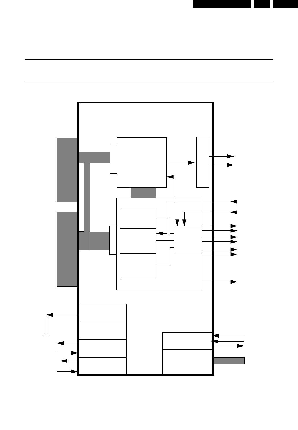
IC Descriptions. GB 51ASD-1 9.
DVDALAS2plus Advanced Analogue DVD
Signal Processor and Laser Supply TZA1033
DEVICE BLOCK DIAGRAM
Laser#1
Laser#2
Diode
Ampli?ers
Processing
DPD
Land/Groove
Swap
Dual Laser
Supply
Serial
I/Face
Push Pull
3 Beam
Tracking
Var Gain
Balanced
HF
Servo
Signals
OPU
Interface
Control
Interface
DVD
CD
D1-D6
MUX
FTC
Land
V & I references
Rext
Header
Offset
Data & header
Mute
compensations
MUX
FTC comp.

IC Descriptions.
GB 52 ASD-19.
DVDALAS2plus Advanced Analogue DVD
Signal Processor and Laser Supply TZA1033
PINNING
Name Pin Description
CD-A 1 CD pick up input A
CD-B 2 CD pick up input B
CD-C 3 CD pick up input C
CD-D 4 CD pick up input D
CD-REF 5 CD pick up reference voltage
CD-E 6 CD pick up input E
CD-F 7 CD pick up input F
DVD-A 12 DVD pick up input A
DVD-B 13 DVD pick up input B
DVD-C 14 DVD pick up input C
DVD-D 15 DVD pick up input D
DVD-ref 16 DVD pick up reference voltage
O-A 48 Servo current output for Focus-A
O-B 47 Servo current output for Focus-B
O-C 46 Servo current output for Focus-C
O-D 45 Servo current output for Focus-D
O-central 40 Testpin for offset cancelation
TD2 37 Internally connected
FTC-ref 36 Servo output voltage reference input
S1 42 Servo current output for radial tracking
S2 41 Servo current output for radial tracking
TD1 35 Internally connected
FTC 33 Fast track count voltage output
RFP 55 pos. RF output signal
RFN 56 neg. RF output signal
RF-REF 54 DC Reference signal input RF
LPF-DPD1 38 DPD Low pass bandwidth capacitor, channel pos
LPF-DPD2 39 DPD Low passbandwidth capacitor, channel neg
Land 20 Land/groove toggle input
HEADER 21 Header detector window input
CD-MI 62 CD laser monitor input
DVD-MI 10 DVD laser monitor input
CD-LO 61 CD laser output
DVD-LO 64 DVD laser output
COP 27 Positive inputFTC comparator
COM 28 Inverting inputFTC comparator
COO 29 FTC comparator output

IC Descriptions. GB 53ASD-1 9.
DVDALAS2plus Advanced Analogue DVD
Signal Processor and Laser Supply TZA1033
SIDA 23 Serial host interface data input
SICL 24 Serial host interface clock input
SILD 25 Serial host interface load
VDDA1 8 Analog Supply voltage 1 (RF input)
VDDA2 59 Analog Supply voltage 2 (RF internal)
VDDA3 53 Analog Supply voltage 3 (RF output stage)
VDDA4 44 Analog Supply voltage 4 (Servo)
VDDD5 30 Digital Supply voltage (5V dig core)
VDDD3 22 Digital Supply voltage (3V I/O pads and FTC comp.)
VDDL 63 Supply voltage for laser
VSSA1 9 Analog Ground 1
VSSA2 58 Analog Ground 2
VSSA3 57 Analog Ground 3
VSSA4 43 Analog Ground 4
VSSD 26 Digital ground
Rext 60 Reference current input (Connect 12k1 to VSSA4)
STB 31 Standby input
TM 19 Testmode input
TDO 34 test data out
Name Pin Description
IC Descriptions.
GB 54 ASD-19.
DVDALAS2plus Advanced Analogue DVD
Signal Processor and Laser Supply TZA1033
PINNING
Fig.2 Pin configuration.
handbook, full pagewidth
XXX
MXXxxx
1
2
3
4
5
6
7
8
9
10
11
12
13
14
15
16
48
47
46
45
44
43
42
41
40
39
38
37
36
35
34
33
17
18
19
20
21
22
23
24
25
26
27
28
29
30
31
32
64
63
62
61
60
59
58
57
56
55
54
53
52
51
50
49
NEW
CD-A
CD-C
CD-B
CD-D
CD-REF
CD-E
CD-F
VDDA1
VSSA1
DVD-MI
-
DVD-A
DVD-B
DVD-C
DVD-D
DVD-REF
TM
VSSD
COP
COM
COO
VDDD5
STB
-
LAND
HEADER
VDDD3
SIDA
SICL
SILD
-
-
FTC
TDO
TD1
FTC-REF
TD2
LPF-DPD1
LPF-DPD2
O-CENTRAL
S2
S1
VSSA4
VDDA4
O-D
O-C
O-B
O-A
VDDA3
VSSA3
CD-LO
R-EXT
VDDA2
VSSA2
DVD-LO
RFN
RFP
RF-REF
VDDL
CD-MI
-
-
-
-
TZA1023
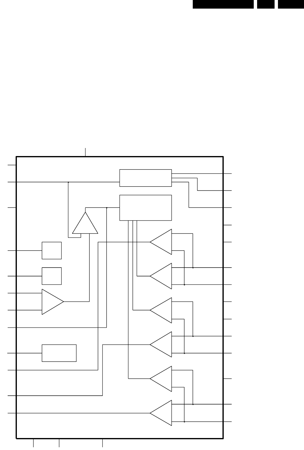
IC Descriptions. GB 55ASD-1 9.
BA6856FP: 3 PHASE MOTOR DRIVER FOR DVD PLAYERS
Features
• /3-phase, full-wave pseudo linear driving system
• built-in power save
• built-in therma shut down circuit
• built-in current limit circuit
• built in Hall bias circuit
• built in FG-output (3-phase parallel output)
• with switching function of regular/ reverse rotations
blockdiagram
-+
REV
PS
-
+
H BIAS
CONTROL
GAIN
DRIVER
+
-
+
-
+
-
+
-
+
-
+
-
MT1
29
MT2
30
NC1
NC2
NC3
NC4
NC5
PS
23
REV
24
RNF
28
VCC
25
VH
19
VM1
26
VM2
27
A1
A2
A3
CNF
20
EC
22
21
ECR
FG1
18
FG2
17
FG3
16
GND
8
H1+
H1-
H2+
H2-
H3+
H3-
BA6856FB
3
5
7
1
2
9
10
4
6
11
12
15
13
14
IC Descriptions.
GB 56 ASD-19.
pin description
PIN No PIN NAME DESCRIPTION
1 N.C. Not connected
2 N.C. Not connected
3A
3Output 3 for motor
4 N.C. Not connected
5A
2Output 2 for motor
6 N.C. Not connected
7A
1Output 1 for motor
8 GND Ground
9H
1
+Hall input Amp1. positive input
10 H1
-Hall input Amp1. negative input
11 H2
+Hall input Amp2. positive input
12 H2
-Hall input Amp2. negative input
13 H3
+Hall input Amp3. positive input
14 H3
-Hall input Amp3. negative input
15 N.C. Not connected
16 FG3 FG3 signal output terminal
17 FG2 FG2 signal output terminal
18 FG1 FG1 signal output terminal
19 VHHall Bias
20 CNF Capacitor connection pin for phase compensation
21 ECR Torque control standard voltage input terminal
22 ECTorque control voltage input terminal
23 PS POWER SAVE switch
24 REV Reverse terminal
25 VCC Power supply for sinal division
26 VM2 Power supply 2 for driver
27 VM1 Power supply 2 for driver
28 RNF Power supply for driver division
FIN FIN GND
Terminal lay-out
VM2
VCC
REV
PS
EC
ECR
CNF
VH
FG1
FG2
N.C.
A2
A1
GND
H1+
H1-
H2+
H2-
RNF
VM1
FG3
N.C.
H3+
H3-
N.C.
N.C.
N.C.
A3

IC Descriptions. GB 57ASD-1 9.
DSP for CD and DVD-ROM systems SAA7335
FEATURES
•Compatibility with CD-I, CD-ROM, MPEG-video
DVD-ROM and DVD-video applications
•Designed for very high playback speeds
•Typical CD-ROM operation up to n = 12, DVD-ROM to
n = 1.9, maximum rates (tbf)
•Matched filtering, quad-pass error correction
(C1-C2-C1-C2), overspeed audio playback function
included (up to 3 kbytes buffer)
•Lock-to-disc playback, Constant Angular Velocity
(CAV), pseudo-Constant Linear Velocity (CLV) and CLV
motor control loops
•Interface to 32 kbytes SRAM for DVD error correction
and de-interleave
•Sub-code/ header processing for DVD and CD formats
•Programmable HF equalizer
•In DVD mode it is still compatible with Philips block
decoders
•Sub-CPU interface can be parallel or fast I
2
C-bus
•On-chip clock multiplier.
GENERAL DESCRIPTION
This device is a high-end combined Compact Disc (CD)
and Digital Versatile Disc (DVD) compatible decoding
device. The device operates with an external 32 kbytes
S-RAM memory for de-interleaving operations. The device
provides quad-pass error correction for CD-ROM
applications (C1-C2-C1-C2) and operates in lock-to-disk,
CAV, pseudo CLV and CLV modes.
In DVD modes double-pass C1-C2 error correction is used
which is capable of correcting up to 5 C1 frame errors and
16 C2 frame errors.
The SAA7335 contains all the functions required to
decode an EFM or EFM+ HF signal directly from the laser
pre-amplifier, including analog front-end, PLL data
recovery, demodulation and error correction. The spindle
motor interface provides both motor control signals from
the demodulator and, in addition, contains a tachometer
loop that accepts tachometer pulses from the motor unit.
The SAA7335 has two independent microcontroller
interfaces. The first is a serial I
2
C-bus and the second is a
standard 8-bit multiplexed parallel interface. Both of these
interfaces provide access to a total of 32 ×8-bit registers
for control and status.
This data sheet contains an descriptive overview of the
device together with electrical and timing characteristics.
For a detailed description of the device refer to the user
guide
“SAU/UM96018”
.
Supply of this CD/DVD IC does not convey an implied
license under any patent right to use this IC in any CD or
DVD application.
QUICK REFERENCE DATA
SYMBOL PARAMETER MIN. TYP. MAX. UNIT
V
DDD
digital supply voltage 4.5 5.0 5.5 V
I
DDD
digital supply current −70 300 mA
V
DDA
analog supply voltage 4.5 5.0 5.5 V
I
DDA
analog supply current −70 300 mA
f
xtal
crystal input frequency 4 25 tbf MHz
T
amb
operating ambient temperature −20 −+70 °C
T
stg
storage temperature −55 −+125 °C
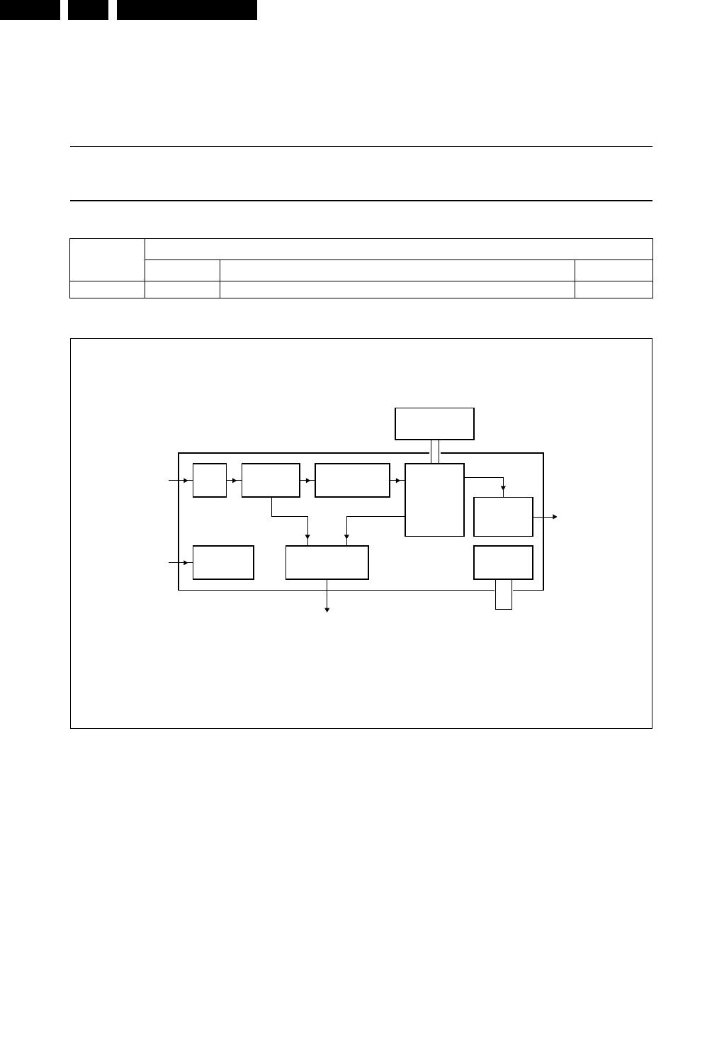
IC Descriptions.
GB 58 ASD-19.
DSP for CD and DVD-ROM systems SAA7335
ORDERING INFORMATION
BLOCK DIAGRAM
TYPE
NUMBER
PACKAGE
NAME DESCRIPTION VERSION
SAA7335GP LQFP100 plastic low pro?le quad ?at package; 100 leads; body 14 ×14 ×1.4 mm SOT407-1
Fig.1 Simplified block diagram.
handbook, full pagewidth
MGK242
DEMODULATOR
EFM/EFM+
PLL BIT
DETECTOR
SRAM
32 KBYTES
SPINDLE
MOTOR CONTROL
motor control
SAA7335
CLOCK
GENERATOR
SUB-CPU
INTERFACE
ADCHF input
clock input
DECODER block
decoder
output
I
2
S-BUS
OUTPUT
INTERFACE

IC Descriptions. GB 59ASD-1 9.
DSP for CD and DVD-ROM systems SAA7335
PINNING
SYMBOL PIN TYPE DESCRIPTION
V
SSA1
1 supply analog ground 1
I
ref
2 I analog current reference input for ADC
REFLo 3 I analog low reference input for ADC
REFHi 4 I analog high reference input for ADC
VREF 5 I analog negative input
HFIN 6 I analog positive input
V
SSA2
7 supply analog ground 2
AGCOUT 8 O analog test pin output
V
DDA2
9 supply analog supply voltage 2
V
DDD1
10 supply digital supply voltage 1
V
SSD1
11 supply digital ground 1
OTD 12 I off track detect input
MOTO1 13 O 3-state motor control output
n.c. 14 −not connected, reserved
MOTO2/T3 15 I/O motor control output/tachometer 3 input
n.c. 16 −not connected, reserved
T1 17 I tachometer 1 input
T2 18 I tachometer 2 input
V
DDD2
19 supply digital supply voltage 2
V
SSD2
20 supply digital ground 2
TEST1 21 I test input 1
TEST2 22 I test input 2
POR 23 I power-on reset input
MUXSWICH 24 I use clock multiplier input
n.c. 25 −not connected, reserved
CL1 26 O divided clock output
BCAIN 27 I BCA input
SDA 28 I/O sub-CPU I
2
C-bus serial data input/output
SCL 29 I sub-CPU I
2
C-bus serial clock input
INT 30 O sub-CPU interrupt output (open-drain)
V
DDD3
31 supply digital supply voltage 3
V
SSD3
32 supply digital ground 3
da7 33 I/O sub-CPU data bus bit 7 input/output (parallel)
da6 34 I/O sub-CPU data bus bit 6 input/output (parallel)
da5 35 I/O sub-CPU data bus bit 5 input/output (parallel)
n.c. 36 −not connected, reserved
da4 37 I/O sub-CPU data bus bit 4 input/output (parallel)
n.c. 38 −not connected, reserved
da3 39 I/O sub-CPU data bus bit 3 input/output (parallel)
da2 40 I/O sub-CPU data bus bit 2 input/output (parallel)

IC Descriptions.
GB 60 ASD-19.
DSP for CD and DVD-ROM systems SAA7335
da1 41 I/O sub-CPU data bus bit 1 input/output (parallel)
n.c. 42 −not connected, reserved
da0 43 I/O sub-CPU data bus bit 0 input/output (parallel)
V
DDD4
44 supply digital supply voltage 4
V
SSD4
45 supply digital ground 4
WRi 46 I sub-CPU write enable input (active LOW)
RDi 47 I sub-CPU read enable input (active LOW)
ALE 48 I sub-CPU address latch enable input
CSi 49 I sub-CPU chip select input (active HIGH)
STOPCLOCK 50 O stop clock output
n.c. 51 −not connected, reserved
V4 52 O serial subcode output (for CD)
EBUOUT 53 O digital audio output
SYNC 54 O I
2
S-bus sector sync output
FLAG 55 O I
2
S-bus correction ?ag output
DATA 56 O I
2
S-bus serial data output
BCLK 57 I/O I
2
S-bus bit serial clock input/output
WCLK 58 I/O I
2
S-bus word clock input/output
V
DDD5
59 supply digital supply voltage 5
V
SSD5
60 supply digital ground 5
RAMRW 61 O RAM read/write control output
n.c. 62 −not connected, reserved
RAMDA7 63 I/O RAM data bus bit 7 input/output
RAMDA6 64 I/O RAM data bus bit 6 input/output
RAMDA5 65 I/O RAM data bus bit 5 input/output
RAMDA4 66 I/O RAM data bus bit 4 input/output
RAMDA3 67 I/O RAM data bus bit 3 input/output
RAMDA2 68 I/O RAM data bus bit 2 input/output
n.c. 69 −not connected, reserved
RAMDA1 70 I/O RAM data bus bit 1 input/output
RAMDA0 71 I/O RAM data bus bit 0 input/output
V
DDD6
72 supply digital supply voltage 6
V
SSD6
73 supply digital ground 6
RAMAD0 74 O RAM address bit 0 output
RAMAD1 75 O RAM address bit 1 output
RAMAD2 76 O RAM address bit 2 output
RAMAD3 77 O RAM address bit 3 output
RAMAD4 78 O RAM address bit 4 output
RAMAD5 79 O RAM address bit 5 output
RAMAD6 80 O RAM address bit 6 output
V
DDD7
81 supply digital supply voltage 7
SYMBOL PIN TYPE DESCRIPTION

IC Descriptions. GB 61ASD-1 9.
DSP for CD and DVD-ROM systems SAA7335
V
SSD7
82 supply digital ground 7
RAMAD7 83 O RAM address bit 7 output
RAMAD8 84 O RAM address bit 8 output
RAMAD9 85 O RAM address bit 9 output
n.c. 86 −not connected, reserved
RAMAD10 87 O RAM address bit 10 output
RAMAD11 88 O RAM address bit 11 output
RAMAD12 89 O RAM address bit 12 output
RAMAD13 90 O RAM address bit 13 output
RAMAD14 91 O RAM address bit 14 output
V
DDD8
92 supply digital supply voltage 8
V
SSD8
93 supply digital ground 8
CRIN 94 I analog crystal input
CROUT 95 O analog crystal output
CFLG 96 O correction statistics output
MEAS1 97 O front-end telemetry output
V
DDD9
98 supply digital supply voltage 9
V
SSD9
99 supply digital ground 9
V
DDA1
100 supply analog supply voltage 1
SYMBOL PIN TYPE DESCRIPTION
IC Descriptions.
GB 62 ASD-19.
DSP for CD and DVD-ROM systems SAA7335
Fig.2 Pin configuration.
handbook, full pagewidth
75
74
73
72
71
70
69
68
67
66
65
64
63
62
61
60
59
58
57
56
55
54
53
52
51
80
79
78
77
76
RAMAD1
RAMAD0
VSSD6
VDDD6
RAMDA0
RAMDA1
n.c.
RAMDA2
RAMDA3
RAMDA4
RAMDA5
RAMDA6
RAMDA7
n.c.
RAMRW
VSSD5
VDDD5
WCLK
BCLK
DATA
FLAG
SYNC
EBUOUT
V4
n.c.
MGK241
VSSA1
Iref
REFLo
REFHi
VREF
HFIN
VSSA2
AGCOUT
VDDA2
VDDD1
VSSD1
OTD
MOTO1
n.c.
MOTO2/T3
n.c.
T1
T2
VDDD2
VSSD2
TEST1
TEST2
POR
MUXSWICH
n.c.
RAMAD6
RAMAD5
RAMAD4
RAMAD3
RAMAD2
VDDA1
VSSD9
VDDD9
MEAS1
CFLG
CROUT
CRIN
VSSD8
VDDD8
RAMAD14
RAMAD13
RAMAD12
RAMAD11
RAMAD10
n.c.
RAMAD9
RAMAD8
RAMAD7
VSSD7
VDDD7
VDDD3
VSSD3
da7
da6
da5
n.c.
da4
n.c.
da3
da2
da1
n.c.
da0
VDDD4
VSSD4
WRi
RDi
ALE
CSi
STOPCLOCK
CL1
BCAIN
SDA
SCL
INT 30
29
28
27
26
25
24
23
22
21
20
19
18
17
16
15
14
13
12
11
10
9
8
7
6
5
4
3
2
1
100
99
98
97
96
95
94
93
92
91
90
89
88
87
86
85
84
83
82
81
31
32
33
34
35
36
37
38
39
40
41
42
43
44
45
46
47
48
49
50
SAA7335

IC Descriptions. GB 63ASD-1 9.
DSP for CD and DVD-ROM systems SAA7335
FUNCTIONAL DESCRIPTION
Analog front-end
This block converts the HF input to the digital domain using
an 8-bit ADC proceeded by an AGC circuit to obtain the
optimum performance from the convertor. This block is
clocked by ADCCLK which is set by the external crystal
frequency plus a flexible clock multiplier and divider block.
PLL and bit detector
This subsystem recovers the data from the channel
stream. The block corrects asymmetry, performs noise
filtering and equalisation and finally recovers the bit clock
and data from the channel using a digital PLL.
The equalizer and the data slicer are programmable.
Digital logic
All the digital system logic is clocked from the master ADC
clock (ADCCLK) described above.
Advanced bit detector
The advanced bit detector offers improved data recovery
for multi-layer discs and contains two extra detection
circuits to increase the margins in the bit recovery block:
1. Adaptive slicer: adds a second stage slicer with higher
bandwidth
2. Run length 2 push-back: all T2 run lengths are pushed
back to T3, thereby automatically determining the
erroneous edge and shifting the transitions on that
edge.
Demodulator
F
RAME SYNC PROTECTION
CD
MODE
This circuit detects the frame synchronization signals.
Two synchronization counters are used in the SAA7335:
1. The coincidence counter: this is used to detect the
coincidence of successive syncs. It generates a sync
coincidence signal if 2 syncs are 588 ±1 EFM clocks
apart.
2. The main counter: this is used to partition the EFM
signal into 17-bit words. This counter is reset when:
a) A sync coincidence is generated
b) A sync is found within ±6 EFM clocks of its
expected position.
The sync coincidence signal is also used to generate the
lock signal which will go active HIGH when 1 sync
coincidence is found. It will reset to LOW when, during
61 consecutive frames, no sync coincidence is found.
F
RAME SYNC PROTECTION
DVD
MODE
This circuit detects the frame synchronization signals.
Two synchronization counters are used in the SAA7335:
1. The coincidence counter: this is used to detect the
coincidence of successive syncs. It generates a sync
coincidence signal if 2 syncs are 1488 ±3 EFM+
clocks apart.
2. The main counter: this is used to partition the EFM+
signal into 16-bit words. This counter is reset when:
a) A sync coincidence is generated
b) A sync is found within ±10 EFM+ clocks of its
expected position.
The sync coincidence signal is also used to generate the
lock signal which will go active HIGH when 1 sync
coincidence is found. It will reset to LOW when, during
61 consecutive frames, no sync coincidence is found.
EFM/EFM+ demodulation
The 14-bit EFM (16-bit EFM+) data and subcode words
are decoded into 8-bit symbols.

IC Descriptions.
GB 64 ASD-19.
DSP for CD and DVD-ROM systems SAA7335
Microcontroller interface
The SAA7335 has two microcontroller interfaces, one
serial I
2
C-bus and one parallel (8051 microcontroller
compatible).
The two communication modes may be operated at the
same time, the modes are described below:
1. Parallel mode: protocol compatible with 8052
multiplexed bus:
a) da0 to da7 = address/data bus
b) ALE = Address Latch Enable, latches the address
information on the bus
c) WRi = active LOW write signal for write to
SAA7335
d) RDi = active LOW read signal for read from
SAA7335
e) CSi = active HIGH Chip Select signal (this signal
gates the RDi and WRi signals).
2. I
2
C-bus mode: I
2
C-bus protocol where SAA7335
behaves as slave device where:
a) SDA = I
2
C-bus data
b) SCL = I
2
C-bus clock
c) I
2
C-bus slave address (write mode) = 3EH
d) I
2
C-bus slave address (read mode) = 3FH
e) Maximum data transfer rate = 400 kbits/s.
M
ICROCONTROLLER INTERFACE
(I
2
C-
BUS MODE
)
Bytes are transferred over the interface in single bytes of
which there are two types; write data commands and read
data commands.
The sequence for a write data command (1 data byte) is as
follows:
•Send START condition
•Send address 3EH (write)
•Write command address byte
•Write data byte
•Send STOP condition.
The sequence for a read data command (that reads 1 data
byte) is as follows:
•Send START condition
•Send address 3EH (write)
•Write status address byte
•Send STOP condition
•Send START condition
•Send address 3FH (read)
•Read data byte
•Send STOP condition.
R
EADING AND WRITING DATA TO THE
SAA7335
The SAA7335 has 32 ×8-bit configuration and status
registers as shown in Table 1. Not all locations are
currently defined and some remain reserved for future
upgrades. These can be written to or read from via the
microcontroller interface using either the serial or parallel
control bus.

IC Descriptions. GB 65ASD-1 9.
Am29LV160BT/Am29LV160BB
16 Megabit (2 M x 8-Bit/1 M x 16-Bit)
CMOS 3.0 Volt-only Sector Erase Flash Memory
DISTINCTIVE CHARACTERISTICS
■Single power supply operation
—Full voltage range: 2.7 to 3.6 volt read and write
operations for battery-powered applications
—Regulated voltage range: 3.0 to 3.6 volt read
and write operations and for compatibility with
high performance 3.3 volt microprocessors
■Manufactured on 0.35 µm process technology
■Supports Common Flash Memory Interface
(CFI)
■High performance
—Full voltage range: access times as fast as 90 ns
—Regulated voltage range: access times as fast
as 80 ns
■Ultra low power consumption (typical values at
5 MHz)
—200 nA Automatic Sleep mode current
—200 nA standby mode current
—10 mA read current
—20 mA program/erase current
■Flexible sector architecture
—One 16 Kbyte, two 8 Kbyte, one 32 Kbyte, and
thirty-one 64 Kbyte sectors (byte mode)
—One 8 Kword, two 4 Kword, one 16 Kword, and
thirty-one 32 Kword sectors (word mode)
—Supports full chip erase
—Sector Protection features:
A hardware method of locking a sector to
prevent any program or erase operations within
that sector
Sectors can be locked in-system or via
programming equipment
Temporary Sector Unprotect feature allows code
changes in previously locked sectors
■Top or bottom boot block configurations
available
■Embedded Algorithms
—Embedded Erase algorithm automatically
preprograms and erases the entire chip or any
combination of designated sectors
—Embedded Program algorithm automatically
writes and verifies data at specified addresses
■Minimum 100,000 write cycle guarantee per
sector
■Package option
—48-ball FBGA
—48-ball µBGA
—48-pin TSOP
—44-pin SO
■Compatibility with JEDEC standards
—Pinout and software compatible with single-
power supply Flash
—Superior inadvertent write protection
■Data# Polling and toggle bits
—Provides a software method of detecting
program or erase operation completion
■Ready/Busy# pin (RY/BY#)
—Provides a hardware method of detecting
program or erase cycle completion (not
available on 44-pin SO)
■Erase Suspend/Erase Resume
—Suspends an erase operation to read data from,
or program data to, a sector that is not being
erased, then resumes the erase operation
■Hardware reset pin (RESET#)
—Hardware method to reset the device to reading
array data

IC Descriptions.
GB 66 ASD-19.
GENERAL DESCRIPTION
The Am29LV160B is a 16 Mbit, 3.0 Volt-only Flash
memory organized as 2,097,152 bytes or 1,048,576
words. The device is offered in 48-ball FBGA, 48-ball
µBGA, 44-pin SO, and 48-pin TSOP packages. The
word-wide data (x16) appears on DQ15–DQ0; the byte-
wide (x8) data appears on DQ7–DQ0. This device is
designed to be programmed in-system with the standard
system 3.0 volt V
CC
supply. A 12.0 V V
PP
or 5.0 V
CC
are
not required for write or erase operations. The device can
also be programmed in standard EPROM programmers.
The device offers access times of 80, 90, and 120 ns,
allowing high speed microprocessors to operate
without wait states. To eliminate bus contention the
device has separate chip enable (CE#), write enable
(WE#) and output enable (OE#) controls.
The device requires only a single 3.0 volt power sup-
ply for both read and write functions. Internally gener-
ated and regulated voltages are provided for the
program and erase operations.
The Am29LV160B is entirely command set compatible
with the JEDEC single-power-supply Flash stan-
dard. Commands are written to the command register
using standard microprocessor write timings. Register
contents serve as input to an internal state-machine
that controls the erase and programming circuitry.
Write cycles also internally latch addresses and data
needed for the programming and erase operations.
Reading data out of the device is similar to reading
from other Flash or EPROM devices.
Device programming occurs by executing the program
command sequence. This initiates the Embedded
Program algorithm—an internal algorithm that auto-
matically times the program pulse widths and verifies
proper cell margin. The Unlock Bypass mode facili-
tates faster programming times by requiring only two
write cycles to program data instead of four.
Device erasure occurs by executing the erase com-
mand sequence. This initiates the Embedded Erase
algorithm—an internal algorithm that automatically pre-
programs the array (if it is not already programmed) be-
fore executing the erase operation. During erase, the
device automatically times the erase pulse widths and
verifies proper cell margin.
The host system can detect whether a program or
erase operation is complete by observing the RY/BY#
pin, or by reading the DQ7 (Data# Polling) and DQ6
(toggle) status bits. After a program or erase cycle
has been completed, the device is ready to read array
data or accept another command.
The sector erase architecture allows memory sectors
to be erased and reprogrammed without affecting the
data contents of other sectors. The device is fully
erased when shipped from the factory.
Hardware data protection measures include a low V
CC
detector that automatically inhibits write operations dur-
ing power transitions. The hardware sector protection
feature disables both program and erase operations in
any combination of the sectors of memory. This can be
achieved in-system or via programming equipment.
The Erase Suspend/Erase Resume feature enables
the user to put erase on hold for any period of time to
read data from, or program data to, any sector that is
not selected for erasure. True background erase can
thus be achieved.
The hardware RESET# pin terminates any operation
in progress and resets the internal state machine to
reading array data. The RESET# pin may be tied to the
system reset circuitry. A system reset would thus also
reset the device, enabling the system microprocessor
to read the boot-up firmware from the Flash memory.
The device offers two power-saving features. When
addresses have been stable for a specified amount of
time, the device enters the automatic sleep mode.
The system can also place the device into the standby
mode. Power consumption is greatly reduced in both
these modes.
AMD's Flash technology combines years of Flash memory
manufacturing experience to produce the highest levels of
quality, reliability and cost effectiveness. The device electri-
cally erases all bits within a sector simultaneously
via Fowler-Nordheim tunneling. The data is programmed
using hot electron injection.
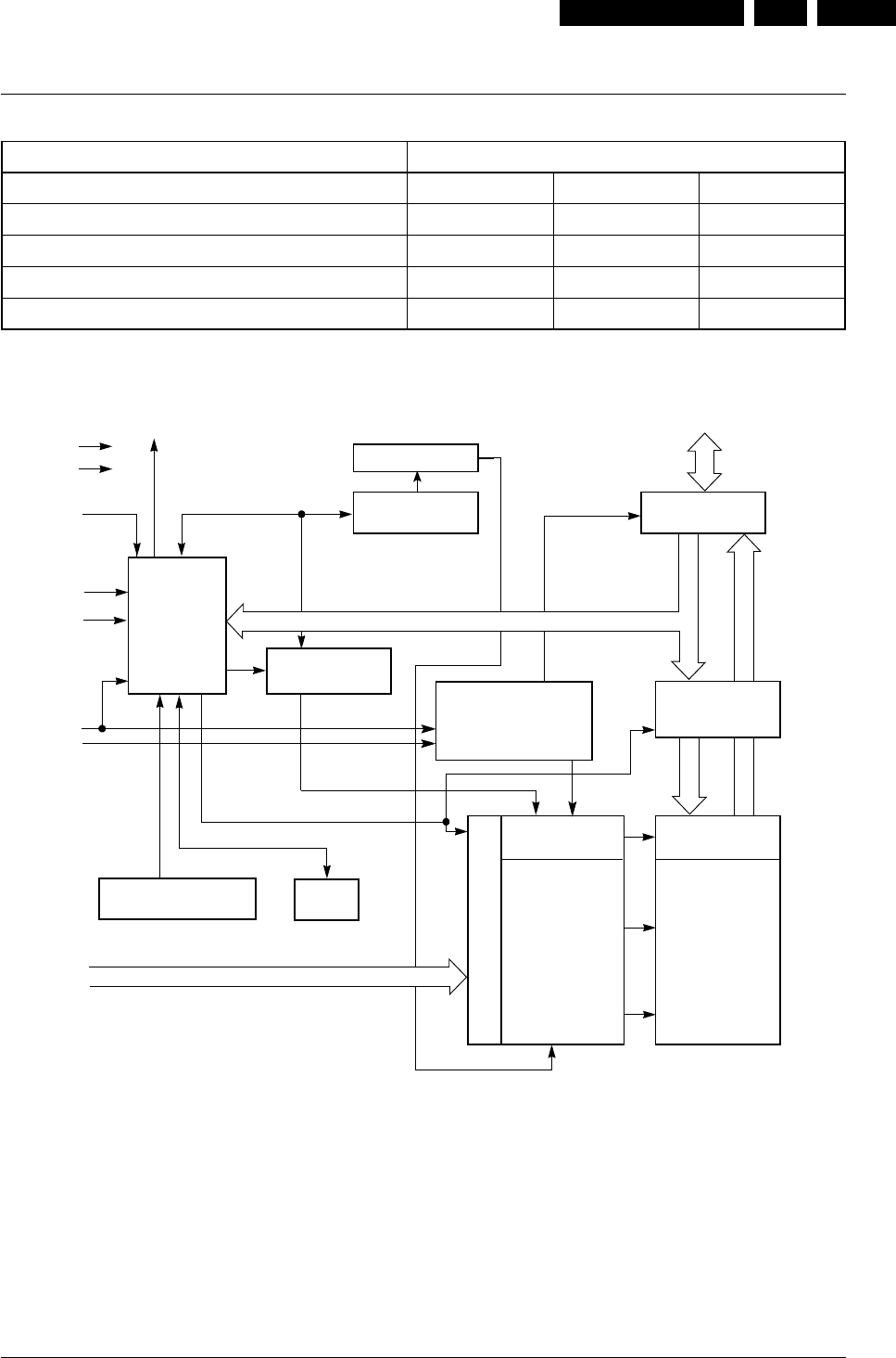
IC Descriptions. GB 67ASD-1 9.
PRODUCT SELECTOR GUIDE
Note: See “AC Characteristics” for full specifications.
BLOCK DIAGRAM
Family Part Number Am29LV160B
Ordering Part Number: VCC =3.0–3.6 V 80R
V
CC = 2.7–3.6 V 90 120
Max access time, ns (tACC)80 90 120
Max CE# access time, ns (tCE)80 90 120
Max OE# access time, ns (tOE)30 35 50
Input/Output
Buffers
X-Decoder
Y-Decoder
Chip Enable
Output Enable
Logic
Erase Voltage
Generator
PGM Voltage
Generator
Timer
VCC Detector
State
Control
Command
Register
VCC
VSS
WE#
BYTE#
CE#
OE#
STB
STB
DQ0
–
DQ15 (A-1)
Sector Switches
RY/BY#
RESET#
Data
Latch
Y-Gating
Cell Matrix
Address Latch
A0–A19
21358C-1
IC Descriptions.
GB 68 ASD-19.
CONNECTION DIAGRAMS
A1
A15
A18
A14
A13
A12
A11
A10
A9
A8
A19
NC
WE#
RESET#
NC
NC
RY/BY#
A17
A7
A6
A5
A4
A3
A2
1
16
2
3
4
5
6
7
8
17
18
19
20
21
22
23
24
9
10
11
12
13
14
15
A16
DQ2
BYTE#
V
SS
DQ15/A-1
DQ7
DQ14
DQ6
DQ13
DQ9
DQ1
DQ8
DQ0
OE#
V
SS
CE#
A0
DQ5
DQ12
DQ4
V
CC
DQ11
DQ3
DQ10
48
33
47
46
45
44
43
42
41
40
39
38
37
36
35
34
25
32
31
30
29
28
27
26
21358C-2
Reverse TSOP
Standard TSOP
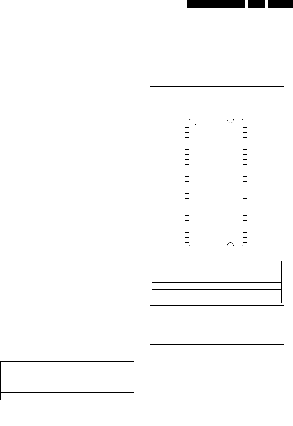
IC Descriptions. GB 69ASD-1 9.
KEY TIMING PARAMETERS
SPEED CLOCK ACCESS TIME SETUP HOLD
CL = 3**
-6 166 MHz 5.5ns 2ns 1ns
-7 143 MHz 5.5ns 2ns 1ns
-8A 125 MHz 6ns 2ns 1ns
*Off-center parting line
**CL = CAS (READ) latency
1 Meg x 16
Configuration 512K x 16 x 2 banks
Refresh Count 2K or 4K
Row Addressing 2K (A0-A10)
Bank Addressing 2 (BA)
Column Addressing 256 (A0-A7)
SYNCHRONOUS
DRAM
MT48LC1M16A1 S - 512K x 16 x 2 banks
PIN ASSIGNMENT (Top View)
50-Pin TSOP
FEATURES
• PC100 functionality
• Fully synchronous; all signals registered on positive
edge of system clock
• Internal pipelined operation; column address can be
changed every clock cycle
• Internal banks for hiding row access/precharge
1 Meg x 16 - 512K x 16 x 2 banks architecture with
11 row, 8 column addresses per bank
• Programmable burst lengths: 1, 2, 4, 8 or full page
• Auto Precharge Mode, includes CONCURRENT
AUTO PRECHARGE
• Self Refresh and Adaptable Auto Refresh Modes
- 32ms, 2,048-cycle refresh or
- 64ms, 2,048-cycle refresh or
- 64ms, 4,096-cycle refresh
• LVTTL-compatible inputs and outputs
• Single +3.3V ±0.3V power supply
• Supports CAS latency of 1, 2 and 3
OPTIONS MARKING
• Configuration
1 Meg x 16 (512K x 16 x 2 banks) 1M16A1
• Plastic Package - OCPL*
50-pin TSOP (400 mil) TG
• Timing (Cycle Time)
6ns (166 MHz) -6
7ns (143 MHz) -7
8ns (125 MHz) -8A
• Refresh
2K or 4K with Self Refresh Mode at 64ms S
• Part Number Example: MT48LC1M16A1TG-7S
Note: The # symbol indicates signal is active LOW.
VDD
DQ0
DQ1
VssQ
DQ2
DQ3
VDDQ
DQ4
DQ5
VssQ
DQ6
DQ7
VDDQ
DQML
WE#
CAS#
RAS#
CS#
BA
A10
A0
A1
A2
A3
VDD
12345678910111213141516171819202122232425
50494847464544434241403938373635343332313029282726
Vss
DQ15
DQ14
VssQ
DQ13
DQ12
VDDQ
DQ11
DQ10
VssQ
DQ9
DQ8
VDDQ
NC
DQMH
CLK
CKE
NC
A9
A8
A7
A6
A5
A4
Vss
16Mb (x16) SDRAM PART NUMBER
PART NUMBER ARCHITECTURE
MT48LC1M16A1TG S 1 Meg x 16
GENERAL DESCRIPTION
The 16Mb SDRAM is a high-speed CMOS, dynamic
random-access memory containing 16,777,216 bits. It is
internally configured as a dual 512K x 16 DRAM with a
synchronous interface (all signals are registered on the
positive edge of the clock signal, CLK). Each of the 512K x
16-bit banks is organized as 2,048 rows by 256 columns by
16 bits. Read and write accesses to the SDRAM are burst
oriented; accesses start at a selected location and continue
for a programmed number of locations in a programmed

IC Descriptions.
GB 70 ASD-19.
16Mb: x16
SDRAM
G EN ERAL DESCRIPTIO N (continued) but it also allows the column address to be changed on every
clock cycle to achieve a high-speed, fully random access.
Precharging one bank while accessing the alternate bank
will hide the PRECHARGE cycles and provide seamless,
high-speed, random-access operation.
The 1 Meg x 16 SDRAM is designed to operate in 3.3V,
low-power memory systems. An auto refresh mode is
provided, along with a power-saving, power-down mode.
All inputs and outputs are LVTTL-compatible.
SDRAMs offer substantial advances in DRAM operat-
ing performance, including the ability to synchronously
burst data at a high data rate with automatic column-
address generation, the ability to interleave between inter-
nal banks in order to hide precharge time, and the capability
to randomly change column addresses on each clock cycle
during a burst access.
sequence. Accesses begin with the registration of an AC-
TIVE command, which is then followed by a READ or
WRITE command. The address bits registered coincident
with the ACTIVE command are used to select the bank and
row to be accessed (BA selects the bank, A0-A10 select the
row). The address bits registered coincident with the READ
or WRITE command are used to select the starting column
location for the burst access.
The SDRAM provides for programmable READ or
WRITE burst lengths of 1, 2, 4 or 8 locations, or the full page,
with a burst terminate option. An AUTO PRECHARGE
function may be enabled to provide a self-timed row
precharge that is initiated at the end of the burst sequence.
The 1 Meg x 16 SDRAM uses an internal pipelined
architecture to achieve high-speed operation. This architec-
ture is compatible with the 2n rule of prefetch architectures,
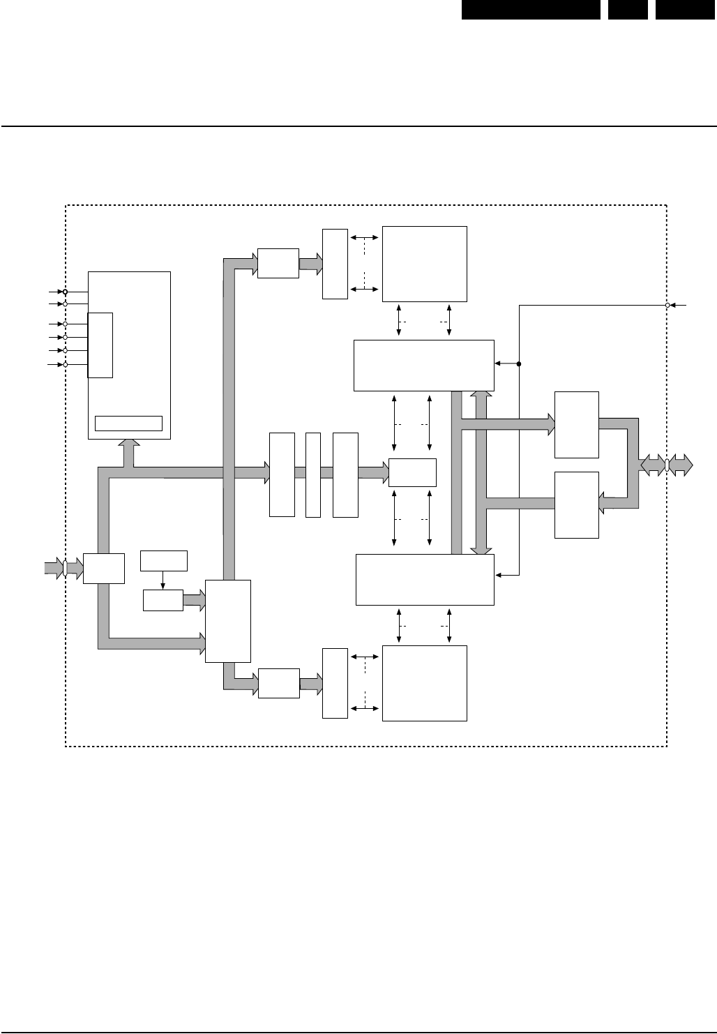
IC Descriptions. GB 71ASD-1 9.
16Mb: x16
SDRAM
11
11
11
RAS#
REFRESH
CONTROLLER
2,048
REFRESH
COUNTER
CAS#
256
256 (x16)
8
COLUMN-
ADDRESS BUFFER
BURST COUNTER
ROW-
ADDRESS
MUX
CLK
CS#
WE#
CKE
256 (x16)
BANK1
MEMORY
ARRAY
(2,048 x 256 x 16)
SENSE AMPLIFIERS
I/O GATING
DQM MASK LOGIC
CONTROL
LOGIC
COLUMN
DECODER
COLUMN-
ADDRESS LATCH
8
MODE REGISTER
ROW-
ADDRESS
LATCH
11
ROW
DECODER
11
COMMAND
DECODE
DQ0-
DQ15
A0-A10, BA
16
8
DQML,
DQMH
256
2,048
BANK0
MEMORY
ARRAY
(2,048 x 256 x 16)
ROW
DECODER
ROW-
ADDRESS
LATCH
11
12
ADDRESS
REGISTER
12
SENSE AMPLIFIERS
I/O GATING
DQM MASK LOGIC
DATA
INPUT
REGISTER
DATA
OUTPUT
REGISTER
16
16
FUNCTIONAL BLOCK DIAGRAM
1 Meg x 16 SDRAM

IC Descriptions.
GB 72 ASD-19.
16Mb: x16
SDRAM
PIN DESCRIPTIONS
PIN NUM BERS SYM BOL TYPE DESCRIPTION
35 CLK Input Clock: CLK is driven by the system clock. All SDRAM input signals are
sampled on the positive edge of CLK. CLK also increments the internal burst
counter and controls the output registers.
34 CKE Input Clock Enable: CKE activates (HIGH) and deactivates (LOW) the CLK signal.
Deactivating the clock provides PRECHARGE POWER-DOWN and SELF
REFRESH operations (all banks idle), ACTIVE POWER-DOWN (row ACTIVE
in either bank) or CLOCK SUSPEND operation (burst/access in progress).
CKE is synchronous except after the device enters power-down and self
refresh modes, where CKE becomes asynchronous until after exiting the
same mode. The input buffers, including CLK, are disabled during power-
down and self refresh modes, providing low standby power. CKE may be tied
HIGH.
18 CS# Input Chip Select: CS# enables (registered LOW) and disables (registered HIGH)
the command decoder. All commands are masked when CS# is registered
HIGH. CS# provides for external bank selection on systems with multiple
banks. CS# is considered part of the command code.
15, 16, 17 WE#, CAS#, Input Command Inputs: RAS#, CAS# and WE# (along with CS#) define the
RAS# command being entered.
14, 36 DQML, Input Input/Output Mask: DQM is an input mask signal for write accesses and an
DQMH output enable signal for read accesses. Input data is masked when DQM is
sampled HIGH during a WRITE cycle. The output buffers are placed in a
High-Z state (two-clock latency) when DQM is sampled HIGH during a READ
cycle. DQML corresponds to DQ0-DQ7; DQMH corresponds to DQ8-DQ15.
DQML and DQMH are considered same state when referenced as DQM.
19 BA Input Bank Address Inputs: BA defines to which bank the ACTIVE, READ, WRITE
or PRECHARGE command is being applied. BA is also used to program the
twelfth bit of the Mode Register.
21-24, 27-32, 20 A0-A10 Input Address Inputs: A0-A10 are sampled during the ACTIVE command (row-
address A0-A10) and READ/WRITE command (column-address A0-A7, with
A10 defining AUTO PRECHARGE) to select one location out of the 512K
available in the respective bank. A10 is sampled during a PRECHARGE
command to determine if all banks are to be precharged (A10 HIGH). The
address inputs also provide the op-code during a LOAD MODE REGISTER
command.
2, 3, 5, 6, 8, 9, DQ0- Input/ Data I/Os: Data bus.
11, 12, 39, 40, 42, DQ15 Output
43, 45, 46, 48, 49
33, 37 NC –No Connect: These pins should be left unconnected.
7, 13, 38, 44 V
DD
Q Supply DQ Power: Provide isolated power to DQs for improved noise immunity.
4, 10, 41, 47 V
SS
Q Supply DQ Ground: Provide isolated ground to DQs for improved noise immunity.
1, 25 V
DD
Supply Power Supply: +3.3V ±0.3V.
26, 50 V
SS
Supply Ground.
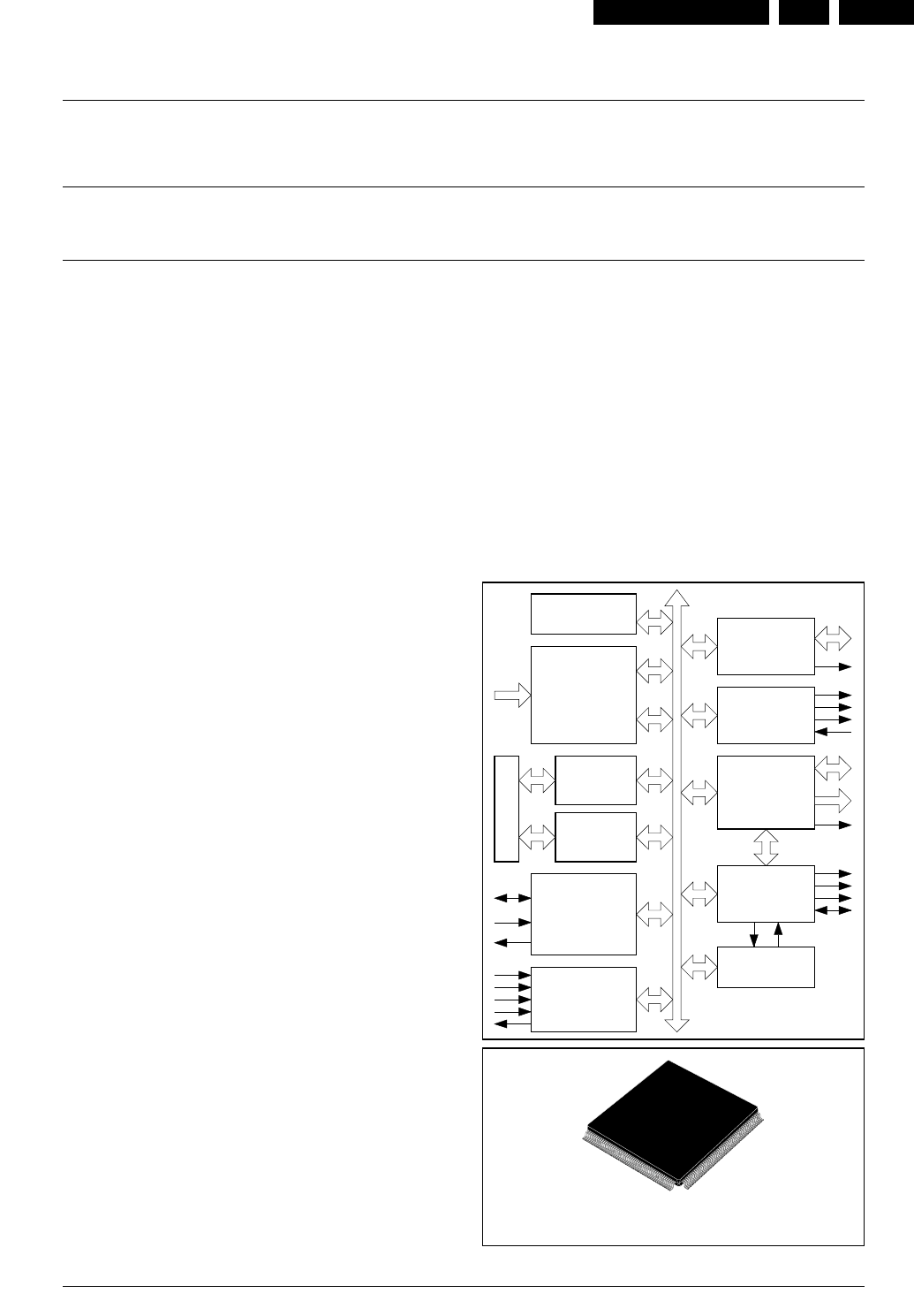
IC Descriptions. GB 73ASD-1 9.
PRODUCT PREVIEW
PQFP208 (Plastic Quad Flat Pack)
ORDER CODE : STi5505ACV
STi5505 (Rev. Ax)
DVD BACKEND DECODER
WITH INTEGRATED HOST PROCESSOR
.INTEGRATED 32-BIT RISC HOST CPU
- 2KBYTES INSTRUCTION CACHE, 2KBYTES
DATA CACHE/SRAM
- 50K DHRYSTONES/SEC (2.1) - 50MHz
.VIDEO DECODER
- FULLY SUPPORTS MPEG-2 MP@ML
- MEMORY REDUCTION - PAL IN 12MBITS
.SUBPICTURE DECODER
.HIGH PERFORMANCE ON-SCREEN DISPLAY
.AUDIO DECODER
- 5.1 CHANNEL DOLBY AC-3® / MULTI
CHANNEL MPEG-2 DECODING
- DOWNMIX TO STEREO OR TO DOLBY
PRO-LOGIC COMPATIBLE OUTPUTS FOR
MPEG-2 AND AC-3
- IEC6958 - IEC61937 COMPATIBLE OUTPUT
- LPCM (DVD) MODE SUPPORTED
- 6 CHANNELS OUTPUT
.PAL/NTSC ENCODER
- MACROVISION
TM
7.01/6.1 COMPATIBLE
- TELETEXT, AND CLOSED CAPTION
.HIGH PERFORMANCE SDRAM INTERFACE
.PROGRAMMABLE MEMORY INTERFACE
FOR DRAM, ROM, PERIPHERALS ETC.
.FRONT-END CHANNEL IC INTERFACE
- DVD, VCD AND CD-DA COMPATIBLE
- DSS - DVB BISTREAMS
- SERIAL AND PARALLEL INTERFACES
- HARDWARE SECTOR FILTERING
- INTEGRATED CSS DECRYPTION AND
TRACK BUFFER
.INTEGRATED PERIPHERALS
- 2 UARTS, 1 I
2
C CONTROLLER, 3 PWM OUT-
PUTS, 3 TIMERS, 3 CAPTURE TIMERS,
SMART CARD
- 34 BITS OF PROGRAMMABLE I/O
-OS LINK
.PROFESSIONAL TOOLSET SUPPORT
- ANSI C COMPILER AND LIBRARIES
- OPERATING SYSTEMS SUPPORT
- ADVANCED DEBUGGING TOOLS
.208 PIN PQFP PACKAGE
DESCRIPTION
The STi5505 provides a very highly integrated back-
end solution for DVD and combo DVD-DVB (Set
Top Box) applications. The STi5505 incorporates a
host CPU which handles both general application
(DVD navigation, CD-DA, VCD, DVB) and drivers
of the different embedded periphals (audio/video,
subpicture decoders, OSD, PAL/NTSC encoder...).
The STi5505 offers one of the best cost-effective
(memory savings, internal peripherals availability) solu-
tion to DVD-DVB applications with rapid time to mar-
ket (Reference design, DVD-DVB Software Toolkit).
DMA CHANNELS
ARBITOR
FRONT-END
INTERFACE
(SECTOR
PROCESSOR
& DVD
DECRYPTION)
2K
INSTRUC.
CACHE
2K DATA
CACHE AND
2K SRAM
OS LINK 2 UART
1 I
2
C
PIO
3 PWM
SMART CARD
DIAGNOSTICS
CONTROLLER
AND SYSTEM
SERVICES
EXTERNAL
MEMORY
INTERFACE
MPEG2/AC3
AUDIO
5.1 CHANNEL
PAL/NTSC
TELETEXT
INTERFACE
MPEG2 VIDEO
SUBPICTURE
OSD
ST20 CPU
Figure 1 : General Block Diagram

IC Descriptions.
GB 74 ASD-19.
I - GENERAL DESCRIPTION
The performance offered by the ST20 CPU and its
associated hardware (decoders, encoder, periphe-
rals...) allows an integrated and unified DVD or
DVD-DVB software solution.
All the following operations are performed inside
the STi5505 :
- application management (DVD Navigation, VCD,
CD-DA, DVB-Program Guide ...),
- device data retrieval drivers (demultiplex, stream
buffer management ...),
- device presentation drivers (video decoder, sub-
picture decoder, on-screen display, audio de-
coder, PAL/NTSC encoder ...),
- embedded peripherals drivers (UART, I
2
C, Pro-
grammable I/O, Smart Card ...).
I.1 - ST20 32-bit CPU
The ST20 micro-core family has been developped
by SGS-THOMSON Microelectronics to provide
the tools and building blocks to enable the devel-
opment of highly integrated application-specific 32-
bits device at the lowest cost and fastest time to
market.
The STi5505 integrates a ST20 C2 core with the
following characteristics :
- 50K Dhrystones/s at 50MHz,
- 8/16 bits instructions (32 most common instruc-
tions in 8 bits),
- instruction cache 2Kbytes - write back replace-
ment policy,
- internal SRAM 2Kbytes to ensure fast access to
critical code, data, interrupt handler ...
- data cache 2 Kbytes - write back replacement policy,
The STi5505's ST20 is provided with advanced
debugging tools :
- on-chip real-time emulation,
- debugging with minimal impact on software and
performance,
- non intrusive attachment to the host via JTAG
(IEEE1149.1),
- no intrusion into the performance of the CPU core,
- no intrusion into user code space by a debug kernel,
- only 40bytes used for breakpoint handler.
I.2 - Video Decoder
The video decoder implemented in the STi5505
uses a patented memory reduction/bandwith re-
duction scheme to offer the user the best band-
width/memory size compromise.
The algorithm is lossless and uses "on-the-fly"
decoding to reduce the memory requirements to
two frame buffers in memory reduction mode.
In this mode, PAL decoding is contained in 12Mbits.
When used in bandwith reduction mode, the mem-
ory usage is the normal three buffers but the band-
with required by the decoder is significantly
reduced compared to a classical implementation.
In summary, the features of the decoder are :
- MPEG-2 Main Profile/Main Level (MP@ML) support,
- MPEG-2 program streams, Packet Elementary
streams and MPEG-1 system streams support,
- memory reduction architecture allowing sharing
of single 16 Mbits SDRAM between MPEG de-
coding, micro and transport functions - memory
expandable to 32 Mbits of SDRAM,
- letter box (16:9) filter,
- pan-scan, horizontal and vertical image resizing,
- automatic error concealment.
I.3 - Subpicture Decoder
The STi5505 has a hardware DVD compliant sub-
picture decoder. Subpicture units are copied by
DMA into subpicture bit buffer.
The subpicture decoder can decode complete sub-
picture units without any interaction from the ST20.
The main subpicture decoder features are :
- up to 720x480 or 720x576 subpicture area,
- internal LUTs for Sub Picture, Highlight and PCI
(4 bits color and contrast outputs),
- internal color LUT (4 bits from SP, HL, PCI to 24 Y,Cr,Cb
bits) for SP color inputs to MPEG, OSD, SP mixer.
I.4 - Audio Decoder
The audio decoder cell is a fully compatible Dolby
AC-3 / MPEG-1/MPEG-2 decoder capable of
decoding both 5.1 and 2 channel streams compat-
ible with the DVD standard.
Downmix from 5.1 channels is supported for both
Dolby and MPEG-2 streams. The output can be
sent directly to external DACs or formatted for
transmission in accordance with the IE6958 stand-
ard.
The decoder can also handle linear PCM in accord-
ance with the DVD standard. An integrated down-
sampler is provided for conversion from 96 kHz to
48kHz.
STi5505 (Rev. Ax)

IC Descriptions. GB 75ASD-1 9.
The main features of the decoder core are :
- Decodes 5.1 Dolby AC-3 Digital surround,
- Output to 6 channels. Downmix modes : 1, 2, 3
or 4 channels for MPEG and AC-3 streams,
- Karaoke mode for DVD. MPEG-2 capable, AC-3
capable,
- MPEG-1, 2-channel audio decoder layers 1 and 2,
- MPEG-2, 6-channel audio decoder layer 2,
- PCM : transparent. downsampling 96 to 48 kHz,
- Accepts MPEG-2 PES stream format for : MPEG-
2, MPEG-1, Dolby AC-3 and Linear PCM,
- IEC6958 Output Interface,
- CD-DA PCM format (subcode output in IEC6958
user data),
- Downmix for Dolby Pro Logic compatible outputs
for AC-3 and MPEG-2 (Pro Logic encoder),
- Pro Logic decoder,
- PLL for Internal 44.1 and 48kHz PCM clock
generation,
- On chip pink noise generator.
I.5 - High Performance On-Screen Display
The graphics performance of the STi5505 sup-
ports the new requirements for intelligent program
guides and interactive applications.
The display interface supports up to 256 colors for
each OSD region and a transparency feature al-
lows mixing of video with the OSD. Fast access
graphics and many other additional features are
available and are supported by a graphics library.
Very high system performance is obtained by
closely coupling the ST20 RISC processor and
cache with the MPEG audio/video core and display
memory.
Low latency RISC access and DMA engines allow
rapid construction of bit maps.
I.6 - PAL/NTSC Encoder
The STi5505 integrates a PAL/NTSC encoder. It
converts the digital MPEG/Sub Picture/OSD
stream into a standard analog baseband
PAL/NTSC signal and into RGB analog compo-
nents. Six analog output pins are available on
which it is possible to output CVBS, S-VHS (Y/C)
and RGB formats.
The encoder handles interlaced and non-interlaced
mode.
It can perform Closed Captions, CGMS or Teletext
encoding and allows Macrovision 7.01/6.1 copy
protection.
The encoder supports both master and slave
modes for synchronization.
I.7 - Memory Interfaces
The STi5505 has been designed to minimize sys-
tem costs by enabling various memory savings.
Two kinds of memory interfaces are used on the
STi5505 : a programmable External Memory Inter-
face (EMI) and a high performance SDRAM inter-
face.
The External Memory Interface supports several
address ranges (memory banks). In each bank, a
set of signals are entirely programmable and can
be used to map 8/16 bits peripherals such as Front
End channel ICs in DVD applications.
The EMI contains a zero glue logic DRAM and a
low-cost EPROM interface.
This interface can be programmed to interface very
easily peripherals.
The SDRAM memory interface supports gluelessly
125 MHz SDRAMs providing the adequate band-
withs to achieve MPEG decoding and display, OSD
drawing and display, and general system use.
Memory savings can be realized on ROM require-
ments too : the ST20 VL-RISC micro-core has the
highest code density of any 32 bit CPU, leading to
the lowest cost program ROM.
I.8 - Front-End Interface
The STi5505 's front end interface accepts :
- DVD, VCD and CD-DA sectors,
- DVB-DSS transport stream.
In DVD mode, DVD, VCD and CD-DA information
can be input into STi5505 through a serial interface
or a generic parallel interface.
In serial mode, data are captured and filtered from
I2S and V4 interfaces by an internal sector proces-
sor. V4 interface is used to capture VCD and CD-
DA subcode information. In parallel mode, sector
processor is bypassed.
I - GENERAL DESCRIPTION (continued)
STi5505 (Rev. Ax)

IC Descriptions.
GB 76 ASD-19.
The main features of the DVD interface are :
- DVD, VCD and CD-DA compatible,
- hardware sector filtering,
- subcode error correction for CD-DA,
- integrated CSS decryption,
- integrated track buffer support,
- DMA engine to ST20 memory.
In DVB-DSS mode, DVB-DSS transport stream is
input through a serial interface. The STi5505 ex-
tracts and descrambles Packet Elementary
Streams belonging to one user selected program
to be decoded and presented.
The main features of the DVB-DSS interface are :
- descrambling (transport packet and packet ele-
mentary streams in DVB mode, transport packet
in DSS mode ; up to 32 streams descrambling),
- PID and section filtering,
- clock recovery,
- DMA engine.
In DVB-DSS mode, a high speed digital interface
allows to transfer packets between the Set Top Box
and external units, either for recording or playback
purposes. This interface provides also full support
for an external IEEE1394 connection.
I.9 - Integrated Peripherals
Several peripherals generally used in DVD players
or DVD-DVB combos have been integrated into the
STi5505.
They are :
- two UARTs to interface remote control receivers,
DVD front end, modem ...,
- one I
2
C controller to interface serial memories,
remote control receivers, microcontrollers...,
- 2 SmartCard interfaces (ISO7816-3) for DVB-
DSS conditionnal access, pay per view ...,
- PWM/timer module for control of system clock,
- 34 programmable I/O pins,
- OS Link interface,
- JTAG with boundary scan for debug.
I - GENERAL DESCRIPTION (continued)
STi5505 (Rev. Ax)
IC Descriptions. GB 77ASD-1 9.
II - PIN DESCRIPTION
120
119
118
117
116
115
114
113
112
111
110
109
108
107
106
105
208
206
205
204
136
135
134
133
132
131
130
129
128
127
126
125
124
123
122
121
140
139
138
137
143
142
141
147
146
145
144
149
148
153
152
151
150
156
155
154
203
202
201
200
199
198
197
196
195
194
193
192
191
190
189
188
187
186
185
184
183
182
181
180
179
178
177
176
175
174
173
172
171
170
169
168
167
166
165
164
163
160
159
158
157
162
161
207
1
2
3
4
5
6
7
8
9
10
11
12
13
14
15
16
17
18
19
20
21
22
23
24
25
26
27
28
29
30
31
32
33
34
35
36
37
38
39
40
41
42
43
44
45
46
47
48
49
50
51
52
53
54
55
56
57
58
59
60
61
62
63
64
65
66
67
68
69
70
71
72
73
74
75
76
77
78
79
80
81
82
83
84
85
86
88
89
90
91
92
87
93
94
95
96
97
98
100
101
102
103
104
99
V
DD
PIO3[7]
PIO2[0]
GND
PIO2[3]
PIO2[4]
PIO2[5]
PIO2[7]
PIO1[0]
PIO1[2]
PIO1[5]
PIO1[6]
PIO1[7]
PIO4[7]
PIO0[0]
PIO0[3]
PIO0[4]
V
DD
GND
PIO0[5]
PIO0[6]/PCM_OUT2
PIO0[7]
IRQ[0]
PCM_OUT1
IRQ[1]
PWM0/OSLINK_SEL
PWM1/BOOTFROMROM
PWM2
RST
TEST1
TEST2
TEST3
TEST4
V
DD
GND
B_DATA
B_BCLK
B_FLAG
B_SYNC
B_WCLK
TEST5
B_V4
SCLK
PCM_OUT0
PCM_CLK
LRCLK
SPDIF_OUT
V
DDA_PCM
V_REF_PCM
V
SSA_PCM
HSYNC
ODD/EVEN
V
DDA
V
SSA
B_OUT
G_OUT
R_OUT
I_REF_DAC_RGB
V_REF_DAC_RGB
V
DDA
V
SSA
Y_OUT
C_OUT
CV_OUT
V_REF_DAC_YCC
I_REF_DAC_YCC
V
DD
GND
AD[4]
AD[5]
AD[6]
AD[7]
AD[8]
AD[9]
V
DD
MEMCLKOUT
GND
AD[0]
AD[1]
AD[2]
AD[3]
AD[11]
AD[10]
SDCS[0]
SDCS[1]
V
DD
GND
SDRAS
SDCAS
SDWE
DQML
DQ[0]
DQ[1]
DQ[2]
V
DD
GND
DQ[3]
DQ[4]
DQ[5]
DQ[6]
DQ[7]
V
DD
GND
MEMCLKIN
DQMU
DQ[8]
DQ[9]
DQ[10]
DQ[11]
V
DD
GND
DQ[12]
DQ[13]
DQ[14]
DQ[15]
AUXCLK
OSD_ACTIVE
PIXCLK_27MHz
V
DD
GND
BE[1]
OE
CE[1]
CE[2]
CE[3]
RAS0/CE[0]
RAS1
CAS0/HOLDACK
V
DD
GND
CAS1/DMAREQ
R/W/DMAACK
DMAXFER
CS
WAIT/READY
PROCCLK
PPC_MODE
V
DD
GND
DATA[0]
DATA[1]
DATA[2]
DATA[3]
DATA[4]
DATA[5]
DATA[6]
DATA[7]
V
DD
GND
DATA[8]
DATA[9]
DATA[10]
DATA[11]
DATA[12]
DATA[13]
V
DD
PIO3[6]
PIO3[5]
PIO3[4]
PIO3[3]
PIO3[2]
PIO3[1]
PIO3[0]
GND
PIO1[4]
PIO1[3]
PIO4[6]
PIO4[5]
PIO4[4]
PIO4[3]
PIO4[2]
PIO4[1]
PIO4[0]
TRST
TDO
TCK
TMS
TDI
GND
V
DD
ADR[21]
ADR[20]
ADR[19]
ADR[18]
ADR[17]
ADR[16]
ADR[15]
ADR[14]
ADR[13]
ADR[12]
ADR[11]
GND
V
DD
ADR[10]
ADR[9]
ADR[8]
ADR[7]
ADR[6]
ADR[5]
ADR[4]
ADR[3]
ADR[2]
ADR[1]
GND
V
DD
DATA[15]
DATA[14]
STi5505
PQFP208
(Top View)
BE[0]
II.1 - Pin Connections
STi5505 (Rev. Ax)

IC Descriptions.
GB 78 ASD-19.
II - PIN DESCRIPTION (continued)
II.2 - Pin List
Pin Name Type Function
SUPPLIES
1, 18, 34, 67, 75, 86, 95,
102, 110, 119, 130, 139,
149, 159, 171, 184, 208
V
DD
Power Supply
4, 19, 35, 68, 77, 87, 96,
103, 111, 120, 131, 140,
150, 160, 172, 185, 200
GND Ground
53, 60 V
DDA
Analog Power Supply for DENC D/A Converters
54, 61 V
SSA
Analog Ground for DENC D/A Converters
48 V
DDA_PCM
Analog Power Supply for PLL PCM
49 V_REF_PCM Analog Reference for PLL PCM
50 V
SSA_PCM
Analog Ground for PLL PCM
FRONT-END INTERFACE
36 B_DATA I I
2
S Data (DVD) or PARA_DATA[2] (DVD//) or Link Data
(DVB/DSS)
40 B_WCLK I/O I
2
S Word Clock or PARA_DATA[6] (DVD//) or
NRSS_CLK (DVB/DSS)
37 B_BCLK I I
2
S Bit Clock (DVD) or PARA_DATA[3] (DVD//) or Link
Bit Clock (DVB/DSS)
38 B_FLAG I Error Flag (DVD) or PARA_DATA [4] (DVD//) or Link
Sync (DVB/DSS)
39 B_SYNC I Sector / Abs Time Sync (DVD) or PARA_DATA[5]
(DVD//) or Link Not Valid (DVB/DSS)
42 B_V4 I Versatile Input Pin (Subcode Input) or PARA_DATA[7]
(DVD//) or NRSS_IN (DVB/DSS)
VIDEO OUTPUT INTERFACE
57 R_OUT O Red Output
56 G_OUT O Green Output
55 B_OUT O Blue Output
63 C_OUT O Chroma Output
64 CV_OUT O Composite Video Output
62 Y_OUT O Luma Output
59 I_REF_DAC_RGB I DAC Current Reference
66 I_REF_DAC_YCC I DAC Current Reference
58 V_REF_DAC_RGB I DAC Voltage Reference
65 V_REF_DAC_YCC I DAC Voltage Reference
117 OSD_ACTIVE I/O OSD Active
118 PIXCLK_27MHz I System Clock Input
51 HSYNC I/O Horizontal Sync
52 ODD/EVEN I/O Vertical Sync
AC-3/MPEG1-2 AUDIO OUTPUT INTERFACE
43 SCLK O Serial Bit Clock
44 PCM_OUT0 O Audio Serial Output Data 0
24 PCM_OUT1 O Audio Serial Output Data 1
21 PCM_OUT2 O Audio Serial Output Data 2
45 PCM_CLK I/O PCM Clock In or Out
46 LRCLK O Left/Right Clock
47 SPDIF_OUT O SPDIF Output
STi5505 (Rev. Ax)

IC Descriptions. GB 79ASD-1 9.
II - PIN DESCRIPTION (continued)
Pin Name Type Function
EXTERNAL INTERRUPTS
23, 25 IRQ[0:1] I External Interrupts
PROGRAMMABLE I/O AND ALTERNATE FUNCTION (see Device Configuration Chapter)
15 PIO0 [0] I/O General Purpose I/O or PARA_SYNC (DVD//Front End)
or Sc1Data (Smart Card 1 Data I/O)
16 PIO0 [3] I/O General Purpose I/O or PARA_REQ (DVD//Front End)
or Sc1Clk (Smart Card 1 Clock)
17 PIO0 [4] I/O General Purpose I/O or PARA_STR (DVD//Front End)
or Sc1RST (Smart Card 1 Reset)
20 PIO0 [5] I/O General Purpose I/O or PARA_DATA[0] (DVD//Front End)
or Sc1Cmd V
CC
(Smart Card 1 Voltage Enable)
21 PIO0 [6] I/O General Purpose IO or Sc1DataDir (Smart Card 1 Dir)
22 PIO0 [7] I/O General Purpose I/O or PARA_DATA[1] (DVD//Front End)
or Sc1Detect(Smart Card 1 Detect)
9 PIO1 [0] I/O General Purpose I/O or I
2
C Data
10 PIO1 [2] I/O General Purpose I/O or I
2
C Clock
198, 199 PIO1 [3:4] I/O General Purpose IO
11 PIO1 [5] I/O General Purpose IO or ASC1 TXD
12 PIO1 [6] I/O General Purpose IO or ASC1 RXD
13 PIO1 [7] I/O General Purpose IO or ASC3 TXD
3 PIO2 [0] I/O General Purpose I/O or Sc0Data (Smart Card 0 Data I/O)
5 PIO2 [3] I/O General Purpose I/O or Sc0Clk (Smart Card 0 Clock)
6 PIO2 [4] I/O General Purpose I/O or Sc0RST (Smart Card 0 Reset)
7 PIO2 [5] I/O General Purpose I/O or Sc0CmdV
CC
(Smart Card 0
Voltage Enable)
8 PIO2 [7] I/O General Purpose I/O or Sc0Detect (Smart Card 0 Detect)
201 PIO3 [0] I/O General Purpose IO or OSLink In
202 PIO3 [1] I/O General Purpose IO or OSLink Out
203 PIO3 [2] I/O General Purpose IO or CPUReset
204 PIO3 [3] I/O General Purpose IO or CPU Analyse
205 PIO3 [4] I/O General Purpose IO or ErrorOut
206, 207, 2 PIO3 [5:7] I/O General Purpose IO
191-197 PIO4 [0:6] I/O General Purpose IO
14 PIO4 [7] I/O General Purpose IO or ASC3 RXD
JTAG INTERFACE
188 TCK I Test Clock
186 TDI I Test Data Input
189 TDO O Test Data Input
187 TMS I Test Mode Select
190 TRST I Test Reset
SYSTEM USE
28 PWM2 O PWM2 Output
27 PWM1/BOOTFROMROM O/I PWM1 Output or Configuration Oslink Pins
26 PWM0/OSLINK_SEL O/I PWM0 Output or Boot from ROM during Reset
29 RST I Reset
116 AUXCLK O Auxilary Clock for Any Purpose
II.2 - Pin List (continued)
STi5505 (Rev. Ax)
IC Descriptions.
GB 80 ASD-19.
II - PIN DESCRIPTION (continued)
Pin Name Type Function
SDRAM INTERFACE
78-81, 69, 70-74, 82, 83 AD[0:11] O SDRAM Address Bus
92-94, 97-101, 106-109,
112-115 DQ[0:15] I/O SDRAM Data (Lower Byte)
84, 85 SDCS[0:1] O SDRAM Chip Selects
89 SDCAS O SDRAM CAS
88 SDRAS O SDRAM RAS
90 SDWE O SDRAM Write Enable
104 MEMCLKIN I SDRAM Memory Clock Input
76 MEMCLKOUT O SDRAM Memory Clock Output
91 DQML O DQ Mask Enable (Lower)
105 DQMU O DQ Mask Enable (Upper)
EXTERNAL MEMORY INTERFACE
161-170, 173-183 ADR[1:21] I/O External Memory Address Bus
141-148, 151-158 DATA[0:15] I/O External Memory Data Bus
128 RAS1/HOLDREQ O DRAM RAS or reserved
136 WAIT/READY I/O External Wait States or Reserved
133 R/W/DMAACK I/O DRAM R/W Strobe or Reserved
121, 122 BE[0:1] O Byte enable
129 CAS0/HOLDACK O/I DRAM CAS or Reserved
132 CAS1/DMAREQ O DRAM CAS or Reserved
124-126 CE[1:3] O Chip Select for Banks 1 - 3
135 CS I Reserved
137 PROCCLK I/O ST20 Clock or Reserved
127 RAS0/CE0 O DRAM RAS or Chip Select for Bank 0
134 DMAXFER I Reserved
138 PPC_MODE I Reserved
123 OE I/O Output Enable or Reserved
SDAV/P1394 INTERFACE
30 TEST1 I/O DATA_RX/STROBE_TX (SDAV Mode) or SDAV_CLK
(P1394 Mode)
31 TEST2 I/O STROBE_RX/DATA_TX (SDAV Mode) or
DATA_IN/DATA_OUT (P1394 Mode)
32 TEST3 I/O Direction (SDAV Mode) or DATA_VALID In/Out (P1394
Mode)
MISCELLANEOUS
41 TEST5 O NRSS_OUT (DVB/DSS)
II.2 - Pin List (continued)
STi5505 (Rev. Ax)

IC Descriptions. GB 81ASD-1 9.
III.1 - Functional Modules
Figure 1 shows the subsystem modules that make
up the STi5505. These modules are outlined below.
III.1 - CPU
The Central Processing Unit (CPU) on the STi5505
is the ST20-C2 32-bit processor core. It contains
instruction processing logic, instruction and data
pointers and an operand register. It directly ac-
cesses the high speed on-chip SRAM memory,
which can store data or programs, and uses the
Caches to reduce access time to off chip program
and data memory.
The processor can access memory via the general
purpose External Memory Interface (EMI) or via the
SDRAM EMI which is shared with the MPEG de-
coder.
III.2 - Memory Subsystem
The STi5505 on-chip SRAM memory system provides
160 Mbytes/s internal data bandwidth, supporting pipe-
lined 2 cycles internal memory access at 25ns cycle
times. The STi5505 memory system consists of 2
Kbytes of SRAM, 2Kbytes of instruction cache, a
2Kbytes data cache that can be programmed to be
SRAM, and an external memory interface (EMI).
The STi5505 product has 2 Kbytes of on-chip
SRAM. The advantage of this is the ability to store
time critical code on chip, for instance interrupt
routines, software kernels or device drivers, and
even frequently used data without these being
flushed from the caches.
The instruction and data caches are direct mapped with
a write-back system for the data cache and support
burst accesses to the external memories for refill and
write-back which are effective for increasing perform-
ance with page-mode and SDRAM memories.
The STi5505 EMI controls access to the external
memory and peripherals while the SDRAM EMI
provides access to the SDRAM buffer for the
MPEG decoders, ST20 and DMA peripherals.
The STi5505 EMI can access a 16 Mbytes (or
greater if DRAM is used) physical address space
in each of the four general purpose memory banks,
and provides sustained transfer rates of up to 80
Mbytes/s. Peripherals that support an asynchro-
nous data acknowledge are supported as is an
external Power PC which can share the bus with
the STi5505 and access the SDRAM buffer through
the device.
High memory bandwidths up to 200 Mbytes/s can
be supported by the SDRAM EMI.
The STi5505 internal memory interconnect pro-
vides buffering and arbitration of memory access
requests to sustain very high throughput of memory
accesses.
III.3 - Syste m Services Module
The STi5505 system services module includes :
- Phase locked loop (PLL) - accepts 27MHz input
and generates all the internal high frequency
clocks needed for the CPU and the OS-Link.
- test access port - JTAG compatible.
- Diagnostics controller accessed via the JTAG
port providing :
- Bootstrapping during development
- Hardware breakpoint and watchpoint
- Real time trace
- External LSA triggering support.
III.4 - Serial Communications
To facilitate the connection of this system the front
end device and other peripherals, two UARTs
(ASCs) are included in the device. The UARTs
provide an asynchronous serial interface.
The UART can be programmed to support a range
of baud rates and data formats, for example, data
size, stop bits and parity. Two synchronous serial
communications (SSC) interfaces are provided on
the device. These can be used for a remote control
device for example via an I
2
C or SPI bus.
III.5 - Interrupt Subsystem
The STi5505 interrupt subsystem supports eight
prioritized interrupt levels. Two external interrupt
pins are provided. Level assignment logic allows
any of the internal or external interrupts to be
assigned and, if necessary, share any interrupt
level.
III.6 - Front End Interf ace & DVD Decryption
The front end interface accepts sectors in the case
of DVD, MPEG-1 system stream in the case of VCD
and PCM data for CD-DA applications on an I2S
interface. In the case of VCD and CD-DA disks the
subcode information is input via a simple asynchro-
nous serial interface similar to a UART.
The bitstream and subcode stream then pass
through a "sector processor" block which handles
sector filtering in the case of DVD and sectorizing
using the subcode stream for VCD and CD-DA
systems.
III - FUNCTIONAL DESCRIPTION
STi5505 (Rev. Ax)

IC Descriptions.
GB 82 ASD-19.
The block also handles overspeed processing for
all systems. The capturing of CD-DA sectors is
based on a flywheel tiner to improve robusters by
concealing erros in the subcode stream. For DVD
the data, having had sector headers removed, then
passes through a DVD conformant de-cryption
stage and is written into any of the system memo-
ries using a programmable DMA engine. When a
subcode stream is present it is locally buffered, by
subcode block and can be read by the CPU for
subsequent processing, if required.
III.7 - PWM and counter module
This unit includes three separate pulse width
modulator (PWM) generators using a shared
counter, and three timer compare and capture
channels sharing a second counter.
The counters can be clocked from a pre-scaled
internal clock or from a pre-scaled external clock
via the capture clock input and the event on which
the timer value is captured is also programmable.
The PWM counters are 8-bit with 8-bit registers to
set the output high time. The capture/compare
counter and the compare and capture registers are
32-bit.
III.8 - Parallel Programmable IO module
40 bits of parallel I/O are provided. 34 of then are
connected to actual PIO pins. Each bit is program-
mable as an output or an input. The output can be
configured as a totem pole or open drain driver. Input
compare logic is provided which can generate an
interrupt on any change on any input bit.
Many pins of the STi5505 device are multi-function
and can either be configured as PIO or connected
to an internal peripheral signal.
III.9 - MPEG Video decoder
The video decoder is a real-time video compres-
sion processor supporting the MPEG-1 and MPEG-
2 standards at video rates up to 720 x 480 x 60 Hz
and 720 x 576 x 50 Hz. Picture format conversion
for display is performed by vertical and horizontal
filters. User-defined bitmaps may be superimposed
on the display picture through use of the on-screen
display function.
III.10 - PAL/NTSC encoder
The digital encoder which is integrated in the STi5505
converts a multiplexed 4:2:2 YUV stream into a
standard analog baseband PAL/NTSC signal and
into RGB analog components. The encoder can also
perform closed-caption, CGMS or teletext encoding
and allows Macrovision
TM
7.01/6.1 copy protection.
III.11 - MPEG-2 Audio / Dolby AC-3 Decoder
The audio decoder is a Dolby AC-3 decoder capable
of decoding both 5.1 and 2 channel DVD comfor-
mant bitstreams. The decoder also handles MPEG-
1 (layers 1 & 2) and MPEG-2 layer 2 (6 channels).
Downmix to 2 channels is possible for Dolby and
MPEG standards with optional pro-logic encoding.
The decoder directly accepts MPEG-2 PES streams
as input. The decoder is capable of supporting
IEC6958-IEC61937 formatted outputs for AC-3 and
MPEG audio, linear PCM (left & right,16, 18, 20 &
24 bits), zero output (Mute mode) and PCM audio.
III - FUNCTIONAL DESCRIPTION (continued)
STi5505 (Rev. Ax)
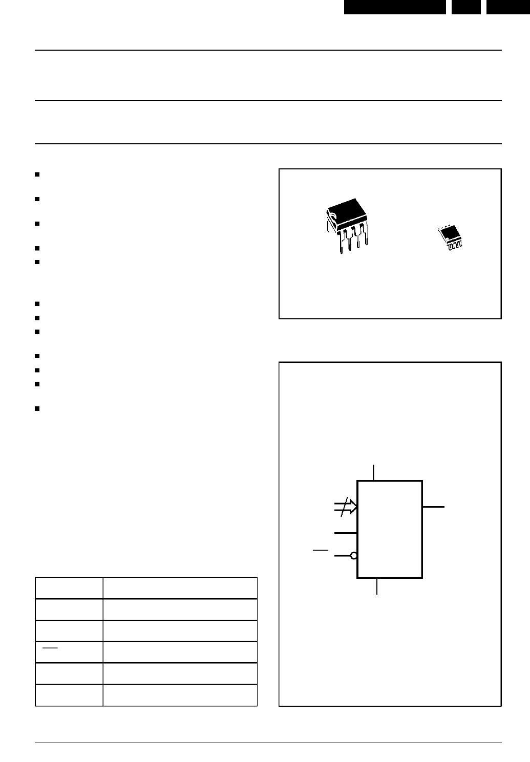
IC Descriptions. GB 83ASD-1 9.
ST24E32
ST25E32
32K SERIAL I2C EEPROM
with EXTENDED ADDRESSING
NOT FOR NEW DESIGN
AI01201B
3
E0-E2 SDA
VCC
ST24E32
ST25E32
WC
SCL
VSS
Figure 1. Logic Diagram
COMPATIBLE with I
2
C EXTENDED
ADDRESSING
TWO WIRE SERIAL INTERFACE,
SUPPORTS 400kHz PROTOCOL
1 MILLION ERASE/WRITE CYCLES, OVER
the FULL SUPPLY VOLTAGE RANGE
40 YEARS DATA RETENTION
SINGLE SUPPLY VOLTAGE
± 4.5V to 5.5V for ST24E32 version
± 2.5V to 5.5V for ST25E32 version
WRITE CONTROL FEATURE
BYTE and PAGE WRITE (up to 32 BYTES)
BYTE, RANDOM and SEQUENTIAL READ
MODES
SELF TIMED PROGRAMING CYCLE
AUTOMATIC ADDRESS INCREMENTING
ENHANCED ESD/LATCH UP
PERFORMANCES
ST24E32and ST25E32 are replaced by the
M24C32
DESCRIPTION
The ST24/25E32 are 32K bit electrically erasable
programmable memories (EEPROM), organized
as 8 blocks of 512 x 8 bits. The ST25E32 operates
with a power supply value as low as 2.5V. Both
PlasticDual-in-Line and PlasticSmallOutline pack-
ages are available.
E0 - E2 Chip Enable Inputs
SDA Serial Data Address Input/Output
SCL Serial Clock
WC Write Control
VCC Supply Voltage
VSS Ground
Table 1. Signal Names
8
1
SO8 (M)
200mil Width
8
1
PSDIP8 (B)
0.25mm Frame
IC Descriptions.
GB 84 ASD-19.
SDAVSS
SCL
WCE1
E0 VCC
E2
AI01202B
ST24E32
ST25E32
1
2
3
4
8
7
6
5
Figure 2A. DIP Pin Connections
1
AI01203C
2
3
4
8
7
6
5SDAVSS
SCL
WCE1
E0 VCC
E2
ST24E32
ST25E32
Figure 2B. SO Pin Connections
Each memory is compatible with the I
2
C extended
addressing standard, two wire serial interface
which uses a bi-directional data bus and serial
clock. The ST24/25E32carry a built-in 4 bit, unique
device identification code (1010) corresponding to
the I
2
C bus definition. The ST24/25E32 behave as
DESCRIPTION (cont'd) slave devices in the I
2
C protocol with all memory
operations synchronized by the serial clock. Read
and write operations are initiated by a START
conditiongeneratedby the bus master. The START
condition is followed by a stream of 4 bits(identifi-
cation code 1010), 3 bit Chip Enable input to form
a 7 bit Device Select, plus one read/write bit and
terminatedby an acknowledge bit.
Symbol Parameter Value Unit
T
A
Ambient Operating Temperature ±40 to 125 °C
T
STG
Storage Temperature ±65 to 150 °C
T
LEAD
Lead Temperature, Soldering (SO8)
(PSDIP8) 40 sec
10 sec 215
260 °C
V
IO
Input or Output Voltages ±0.6 to 6.5 V
V
CC
Supply Voltage ±0.3 to 6.5 V
V
ESD
Electrostatic Discharge Voltage (Human Body model)
(2)
4000 V
Electrostatic Discharge Voltage (Machine model)
(3)
500 V
Notes: 1. Except for the rating ºOperating Temperature Rangeº, stresses above those listed in the Table ºAbsolute Maximum Ratingsº
may cause permanent damage to the device. These are stress ratings only and operation of the device at these or any other
conditions above thoseindicated in the Operating sections of this specification is not implied. Exposure to Absolute Maximum
Rating conditions for extended periods may affect device reliability. Refer also to the SGS-THOMSON SURE Program and
other relevant quality documents.
2. 100pF through 1500Ω; MIL-STD-883C, 3015.7
3. 200pF through 0Ω; EIAJ IC-121 (condition C)
Table 2. Absolute Maximum Ratings
(1)
ST24E32, ST25E32

Spare parts list GB 85ASD-1 10.
10. Spare parts list
VAL6011
Various
0001 3139 197 60090 GENEVA LP LOADER
ASSY
0002 9305 022 60101 VAM6001/01
0003 3139 194 00710 SUSPENSION
0004 3139 194 00710 SUSPENSION
0005 3139 194 00620 SUSPENSION
0006 3139 194 00620 SUSPENSION
0007 3139 197 60060 CLAMPER ASSEMBLY
Loader
Various
0004 4822 358 10266
0009 3139 198 80010
0010 4822 532 13097 TULE
0011 3139 194 00270
0012 3139 197 50060
Monoboard
Various
1104 2422 025 15963 CON BM H 24P F 0.50 FFC
SMD R
1106 2422 025 16158 CON BM H 8P F 1.00 FFC
0.3 R
1205 2422 540 98428 RES CER SM 8M467
CSTCC8.46MHz R
1300 2422 540 98426 RES CER SM 6MHz
CSTCC6.00MHz R
1301 4822 267 51454 CONN. 11P FEMALE
1603 2422 025 16389 CON BM V 22P F 1.00 FFC
0.3 R
1604 2422 025 16388 CON BM V 16P F 1.00 FFC
0.3 R
g
2100 4822 126 14305 100nF 10% 16V 0603
2101 4822 126 14305 100nF 10% 16V 0603
2103 4822 124 80151 47µF 16V
2104 4822 126 13193 4.7nF 10% 63V
2105 4822 122 33761 22pF 5% 50V
2107 4822 126 13956 68pF 5% 63V CASE 0603
2108 4822 126 14315 390pF 5% 50V 0603
2109 2020 552 95697
2110 2222 861 15222 50V 2N2 PM5
2111 4822 126 14305 100nF 10% 16V 0603
2112 5322 126 11578 1nF 10% 50V 0603
2113 4822 126 14305 100nF 10% 16V 0603
2114 4822 122 31765 100pF 2% 63V
2115 4822 126 14305 100nF 10% 16V 0603
2116 4822 126 14305 100nF 10% 16V 0603
2117 4822 126 14305 100nF 10% 16V 0603
2120 4822 126 14305 100nF 10% 16V 0603
2121 4822 126 13879 220nF 20% 16V
2123 4822 126 14305 100nF 10% 16V 0603
2124 4822 126 14305 100nF 10% 16V 0603
2125 4822 126 14305 100nF 10% 16V 0603
2126 4822 126 14305 100nF 10% 16V 0603
2127 4822 126 14305 100nF 10% 16V 0603
2128 4822 126 14508 180pF 5% 50V 0603
2129 4822 126 14508 180pF 5% 50V 0603
2130 4822 122 33761 22pF 5% 50V
2131 4822 126 14494 22nF 10% 25V 0603
2136 4822 126 14305 100nF 10% 16V 0603
2137 4822 126 14305 100nF 10% 16V 0603
2138 4822 126 14305 100nF 10% 16V 0603
2139 4822 126 14305 100nF 10% 16V 0603
2140 4822 126 14241 0603 50V 330P COL R
2141 4822 122 33761 22pF 5% 50V
2142 5322 126 11583 10nF 10% 50V 0603
2143 4822 126 13883 220pF 5% 50V
2144 4822 126 13883 220pF 5% 50V
2145 4822 126 13883 220pF 5% 50V
2203 4822 126 14305 100nF 10% 16V 0603
2204 4822 126 14305 100nF 10% 16V 0603
2205 4822 126 14305 100nF 10% 16V 0603
2206 4822 126 14549 33nF 16V O6O3
2207 5322 126 11578 1nF 10% 50V 0603
2208 4822 126 14305 100nF 10% 16V 0603
2209 4822 126 14305 100nF 10% 16V 0603
2210 5322 126 11578 1nF 10% 50V 0603
2212 4822 126 14305 100nF 10% 16V 0603
2213 4822 126 14305 100nF 10% 16V 0603
2215 4822 124 23237 22µF 6.3V
2216 5322 126 11578 1nF 10% 50V 0603
2226 4822 126 14305 100nF 10% 16V 0603
2227 4822 126 14305 100nF 10% 16V 0603
2228 4822 126 14305 100nF 10% 16V 0603
2300 4822 126 14305 100nF 10% 16V 0603
2301 4822 126 14305 100nF 10% 16V 0603
2302 4822 126 14305 100nF 10% 16V 0603
2303 4822 124 80349 47µF 20% 6.3V
2306 4822 124 23002 10µF 16V
2309 4822 126 14305 100nF 10% 16V 0603
2310 4822 126 14305 100nF 10% 16V 0603
2314 4822 126 14305 100nF 10% 16V 0603
2315 4822 126 14305 100nF 10% 16V 0603
2318 5322 122 33861 120pF 10% 50V
2319 4822 126 11669 27pF
2401 4822 126 14305 100nF 10% 16V 0603
2402 4822 126 14305 100nF 10% 16V 0603
2403 4822 126 14305 100nF 10% 16V 0603
2404 4822 126 14305 100nF 10% 16V 0603
2405 4822 126 14305 100nF 10% 16V 0603
2406 4822 126 14305 100nF 10% 16V 0603
2407 4822 126 14305 100nF 10% 16V 0603
2408 4822 126 14305 100nF 10% 16V 0603
2409 4822 126 14305 100nF 10% 16V 0603
2410 4822 126 14305 100nF 10% 16V 0603
2411 4822 126 14305 100nF 10% 16V 0603
2412 4822 126 14305 100nF 10% 16V 0603
2413 4822 126 14305 100nF 10% 16V 0603
2418 4822 124 12095 100µF 20% 16V
2419 4822 124 80349 47µF 20% 6.3V
2420 4822 124 80349 47µF 20% 6.3V
2500 4822 126 14305 100nF 10% 16V 0603
2502 3198 030 74780 EL SM 35V 4U7 PM20 COL
R
2503 4822 126 14305 100nF 10% 16V 0603
2504 4822 122 31765 100pF 2% 63V
2505 4822 126 14494 22nF 10% 25V 0603
2506 4822 124 23002 10µF 16V
2507 4822 126 14305 100nF 10% 16V 0603
2508 5322 126 11579 3.3nF 10% 63V
2509 4822 126 14241 0603 50V 330P COL R
2510 4822 126 14305 100nF 10% 16V 0603
2511 4822 126 14305 100nF 10% 16V 0603
2512 4822 126 14305 100nF 10% 16V 0603
2513 4822 126 14305 100nF 10% 16V 0603
2514 4822 126 14305 100nF 10% 16V 0603
2515 4822 126 14305 100nF 10% 16V 0603
2516 4822 126 14305 100nF 10% 16V 0603
2517 4822 126 14305 100nF 10% 16V 0603
2518 4822 126 14305 100nF 10% 16V 0603
2519 4822 126 14305 100nF 10% 16V 0603
2520 4822 126 14305 100nF 10% 16V 0603
2521 4822 126 14305 100nF 10% 16V 0603
2522 4822 126 14305 100nF 10% 16V 0603
2523 4822 126 14305 100nF 10% 16V 0603
2524 4822 126 14305 100nF 10% 16V 0603
2525 4822 126 14305 100nF 10% 16V 0603
2526 4822 126 14305 100nF 10% 16V 0603
2527 4822 126 14305 100nF 10% 16V 0603
2528 4822 126 14305 100nF 10% 16V 0603
2529 4822 126 14305 100nF 10% 16V 0603
2530 3198 030 74780 EL SM 35V 4U7 PM20 COL
R
2531 3198 030 74780 EL SM 35V 4U7 PM20 COL
R
2532 4822 122 33777 47pF 5% 63V
2533 4822 122 33777 47pF 5% 63V
2534 5322 126 11578 1nF 10% 50V 0603
2535 5322 126 11578 1nF 10% 50V 0603
2600 4822 126 14494 22nF 10% 25V 0603
2601 4822 126 14247 0603 50V 1N5 COL R
2602 4822 126 14247 0603 50V 1N5 COL R
2603 4822 126 14305 100nF 10% 16V 0603
2604 4822 124 12095 100µF 20% 16V
2605 4822 126 14494 22nF 10% 25V 0603
2606 4822 124 12095 100µF 20% 16V
2607 4822 124 12095 100µF 20% 16V
2608 4822 124 23002 10µF 16V
2609 4822 124 80151 47µF 16V
2610 4822 126 14305 100nF 10% 16V 0603
2611 4822 124 12095 100µF 20% 16V
2614 4822 122 33777 47pF 5% 63V
2615 4822 122 33777 47pF 5% 63V
2616 4822 122 33777 47pF 5% 63V
2617 4822 122 33777 47pF 5% 63V
2618 4822 126 14305 100nF 10% 16V 0603
2619 4822 126 14305 100nF 10% 16V 0603
2620 4822 122 33777 47pF 5% 63V
2621 4822 122 33777 47pF 5% 63V
2622 4822 122 33777 47pF 5% 63V
2623 4822 122 33777 47pF 5% 63V
2624 4822 122 33777 47pF 5% 63V
2625 4822 122 33777 47pF 5% 63V
2626 4822 122 33777 47pF 5% 63V
2627 4822 122 33777 47pF 5% 63V
2632 4822 124 12095 100µF 20% 16V
2633 4822 124 12095 100µF 20% 16V
2634 4822 126 14305 100nF 10% 16V 0603
2635 4822 126 14305 100nF 10% 16V 0603
2636 4822 126 14305 100nF 10% 16V 0603
2637 4822 126 14305 100nF 10% 16V 0603
2638 4822 126 14305 100nF 10% 16V 0603
2639 4822 126 14305 100nF 10% 16V 0603
f
3100 4822 117 11152 4Ω7 5%
3102 5322 117 13034 1k5 1% 0.063W 0603
RC22H
3103 5322 117 13034 1k5 1% 0.063W 0603
RC22H
3104 5322 117 13062 390Ω 1% 0.063W 0603
RC22H
3105 4822 051 30103 10k 5% 0.062W
3106 4822 051 30479 47Ω 5% 0.062W
3107 4822 051 20228 2Ω2 5% 0.1W
3108 4822 051 20228 2Ω2 5% 0.1W
3110 4822 051 30479 47Ω 5% 0.062W
3111 5322 117 13058 150Ω 1% 0.063W 0603
RC22H
3112 5322 117 13021 47Ω 1% 0.063W 0603
RC22H
3114 4822 051 20228 2Ω2 5% 0.1W
3115 4822 051 20228 2Ω2 5% 0.1W
3116 5322 117 13042 3k9 1% 0.063W 0603
RC22H
3117 4822 051 30181 180Ω 5% 0.062W
3118 4822 051 30681 680Ω 5% 0.062W
3119 5322 117 13062 390Ω 1% 0.063W 0603
RC22H
3120 4822 051 30102 1k 5% 0.062W
3121 4822 051 30273 27k 5% 0.062W
3122 4822 051 30471 470Ω 5% 0.062W
3123 4822 051 30103 10k 5% 0.062W
3124 4822 051 30471 470Ω 5% 0.062W
3125 4822 051 30103 10k 5% 0.062W
3126 4822 051 30103 10k 5% 0.062W
3127 4822 051 30223 22k 5% 0.062W
3128 2322 704 69109
3129 4822 051 30392 3k9 5% 0.063W 0603
3130 4822 051 20228 2Ω2 5% 0.1W
3131 4822 051 20228 2Ω2 5% 0.1W
3132 4822 051 20228 2Ω2 5% 0.1W
3133 4822 051 20228 2Ω2 5% 0.1W
3134 5322 117 13047 330Ω 1% 0.063W 0603
RC22H
3135 4822 117 13613 2Ω2 5% 0603
3137 4822 117 13613 2Ω2 5% 0603
3138 5322 117 13053 6k8 1% 0.063W 0603
RC22H
3139 4822 117 12917 1Ω 5% 0.062W CASE0603
3140 4822 051 30479 47Ω 5% 0.062W
3141 4822 117 11152 4Ω7 5%
3142 5322 117 13028 12k 1% 0.063W 0603
RC22H
3143 5322 117 13043 220Ω 1% 0.063W 0603
RC22H
3144 2322 704 69109
3146 4822 051 30103 10k 5% 0.062W
3147 4822 051 30103 10k 5% 0.062W
3148 5322 117 13022 22k 1% 0.063W 0603
RC22H
3153 4822 117 12139 22Ω 5% 0.062W
3155 4822 051 30103 10k 5% 0.062W
3157 4822 051 30103 10k 5% 0.062W
3158 5322 117 13017 100Ω 1% 0.063W 0603
RC22H
3160 4822 051 30101 100Ω 5% 0.062W
3161 4822 117 13613 2Ω2 5% 0603
3162 4822 051 30101 100Ω 5% 0.062W
3163 4822 051 30273 27k 5% 0.062W
3164 4822 117 13613 2Ω2 5% 0603

Spare parts list
GB 86 ASD-110.
3165 5322 117 13063 120Ω 1% 0.063W 0603
RC22H
3166 4822 051 30393 39k 5% 0.062W
3167 4822 051 30101 100Ω 5% 0.062W
3168 5322 117 13047 330Ω 1% 0.063W 0603
RC22H
3169 4822 051 30101 100Ω 5% 0.062W
3170 4822 051 30101 100Ω 5% 0.062W
3171 4822 051 30101 100Ω 5% 0.062W
3172 4822 117 13632 100k 1% 0603 0.62W
3173 4822 117 13632 100k 1% 0603 0.62W
3174 4822 117 11152 4Ω7 5%
3175 4822 117 13613 2Ω2 5% 0603
3176 4822 051 30153 15k 5% 0.062W
3178 4822 117 11151 1Ω 5%
3179 4822 051 30221 220Ω 5% 0.062W
3180 4822 117 13632 100k 1% 0603 0.62W
3181 4822 051 30561 560Ω 5% 0.062W
3182 5322 117 13018 1k0 1% 0.063W 0603
RC22H
3183 5322 117 13017 100Ω 1% 0.063W 0603
RC22H
3184 2322 704 61204
3185 4822 117 11151 1Ω 5%
3187 4822 051 30273 27k 5% 0.062W
3189 4822 051 30008 0Ω jumper
3190 4822 051 30008 0Ω jumper
3191 4822 051 30008 0Ω jumper
3192 4822 051 30008 0Ω jumper
3193 4822 051 30008 0Ω jumper
3194 4822 051 30008 0Ω jumper
3195 4822 051 30008 0Ω jumper
3197 4822 051 30008 0Ω jumper
3198 5322 117 13049 470Ω 1% 0.063W 0603
RC22H
3199 5322 117 13042 3k9 1% 0.063W 0603
RC22H
3200 4822 051 30103 10k 5% 0.062W
3201 4822 117 11151 1Ω 5%
3202 4822 117 11151 1Ω 5%
3203 4822 051 30105 1M 5% 0.062W
3204 4822 051 30331 330Ω 5% 0.062W
3205 4822 051 30103 10k 5% 0.062W
3206 4822 051 30103 10k 5% 0.062W
3208 4822 051 30272 2k7 5% 0.062W
3209 4822 051 30472 4k7 5% 0.062W
3210 4822 051 30392 3k9 5% 0.063W 0603
3211 4822 051 30472 4k7 5% 0.062W
3212 4822 117 11152 4Ω7 5%
3213 4822 117 11152 4Ω7 5%
3214 4822 051 30392 3k9 5% 0.063W 0603
3215 4822 051 30103 10k 5% 0.062W
3219 4822 051 30103 10k 5% 0.062W
3220 4822 051 30103 10k 5% 0.062W
3221 4822 051 30103 10k 5% 0.062W
3224 4822 051 30151 150Ω 5% 0.062W
3225 2322 704 62004
3226 4822 051 30103 10k 5% 0.062W
3227 4822 051 30472 4k7 5% 0.062W
3229 4822 051 30123 12k 5% 0.062W
3230 4822 051 30103 10k 5% 0.062W
3231 4822 051 30103 10k 5% 0.062W
3232 4822 117 13613 2Ω2 5% 0603
3234 4822 117 12902 8k2 1% 0.063W 0603
3235 4822 117 13632 100k 1% 0603 0.62W
3236 4822 051 30472 4k7 5% 0.062W
3237 4822 051 30103 10k 5% 0.062W
3238 4822 051 30103 10k 5% 0.062W
3239 4822 051 30103 10k 5% 0.062W
3240 4822 051 30103 10k 5% 0.062W
3242 4822 051 30008 0Ω jumper
3243 4822 051 30008 0Ω jumper
3246 4822 051 30008 0Ω jumper
3247 4822 051 30008 0Ω jumper
3249 4822 051 30008 0Ω jumper
3250 4822 051 30008 0Ω jumper
3251 4822 051 30008 0Ω jumper
3252 4822 051 30008 0Ω jumper
3253 4822 051 30008 0Ω jumper
3254 4822 051 30008 0Ω jumper
3255 4822 051 30008 0Ω jumper
3256 4822 051 30008 0Ω jumper
3257 4822 051 30008 0Ω jumper
3258 4822 051 30008 0Ω jumper
3259 4822 117 11151 1Ω 5%
3260 4822 117 11151 1Ω 5%
3300 4822 117 11152 4Ω7 5%
3301 4822 051 30105 1M 5% 0.062W
3302 4822 051 30221 220Ω 5% 0.062W
3304 4822 051 30272 2k7 5% 0.062W
3305 4822 051 30272 2k7 5% 0.062W
3309 4822 051 30103 10k 5% 0.062W
3310 4822 051 30223 22k 5% 0.062W
3311 4822 051 30223 22k 5% 0.062W
3312 4822 051 30472 4k7 5% 0.062W
3313 4822 051 30472 4k7 5% 0.062W
3316 4822 051 20108 1Ω 5% 0.1W
3317 4822 051 20108 1Ω 5% 0.1W
3318 4822 051 30472 4k7 5% 0.062W
3319 4822 051 30479 47Ω 5% 0.062W
3320 4822 051 30472 4k7 5% 0.062W
3321 4822 051 30682 6k8 5% 0.062W
3322 5322 117 13026 4k7 1% 0.063W 0603
RC22H
3323 5322 117 13026 4k7 1% 0.063W 0603
RC22H
3324 4822 117 13632 100k 1% 0603 0.62W
3325 4822 051 30682 6k8 5% 0.062W
3326 4822 051 30479 47Ω 5% 0.062W
3327 4822 051 30682 6k8 5% 0.062W
3328 4822 051 30223 22k 5% 0.062W
3329 4822 051 30223 22k 5% 0.062W
3330 4822 051 30223 22k 5% 0.062W
3331 4822 051 30332 3k3 5% 0.062W
3332 4822 051 30332 3k3 5% 0.062W
3333 4822 051 30101 100Ω 5% 0.062W
3334 4822 051 30101 100Ω 5% 0.062W
3335 4822 051 30101 100Ω 5% 0.062W
3336 4822 051 30101 100Ω 5% 0.062W
3337 4822 051 30101 100Ω 5% 0.062W
3338 4822 051 30101 100Ω 5% 0.062W
3339 4822 051 30008 0Ω jumper
3340 4822 051 30008 0Ω jumper
3403 4822 051 30103 10k 5% 0.062W
3404 4822 051 30103 10k 5% 0.062W
3405 4822 051 30103 10k 5% 0.062W
3412 4822 051 30008 0Ω jumper
3414 4822 051 30008 0Ω jumper
3416 4822 051 30008 0Ω jumper
3500 4822 051 30332 3k3 5% 0.062W
3501 4822 051 30332 3k3 5% 0.062W
3502 4822 051 30223 22k 5% 0.062W
3503 4822 051 30103 10k 5% 0.062W
3504 4822 051 30103 10k 5% 0.062W
3505 4822 051 30103 10k 5% 0.062W
3506 4822 051 30103 10k 5% 0.062W
3507 4822 051 30472 4k7 5% 0.062W
3508 4822 051 30689 68Ω 5% 0.063W 0603
RC21 RST SM
3509 4822 051 30103 10k 5% 0.062W
3511 4822 051 30332 3k3 5% 0.062W
3512 4822 051 30332 3k3 5% 0.062W
3513 4822 051 30103 10k 5% 0.062W
3514 4822 051 30103 10k 5% 0.062W
3515 4822 051 30103 10k 5% 0.062W
3516 4822 051 30103 10k 5% 0.062W
3517 4822 051 30332 3k3 5% 0.062W
3519 4822 051 30103 10k 5% 0.062W
3520 4822 051 30103 10k 5% 0.062W
3521 4822 051 30103 10k 5% 0.062W
3522 4822 051 30103 10k 5% 0.062W
3523 4822 051 30332 3k3 5% 0.062W
3524 4822 051 30101 100Ω 5% 0.062W
3525 4822 051 30103 10k 5% 0.062W
3526 4822 051 30103 10k 5% 0.062W
3534 4822 051 30103 10k 5% 0.062W
3535 4822 051 30153 15k 5% 0.062W
3536 4822 051 30101 100Ω 5% 0.062W
3537 4822 051 30331 330Ω 5% 0.062W
3538 4822 051 30681 680Ω 5% 0.062W
3541 4822 051 30479 47Ω 5% 0.062W
3542 4822 051 30479 47Ω 5% 0.062W
3545 4822 051 30221 220Ω 5% 0.062W
3546 4822 051 30101 100Ω 5% 0.062W
3548 4822 051 30008 0Ω jumper
3549 4822 051 30008 0Ω jumper
3550 4822 051 30101 100Ω 5% 0.062W
3551 4822 051 30101 100Ω 5% 0.062W
3552 4822 051 30008 0Ω jumper
3554 4822 051 30008 0Ω jumper
3564 4822 051 30008 0Ω jumper
3566 4822 051 30008 0Ω jumper
3570 4822 051 30101 100Ω 5% 0.062W
3571 4822 051 30689 68Ω 5% 0.063W 0603
RC21 RST SM
3572 4822 051 30689 68Ω 5% 0.063W 0603
RC21 RST SM
3605 4822 051 30008 0Ω jumper
3606 4822 117 12925 47k 1% 0.063W 0603
3607 4822 117 13632 100k 1% 0603 0.62W
3608 4822 117 13632 100k 1% 0603 0.62W
3609 4822 117 13632 100k 1% 0603 0.62W
3610 4822 051 30103 10k 5% 0.062W
3611 4822 051 30103 10k 5% 0.062W
3612 4822 051 30103 10k 5% 0.062W
3613 4822 051 30103 10k 5% 0.062W
3614 4822 051 30103 10k 5% 0.062W
3615 4822 051 30103 10k 5% 0.062W
3616 4822 051 30103 10k 5% 0.062W
3618 4822 051 30223 22k 5% 0.062W
3619 4822 051 30223 22k 5% 0.062W
3620 4822 051 30101 100Ω 5% 0.062W
3621 4822 051 30101 100Ω 5% 0.062W
3622 4822 051 30101 100Ω 5% 0.062W
3623 4822 051 30101 100Ω 5% 0.062W
3624 4822 051 30101 100Ω 5% 0.062W
3625 4822 051 30101 100Ω 5% 0.062W
3626 4822 051 30102 1k 5% 0.062W
3627 4822 051 30471 470Ω 5% 0.062W
3628 4822 051 30471 470Ω 5% 0.062W
3629 4822 051 30472 4k7 5% 0.062W
3630 4822 051 30221 220Ω 5% 0.062W
3631 2322 704 64301 RST SM 0603 RC22H
430Ω PM1 R
3632 2322 704 64301 RST SM 0603 RC22H
430Ω PM1 R
3633 2322 704 64301 RST SM 0603 RC22H
430Ω PM1 R
3635 4822 051 30682 6k8 5% 0.062W
3636 4822 051 30682 6k8 5% 0.062W
3637 4822 051 30332 3k3 5% 0.062W
3642 4822 051 30103 10k 5% 0.062W
3647 2322 704 64301 RST SM 0603 RC22H
430Ω PM1 R
3648 2322 704 64301 RST SM 0603 RC22H
430Ω PM1 R
3651 2322 704 64301 RST SM 0603 RC22H
430Ω PM1 R
3654 2322 704 64301 RST SM 0603 RC22H
430Ω PM1 R
3655 2322 704 64301 RST SM 0603 RC22H
430Ω PM1 R
3656 2322 704 64301 RST SM 0603 RC22H
430Ω PM1 R
3657 2322 704 64301 RST SM 0603 RC22H
430Ω PM1 R
3658 4822 051 30102 1k 5% 0.062W
3659 4822 051 30102 1k 5% 0.062W
3660 4822 051 30102 1k 5% 0.062W
3661 2322 704 64301 RST SM 0603 RC22H
430Ω PM1 R
3662 4822 051 30102 1k 5% 0.062W
3663 4822 051 30102 1k 5% 0.062W
3664 2322 704 64301 RST SM 0603 RC22H
430Ω PM1 R
3665 4822 117 12139 22Ω 5% 0.062W
3667 4822 051 30331 330Ω 5% 0.062W
3669 4822 051 30008 0Ω jumper
3670 4822 051 30008 0Ω jumper
3671 4822 051 30223 22k 5% 0.062W
3672 4822 051 30479 47Ω 5% 0.062W
3673 4822 051 30101 100Ω 5% 0.062W
3677 4822 051 30008 0Ω jumper
3678 4822 051 30008 0Ω jumper
3679 4822 051 30008 0Ω jumper
3681 4822 051 30008 0Ω jumper
3683 4822 051 30008 0Ω jumper
3685 4822 051 30008 0Ω jumper
3686 4822 051 30223 22k 5% 0.062W
3687 4822 051 30223 22k 5% 0.062W
3688 4822 051 30472 4k7 5% 0.062W
3689 4822 051 30223 22k 5% 0.062W
b
5200 4822 157 11717 BLM31P500SPT
5300 4822 157 11717 BLM31P500SPT
5301 4822 157 11717 BLM31P500SPT
5402 4822 157 11499 BLM11P600SPT
5403 4822 157 11499 BLM11P600SPT
5501 4822 157 70299 2.2µH (NL322522T-2R2J)
5502 4822 157 70299 2.2µH (NL322522T-2R2J)
5503 4822 157 71206 BLM21A601SPT
5504 4822 157 71206 BLM21A601SPT
5600 4822 157 71206 BLM21A601SPT
5601 4822 157 11499 BLM11P600SPT
5602 4822 157 10547 15µH 5%
5603 4822 157 71206 BLM21A601SPT
5604 4822 157 10547 15µH 5%
5605 4822 157 10547 15µH 5%
5606 4822 157 10547 15µH 5%
5607 4822 157 10547 15µH 5%
5608 4822 157 10547 15µH 5%
5609 4822 157 11717 BLM31P500SPT
5610 4822 157 11717 BLM31P500SPT
d
6200 4822 130 11397 BAS316
6301 9322 128 69685 S1D

Spare parts list GB 87ASD-1 10.
6302 9322 128 69685 S1D
6303 9322 128 69685 S1D
6600 4822 130 11528 1PS76SB10
ce
7100 5322 130 42718 BFS20
7101 5322 130 42718 BFS20
7102 9352 637 37518
7103 4822 209 17229 BA5938FM
7104 4822 209 30095 LM833D
7105 4822 209 32073 MC34072D
7106 5322 130 42718 BFS20
7109 4822 209 15083 AN78M09
7110 5322 130 60803 BST72A
7111 5322 130 60159 BC846B
7112 5322 130 60159 BC846B
7113 5322 130 60159 BC846B
7114 5322 130 60159 BC846B
7115 4822 130 60373 BC856B
7116 5322 130 60159 BC846B
7201 9351 869 80118
7202 3104 123 95660
7203 4822 130 60373 BC856B
7207 9352 636 60557 SAA7399HL/M2A
7304 4822 209 16877 BA6856FP
7310 4822 209 15899 CY7C199-15C
7311 9352 622 13557 SAA7335HL
7312 4822 130 60373 BC856B
7315 5322 130 60159 BC846B
7401 9322 132 01668 AM29LV160B
7404 9322 144 59668 IC SM MT48LC1M16A1TG-
7S (MRN)R
7405 9322 144 59668 IC SM MT48LC1M16A1TG-
7S (MRN)R
7501 5322 130 60159 BC846B
7503 9322 151 16671 IC SM STI5505AVC (ST00)
Y
7504 4822 242 10838 27MHZ 120P FX0-31FT
7505 8204 056 05580 IC SM M24C32-
WMN6TNKSA
7600 5322 209 71568 PC74HCT14T
7604 5322 130 60159 BC846B
7605 4822 209 17398 LD1117DT33
7607 5322 130 60159 BC846B
7608 4822 130 60373 BC856B
7609 4822 130 60373 BC856B
7610 5322 130 60159 BC846B
7611 9352 456 80115
7612 5322 130 60159 BC846B
7613 5322 130 60159 BC846B
7614 5322 130 60159 BC846B
7615 5322 130 60159 BC846B
7616 4822 209 16062 MK2742-03S
7617 5322 130 60159 BC846B
7618 5322 130 60159 BC846B
7620 4822 130 60373 BC856B
7621 4822 130 42804 BC817-25
