20XX XX.cours.manual.HC11.anglais.sysnum
User Manual:
Open the PDF directly: View PDF ![]() .
.
Page Count: 512 [warning: Documents this large are best viewed by clicking the View PDF Link!]
- TABLE OF CONTENTS
- LIST OF FIGURES
- LIST OF TABLES
- SECTION 1 GENERAL DESCRIPTION
- SECTION 2 PINS AND CONNECTIONS
- 2.1 Packages And Pin Names
- 2.2 Pin Descriptions
- 2.2.1 Power-Supply Pins (VDD and VSS)
- 2.2.2 Mode Select Pins (MODB/VSTBY and MODA/LIR)
- 2.2.3 Crystal Oscillator and Clock Pins (EXTAL, XTAL, and E)
- 2.2.4 Crystal Oscillator Application Information
- 2.2.5 Reset Pin (RESET)
- 2.2.6 Interrupt Pins (XIRQ, IRQ)
- 2.2.7 A/D Reference and Port E Pins (VREFL, VREFH, PE[7:0])
- 2.2.8 Timer Port A Pins
- 2.2.9 Serial Port D Pins
- 2.2.10 Ports B and C, STRA, and STRB Pins
- 2.3 Termination of Unused Pins
- 2.4 Avoidance of Pin Damage
- 2.4.1 Zap and Latchup
- 2.4.2 Protective Interface Circuits
- 2.4.3 Internal Circuitry — Digital Input-Only Pin
- 2.4.4 Internal Circuitry — Analog Input-Only Pin
- 2.4.5 Internal Circuitry — Digital I/O Pin
- 2.4.6 Internal Circuitry — Input/Open-Drain-Output Pin
- 2.4.7 Internal Circuitry — Digital Output-Only Pin
- 2.4.8 Internal Circuitry — MODB/VSTBY Pin
- 2.4.9 Internal Circuitry — IRQ/VPPBULK Pin
- 2.5 Typical Single-Chip-Mode System Connections
- 2.6 Typical Expanded-Mode-System Connections
- 2.7 System Development and Debug Features
- SECTION 3 CONFIGURATION AND MODES OF OPERATION
- 3.1 Hardware Mode Selection
- 3.2 EEPROM-Based CONFIG Register
- 3.3 Protected Control Register Bits
- 3.4 Normal MCU Operating Modes
- 3.5 Special MCU Operating Modes
- 3.6 Test and Bootstrap Mode Applications
- SECTION 4 ON-CHIP MEMORY
- SECTION 5 RESETS AND INTERRUPTS
- 5.1 Initial Conditions Established During Reset
- 5.2 Causes Of Reset
- 5.3 Interrupt Process
- 5.4 Non-Maskable Interrupts
- 5.5 Maskable Interrupts
- 5.6 Interrupt Request
- 5.7 Interrupts from Internal Peripheral Subsystems
- SECTION 6 CENTRAL PROCESSING UNIT
- SECTION 7 PARALLEL INPUT/OUTPUT
- 7.1 Parallel I/O Overview
- 7.2 Parallel I/O Register And Control Bit Explanations
- 7.3 Detailed I/O Pin Descriptions
- 7.4 Handshake I/O Subsystem
- SECTION 8 SYNCHRONOUS SERIAL PERIPHERAL INTERFACE
- SECTION 9 ASYNCHRONOUS SERIAL COMMUNICATIONS INTERFACE
- SECTION 10 MAIN TIMER AND REAL-TIME INTERRUPT
- 10.1 General Description
- 10.2 Free-Running Counter and Prescaler
- 10.3 Input-Capture Functions
- 10.3.1 Programmable Options
- 10.3.2 Using Input Capture to Measure Period and Frequency
- 10.3.3 Using Input Capture to Measure Pulse Width
- 10.3.4 Measuring Very Short Time Periods
- 10.3.5 Measuring Long Time Periods with Input Capture and Overflow
- 10.3.6 Establishing a Relationship between Software and an Event
- 10.3.7 Other Uses for Input-Capture Pins
- 10.4 Output-Compare Functions
- 10.5 Timing Details For The Main Timer System
- 10.6 Listing of Timer Examples
- SECTION 11 PULSE ACCUMULATOR
- SECTION 12 ANALOG-TO-DIGITAL CONVERTER SYSTEM
- APPENDIX A INSTRUCTION SET DETAILS
- APPENDIX B BOOTLOADER LISTINGS
- INDEX

Order this document by
M68HC11RM/AD
Rev. 3.0
NON-DISCLOSURE AGREEMENT REQUIRED
M68HC11
Reference Manual
HC11
HC11
HC11

NON-DISCLOSURE AGREEMENT REQUIRED
Motorola reserves the right to make changes without further notice to
any products herein to improve reliability, function or design. Motorola
does not assume any liability arising out of the application or use of any
product or circuit described herein; neither does it convey any license
under its patent rights nor the rights of others. Motorola products are not
designed, intended, or authorized for use as components in systems
intended for surgical implant into the body, or other applications intended
to support or sustain life, or for any other application in which the failure
of the Motorola product could create a situation where personal injury or
death may occur. Should Buyer purchase or use Motorola products for
any such unintended or unauthorized application, Buyer shall indemnify
and hold Motorola and its officers, employees, subsidiaries, affiliates,
and distributors harmless against all claims, costs, damages, and
expenses, and reasonable attorney fees arising out of, directly or
indirectly, any claim of personal injury or death associated with such
unintended or unauthorized use, even if such claim alleges that Motorola
was negligent regarding the design or manufacture of the part.

TABLE OF CONTENTS
Paragraph
Number Page
Number
M68HC11 TABLE OF CONTENTS MOTOROLA
REFERENCE MANUAL iii
Section 1
GENERAL DESCRIPTION
1.1 General Description of the MC68HC11A8 . . . . . . . . . . . . . . . . . . . . . . . . . . . . . . . . . . . . . . 1-1
1.2 Programmer’s Model . . . . . . . . . . . . . . . . . . . . . . . . . . . . . . . . . . . . . . . . . . . . . . . . . . . . . . 1-2
1.3 Product Derivatives . . . . . . . . . . . . . . . . . . . . . . . . . . . . . . . . . . . . . . . . . . . . . . . . . . . . . . . 1-4
Section 2
PINS AND CONNECTIONS
2.1 Packages And Pin Names . . . . . . . . . . . . . . . . . . . . . . . . . . . . . . . . . . . . . . . . . . . . . . . . . . 2-1
2.1.1 MC68HC11A8 . . . . . . . . . . . . . . . . . . . . . . . . . . . . . . . . . . . . . . . . . . . . . . . . . . . . . . 2-1
2.1.2 MC68HC11D3/711D3. . . . . . . . . . . . . . . . . . . . . . . . . . . . . . . . . . . . . . . . . . . . . . . . . 2-2
2.1.3 MC68HC11E9/711E9 . . . . . . . . . . . . . . . . . . . . . . . . . . . . . . . . . . . . . . . . . . . . . . . . . 2-3
2.1.4 MC68HC811E2 . . . . . . . . . . . . . . . . . . . . . . . . . . . . . . . . . . . . . . . . . . . . . . . . . . . . . 2-4
2.1.5 MC68HC11F1. . . . . . . . . . . . . . . . . . . . . . . . . . . . . . . . . . . . . . . . . . . . . . . . . . . . . . . 2-5
2.1.6 MC68HC24 Port Replacement Unit . . . . . . . . . . . . . . . . . . . . . . . . . . . . . . . . . . . . . . 2-6
2.2 Pin Descriptions . . . . . . . . . . . . . . . . . . . . . . . . . . . . . . . . . . . . . . . . . . . . . . . . . . . . . . . . . . 2-7
2.2.1 Power-Supply Pins (VDD and VSS) . . . . . . . . . . . . . . . . . . . . . . . . . . . . . . . . . . . . . . . 2-7
2.2.2 Mode Select Pins (MODB/VSTBY and MODA/LIR) . . . . . . . . . . . . . . . . . . . . . . . . . . . 2-8
2.2.3 Crystal Oscillator and Clock Pins (EXTAL, XTAL, and E) . . . . . . . . . . . . . . . . . . . . 2-11
2.2.4 Crystal Oscillator Application Information. . . . . . . . . . . . . . . . . . . . . . . . . . . . . . . . . 2-15
2.2.4.1 Crystals for Parallel Resonance . . . . . . . . . . . . . . . . . . . . . . . . . . . . . . . . . . . . 2-15
2.2.4.2 Using Crystal Oscillator Outputs. . . . . . . . . . . . . . . . . . . . . . . . . . . . . . . . . . . . 2-15
2.2.4.3 Using External Oscillator . . . . . . . . . . . . . . . . . . . . . . . . . . . . . . . . . . . . . . . . . 2-15
2.2.4.4 AT-strip vs AT-cut Crystals. . . . . . . . . . . . . . . . . . . . . . . . . . . . . . . . . . . . . . . . 2-16
2.2.5 Reset Pin (RESET). . . . . . . . . . . . . . . . . . . . . . . . . . . . . . . . . . . . . . . . . . . . . . . . . . 2-16
2.2.6 Interrupt Pins (XIRQ, IRQ) . . . . . . . . . . . . . . . . . . . . . . . . . . . . . . . . . . . . . . . . . . . . 2-17
2.2.7 A/D Reference and Port E Pins (VREFL, VREFH, PE[7:0]). . . . . . . . . . . . . . . . . . . . . 2-18
2.2.8 Timer Port A Pins . . . . . . . . . . . . . . . . . . . . . . . . . . . . . . . . . . . . . . . . . . . . . . . . . . . 2-19
2.2.9 Serial Port D Pins . . . . . . . . . . . . . . . . . . . . . . . . . . . . . . . . . . . . . . . . . . . . . . . . . . . 2-19
2.2.10 Ports B and C, STRA, and STRB Pins . . . . . . . . . . . . . . . . . . . . . . . . . . . . . . . . . . 2-20
2.3 Termination of Unused Pins. . . . . . . . . . . . . . . . . . . . . . . . . . . . . . . . . . . . . . . . . . . . . . . . 2-21
2.4 Avoidance of Pin Damage . . . . . . . . . . . . . . . . . . . . . . . . . . . . . . . . . . . . . . . . . . . . . . . . . 2-23
2.4.1 Zap and Latchup. . . . . . . . . . . . . . . . . . . . . . . . . . . . . . . . . . . . . . . . . . . . . . . . . . . . 2-24
2.4.2 Protective Interface Circuits . . . . . . . . . . . . . . . . . . . . . . . . . . . . . . . . . . . . . . . . . . . 2-24
2.4.3 Internal Circuitry — Digital Input-Only Pin . . . . . . . . . . . . . . . . . . . . . . . . . . . . . . . . 2-25
2.4.4 Internal Circuitry — Analog Input-Only Pin. . . . . . . . . . . . . . . . . . . . . . . . . . . . . . . . 2-26
2.4.5 Internal Circuitry — Digital I/O Pin . . . . . . . . . . . . . . . . . . . . . . . . . . . . . . . . . . . . . . 2-28
2.4.6 Internal Circuitry — Input/Open-Drain-Output Pin . . . . . . . . . . . . . . . . . . . . . . . . . . 2-29
2.4.7 Internal Circuitry — Digital Output-Only Pin . . . . . . . . . . . . . . . . . . . . . . . . . . . . . . . 2-29
2.4.8 Internal Circuitry — MODB/VSTBY Pin . . . . . . . . . . . . . . . . . . . . . . . . . . . . . . . . . . 2-30
2.4.9 Internal Circuitry — IRQ/VPPBULK Pin. . . . . . . . . . . . . . . . . . . . . . . . . . . . . . . . . . . . 2-31
2.5 Typical Single-Chip-Mode System Connections . . . . . . . . . . . . . . . . . . . . . . . . . . . . . . . . 2-31
2.6 Typical Expanded-Mode-System Connections . . . . . . . . . . . . . . . . . . . . . . . . . . . . . . . . . 2-33
2.7 System Development and Debug Features . . . . . . . . . . . . . . . . . . . . . . . . . . . . . . . . . . . . 2-37
2.7.1 Load Instruction Register (LIR). . . . . . . . . . . . . . . . . . . . . . . . . . . . . . . . . . . . . . . . . 2-37
2.7.2 Internal Read Visibility (IRV). . . . . . . . . . . . . . . . . . . . . . . . . . . . . . . . . . . . . . . . . . . 2-37
2.7.3 MC68HC24 Port Replacement Unit . . . . . . . . . . . . . . . . . . . . . . . . . . . . . . . . . . . . . 2-38

Paragraph
Number Page
Number
MOTOROLA TABLE OF CONTENTS M68HC11
iv REFERENCE MANUAL
Section 3
CONFIGURATION AND MODES OF OPERATION
3.1 Hardware Mode Selection . . . . . . . . . . . . . . . . . . . . . . . . . . . . . . . . . . . . . . . . . . . . . . . . . . 3-1
3.1.1 Hardware Mode Select Pins . . . . . . . . . . . . . . . . . . . . . . . . . . . . . . . . . . . . . . . . . . . . 3-2
3.1.2 Mode Control Bits in the HPRIO Register . . . . . . . . . . . . . . . . . . . . . . . . . . . . . . . . . 3-2
3.2 EEPROM-Based CONFIG Register. . . . . . . . . . . . . . . . . . . . . . . . . . . . . . . . . . . . . . . . . . . 3-3
3.2.1 Operation of CONFIG Mechanism . . . . . . . . . . . . . . . . . . . . . . . . . . . . . . . . . . . . . . . 3-3
3.2.2 The CONFIG Register . . . . . . . . . . . . . . . . . . . . . . . . . . . . . . . . . . . . . . . . . . . . . . . . 3-4
3.3 Protected Control Register Bits . . . . . . . . . . . . . . . . . . . . . . . . . . . . . . . . . . . . . . . . . . . . . . 3-6
3.3.1 RAM and I/O Mapping Register (INIT) . . . . . . . . . . . . . . . . . . . . . . . . . . . . . . . . . . . . 3-6
3.3.2 Protected Control Bits in the TMSK2 Register . . . . . . . . . . . . . . . . . . . . . . . . . . . . . . 3-8
3.3.3 Protected Control Bits in the OPTION Register . . . . . . . . . . . . . . . . . . . . . . . . . . . . . 3-9
3.4 Normal MCU Operating Modes . . . . . . . . . . . . . . . . . . . . . . . . . . . . . . . . . . . . . . . . . . . . . 3-10
3.4.1 Normal Single-Chip Mode . . . . . . . . . . . . . . . . . . . . . . . . . . . . . . . . . . . . . . . . . . . . 3-10
3.4.2 Normal Expanded Mode. . . . . . . . . . . . . . . . . . . . . . . . . . . . . . . . . . . . . . . . . . . . . . 3-10
3.5 Special MCU Operating Modes . . . . . . . . . . . . . . . . . . . . . . . . . . . . . . . . . . . . . . . . . . . . . 3-11
3.5.1 Testing Functions Control Register (TEST1) . . . . . . . . . . . . . . . . . . . . . . . . . . . . . . 3-12
3.5.2 Test-Related Control Bits in the BAUD Register . . . . . . . . . . . . . . . . . . . . . . . . . . . 3-14
3.5.3 Special Test Mode . . . . . . . . . . . . . . . . . . . . . . . . . . . . . . . . . . . . . . . . . . . . . . . . . . 3-14
3.5.4 Special Bootstrap Mode . . . . . . . . . . . . . . . . . . . . . . . . . . . . . . . . . . . . . . . . . . . . . . 3-15
3.5.4.1 Loading Programs in Bootstrap Mode . . . . . . . . . . . . . . . . . . . . . . . . . . . . . . . 3-16
3.5.4.2 Executing User Programs in Bootstrap Mode . . . . . . . . . . . . . . . . . . . . . . . . . 3-16
3.5.4.3 Using Interrupts in Bootstrap Mode . . . . . . . . . . . . . . . . . . . . . . . . . . . . . . . . . 3-17
3.5.4.4 Bootloader Firmware Options. . . . . . . . . . . . . . . . . . . . . . . . . . . . . . . . . . . . . . 3-18
3.6 Test and Bootstrap Mode Applications . . . . . . . . . . . . . . . . . . . . . . . . . . . . . . . . . . . . . . . 3-19
Section 4
ON-CHIP MEMORY
4.1 ROM. . . . . . . . . . . . . . . . . . . . . . . . . . . . . . . . . . . . . . . . . . . . . . . . . . . . . . . . . . . . . . . . . . . 4-1
4.2 RAM . . . . . . . . . . . . . . . . . . . . . . . . . . . . . . . . . . . . . . . . . . . . . . . . . . . . . . . . . . . . . . . . . . . 4-2
4.2.1 Remapping Using the INIT Register. . . . . . . . . . . . . . . . . . . . . . . . . . . . . . . . . . . . . . 4-2
4.2.2 RAM Standby . . . . . . . . . . . . . . . . . . . . . . . . . . . . . . . . . . . . . . . . . . . . . . . . . . . . . . . 4-3
4.3 EEPROM . . . . . . . . . . . . . . . . . . . . . . . . . . . . . . . . . . . . . . . . . . . . . . . . . . . . . . . . . . . . . . . 4-4
4.3.1 Logical and Physical Organization . . . . . . . . . . . . . . . . . . . . . . . . . . . . . . . . . . . . . . . 4-4
4.3.2 Basic Operation of the EEPROM . . . . . . . . . . . . . . . . . . . . . . . . . . . . . . . . . . . . . . . . 4-5
4.3.3 Systems Operating below 2-MHz Bus Speed (E Clock). . . . . . . . . . . . . . . . . . . . . . . 4-9
4.3.4 EEPROM Programming Register (PPROG). . . . . . . . . . . . . . . . . . . . . . . . . . . . . . . 4-10
4.3.5 Programming/Erasing Procedures . . . . . . . . . . . . . . . . . . . . . . . . . . . . . . . . . . . . . . 4-12
4.3.5.1 Programming . . . . . . . . . . . . . . . . . . . . . . . . . . . . . . . . . . . . . . . . . . . . . . . . . . 4-12
4.3.5.2 Bulk Erase . . . . . . . . . . . . . . . . . . . . . . . . . . . . . . . . . . . . . . . . . . . . . . . . . . . . 4-12
4.3.5.3 Row Erase . . . . . . . . . . . . . . . . . . . . . . . . . . . . . . . . . . . . . . . . . . . . . . . . . . . . 4-13
4.3.5.4 Byte Erase . . . . . . . . . . . . . . . . . . . . . . . . . . . . . . . . . . . . . . . . . . . . . . . . . . . . 4-13
4.3.5.5 CONFIG Register . . . . . . . . . . . . . . . . . . . . . . . . . . . . . . . . . . . . . . . . . . . . . . . 4-13
4.3.6 Optional EEPROM Security Mode . . . . . . . . . . . . . . . . . . . . . . . . . . . . . . . . . . . . . . 4-14
4.4 EEPROM Application Information . . . . . . . . . . . . . . . . . . . . . . . . . . . . . . . . . . . . . . . . . . . 4-16
4.4.1 Conditions and Practices to Avoid . . . . . . . . . . . . . . . . . . . . . . . . . . . . . . . . . . . . . . 4-16
4.4.2 Using EEPROM to Select Product Options . . . . . . . . . . . . . . . . . . . . . . . . . . . . . . . 4-18
4.4.3 Using EEPROM for Setpoint and Calibration Information . . . . . . . . . . . . . . . . . . . . 4-18
4.4.4 Using EEPROM during Product Development . . . . . . . . . . . . . . . . . . . . . . . . . . . . . 4-19
4.4.5 Logging Data . . . . . . . . . . . . . . . . . . . . . . . . . . . . . . . . . . . . . . . . . . . . . . . . . . . . . . 4-19
4.4.6 Self-Adjusting Systems using EEPROM . . . . . . . . . . . . . . . . . . . . . . . . . . . . . . . . . 4-20
4.4.7 Software Methods to Extend Life Expectancy . . . . . . . . . . . . . . . . . . . . . . . . . . . . . 4-21

Paragraph
Number
Page
Number
M68HC11 TABLE OF CONTENTS MOTOROLA
REFERENCE MANUAL v
Section 5
RESETS AND INTERRUPTS
5.1 Initial Conditions Established During Reset . . . . . . . . . . . . . . . . . . . . . . . . . . . . . . . . . . . . . 5-1
5.1.1 System Initial Conditions . . . . . . . . . . . . . . . . . . . . . . . . . . . . . . . . . . . . . . . . . . . . . . 5-2
5.1.1.1 CPU . . . . . . . . . . . . . . . . . . . . . . . . . . . . . . . . . . . . . . . . . . . . . . . . . . . . . . . . . . 5-2
5.1.1.2 Memory Map. . . . . . . . . . . . . . . . . . . . . . . . . . . . . . . . . . . . . . . . . . . . . . . . . . . . 5-2
5.1.1.3 Parallel I/O . . . . . . . . . . . . . . . . . . . . . . . . . . . . . . . . . . . . . . . . . . . . . . . . . . . . . 5-2
5.1.1.4 Timer . . . . . . . . . . . . . . . . . . . . . . . . . . . . . . . . . . . . . . . . . . . . . . . . . . . . . . . . . 5-2
5.1.1.5 Real-Time Interrupt. . . . . . . . . . . . . . . . . . . . . . . . . . . . . . . . . . . . . . . . . . . . . . . 5-3
5.1.1.6 Pulse Accumulator . . . . . . . . . . . . . . . . . . . . . . . . . . . . . . . . . . . . . . . . . . . . . . . 5-3
5.1.1.7 COP Watchdog. . . . . . . . . . . . . . . . . . . . . . . . . . . . . . . . . . . . . . . . . . . . . . . . . . 5-3
5.1.1.8 Serial Communications Interface (SCI) . . . . . . . . . . . . . . . . . . . . . . . . . . . . . . . 5-3
5.1.1.9 Serial Peripheral Interface (SPI). . . . . . . . . . . . . . . . . . . . . . . . . . . . . . . . . . . . . 5-3
5.1.1.10 Analog-to-Digital (A/D) Converter. . . . . . . . . . . . . . . . . . . . . . . . . . . . . . . . . . . 5-3
5.1.1.11 Other System Controls . . . . . . . . . . . . . . . . . . . . . . . . . . . . . . . . . . . . . . . . . . . 5-4
5.1.2 CONFIG Register Allows Flexible Configuration . . . . . . . . . . . . . . . . . . . . . . . . . . . . 5-4
5.1.3 Mode of Operation Established . . . . . . . . . . . . . . . . . . . . . . . . . . . . . . . . . . . . . . . . . 5-5
5.1.4 Program Counter Loaded with Reset Vector . . . . . . . . . . . . . . . . . . . . . . . . . . . . . . . 5-5
5.2 Causes Of Reset . . . . . . . . . . . . . . . . . . . . . . . . . . . . . . . . . . . . . . . . . . . . . . . . . . . . . . . . . 5-5
5.2.1 Power-On Reset (POR) . . . . . . . . . . . . . . . . . . . . . . . . . . . . . . . . . . . . . . . . . . . . . . . 5-7
5.2.2 COP Watchdog Timer Reset . . . . . . . . . . . . . . . . . . . . . . . . . . . . . . . . . . . . . . . . . . . 5-7
5.2.3 Clock Monitor Reset . . . . . . . . . . . . . . . . . . . . . . . . . . . . . . . . . . . . . . . . . . . . . . . . . . 5-9
5.2.4 External Reset . . . . . . . . . . . . . . . . . . . . . . . . . . . . . . . . . . . . . . . . . . . . . . . . . . . . . 5-10
5.3 Interrupt Process . . . . . . . . . . . . . . . . . . . . . . . . . . . . . . . . . . . . . . . . . . . . . . . . . . . . . . . . 5-11
5.3.1 Interrupt Recognition and Stacking Registers . . . . . . . . . . . . . . . . . . . . . . . . . . . . . 5-12
5.3.2 Selecting Interrupt Vectors . . . . . . . . . . . . . . . . . . . . . . . . . . . . . . . . . . . . . . . . . . . . 5-12
5.3.3 Return from Interrupt . . . . . . . . . . . . . . . . . . . . . . . . . . . . . . . . . . . . . . . . . . . . . . . . 5-20
5.4 Non-Maskable Interrupts . . . . . . . . . . . . . . . . . . . . . . . . . . . . . . . . . . . . . . . . . . . . . . . . . . 5-20
5.4.1 Non-Maskable Interrupt Request (XIRQ) . . . . . . . . . . . . . . . . . . . . . . . . . . . . . . . . . 5-21
5.4.2 Illegal Opcode Fetch. . . . . . . . . . . . . . . . . . . . . . . . . . . . . . . . . . . . . . . . . . . . . . . . . 5-22
5.4.3 Software Interrupt . . . . . . . . . . . . . . . . . . . . . . . . . . . . . . . . . . . . . . . . . . . . . . . . . . . 5-23
5.5 Maskable Interrupts . . . . . . . . . . . . . . . . . . . . . . . . . . . . . . . . . . . . . . . . . . . . . . . . . . . . . . 5-23
5.5.1 I Bit in the Condition Code Register . . . . . . . . . . . . . . . . . . . . . . . . . . . . . . . . . . . . . 5-23
5.5.2 Special Considerations for I-Bit-Related Instructions . . . . . . . . . . . . . . . . . . . . . . . . 5-24
5.6 Interrupt Request . . . . . . . . . . . . . . . . . . . . . . . . . . . . . . . . . . . . . . . . . . . . . . . . . . . . . . . . 5-25
5.6.1 Selecting Edge Triggering or Level Triggering . . . . . . . . . . . . . . . . . . . . . . . . . . . . . 5-25
5.6.2 Sharing Vector with Handshake I/O Interrupts . . . . . . . . . . . . . . . . . . . . . . . . . . . . . 5-26
5.7 Interrupts from Internal Peripheral Subsystems. . . . . . . . . . . . . . . . . . . . . . . . . . . . . . . . . 5-26
5.7.1 Inhibiting Individual Sources. . . . . . . . . . . . . . . . . . . . . . . . . . . . . . . . . . . . . . . . . . . 5-27
5.7.2 Clearing Interrupt Status Flag Bits . . . . . . . . . . . . . . . . . . . . . . . . . . . . . . . . . . . . . . 5-27
5.7.3 Automatic Clearing Mechanisms on Some Flags. . . . . . . . . . . . . . . . . . . . . . . . . . . 5-27
Section 6
CENTRAL PROCESSING UNIT
6.1 Programmer’s Model . . . . . . . . . . . . . . . . . . . . . . . . . . . . . . . . . . . . . . . . . . . . . . . . . . . . . . 6-1
6.1.1 Accumulators (A, B, and D) . . . . . . . . . . . . . . . . . . . . . . . . . . . . . . . . . . . . . . . . . . . . 6-1
6.1.2 Index Registers (X and Y) . . . . . . . . . . . . . . . . . . . . . . . . . . . . . . . . . . . . . . . . . . . . . 6-2
6.1.3 Stack Pointer (SP) . . . . . . . . . . . . . . . . . . . . . . . . . . . . . . . . . . . . . . . . . . . . . . . . . . . 6-3
6.1.4 Program Counter (PC) . . . . . . . . . . . . . . . . . . . . . . . . . . . . . . . . . . . . . . . . . . . . . . . . 6-4
6.1.5 Condition Code Register (CCR) . . . . . . . . . . . . . . . . . . . . . . . . . . . . . . . . . . . . . . . . . 6-4
6.2 Addressing Modes . . . . . . . . . . . . . . . . . . . . . . . . . . . . . . . . . . . . . . . . . . . . . . . . . . . . . . . . 6-6
6.2.1 Immediate (IMM) . . . . . . . . . . . . . . . . . . . . . . . . . . . . . . . . . . . . . . . . . . . . . . . . . . . . 6-6

Paragraph
Number Page
Number
MOTOROLA TABLE OF CONTENTS M68HC11
vi REFERENCE MANUAL
6.2.2 Extended (EXT) . . . . . . . . . . . . . . . . . . . . . . . . . . . . . . . . . . . . . . . . . . . . . . . . . . . . . 6-7
6.2.3 Direct (DIR). . . . . . . . . . . . . . . . . . . . . . . . . . . . . . . . . . . . . . . . . . . . . . . . . . . . . . . . . 6-8
6.2.4 Indexed (INDX, INDY) . . . . . . . . . . . . . . . . . . . . . . . . . . . . . . . . . . . . . . . . . . . . . . . . 6-9
6.2.5 Inherent (INH). . . . . . . . . . . . . . . . . . . . . . . . . . . . . . . . . . . . . . . . . . . . . . . . . . . . . . 6-10
6.2.6 Relative (REL) . . . . . . . . . . . . . . . . . . . . . . . . . . . . . . . . . . . . . . . . . . . . . . . . . . . . . 6-10
6.3 M68HC11 Instruction Set. . . . . . . . . . . . . . . . . . . . . . . . . . . . . . . . . . . . . . . . . . . . . . . . . . 6-11
6.3.1 Accumulator and Memory Instructions . . . . . . . . . . . . . . . . . . . . . . . . . . . . . . . . . . . 6-11
6.3.1.1 Loads, Stores, And Transfers. . . . . . . . . . . . . . . . . . . . . . . . . . . . . . . . . . . . . . 6-11
6.3.1.2 Arithmetic Operations. . . . . . . . . . . . . . . . . . . . . . . . . . . . . . . . . . . . . . . . . . . . 6-12
6.3.1.3 Multiply and Divide . . . . . . . . . . . . . . . . . . . . . . . . . . . . . . . . . . . . . . . . . . . . . . 6-13
6.3.1.4 Logical Operations . . . . . . . . . . . . . . . . . . . . . . . . . . . . . . . . . . . . . . . . . . . . . . 6-14
6.3.1.5 Data Testing and Bit Manipulation . . . . . . . . . . . . . . . . . . . . . . . . . . . . . . . . . . 6-14
6.3.1.6 Shifts and Rotates . . . . . . . . . . . . . . . . . . . . . . . . . . . . . . . . . . . . . . . . . . . . . . 6-14
6.3.2 Stack and Index Register Instructions . . . . . . . . . . . . . . . . . . . . . . . . . . . . . . . . . . . 6-15
6.3.3 Condition Code Register Instructions . . . . . . . . . . . . . . . . . . . . . . . . . . . . . . . . . . . . 6-17
6.3.4 Program Control Instructions . . . . . . . . . . . . . . . . . . . . . . . . . . . . . . . . . . . . . . . . . . 6-17
6.3.4.1 Branches . . . . . . . . . . . . . . . . . . . . . . . . . . . . . . . . . . . . . . . . . . . . . . . . . . . . . 6-18
6.3.4.2 Jumps. . . . . . . . . . . . . . . . . . . . . . . . . . . . . . . . . . . . . . . . . . . . . . . . . . . . . . . . 6-19
6.3.4.3 Subroutine Calls And Returns (BSR, JSR, RTS) . . . . . . . . . . . . . . . . . . . . . . . 6-19
6.3.4.4 Interrupt Handling (RTI, SWI, WAI) . . . . . . . . . . . . . . . . . . . . . . . . . . . . . . . . . 6-19
6.3.4.5 Miscellaneous (NOP, STOP, TEST). . . . . . . . . . . . . . . . . . . . . . . . . . . . . . . . . 6-19
Section 7
PARALLEL INPUT/OUTPUT
7.1 Parallel I/O Overview . . . . . . . . . . . . . . . . . . . . . . . . . . . . . . . . . . . . . . . . . . . . . . . . . . . . . . 7-1
7.2 Parallel I/O Register And Control Bit Explanations . . . . . . . . . . . . . . . . . . . . . . . . . . . . . . . 7-3
7.2.1 Port Registers. . . . . . . . . . . . . . . . . . . . . . . . . . . . . . . . . . . . . . . . . . . . . . . . . . . . . . . 7-4
7.2.2 Data Direction Registers. . . . . . . . . . . . . . . . . . . . . . . . . . . . . . . . . . . . . . . . . . . . . . . 7-5
7.3 Detailed I/O Pin Descriptions . . . . . . . . . . . . . . . . . . . . . . . . . . . . . . . . . . . . . . . . . . . . . . . . 7-6
7.3.1 Port A . . . . . . . . . . . . . . . . . . . . . . . . . . . . . . . . . . . . . . . . . . . . . . . . . . . . . . . . . . . . . 7-7
7.3.1.1 PA[2:0] (IC[3:1]) Pin Logic . . . . . . . . . . . . . . . . . . . . . . . . . . . . . . . . . . . . . . . . . 7-7
7.3.1.2 PA[6:3] (OC[5:2]) Pin Logic . . . . . . . . . . . . . . . . . . . . . . . . . . . . . . . . . . . . . . . . 7-7
7.3.1.3 PA7 (OC1, PAI) Pin Logic . . . . . . . . . . . . . . . . . . . . . . . . . . . . . . . . . . . . . . . . . 7-8
7.3.1.4 Port A Idealized Timing . . . . . . . . . . . . . . . . . . . . . . . . . . . . . . . . . . . . . . . . . . 7-11
7.3.2 Port B . . . . . . . . . . . . . . . . . . . . . . . . . . . . . . . . . . . . . . . . . . . . . . . . . . . . . . . . . . . . 7-11
7.3.2.1 Port B Pin Logic . . . . . . . . . . . . . . . . . . . . . . . . . . . . . . . . . . . . . . . . . . . . . . . . 7-12
7.3.2.2 Port B Idealized Timing . . . . . . . . . . . . . . . . . . . . . . . . . . . . . . . . . . . . . . . . . . 7-13
7.3.2.3 Special Considerations For Port B On MC68HC24 PRU . . . . . . . . . . . . . . . . . 7-13
7.3.3 R/W (STRB) Pin . . . . . . . . . . . . . . . . . . . . . . . . . . . . . . . . . . . . . . . . . . . . . . . . . . . . 7-14
7.3.3.1 R/W (STRB) Pin Logic . . . . . . . . . . . . . . . . . . . . . . . . . . . . . . . . . . . . . . . . . . . 7-14
7.3.3.2 Special Considerations for STRB on MC68HC24 PRU . . . . . . . . . . . . . . . . . . 7-16
7.3.4 Port C . . . . . . . . . . . . . . . . . . . . . . . . . . . . . . . . . . . . . . . . . . . . . . . . . . . . . . . . . . . . 7-16
7.3.4.1 Port C Pin Logic for Expanded Modes . . . . . . . . . . . . . . . . . . . . . . . . . . . . . . . 7-16
7.3.4.2 Summary of Port C Idealized Expanded-Mode Timing . . . . . . . . . . . . . . . . . . 7-17
7.3.4.3 Port C Single-Chip Mode Pin Logic . . . . . . . . . . . . . . . . . . . . . . . . . . . . . . . . . 7-18
7.3.4.4 Port C Idealized Single-Chip Mode Timing. . . . . . . . . . . . . . . . . . . . . . . . . . . . 7-21
7.3.4.5 Special Considerations for Port C on MC68HC24 PRU. . . . . . . . . . . . . . . . . . 7-23
7.3.5 AS (STRA) Pin . . . . . . . . . . . . . . . . . . . . . . . . . . . . . . . . . . . . . . . . . . . . . . . . . . . . . 7-23
7.3.5.1 AS (STRA) Pin Logic . . . . . . . . . . . . . . . . . . . . . . . . . . . . . . . . . . . . . . . . . . . . 7-23
7.3.5.2 Special Considerations for STRA on MC68HC24 PRU . . . . . . . . . . . . . . . . . . 7-25
7.3.6 Port D . . . . . . . . . . . . . . . . . . . . . . . . . . . . . . . . . . . . . . . . . . . . . . . . . . . . . . . . . . . . 7-25
7.3.6.1 PD0 (RxD) Pin Logic . . . . . . . . . . . . . . . . . . . . . . . . . . . . . . . . . . . . . . . . . . . . 7-25

Paragraph
Number
Page
Number
M68HC11 TABLE OF CONTENTS MOTOROLA
REFERENCE MANUAL vii
7.3.6.2 PD1 (TxD) Pin Logic. . . . . . . . . . . . . . . . . . . . . . . . . . . . . . . . . . . . . . . . . . . . . 7-27
7.3.6.3 PD2 (MISO) Pin Logic . . . . . . . . . . . . . . . . . . . . . . . . . . . . . . . . . . . . . . . . . . . 7-29
7.3.6.4 PD3 (MOSI) Pin Logic . . . . . . . . . . . . . . . . . . . . . . . . . . . . . . . . . . . . . . . . . . . 7-31
7.3.6.5 PD4 (SCK) Pin Logic . . . . . . . . . . . . . . . . . . . . . . . . . . . . . . . . . . . . . . . . . . . . 7-33
7.3.6.6 PD5 (SS) Pin Logic. . . . . . . . . . . . . . . . . . . . . . . . . . . . . . . . . . . . . . . . . . . . . . 7-35
7.3.6.7 Idealized Port D Timing . . . . . . . . . . . . . . . . . . . . . . . . . . . . . . . . . . . . . . . . . . 7-37
7.3.7 Port E . . . . . . . . . . . . . . . . . . . . . . . . . . . . . . . . . . . . . . . . . . . . . . . . . . . . . . . . . . . . 7-39
7.3.7.1 Port E Pin Logic . . . . . . . . . . . . . . . . . . . . . . . . . . . . . . . . . . . . . . . . . . . . . . . . 7-39
7.3.7.2 Idealized Port E Timing . . . . . . . . . . . . . . . . . . . . . . . . . . . . . . . . . . . . . . . . . . 7-40
7.4 Handshake I/O Subsystem . . . . . . . . . . . . . . . . . . . . . . . . . . . . . . . . . . . . . . . . . . . . . . . . 7-41
7.4.1 Simple Strobe Mode . . . . . . . . . . . . . . . . . . . . . . . . . . . . . . . . . . . . . . . . . . . . . . . . . 7-42
7.4.1.1 Port B Strobe Output. . . . . . . . . . . . . . . . . . . . . . . . . . . . . . . . . . . . . . . . . . . . . 7-42
7.4.1.2 Port C Simple Latching Input . . . . . . . . . . . . . . . . . . . . . . . . . . . . . . . . . . . . . . 7-43
7.4.2 Full-input Handshake Mode . . . . . . . . . . . . . . . . . . . . . . . . . . . . . . . . . . . . . . . . . . . 7-43
7.4.3 Full-Output Handshake Mode. . . . . . . . . . . . . . . . . . . . . . . . . . . . . . . . . . . . . . . . . . 7-44
7.4.3.1 Normal Output Handshake. . . . . . . . . . . . . . . . . . . . . . . . . . . . . . . . . . . . . . . . 7-45
7.4.3.2 Three-State Variation of Output Handshake . . . . . . . . . . . . . . . . . . . . . . . . . . 7-45
7.4.4 Parallel I/O Control Register (PIOC). . . . . . . . . . . . . . . . . . . . . . . . . . . . . . . . . . . . . 7-46
7.4.5 Non-Handshake Uses of STRA and STRB Pins . . . . . . . . . . . . . . . . . . . . . . . . . . . 7-48
Section 8
SYNCHRONOUS SERIAL PERIPHERAL INTERFACE
8.1 SPI Transfer Formats. . . . . . . . . . . . . . . . . . . . . . . . . . . . . . . . . . . . . . . . . . . . . . . . . . . . . . 8-1
8.1.1 SPI Clock Phase and Polarity Controls . . . . . . . . . . . . . . . . . . . . . . . . . . . . . . . . . . . 8-1
8.1.2 CPHA Equals Zero Transfer Format . . . . . . . . . . . . . . . . . . . . . . . . . . . . . . . . . . . . . 8-2
8.1.3 CPHA Equals One Transfer Format . . . . . . . . . . . . . . . . . . . . . . . . . . . . . . . . . . . . . . 8-2
8.2 SPI Block Diagram. . . . . . . . . . . . . . . . . . . . . . . . . . . . . . . . . . . . . . . . . . . . . . . . . . . . . . . . 8-3
8.3 SPI Pin Signals . . . . . . . . . . . . . . . . . . . . . . . . . . . . . . . . . . . . . . . . . . . . . . . . . . . . . . . . . . 8-4
8.4 SPI Registers . . . . . . . . . . . . . . . . . . . . . . . . . . . . . . . . . . . . . . . . . . . . . . . . . . . . . . . . . . . . 8-6
8.4.1 Port D Data Direction Control Register (DDRD). . . . . . . . . . . . . . . . . . . . . . . . . . . . . 8-6
8.4.2 SPI Control Register (SPCR) . . . . . . . . . . . . . . . . . . . . . . . . . . . . . . . . . . . . . . . . . . . 8-7
8.4.3 SPI Status Register (SPSR) . . . . . . . . . . . . . . . . . . . . . . . . . . . . . . . . . . . . . . . . . . . . 8-8
8.5 SPI System Errors . . . . . . . . . . . . . . . . . . . . . . . . . . . . . . . . . . . . . . . . . . . . . . . . . . . . . . . . 8-9
8.5.1 SPI Mode-Fault Error . . . . . . . . . . . . . . . . . . . . . . . . . . . . . . . . . . . . . . . . . . . . . . . . . 8-9
8.5.2 SPI Write-Collision Errors. . . . . . . . . . . . . . . . . . . . . . . . . . . . . . . . . . . . . . . . . . . . . 8-10
8.6 Beginning and Ending SPI Transfers. . . . . . . . . . . . . . . . . . . . . . . . . . . . . . . . . . . . . . . . . 8-10
8.6.1 Transfer Beginning Period (Initiation Delay). . . . . . . . . . . . . . . . . . . . . . . . . . . . . . . 8-11
8.6.2 Transfer Ending Period. . . . . . . . . . . . . . . . . . . . . . . . . . . . . . . . . . . . . . . . . . . . . . . 8-12
8.7 Transfers to Peripherals with Odd Word Lengths . . . . . . . . . . . . . . . . . . . . . . . . . . . . . . . 8-14
8.7.1 Example 8–1: On-Chip SPI Driving an MC144110 D/A . . . . . . . . . . . . . . . . . . . . . . 8-16
8.7.2 Example 8–2: Software SPI Driving an MC144110 D/A. . . . . . . . . . . . . . . . . . . . . . 8-16
Section 9
ASYNCHRONOUS SERIAL COMMUNICATIONS INTERFACE
9.1 General Description . . . . . . . . . . . . . . . . . . . . . . . . . . . . . . . . . . . . . . . . . . . . . . . . . . . . . . . 9-1
9.1.1 Transmitter Block Diagram . . . . . . . . . . . . . . . . . . . . . . . . . . . . . . . . . . . . . . . . . . . . . 9-1
9.1.2 Receiver Block Diagram . . . . . . . . . . . . . . . . . . . . . . . . . . . . . . . . . . . . . . . . . . . . . . . 9-3
9.2 SCI Registers and Control Bits . . . . . . . . . . . . . . . . . . . . . . . . . . . . . . . . . . . . . . . . . . . . . . 9-5
9.2.1 Port D Related Registers and Control Bits (PORTD, DDRD, SPCR). . . . . . . . . . . . . 9-6
9.2.2 Baud-Rate Control Register (BAUD) . . . . . . . . . . . . . . . . . . . . . . . . . . . . . . . . . . . . . 9-7
9.2.3 SCI Control Register 1 (SCCR1) . . . . . . . . . . . . . . . . . . . . . . . . . . . . . . . . . . . . . . . . 9-9
9.2.4 SCI Control Register 2 (SCCR2) . . . . . . . . . . . . . . . . . . . . . . . . . . . . . . . . . . . . . . . 9-10

Paragraph
Number Page
Number
MOTOROLA TABLE OF CONTENTS M68HC11
viii REFERENCE MANUAL
9.2.5 SCI Status Register (SCSR). . . . . . . . . . . . . . . . . . . . . . . . . . . . . . . . . . . . . . . . . . . 9-11
9.2.6 SCI Data Register (SCDR) . . . . . . . . . . . . . . . . . . . . . . . . . . . . . . . . . . . . . . . . . . . . 9-14
9.3 SCI Transmitter . . . . . . . . . . . . . . . . . . . . . . . . . . . . . . . . . . . . . . . . . . . . . . . . . . . . . . . . . 9-14
9.3.1 Eight- and Nine-Bit Data Modes . . . . . . . . . . . . . . . . . . . . . . . . . . . . . . . . . . . . . . . . 9-15
9.3.2 Interrupts and Status Flags . . . . . . . . . . . . . . . . . . . . . . . . . . . . . . . . . . . . . . . . . . . 9-16
9.3.3 Send Break. . . . . . . . . . . . . . . . . . . . . . . . . . . . . . . . . . . . . . . . . . . . . . . . . . . . . . . . 9-16
9.3.4 Queued Idle Character . . . . . . . . . . . . . . . . . . . . . . . . . . . . . . . . . . . . . . . . . . . . . . . 9-17
9.3.5 Disabling the SCI Transmitter. . . . . . . . . . . . . . . . . . . . . . . . . . . . . . . . . . . . . . . . . . 9-18
9.3.6 TxD Pin Buffer Logic. . . . . . . . . . . . . . . . . . . . . . . . . . . . . . . . . . . . . . . . . . . . . . . . . 9-18
9.4 SCI Receiver . . . . . . . . . . . . . . . . . . . . . . . . . . . . . . . . . . . . . . . . . . . . . . . . . . . . . . . . . . . 9-20
9.4.1 Data Sampling Technique . . . . . . . . . . . . . . . . . . . . . . . . . . . . . . . . . . . . . . . . . . . . 9-20
9.4.2 Worst-Case Baud-Rate Mismatch . . . . . . . . . . . . . . . . . . . . . . . . . . . . . . . . . . . . . . 9-26
9.4.3 Double-Buffered Operation. . . . . . . . . . . . . . . . . . . . . . . . . . . . . . . . . . . . . . . . . . . . 9-28
9.4.4 Receive Status Flags and Interrupts . . . . . . . . . . . . . . . . . . . . . . . . . . . . . . . . . . . . 9-28
9.4.5 Receiver Wake-Up Operation. . . . . . . . . . . . . . . . . . . . . . . . . . . . . . . . . . . . . . . . . . 9-29
9.5 Baud-Rate Generator. . . . . . . . . . . . . . . . . . . . . . . . . . . . . . . . . . . . . . . . . . . . . . . . . . . . . 9-30
9.5.1 Timing Chain Block Diagram . . . . . . . . . . . . . . . . . . . . . . . . . . . . . . . . . . . . . . . . . . 9-30
9.5.2 Baud Rates vs. Crystal Frequency . . . . . . . . . . . . . . . . . . . . . . . . . . . . . . . . . . . . . . 9-30
9.6 SCI Timing Details . . . . . . . . . . . . . . . . . . . . . . . . . . . . . . . . . . . . . . . . . . . . . . . . . . . . . . . 9-30
9.6.1 Operation As Transmitter Is Enabled . . . . . . . . . . . . . . . . . . . . . . . . . . . . . . . . . . . . 9-31
9.6.2 TDRE and Transfers from SCDR to Transmit Shift Register . . . . . . . . . . . . . . . . . . 9-33
9.6.3 TC vs. Character Completion . . . . . . . . . . . . . . . . . . . . . . . . . . . . . . . . . . . . . . . . . . 9-34
9.6.4 RDRF Flag Setting vs. End of a Received Character. . . . . . . . . . . . . . . . . . . . . . . . 9-35
Section 10
MAIN TIMER AND REAL-TIME INTERRUPT
10.1 General Description . . . . . . . . . . . . . . . . . . . . . . . . . . . . . . . . . . . . . . . . . . . . . . . . . . . . . 10-1
10.1.1 Overall Timer Block Diagram . . . . . . . . . . . . . . . . . . . . . . . . . . . . . . . . . . . . . . . . . 10-2
10.1.2 Input-Capture Concept . . . . . . . . . . . . . . . . . . . . . . . . . . . . . . . . . . . . . . . . . . . . . . 10-2
10.1.3 Output-Compare Concept . . . . . . . . . . . . . . . . . . . . . . . . . . . . . . . . . . . . . . . . . . . 10-4
10.2 Free-Running Counter and Prescaler . . . . . . . . . . . . . . . . . . . . . . . . . . . . . . . . . . . . . . . 10-5
10.2.1 Overall Clock Divider Structure . . . . . . . . . . . . . . . . . . . . . . . . . . . . . . . . . . . . . . . 10-5
10.2.1.1 Prescaler . . . . . . . . . . . . . . . . . . . . . . . . . . . . . . . . . . . . . . . . . . . . . . . . . . . . 10-7
10.2.1.2 Overflow . . . . . . . . . . . . . . . . . . . . . . . . . . . . . . . . . . . . . . . . . . . . . . . . . . . . 10-10
10.2.1.3 Counter Bypass (Test Mode) . . . . . . . . . . . . . . . . . . . . . . . . . . . . . . . . . . . . 10-11
10.2.2 Real-Time Interrupt (RTI) Function. . . . . . . . . . . . . . . . . . . . . . . . . . . . . . . . . . . . 10-11
10.2.3 COP Watchdog Function . . . . . . . . . . . . . . . . . . . . . . . . . . . . . . . . . . . . . . . . . . . 10-13
10.2.4 Tips for Clearing Timer Flags . . . . . . . . . . . . . . . . . . . . . . . . . . . . . . . . . . . . . . . . 10-14
10.3 Input-Capture Functions. . . . . . . . . . . . . . . . . . . . . . . . . . . . . . . . . . . . . . . . . . . . . . . . . 10-15
10.3.1 Programmable Options. . . . . . . . . . . . . . . . . . . . . . . . . . . . . . . . . . . . . . . . . . . . . 10-17
10.3.2 Using Input Capture to Measure Period and Frequency . . . . . . . . . . . . . . . . . . . 10-18
10.3.3 Using Input Capture to Measure Pulse Width . . . . . . . . . . . . . . . . . . . . . . . . . . . 10-20
10.3.4 Measuring Very Short Time Periods. . . . . . . . . . . . . . . . . . . . . . . . . . . . . . . . . . . 10-24
10.3.5 Measuring Long Time Periods with Input Capture and Overflow . . . . . . . . . . . . . 10-24
10.3.6 Establishing a Relationship between Software and an Event . . . . . . . . . . . . . . . 10-27
10.3.7 Other Uses for Input-Capture Pins . . . . . . . . . . . . . . . . . . . . . . . . . . . . . . . . . . . . 10-28
10.4 Output-Compare Functions . . . . . . . . . . . . . . . . . . . . . . . . . . . . . . . . . . . . . . . . . . . . . . 10-28
10.4.1 Normal I/O Pin Control Using OC[5:2] . . . . . . . . . . . . . . . . . . . . . . . . . . . . . . . . . 10-32
10.4.2 Advanced I/O Pin Control Using OC1 . . . . . . . . . . . . . . . . . . . . . . . . . . . . . . . . . 10-35
10.4.2.1 One Output Compare Controlling up to Five Pins . . . . . . . . . . . . . . . . . . . . 10-35
10.4.2.2 Two Output Compares Controlling One Pin . . . . . . . . . . . . . . . . . . . . . . . . . 10-36

Paragraph
Number
Page
Number
M68HC11 TABLE OF CONTENTS MOTOROLA
REFERENCE MANUAL ix
10.4.3 Forced Output Compares . . . . . . . . . . . . . . . . . . . . . . . . . . . . . . . . . . . . . . . . . . . 10-38
10.5 Timing Details For The Main Timer System. . . . . . . . . . . . . . . . . . . . . . . . . . . . . . . . . . 10-39
10.6 Listing of Timer Examples . . . . . . . . . . . . . . . . . . . . . . . . . . . . . . . . . . . . . . . . . . . . . . . 10-42
Section 11
PULSE ACCUMULATOR
11.1 General Description . . . . . . . . . . . . . . . . . . . . . . . . . . . . . . . . . . . . . . . . . . . . . . . . . . . . . 11-1
11.1.1 Pulse Accumulator Block Diagram . . . . . . . . . . . . . . . . . . . . . . . . . . . . . . . . . . . . . 11-2
11.1.2 Pulse Accumulator Control and Status Registers. . . . . . . . . . . . . . . . . . . . . . . . . . 11-3
11.2 Event Counting Mode. . . . . . . . . . . . . . . . . . . . . . . . . . . . . . . . . . . . . . . . . . . . . . . . . . . . 11-6
11.2.1 Interrupting after N Events . . . . . . . . . . . . . . . . . . . . . . . . . . . . . . . . . . . . . . . . . . . 11-6
11.2.2 Counting More Than 256 Events . . . . . . . . . . . . . . . . . . . . . . . . . . . . . . . . . . . . . . 11-6
11.3 Gated Time Accumulation Mode . . . . . . . . . . . . . . . . . . . . . . . . . . . . . . . . . . . . . . . . . . . 11-7
11.3.1 Measuring Times Longer Than the Range of the 8-Bit Counter. . . . . . . . . . . . . . . 11-8
11.3.2 Configuring for Interrupt after a Specified Time . . . . . . . . . . . . . . . . . . . . . . . . . . . 11-9
11.4 Other Uses for the PAI Pin. . . . . . . . . . . . . . . . . . . . . . . . . . . . . . . . . . . . . . . . . . . . . . . . 11-9
11.5 Timing Details for the Pulse Accumulator . . . . . . . . . . . . . . . . . . . . . . . . . . . . . . . . . . . . 11-9
Section 12
ANALOG-TO-DIGITAL CONVERTER SYSTEM
12.1 Charge-Redistribution A/D . . . . . . . . . . . . . . . . . . . . . . . . . . . . . . . . . . . . . . . . . . . . . . . . 12-1
12.2 A/D Converter Implementation on MC68HC11A8 . . . . . . . . . . . . . . . . . . . . . . . . . . . . . 12-12
12.2.1 MC68HC11A8 Successive-Approximation A/D Converter . . . . . . . . . . . . . . . . . . 12-12
12.2.2 A/D Charge Pump and Resistor-Capacitor (RC) Oscillator . . . . . . . . . . . . . . . . . 12-13
12.2.3 MC68HC11A8 A/D System Control Logic . . . . . . . . . . . . . . . . . . . . . . . . . . . . . . 12-14
12.2.4 A/D Control/Status Register (ADCTL) . . . . . . . . . . . . . . . . . . . . . . . . . . . . . . . . . 12-15
12.2.5 A/D Result Registers (ADR[4:1]) . . . . . . . . . . . . . . . . . . . . . . . . . . . . . . . . . . . . . 12-17
12.3 A/D Pin Connection Considerations. . . . . . . . . . . . . . . . . . . . . . . . . . . . . . . . . . . . . . . . 12-17
Appendix A
INSTRUCTION SET DETAILS
A.1 Introduction . . . . . . . . . . . . . . . . . . . . . . . . . . . . . . . . . . . . . . . . . . . . . . . . . . . . . . A-1
A.2 Nomenclature . . . . . . . . . . . . . . . . . . . . . . . . . . . . . . . . . . . . . . . . . . . . . . . . . . . . A-1
Appendix B
BOOTLOADER LISTINGS
INDEX

MOTOROLA TABLE OF CONTENTS M68HC11
x REFERENCE MANUAL

Figure Title Page
LIST OF FIGURES
M68HC11 LIST OF FIGURES MOTOROLA
REFERENCE MANUAL xi
1-1 Block Diagram ................................................................................................ 1-3
1-2 M68HC11 Programmer’s Model ..................................................................... 1-4
1-3 Part Numbering .............................................................................................. 1-5
2-1 MC68HC11A8 Pin Assignments .................................................................... 2-2
2-2 MC68HC11D3/711D3 Pin Assignments ......................................................... 2-3
2-3 MC68HC11E9/711E9 Pin Assignments (52-Pin PLCC) ................................. 2-4
2-4 MC68HC811E2 Pin Assignments (48-Pin DIP) .............................................. 2-5
2-5 MC68HC11F1 Pin Assignments (68-Pin PLCC) ............................................ 2-6
2-6 MC68HC24 Pin Assignments ......................................................................... 2-7
2-7 Reduced IDD MODA/LIR Connections ........................................................ 2-10
2-8 RAM Standby MODB/VSTBY Connections .................................................... 2-11
2-9 High-Frequency Crystal Connections ........................................................... 2-12
2-10 Low-Frequency Crystal Connections ........................................................... 2-12
2-11 Crystal Layout Example ............................................................................... 2-13
2-12 Reset Circuit Example .................................................................................. 2-17
2-13 Low-Pass Filter for A/D Reference Pins ....................................................... 2-19
2-14 CMOS Inverter ............................................................................................. 2-22
2-15 Internal Circuitry — Digital Input-Only Pin .................................................... 2-25
2-16 Internal Circuitry — Analog Input-Only Pin ................................................... 2-27
2-17 Internal Circuitry — Digital I/O Pin ................................................................ 2-28
2-18 Internal Circuitry — Input/Open-Drain-Output Pin ........................................ 2-29
2-19 Internal Circuitry — Output-Only Pin ............................................................ 2-29
2-20 Internal Circuitry — MODB/VSTBY Pin .......................................................... 2-30
2-21 Internal Circuitry — IRQ/VPPBULK Pin .......................................................... 2-31
2-22 Basic Single-Chip-Mode Connections .......................................................... 2-32
2-23 Basic Expanded Mode Connections (Sheet 1 of 2) ...................................... 2-35
2-24 Basic Expanded Mode Connections (Sheet 2 of 2) ...................................... 2-36
3-1 Schematic for Figure 3-3 (Sheet 1 of 2) ....................................................... 3-21
3-2 Schematic for Figure 3-3 (Sheet 2 of 2) ....................................................... 3-22
3-3 Program to Check/Change CONFIG ............................................................ 3-23
4-1 Topological Arrangement of EEPROM Bytes (MC68HC11A8) ...................... 4-5
4-2 Topological Arrangement of Bits in an EEPROM Byte ................................... 4-5
4-3 Condensed Schematic of EEPROM Array ..................................................... 4-6
4-4 EEPROM Cell Terminology ............................................................................ 4-7
4-5 Erasing an EEPROM Byte ............................................................................. 4-7
4-6 Programming an EEPROM Byte .................................................................... 4-8
4-7 Reading an EEPROM Byte ............................................................................ 4-9
4-8 Erase-Before-Write Programming Method ................................................... 4-24

Figure Title Page
MOTOROLA LIST OF FIGURES M68HC11
xii REFERENCE MANUAL
4-9 Program-More-Zeros Programming Method ................................................ 4-24
4-10 Selective-Write Programming Method .......................................................... 4-25
4-11 Composite Programming Method ................................................................. 4-26
5-1 Typical External Reset Circuit ...................................................................... 5-11
5-2 Processing Flow out of Resets (Sheet 1 of 2) .............................................. 5-16
5-3 Processing Flow out of Resets (Sheet 2 of 2) .............................................. 5-17
5-4 Interrupt Priority Resolution (Sheet 1 of 2) ................................................... 5-18
5-5 Interrupt Priority Resolution (Sheet 2 of 2) ................................................... 5-19
5-6 Interrupt Source Resolution within SCI ........................................................ 5-20
6-1 M68HC11 Programmer’s Model ..................................................................... 6-2
7-1 Parallel I/O Registers and Control Bits ........................................................... 7-3
7-2 Pin Logic Registers and Control Bits .............................................................. 7-4
7-3 Special Symbols used in Pin Logic Diagrams ................................................ 7-6
7-4 PA[2:0] (IC[3:1]) Pin Logic .............................................................................. 7-7
7-5 PA[6:3] (OC[5:2]) Pin Logic ............................................................................ 7-9
7-6 PA7 (OC1, PAI) Pin Logic ............................................................................ 7-10
7-7 Idealized Port A Timing ................................................................................ 7-11
7-8 Port B Pin Logic ............................................................................................ 7-12
7-9 Idealized Port B Timing ................................................................................ 7-13
7-10 R/W (STRB) Pin Logic .................................................................................. 7-15
7-11 Port C Expanded Mode Pin Logic ................................................................ 7-17
7-12 Summary of Idealized Port C Expanded-Mode Timing ................................ 7-19
7-13 Port C Single-Chip Mode Pin Logic .............................................................. 7-20
7-14 Idealized Port C Single-Chip Mode Timing .................................................. 7-22
7-15 AS (STRA) Pin Logic .................................................................................... 7-24
7-16 PD0 (RxD) Pin Logic .................................................................................... 7-26
7-17 PD1 (TxD) Pin Logic ..................................................................................... 7-28
7-18 PD2 (MISO) Pin Logic .................................................................................. 7-30
7-19 PD3 (MOSI) Pin Logic .................................................................................. 7-32
7-20 PD4 (SCK) Pin Logic .................................................................................... 7-34
7-21 PD5 (SS) Pin Logic ...................................................................................... 7-36
7-22 Idealized Port D Timing ................................................................................ 7-38
7-23 Port E Pin Logic ............................................................................................ 7-40
7-24 Idealized Port E Timing ................................................................................ 7-41
7-25 Idealized Timing for Simple Strobe Operations ............................................ 7-42
7-26 Idealized Timing for Full-Input Handshake ................................................... 7-44
7-27 Idealized Timing for Full-Output Handshake ................................................ 7-45

Figure Title Page
M68HC11 LIST OF FIGURES MOTOROLA
REFERENCE MANUAL xiii
8-1 CPHA Equals Zero SPI Transfer Format ....................................................... 8-2
8-2 CPHA Equals One SPI Transfer Format ........................................................ 8-3
8-3 SPI System Block Diagram ............................................................................ 8-4
8-4 Delay from Write SPDR to Transfer Start (Master) ...................................... 8-12
8-5 Transfer Ending for an SPI Master ............................................................... 8-13
8-6 Transfer Ending for an SPI Slave ................................................................. 8-14
8-7 Hardware Hookup for Examples 8–1 and 8–2 ............................................. 8-15
8-8 Register Definitions and RAM Variables for Examples 8–1 and 8–2 ........... 8-16
8-9 Example 8–1 Software Listing (Sheet 1 of 2) ............................................... 8-17
8-10 Timing Analysis for Example 8–1 ................................................................. 8-19
8-11 Example 8–2 Software Listing ...................................................................... 8-20
8-12 Timing Analysis for Example 8–2 (Sheet 1 of 2) .......................................... 8-21
9-1 SCI Transmitter Block Diagram ...................................................................... 9-2
9-2 SCI Receiver Block Diagram .......................................................................... 9-4
9-3 TxD Pin Logic Block Diagram ....................................................................... 9-19
9-4 Start Bit — Ideal Case .................................................................................. 9-22
9-5 Start Bit — Noise Case One ......................................................................... 9-22
9-6 Start Bit — Noise Case Two ......................................................................... 9-23
9-7 Start Bit — Noise Case Three ...................................................................... 9-24
9-8 Start Bit — Noise Case Four ........................................................................ 9-24
9-9 Start Bit — Noise Case Five ......................................................................... 9-25
9-10 Start Bit — Noise Case Six .......................................................................... 9-25
9-11 Baud-Rate Frequency Tolerance ................................................................. 9-27
9-12 Baud-Rate Generator Block Diagram ........................................................... 9-31
9-13 Transmitter Enable Timing Details ............................................................... 9-33
9-14 Write SCDR to Serial Data Start .................................................................. 9-34
9-15 Ending Details of Transmission .................................................................... 9-35
9-16 RDRF Flag-Setting Details ........................................................................... 9-36
10-1 Main Timer System Block Diagram .............................................................. 10-3
10-2 Timing Summary for Oscillator Divider Signals ............................................ 10-6
10-3 Major Clock Divider Chains in the MC68HC11A8 ........................................ 10-9
10-4 Measuring a Period with Input Capture ...................................................... 10-19
10-5 Timing Analysis for Example 10–1 ............................................................. 10-19
10-6 Measuring a Pulse Width with Input Capture ............................................. 10-22
10-7 Timing Analysis for Example 10–2 ............................................................. 10-23
10-8 Measuring Long Periods with Input Capture and TOF (Sheet 1 of 2) ........ 10-26
10-9 Simple Output-Compare Example .............................................................. 10-31
10-10 Generating a Square Wave with Output Compare ..................................... 10-33
10-11 Timing Analysis for Example 10–5 ............................................................. 10-34

Figure Title Page
MOTOROLA LIST OF FIGURES M68HC11
xiv REFERENCE MANUAL
10-12 Producing Two PWM Outputs with OC1, OC2, and OC3 .......................... 10-37
10-13 Timer Counter as MCU Leaves Reset ....................................................... 10-40
10-14 Timer Counter Read — Cycle-by-Cycle Analysis ....................................... 10-40
10-15 Input-Capture Timing Details ...................................................................... 10-41
10-16 Output-Compare Timing Details ................................................................. 10-42
11-1 Pulse Accumulator Operating Modes ........................................................... 11-1
11-2 Block Diagram of Pulse Accumulator Subsystem ........................................ 11-3
11-3 Pulse Accumulator Control and Status Register Summary .......................... 11-4
11-4 PAI Pin Edge-Detection Timing .................................................................. 11-10
11-5 Pin Enable vs. Counting (Gated Accumulation Mode) ............................... 11-10
11-6 Timing Details for Pulse Accumulator Counter Overflow ........................... 11-11
11-7 PACNT Read and Write ............................................................................. 11-12
12-1 Basic Charge-Redistribution A/D .................................................................. 12-2
12-2 Charge-Redistribution A/D with ± 1/2 LSB Quantization Error ..................... 12-9
12-3 MC68HC11A8 A/D in Sample Mode .......................................................... 12-12
12-4 Timing Diagram for a Sequence of Four A/D Conversions ........................ 12-15
12-5 Electrical Model of an A/D Input Pin (Sample Mode) ................................. 12-17
12-6 Graphic Estimation of Analog Sample Level (Case 2) ............................... 12-21

Table Title Page
LIST OF TABLES
M68HC11 LIST OF TABLES MOTOROLA
REFERENCE MANUAL xv
1-1 M68HC11 Family Members ................................................................................. 1-6
2-1 Hardware Mode Select Summary.......................................................................... 2-9
2-2 Ports B and C, STRA, and STRB Pins ................................................................ 2-21
3-1 Hardware Mode Select Summary.......................................................................... 3-2
3-2 Watchdog Rates vs. Crystal Frequency .............................................................. 3-10
3-3 Bootstrap Mode Pseudo-Vectors......................................................................... 3-18
5-1 Hardware Mode Select Summary.......................................................................... 5-5
5-2 Reset Vector vs. Cause and MCU Mode............................................................... 5-6
5-3 Watchdog Rates vs. Crystal Frequency ................................................................ 5-8
5-4 Highest Priority 1 Interrupt vs. PSEL[3:0] ............................................................ 5-14
9-1 Baud-Rate Prescale Selects.................................................................................. 9-8
9-2 Baud-Rate Selects................................................................................................. 9-9
9-3 Baud Rates by Crystal Frequency, SCP[1:0] and SCR[2:0] .............................. 9-32
10-1 Crystal Frequency vs. PR1, PR0 Values......................................................... 10-10
10-2 RTI Rates vs. RTR1, RTR0 for Various Crystal Frequencies.......................... 10-13
10-3 COP Time-Out vs. CR1, CR0 Values.............................................................. 10-14
10-4 Instruction Sequences To Clear TOF .............................................................. 10-15
11-1 Pulse Accumulator Timing Periods vs. Crystal Rate ......................................... 11-2


M68HC11 GENERAL DESCRIPTION MOTOROLA
REFERENCE MANUAL 1-1
SECTION 1
GENERAL DESCRIPTION
This reference manual will be a valuable aid in the development of M68HC11 applica-
tions. Detailed descriptions of all internal subsystems and functions have been devel-
oped and carefully checked against internal Motorola design documentation, making
this manual the most comprehensive reference available for the M68HC11 Family of
microcontroller units (MCUs).
Practical applications are included to demonstrate the operation of each subsystem.
These applications are treated as complete systems, including hardware/software in-
teractions and trade-offs. Interfacing techniques to prevent component damage are
discussed to aid the hardware designer. For software programmers, SECTION 6
CENTRAL PROCESSING UNIT and APPENDIX A INSTRUCTION SET DETAILS
contain examples demonstrating efficient use of the instruction set.
This manual is intended to complement Motorola’s official data sheet, not replace it.
The information in the data sheet is current and is guaranteed by production testing.
Although the information in this manual was checked against parts and design docu-
mentation, the accuracy is not guaranteed like the data sheet is guaranteed. This man-
ual assumes the reader has some basic knowledge of MCUs and assembly-language
programming; it may not be appropriate as an instruction manual for a first-time MCU
user.
The information in this manual is much more detailed than would usually be required
for normal use of the MCU, but a user who is familiar with the detailed operation of the
part is more likely to find a solution to an unexpected system problem. In many cases,
a trick based on software or on-chip resources can be used rather than building ex-
pensive external circuitry. Data sheets are geared toward customary, straightforward
use of the on-chip peripherals; whereas, an experienced MCU user often uses these
on-chip systems in very unexpected ways. The level of detail in this manual will help
the normal user to better understand the on-chip systems and will allow the more ad-
vanced user to make maximum use of the subtleties of these systems.
In addition to this manual, the data sheet(s) or technical summary is needed for the
specific version(s) of the M68HC11 being used. A pocket reference guide is another
beneficial source.
1.1 General Description of the MC68HC11A8
The HCMOS MC68HC11A8 is an advanced 8-bit MCU with highly sophisticated, on-
chip peripheral capabilities. New design techniques were used to achieve a nominal
bus speed of 2 MHz. In addition, the fully static design allows operation at frequencies
down to dc, further reducing power consumption.
The HCMOS technology used on the MC68HC11A8 combines smaller size and higher

MOTOROLA GENERAL DESCRIPTION M68HC11
1-2 REFERENCE MANUAL
speeds with the low power and high noise immunity of CMOS. On-chip memory sys-
tems include 8 Kbytes of read-only memory (ROM), 512 bytes of electrically erasable
programmable ROM (EEPROM), and 256 bytes of random-access memory (RAM).
Major peripheral functions are provided on-chip. An eight-channel analog-to-digital (A/
D) converter is included with eight bits of resolution. An asynchronous serial commu-
nications interface (SCI) and a separate synchronous serial peripheral interface (SPI)
are included. The main 16-bit, free-running timer system has three input-capture lines,
five output-compare lines, and a real-time interrupt function. An 8-bit pulse accumula-
tor subsystem can count external events or measure external periods.
Self-monitoring circuitry is included on-chip to protect against system errors. A com-
puter operating properly (COP) watchdog system protects against software failures. A
clock monitor system generates a system reset in case the clock is lost or runs too
slow. An illegal opcode detection circuit provides a non-maskable interrupt if an illegal
opcode is detected.
Two software-controlled power-saving modes, WAIT and STOP, are available to con-
serve additional power. These modes make the M68HC11 Family especially attractive
for automotive and battery-driven applications.
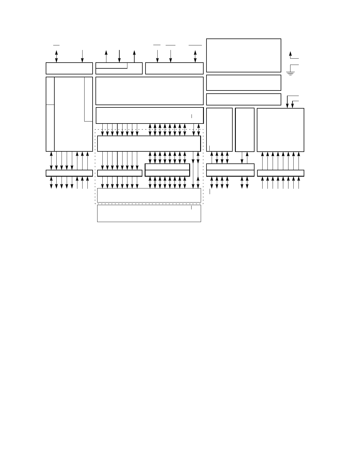
Figure 1-1 is a block diagram of the MC68HC11A8 MCU. This diagram shows the ma-
jor subsystems and how they relate to the pins of the MCU. In the lower right-hand cor-
ner of this diagram, the parallel I/O subsystem is shown inside a dashed box. The
functions of this subsystem are lost when the MCU is operated in expanded modes,
but the MC68HC24 port replacement unit can be used to regain the functions that were
lost. The functions are restored in such a way that the software programmer is unable
to tell any difference between a single-chip system or an expanded system containing
the MC68HC24. By using an expanded system containing an MC68HC24 and an ex-
ternal EPROM, the user can develop software intended for a single-chip application.
1.2 Programmer’s Model
In addition to executing all M6800 and M6801 instructions, the M68HC11 instruction
set includes 91 new opcodes. The nomenclature M68xx is used in conjunction with a
specific CPU architecture and instruction set as opposed to the MC68HC11xx nomen-
clature, which is a reference to a specific member of the M68HC11 Family of MCUs.
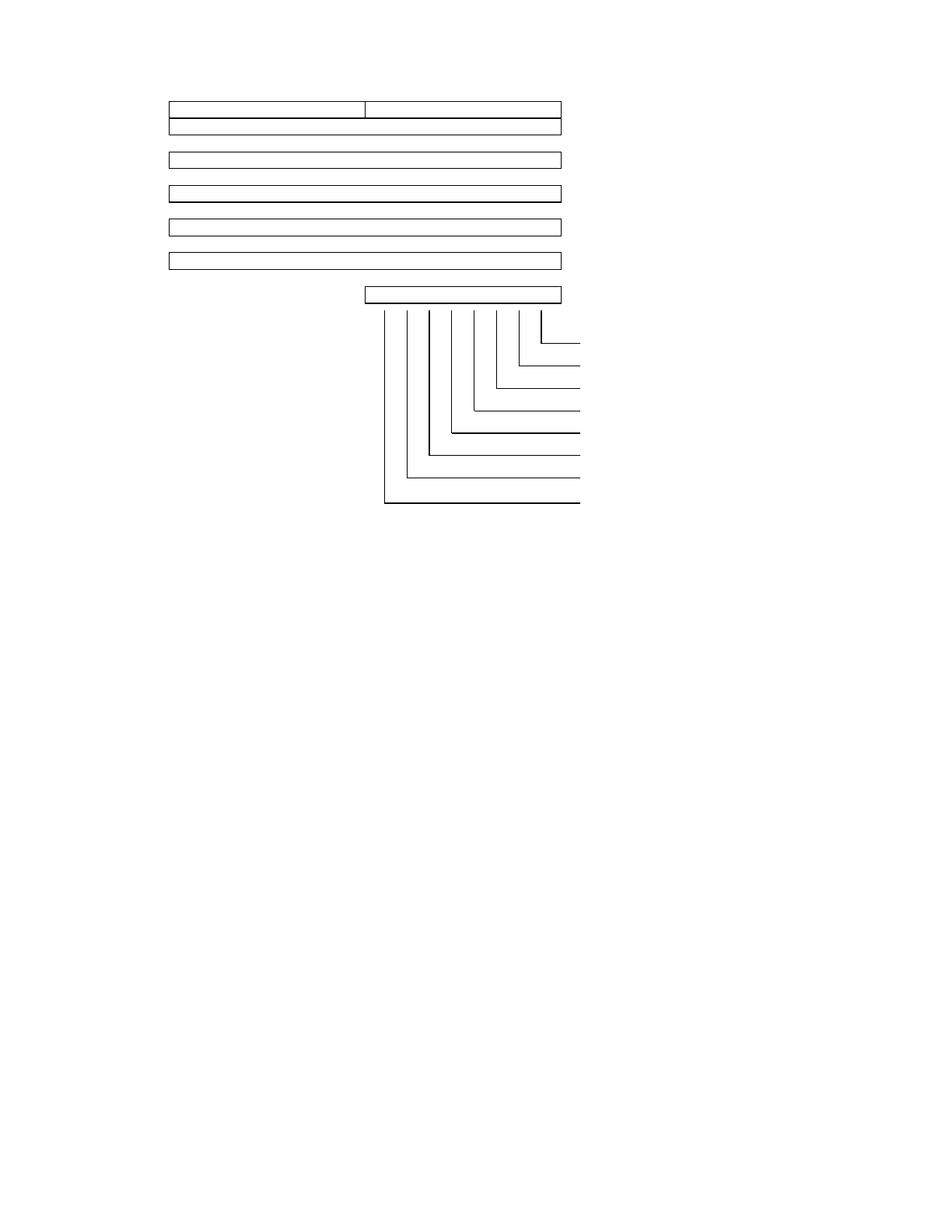
Figure 1-2 shows the seven CPU registers available to the programmer. The two 8-
bit accumulators (A and B) can be used by some instructions as a single 16-bit accu-
mulator called the D register, which allows a set of 16-bit operations even though the
CPU is technically an 8-bit processor.
The largest group of instructions added involve the Y index register. Twelve bit manip-
ulation instructions that can operate on any memory or register location were added.
The exchange D with X and exchange D with Y instructions can be used to quickly get
index values into the double accumulator (D) where 16-bit arithmetic can be used. Two
16-bit by 16-bit divide instructions are also included.
M68HC11 GENERAL DESCRIPTION MOTOROLA
REFERENCE MANUAL 1-3
Figure 1-1 Block Diagram
SPI A/D CONVERTERSCI
PORT D
CONTROL
EXTALXTAL E
OSCILLATOR
CLOCK LOGIC INTERRUPT LOGIC
MODA/
LIR MODB/
VSTBY
TIMER
SYSTEM
CPU
COPPULSE ACCUMULATOR
STROBE AND HANDSHAKE
PORT B
PB7
PB6
PB5
PB4
PB3
PB2
PB1
PB0
PORT C
PC7
PC6
PC5
PC4
PC3
PC2
PC1
PC0
STRB
STRA
PD5/SS
PD4/SCK
PD3/MOSI
PD2/MISO
PD1/TxD
PD0/RxD
PORT E
PE7/AN7
PE6/AN6
PE5/AN5
PE4/AN4
PE3/AN3
PE2/AN2
PE1/AN1
PE0/AN0
CONTROL
PORT A
PA7/PAI/OC1
PA6/OC2/OC1
PA5/OC3/OC1
PA4/OC4/OC1
PA3/OC5/OC1
PA2/IC1
PA1/IC2
PA0/IC3
BUS EXPANSION
PARALLEL I/O
ADDRESS ADDRESS/DATA
R/W
AS
SS
SCK
PERIODIC INTERRUPT
MODE
CONTROL
XIRQ
IRQ/ RESET
MOSI
MISO
256 BYTES RAM
512 BYTES EEPROM
8 KBYTES ROM
VRL
VRH
VSS
VDD
TxD
RxD
A15
A14
A13
A12
A11
A10
A9
A8
A7/D7
A6/D6
A5/D5
A4/D4
A3/D3
A2/D2
A1/D1
A0/D0
R/W
AS
SINGLE CHIP MODE
EXPANDED MODE
CIRCUITRY ENCLOSED BY DOTTED LINE IS EQUIVALENT TO MC68HC24.
MOTOROLA GENERAL DESCRIPTION M68HC11
1-4 REFERENCE MANUAL
Figure 1-2 M68HC11 Programmer’s Model
1.3 Product Derivatives
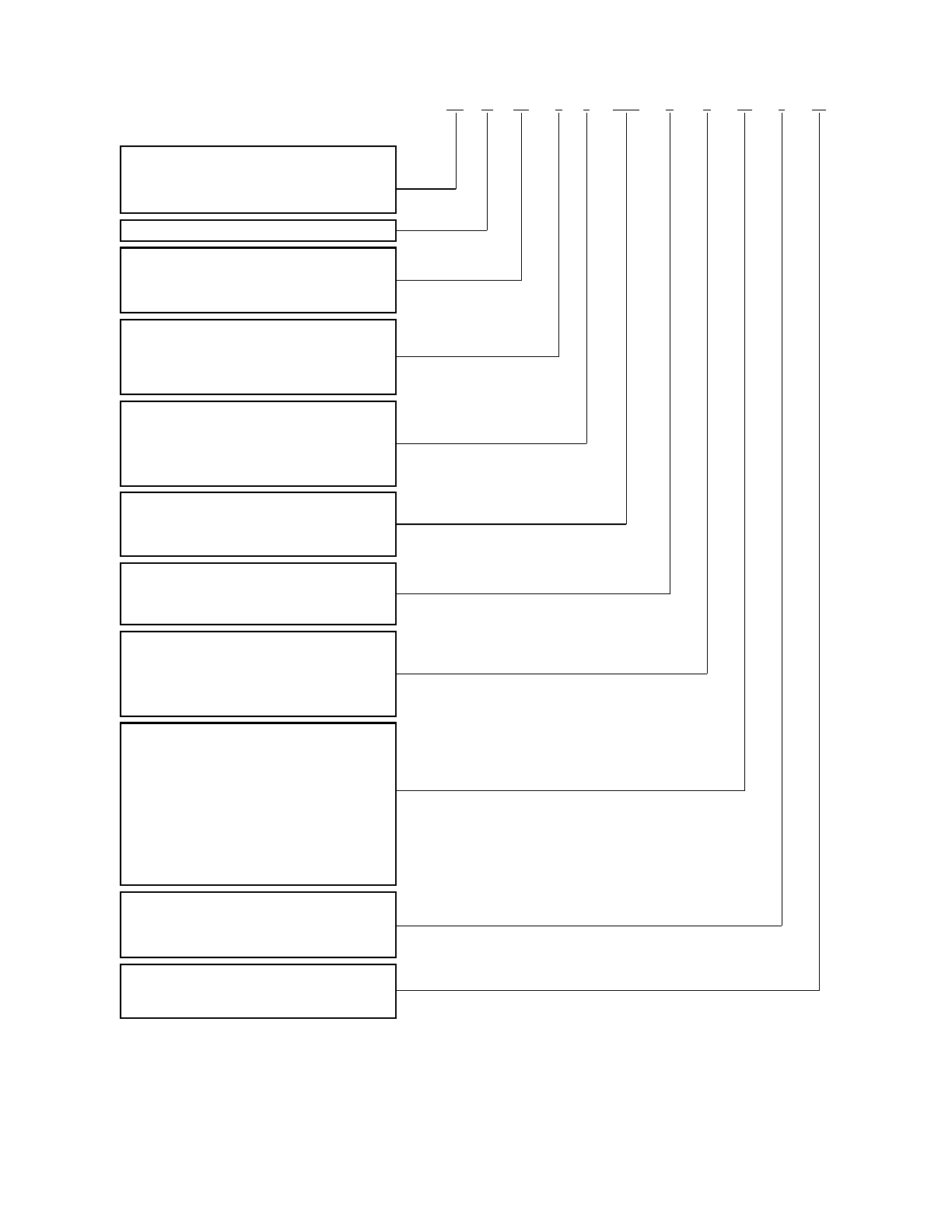
The M68HC11 Family of MCUs is composed of several members (see Table 1-1), and
new members are being developed. Figure 1-3 explains how the product part num-
bers are constructed.
8-BIT ACCUMULATORS A & B
7070
15 0
AB
D
IX
IY
SP
PC
70
CVZNIHXS
OR 16-BIT DOUBLE ACCUMULATOR
D
INDEX REGISTER X
INDEX REGISTER Y
STACK POINTER
PROGRAM COUNTER
CARRY/BORROW FROM MSB
OVERFLOW
ZERO
NEGATIVE
I-INTERRUPT MASK
HALF CARRY (FROM BIT 3)
X-INTERRUPT MASK
STOP DISABLE
CONDITION CODES
M68HC11 GENERAL DESCRIPTION MOTOROLA
REFERENCE MANUAL 1-5
Figure 1-3 Part Numbering
HC11 PART NUMBERING
MC 68 HC P 11XX B C FN 3 R2
MC — FULLY SPECIFIED AND QUALIFIED
NUMERIC DESIGNATOR (OPTIONAL)
XC — PILOT PRODUCTION DEVICE
PC — ENGINEERING SAMPLE
COP OPTION (ONLY ON A-SERIES DEVICES)
NONE —
P —
COP DISABLED
COP ENABLED
OPERATING VOLTAGE RANGE
HC — HCMOS (VDD = 5.0 VDC ±10%)
HCMOS (VDD = 3.0 VDC TO 5.5 VDC)
L —
BASE PART NUMBER
11A8, 11D3, 11E9, 11K4, ETC.
MONITOR MASK
NONE —
B — BLANK
BUFFALO
TEMPERATURE RANGE
NONE —
C —
0°C TO 70°C
– 40°C TO 85°C
– 40°C TO 105°C
V —
– 40°C TO 125°C
M —
PACKAGE TYPE
FN —
FS —
44/52/68/84-PIN PLCC
44/52/68/84-PIN CLCC
64/80-PIN QFP
FU —
MAXIMUM SPECIFIED CLOCK SPEED
2 — 2.0 MHz
3.0 MHz
3 — 4.0 MHz
4 —
MEMORY TYPE
BLANK —
7 —
MASKED ROM OR NO ROM
EPROM/OTPROM
8 — EEPROM
44-PIN QFP
FB —
112-PIN TQFP
PV —
80/100-PIN TQFP
PU —
52-PIN TQFP
PB —
TAPE AND REEL OPTION
NONE —
R2 — STANDARD PACKAGING
TAPE AND REEL PACKAGING
7
QUALIFICATION LEVEL
40/48-PIN DIP
P —
48-PIN SDIP
S —

MOTOROLA GENERAL DESCRIPTION M68HC11
1-6 REFERENCE MANUAL
1.The EEPROM is relocatable to the top of any 4 Kbyte memory page. Relocation is done with the upper four bits
of the CONFIG register.
2. CONFIG register values in this table reflect the value programmed prior to shipment from Motorola.
3. At the time of this printing a change was being considered that would make this value $0F.
Table 1-1 M68HC11 Family Members
Part Number EPROM ROM EE-
PROM RAM CONFIG2Comments
MC68HC11A8 — — 512 256 $0F Family Built Around This Device
MC68HC11A1 — — 512 256 $0D ’A8 with ROM Disabled
MC68HC11A0 — — — 256 $0C ’A8 with ROM and EEPROM Disabled
MC68HC811A
8— — 8K + 512 256 $0F EEPROM Emulator for ’A8
MC68HC11E9 — 12K 512 512 $0F Four Input Capture/Bigger RAM 12K ROM
MC68HC11E1 — — 512 512 $0D ’E9 with ROM Disabled
MC68HC11E0 — — — 512 $0C ’E9 with ROM and EEPROM Disabled
MC68HC811E
2——
2K1256 $FF3No ROM Part for Expanded Systems
MC68HC711E
912K — 512 512 $0F One-Time Programmable Version of ’E9
MC68HC11D3 — 4K — 192 N/A Low-Cost 40-Pin Version
MC68HC711D
94K — — 192 N/A One-Time Programmable Version of ’D3
MC68HC11F1 — — 51211K $FF3High-Performance Non-Multiplexed 6B-Pin
MC68HC11K4 — 24K 640 768 $FF > 1 Mbyte memory space, PWM, CS, 84-Pin
MC68HC711K
424K — 640 768 $FF One-Time Programmable Version of ’K4
MC68HC11L6 — 16K 512 512 $0F Like ’E9 with more ROM and more I/O, 64/
68
MC68HC711L6 16K — 512 512 $0F One-Time Programmable Version of ’L4

M68HC11 PINS AND CONNECTIONS MOTOROLA
REFERENCE MANUAL 2-1
SECTION 2
PINS AND CONNECTIONS
This section discusses the functions of each pin on the MC68HC11A8. Most pins on
this microcontroller unit (MCU) serve two or more functions. Information about the
practical use of each pin is presented in these pin descriptions. This section also in-
cludes information concerning pins that are exposed to illegal levels or conditions. The
most common source of illegal levels or conditions is transient noise; however, a de-
signer may wish to take precautions against potential misapplication of a product or
failures of other system components such as power supplies. Consideration of these
factors can influence end-product reliability.
The basic connections for single-chip-mode and expanded-mode applications are pre-
sented in 2.5 Typical Single-Chip-Mode System Connections and 2.6 Typical Ex-
panded-Mode-System Connections. These basic systems can be used as the
starting point for any user application and can minimize the time required to achieve a
working prototype system. The explanation of these basic systems includes informa-
tion concerning additions, such as additional memory on the expanded system.
System noise generation and susceptibility primarily depend on each system and its
environment. The MC68HC11A8 is designed for higher bus speeds than earlier
MCUs; since it is high-density complementary metal-oxide semiconductor (HCMOS),
signals drive from rail to rail, unlike earlier N-channel metal-oxide semiconductor
(NMOS) processors. Since these factors can significantly affect noise issues, the sys-
tem designer should consider these changes.
2.1 Packages And Pin Names
The following figures show pin assignments for several members of the M68HC11
MCU Family. The pin assignments for the MC68HC24 port replacement unit (PRU)
are also presented for reference although the PRU is not discussed in detail in this
manual.
Detailed mechanical data for packages may be found in the data sheets or technical
summaries. Ordering information, which relates part number suffixes to package types
and operating temperature range, are also found in the data sheets or technical sum-
maries.
2.1.1 MC68HC11A8
The MC68HC11A8 is available in either a 52-pin plastic leaded chip carrier (PLCC)
package or a 48-pin dual-in-line package (DIP). The silicon die is identical for both
packages, but four of the analog-to-digital (A/D) converter inputs are not bonded out
to pins in the 48-pin DIP. The MC68HC11A1 and MC68HC11A0 devices also use the
same die as the MC68HC11A8, except that the contents of the nonvolatile CONFIG
register determine whether or not internal read-only memory (ROM) and/or electrically

MOTOROLA PINS AND CONNECTIONS M68HC11
2-2 REFERENCE MANUAL
erasable programmable ROM (EEPROM) are disabled. These downgraded device
versions have identical pin assignments as the MC68HC11A8.
Figure 2-1 shows the pin assignments for the MC68HC11A8 in the 52-pin PLCC pack-
age and the 48-pin DIP package.
Figure 2-1 MC68HC11A8 Pin Assignments
2.1.2 MC68HC11D3/711D3
The MC68HC11D3 is available in either a 44-pin PLCC package or a 40-pin DIP pack-
age. The silicon die is identical for both packages, but the PLCC version has two ad-
ditional output compare pins bonded out and an extra VSS pin named EVSS. The
MC68HC711D3 is functionally equivalent to the MC68HC11D3 but has 4 Kbytes of
EPROM instead of mask programmed ROM. The MC68HC711D3 is available as a
one-time-programmable (OTP) MCU in an opaque plastic package or in a ceramic
windowed package for development applications.
Figure 2-2 shows the pin assignments for the MC68HC11D3/711D3 in the 44-pin
PLCC package and the 40-pin DIP package.
XTAL
PC0/A0/D0
PC1/A1/D1
PC2/A2/D2
PC3/A3/D3
PC4/A4/D4
PC5/A5/D5
PC6/A6/D6
PC7/A7/D7
RESET
XIRQ
IRQ
PD0/RxD
PE4/AN4
PE0/AN0
PB0/A8
PB1/A9
PB2/A10
PB3/A11
PB4/A12
PB5/A13
PB6/A14
PB7/A15
PA0/IC3
EXTAL
STRB/R/W
E
STRA/AS
MODA/LIR
MODB/VSTBY
VSS
VRH
VRL
PE7/AN7
PE3/AN3
PD1/TxD
PD2/MISO
PD3/MOSI
PD4/SCK
PD5/SS
VDD
PA7/PAI/OC1
PA6/OC2/OC1
PA5/OC3/OC1
PA4/OC4/OC1
PA3/OC5/OC1
8
9
10
11
12
13
14
15
16
17
44
43
42
41
40
39
38
37
36
35
34
21
22
23
24
25
26
27
28
29
30
31
7
6
5
4
3
1
2
52
51
50
49
18
19
PA2/IC1 32
PA1/IC2 33
PE6/AN648
PE2/AN2
47
PE1/AN1
45
PE5/AN5
46
20
MC68HC11A8
PB7/A15
PB6/A14
PB5/A13
PB4/A12
PB3/A11
PB2/A10
PB1/A9
PB0/A8
PE0/AN0
PE1/AN1
9
10
11
12
13
14
15
16
17
18
PE2/AN2 19
PE3/AN3 20
21
VRH 22
VSS 23
MODB/V
STBY 24
PA0/IC3 8
PA1/IC2 7
PA2/IC1 6
PA3/OC5/OC1 5
PA4/OC4/OC1 4
PA5/OC3/OC1 3
PA6/OC2/OC1 2
PA7/PAI/OC1 1
PC7/A7/D7
PC6/A6/D6
PC5/A5/D5
PC4/A4/D4
PC3/A3/D3
PC2/A2/D2
PC1/A1/D1
PC0/A0/D0
XTAL
EXTAL
STRB/R/W
38
37
36
35
34
33
32
31
30
29
28
RESET
39
XIRQ
40
E
27
STRA/AS
26
MODA/LIR
25
IRQ
41
PD0/RxD
42
PD1/TxD
43
PD2/MISO
44
PD3/MOSI
45
PD4/SCK
46
PD5/SS
47
VDD
48
VRL
MC68HC11A8

M68HC11 PINS AND CONNECTIONS MOTOROLA
REFERENCE MANUAL 2-3
Figure 2-2 MC68HC11D3/711D3 Pin Assignments
2.1.3 MC68HC11E9/711E9
The MC68HC11E9 is available in a 52-pin PLCC package only. The MC68HC11E1
and MC68HC11E0 devices also use the same die as the MC68HC11E9, except that
the contents of the nonvolatile CONFIG register determine whether or not internal
ROM and/or EEPROM are disabled. These downgraded device versions have identi-
cal pin assignments as the MC68HC11E9.
The MC68HC11E9 is an upgrade of the MC68HC11A8. The MC68HC11E9 has 12
Kbytes of mask ROM, 512 bytes of EEPROM, and 512 bytes of RAM. The timer sys-
tem allows one output-compare channel to be reconfigured as a fourth input-capture
channel.
The MC68HC711E9 is functionally equivalent to the MC68HC11E9 but has 12 Kbytes
of EPROM instead of mask programmed ROM. The MC68HC711E9 is available as a
one-time programmable (OTP) MCU in an opaque plastic package or in a ceramic win-
dowed package for development applications.
Figure 2-3 shows the pin assignments for the MC68HC11E9 in the 52-pin PLCC pack-
ages. These pin assignments are the same as the MC68HC11A8, except for the pin
name for the PA3/OC5/IC4/OC1 pin.
PC4/ADDR4
PC5/ADDR5
PC6/ADDR6
PC7/ADDR7
XIRQ/VPP
PD7/R/W
PD6/AS
RESET
IRQ
PD0/RxD
PD1/TxD
PB2/ADDR10
PB3/ADDR11
PB4/ADDR12
PB5/ADDR13
PB6/ADDR14
PB7/ADDR15
NC
PA0/IC3
PA1/IC2
PC3/ADDR3
PC2/ADDR2
PC1/ADDR1
PC0/ADDR0
VSS
EVSS
XTAL
EXTAL
E
MODA/LIR
MODB/VSTBY
PD2/MISO
PD3/MOSI
PD4/SCK
PD5/SS
VDD
PA7/PAI/OC1
PA6/OC2/OC1
PA5/OC3/OC1
PA4/OC4/OC1
PA3/IC4/OC5/OC1
PA2/IC1
7
8
9
10
11
12
13
14
15
16
37
36
35
34
33
32
31
30
29
18
19
20
21
22
23
24
25
26
27
28
6
5
4
3
2
1
44
43
42
41
40
17
PB1/ADDR9
38
PB0/ADDR8
39
MC68HC(7)11D3
PC7/ADDR7
XIRQ/VPP
PD7/R/W
PD6/AS
RESET
IRQ
PD0/RxD
PD1/TxD
PD2/MISO
PD3/MOSI
9
10
11
12
13
14
15
16
17
18
PD4/SCK 19
PD5/SS 20
PC6/ADDR6 8
PC5/ADDR5 7
PC4/ADDR4 6
PC3/ADDR3 5
PC2/ADDR2 4
PC1/ADDR1 3
PC0/ADDR0 2
VSS 1
PB5/ADDR13
PB6/ADDR14
PB7/ADDR15
PA0/IC3
PA1/IC2
PA2/IC1
PA3/IC4/OC5/OC1
PA5/OC3/OC1
PA7/PAI/OC1
VDD
30
29
28
27
26
25
24
23
22
21
PB4/ADDR12
31
PB3/ADDR11
32
PB2/ADDR10
33
PB1/ADDR9
34
PB0/ADDR8
35
MODB/VSTBY
36
MODA/LIR
37
E
38
EXTAL
39
XTAL
40
MC68HC(7)11D3

MOTOROLA PINS AND CONNECTIONS M68HC11
2-4 REFERENCE MANUAL
Figure 2-3 MC68HC11E9/711E9 Pin Assignments (52-Pin PLCC)
2.1.4 MC68HC811E2
The MC68HC811E2 is very similar to the MC68HC11E9 version, except in the on-chip
memory. The MC68HC811E2 includes 2 Kbytes of EEPROM, which can be remapped
to the upper half of any 4 Kbyte page in the 64 Kbyte map. There is no masked ROM
memory in the MC68HC811E2. The MC68HC811E2 is available in either a 52-pin
PLCC package or a 48-pin DIP. The silicon die used is the same for both packages,
but four of the A/D converter inputs are not bonded out to pins in the 48-pin package.
The MC68HC811E2 version replaces an earlier version called the MC68HC811A2.
The only significant difference between the MC68HC811E2 and MC68HC811A2 is
that the MC68HC811E2 has a slightly more flexible timer system, which allows one
output-compare channel to be reconfigured as a fourth input-capture channel.
The 52-pin PLCC package version of the MC68HC811E2 has identical pin assign-
ments to the MC68HC11E9 pin assignments shown in Figure 2-3.Figure 2-4 illus-
trates the pin assignments for the MC68HC811E2 in the 48-pin DIP.
XTAL
PC0/A0/D0
PC1/A1/D1
PC2/A2/D2
PC3/A3/D3
PC4/A4/D4
PC5/A5/D5
PC6/A6/D6
PC7/A7/D7
RESET
XIRQ
IRQ
PD0/RxD
PE4/AN4
PE0/AN0
PB0/A8
PB1/A9
PB2/A10
PB3/A11
PB4/A12
PB5/A13
PB6/A14
PB7/A15
PA0/IC3
EXTAL
STRB/R/W
E
STRA/AS
MODA/LIR
MODB/VSTBY
VSS
VRH
VRL
PE7/AN7
PE3/AN3
PD1/TxD
PD2/MISO
PD3/MOSI
PD4/SCK
PD5/SS
VDD
PA7/PAI/OC1
PA6/OC2/OC1
PA5/OC3/OC1
PA4/OC4/OC1
PA3/OC5/OC1
8
9
10
11
12
13
14
15
16
17
44
43
42
41
40
39
38
37
36
35
34
21
22
23
24
25
26
27
28
29
30
31
7
6
5
4
3
1
2
52
51
50
49
18
19
PA2/IC1 32
PA1/IC2 33
PE6/AN648
PE2/AN2
47
PE1/AN1
45
PE5/AN5
46
20
MC68HC11E9

M68HC11 PINS AND CONNECTIONS MOTOROLA
REFERENCE MANUAL 2-5
Figure 2-4 MC68HC811E2 Pin Assignments (48-Pin DIP)
2.1.5 MC68HC11F1
The MC68HC11F1 is available in a 68-pin PLCC package only. The MC68HC11F1 is
the first non-multiplexed address/data bus version of the M68HC11 family. In addition
to the non-multiplexed bus, this MCU includes 1 Kbyte of on-chip RAM and intelligent
chip selects for simple connection to external program memory without the need for
any external logic chips. Other on-chip peripherals are similar to the MC68HC11E9.
Figure 2-5 shows the pin assignments for the MC68HC11F1 in the 68-pin PLCC pack-
age.
PB7/A15
PB6/A14
PB5/A13
PB4/A12
PB3/A11
PB2/A10
PB1/A9
PB0/A8
PE0/AN0
PE1/AN1
9
10
11
12
13
14
15
16
17
18
PE2/AN2 19
PE3/AN3 20
21
VRH 22
VSS 23
MODB/V
STBY 24
PA0/IC3 8
PA1/IC2 7
PA2/IC1 6
PA3/OC5/OC1 5
PA4/OC4/OC1 4
PA5/OC3/OC1 3
PA6/OC2/OC1 2
PA7/PAI/OC1 1
PC7/A7/D7
PC6/A6/D6
PC5/A5/D5
PC4/A4/D4
PC3/A3/D3
PC2/A2/D2
PC1/A1/D1
PC0/A0/D0
XTAL
EXTAL
STRB/R/W
38
37
36
35
34
33
32
31
30
29
28
RESET
39
XIRQ
40
E
27
STRA/AS
26
MODA/LIR
25
IRQ
41
PD0/RxD
42
PD1/TxD
43
PD2/MISO
44
PD3/MOSI
45
PD4/SCK
46
PD5/SS
47
VDD
48
VRL
MC68HC811E2

MOTOROLA PINS AND CONNECTIONS M68HC11
2-6 REFERENCE MANUAL
Figure 2-5 MC68HC11F1 Pin Assignments (68-Pin PLCC)
2.1.6 MC68HC24 Port Replacement Unit
The MC68HC24 is available in either a 44-pin PLCC package or a 40-pin DIP. Figure
2-6 shows the pin assignments for the MC68HC24 in the 44-pin PLCC package and
the 40-pin DIP package.
DATA1/PC1
DATA2/PC2
DATA3/PC3
DATA4/PC4
DATA5/PC5
DATA6/PC6
DATA7/PC7
RESET
XIRQ
IRQ
CSPROG/PG7
CSGEN/PG6
CSIO1/PG5
PF0/ADDR0
PF1/ADDR1
PF2/ADDR2
PF3/ADDR3
PF4/ADDR4
PF5/ADDR5
PF6/ADDR6
PF7/ADDR7
PB0/ADDR8
PB1/ADDR9
PB2/ADDR10
DATA0/PC0
4XOUT
XTAL
EXTAL
R/W
E
VSS
VRH
VRL
MODA/LIR
PG0
RxD/PD0
TxD/PD1
MISO/PD2
MOSI/PD3
SCK/PD4
SS/PD5
VDD
PAI/OC1/PA7
OC2/OC1/PA6
OC3/OC1/PA5
10
11
12
13
14
15
16
17
18
19
58
57
56
55
54
53
52
51
50
49
48
27
28
29
30
31
32
33
34
35
36
37
9
8
7
6
5
1
4
2
68
67
20
21
OC4/OC1/PA4 38
OC5/OC1/PA3 39
PE7/AN766
65
PE0/AN0
59
PE4/AN4
60
22
PE3/AN3
PE6/AN6
PE2/AN2
64
63
PE5/AN562
PE1/AN2
61
IC1/PA2
IC2/PA1
40
41
IC3/PA0 42
ADDR15/PB7 43
3
CSIO2/PG4
PG3
PG2
PG1
PB3/ADDR11
PB4/ADDR12
PB5/ADDR13
PB6/ADDR14
23 47
46
45
44
24
25
26
MODB/VSTBY
MC68HC11F1

M68HC11 PINS AND CONNECTIONS MOTOROLA
REFERENCE MANUAL 2-7
Figure 2-6 MC68HC24 Pin Assignments
2.2 Pin Descriptions
This section provides a pin-by-pin description of the MCU. In general, a designer
should consider all possible functions of each pin when designing the MCU into an ap-
plication system. SECTION 7 PARALLEL INPUT/OUTPUT contains transistor-level
schematics of the logic associated with each of the I/O pins. SECTION 3 CONFIGU-
RATION AND MODES OF OPERATION discusses the pins that operate as a multi-
plexed address/data bus in expanded modes of operation as well as the functions of
other pins related to mode selection and bus control. The reset and interrupt pins are
presented again in SECTION 5 RESETS AND INTERRUPTS. Sections 8 through 12
discuss pins related to the on-chip peripherals presented in those sections.
Figure 2-1 is a pin-function-oriented block diagram of the MC68HC11A8, which is a
good reference for development and verification of application designs.
2.2.1 Power-Supply Pins (VDD and VSS)
Power is supplied to the MCU by using these pins. VDD is the positive power input, and
VSS is ground. The MC68HC11A8 MCU uses a single power supply, but in some ap-
plications, there may also be optional power supplies for A/D reference and/or for bat-
tery backup of on-chip random-access memory (RAM). These additional power
sources are optional, and the MCU, including RAM and A/D, can operate from a single
5-V (nominal) power supply.
STRA
PC0
PC1
PC2
PC3
NC
PC4
PC5
PC6
PC7
VDD
AD1
AD2
AD3
NC
AD4
AD5
AD6
AD7
VSS
A12
A13
A14
A15
I/O TEST
NC
CS
MODE
AS
E
R/W
STRB
PB7
PB6
PB5
PB4
NC
PB3
PB2
PB1
PB0
IRQ
7
8
9
10
11
12
13
14
15
16
37
36
35
34
33
32
31
30
29
18
19
20
21
22
23
24
25
26
27
28
6
5
4
3
2
1
44
43
42
41
40
17
AD0
38
RESET
39
MC68HC24 PC2
PC3
PC4
PC5
PC6
PC7
VDD
STRB
PB7
PB6
9
10
11
12
13
14
15
16
17
18
PB5 19
PB4 20
PC1 8
PC0 7
STRA 6
A12 5
A13 4
A14 3
A15 2
I/O TEST 1
AD4
AD5
AD6
AD7
VSS
IRQ
PB0
PB1
PB2
PB3
30
29
28
27
26
25
24
23
22
21
AD3
31
AD2
32
AD1
33
AD0
34
RESET
35
R/W
36
E
37
AS
38
MODE
39
CS
40
MC68HC24

MOTOROLA PINS AND CONNECTIONS M68HC11
2-8 REFERENCE MANUAL
Although the MC68HC11A8 is a CMOS device, very fast signal transitions are present
on many of the pins. Even when the MCU is operating at slow clock rates, short rise
and fall times are present. Depending upon the loading on these fast signals, signifi-
cant short-duration current demands can be placed on the MCU power supply. Special
care must be taken to provide good power-supply bypassing at the MCU.
The faster edge times in the MC68HC11A8 generally place greater demands on by-
passing than earlier NMOS MCU designs. A typical expanded-mode system should in-
clude a 1-µF capacitor and a separate 0.01-µF capacitor. Both these capacitors
should be as close (physically and electrically) as possible to the MC68HC11A8 and
should have good high-frequency characteristics (i.e., not old-technology dipped ce-
ramic disc). The 1-µF capacitor primarily supplies charge for bus switching through a
very low-impedance path (minimum-length runners). Without this bypass, there could
be very large voltage drops in the circuit board runners to the MCU due to the very high
(although very short duration) current spike caused by several MCU pins simulta-
neously switching from one level to the other. The separate 0.01-µF capacitor is in-
cluded because the larger 1-µF capacitor is typically not as good at snubbing very
high-frequency (low energy) noise. These are only general recommendations. Some
lightly loaded single-chip systems may work quite well with a single 0.1-µF bypass ca-
pacitor; whereas, more heavily loaded expanded-mode systems may require more
elaborate bypassing measures.
It is easier and less expensive to approach power-supply layout and bypassing as a
preventive measure from the beginning of a design than to locate and correct a noise
problem in a marginal design. Problems related to inadequate power-supply layout
and bypassing are very difficult to locate and correct, but, if reasonable care is taken
from the start of a design, noise should not arise as a problem.
2.2.2 Mode Select Pins (MODB/VSTBY and MODA/LIR)
The mode B/standby RAM supply (MODB/VSTBY) pin functions as both a mode select
input pin and a standby power-supply pin. The mode A/load instruction register (MO-
DA/LIR) pin is used to select the MCU operating mode while the MCU is in reset, and
it operates as a diagnostic output signal while the MCU is executing instructions.
The hardware mode select mechanism starts with the logic levels on the MODA and
MODB pins while the MCU is in the reset state. The logic levels on the MODA and
MODB pins are fed into the MCU via a clocked pipeline path. The levels captured are
those that were present part of a clock cycle before the RESET pin rose, which as-
sures there will be a zero hold-time requirement on the mode select pins relative to the
rising edge at the RESET pin. The captured levels determine the logic state of the spe-
cial mode (SMOD) and mode A select (MDA) control bits in the highest priority inter-
rupt (HPRIO) register. These two control bits actually control the logic circuits involved
in hardware mode selection. Mode A selects between single-chip modes and expand-
ed modes; mode B selects between the normal variation and the special variation of
the chosen operating mode. Bootstrap mode is the special variation of single-chip
mode, and special test is the special variation of expanded mode. Table 2-1 summa-
rizes the operation of the mode pins and mode control bits.

M68HC11 PINS AND CONNECTIONS MOTOROLA
REFERENCE MANUAL 2-9
After reset is released, the mode select pins no longer influence the MCU operating
mode. The MODA pin serves the alternate function of load instruction register (LIR)
when the MCU is not in reset. The open-drain active-low LIR output pin drives low dur-
ing the first E cycle of each instruction. The MODB pin serves the alternate function of
a standby power supply (VSTBY) to maintain RAM contents when VDD is not present.
The power-saving mode, STOP, is an alternate way to save RAM contents, which
does not require a separate standby power source.
The LIR function is intended for monitoring on a logic analyzer during debug of a sys-
tem. Since this status indicator shows where each instruction begins, programs can
be followed easily. The mode A select levels and the LIR status levels were selected
to prevent interference between the shared functions of the pin. In single-chip applica-
tions, this pin is simply connected to VSS. Since the LIR output is open-drain, there is
no conflict between the direct VSS connection and the LIR signal that drives the pin low
during the first E cycle of each instruction. There is no practical reason to monitor LIR
during single-chip modes because there is no visibility to internal data and address
buses. In expanded-mode systems, the MODA/LIR pin is normally pulled up to VDD by
a 4.7 kΩresistor. During reset, the pull-up resistor instructs the MODA pin to select
expanded modes. During-program execution, the pin is driven low during the first cycle
of each instruction by the LIR signal and is pulled up between LIR signals by the ex-
ternal 4.7 kΩ pull-up.
In expanded-mode systems where it is important to minimize power-supply current,
logic could be used to drive the MODA/LIR pin rather than just using a simple pull-up
(see Figure 2-7). During reset, the MODA pin would be driven high to select expanded
mode. After reset, the LIR pin would be driven low by logic. The logic should not be
operating against a pull-up, but rather it should be a logic-gate-type output with some
series resistance to protect against the unlikely event of a conflict between an active-
low LIR signal and an active-high logic-gate output signal. Such a conflict could only
occur briefly at the falling edge of reset. Since LIR is active for about one out of every
three cycles during normal execution (average instructions take about three cycles),
IDD could be reduced by about 350 µA (5 V ÷ 4.7 kΩ x 33% duty cycle).
Table 2-1 Hardware Mode Select Summary
Inputs Mode Description Control Bits in HPRIO (Latched at Reset)
MODB MODA RBOOT SMOD MDA IRV
1 0 Normal Single Chip 0000
1 1 Normal Expanded 0010
0 0 Special Bootstrap 1101
0 1 Special Test 0111

MOTOROLA PINS AND CONNECTIONS M68HC11
2-10 REFERENCE MANUAL
Figure 2-7 Reduced IDD MODA/LIR Connections
The VSTBY function is accomplished by a transistor switch that connects either VSTBY
or VDD to the RAM and reset logic, depending upon the relative levels of VSTBY and
VDD. The switch connects VDD unless VSTBY is more than a threshold higher than VDD.
A threshold is approximately a diode drop (0.7 V) but varies from lot to lot due to pro-
cessing variations. During normal operation of the MCU, VDD is supplying power to the
RAM. In a standby situation, VSTBY should be maintained at a valid level, and RESET
should be activated (pulled low) when VDD drops below legal limits. RESET should al-
ways be held low whenever VDD is below its operating limit. If the MCU is to be oper-
ated in a special mode (MODB low before applying reset) and the MODB/VSTBY pin is
being used to back up the RAM, the MODB/VSTBY pin should not be driven low unless
VDD is at (has returned to) a legal level. Some logic may be required in systems that
use MODB/VSTBY as a standby supply and wish to use one of the special modes of
operation. In most applications, the MODB pin would be connected to VDD through a
4.7 kΩ pull-up resistor for normal modes or directly to ground for special modes.
There are two ways to maintain the contents of on-chip RAM with minimal power con-
sumption (as in a battery-based application). The preferred method uses the STOP
mode of operation, and the second method uses the MODB/VSTBY pin (see Figure 2-
8). Each of these methods has advantages. The STOP method is preferred because
it is much simpler than the separate power-supply method in terms of hardware costs
and complexity. The STOP method saves power by stopping all MCU clocks, which
reduces the VDD current to a few microamps. No external logic is needed, and the con-
tents of internal registers are maintained in addition to the contents of internal RAM.
The MODB/VSTBY pin method would be used in cases where there is a significant
amount of external circuitry operating from VDD so that the added complexity of two
supplies and added logic is justified by the power savings.
4.7K
RESET
74HC04
TO MODA/LIR
OF M68HC11
M68HC11 PINS AND CONNECTIONS MOTOROLA
REFERENCE MANUAL 2-11
Figure 2-8 RAM Standby MODB/VSTBY Connections
2.2.3 Crystal Oscillator and Clock Pins (EXTAL, XTAL, and E)
The oscillator pins can be used with an external crystal network or an externally gen-
erated CMOS-compatible clock source. The frequency applied to these pins is four
times higher than the desired bus frequency (E-clock rate). The E clock is the bus fre-
quency clock output, which is used as a basic timing reference signal. When the E
clock is low (address portion of a bus cycle), an internal process is occurring; when E
is high, data is being addressed. The E clock is free running at one-fourth the crystal
frequency as long as the oscillator is active (STOP stops all clocks).
The oscillator in the MC68HC11A8 consists of a large two-input NAND gate. One of
the inputs to this gate is driven by an internal signal that disables the oscillator when
the MCU is in the STOP mode. The other input is the EXTAL input pin of the MCU.
The output of this NAND gate is the XTAL output pin of the MCU.
The XTAL pin is normally left unterminated when using an external CMOS-compatible
clock input to the EXTAL pin. However, a 10 kΩ-100 kΩload resistor to ground may
be used to reduce generated radio frequency interference (RFI) noise emission. The
XTAL output is normally intended to drive only a crystal, but XTAL can be used as a 4
x clock output if special care is taken to avoid undesirable loading. The XTAL output
may be buffered with a high-impedance buffer such as the 74HC04, or it may be used
to drive the EXTAL input of another M68HC11 MCU. In all cases, the circuit-board lay-
out around the oscillator pins is critical. Load capacitances specified in the data sheets
and technical summary include all stray layout capacitances. Thus, the physical ca-
pacitors connected to these pins should always be less than the specified load capac-
itances by the estimated interconnection capacitances.
Figure 2-9 and Figure 2-10 show the internal and external components that form the
crystal oscillator, called a Pierce oscillator (also known as a parallel resonant crystal
oscillator).
Figure 2-9 shows the connections for high-frequency crystals (greater than 1 MHz),
and Figure 2-10 shows connections for low-frequency operation (less than 1 MHz).
OUT
4.7K TO MODB/V STBY
MAX
690
V
VBATT
VDD
+
4.8 V
NiCd
OF M68HC11
VDD
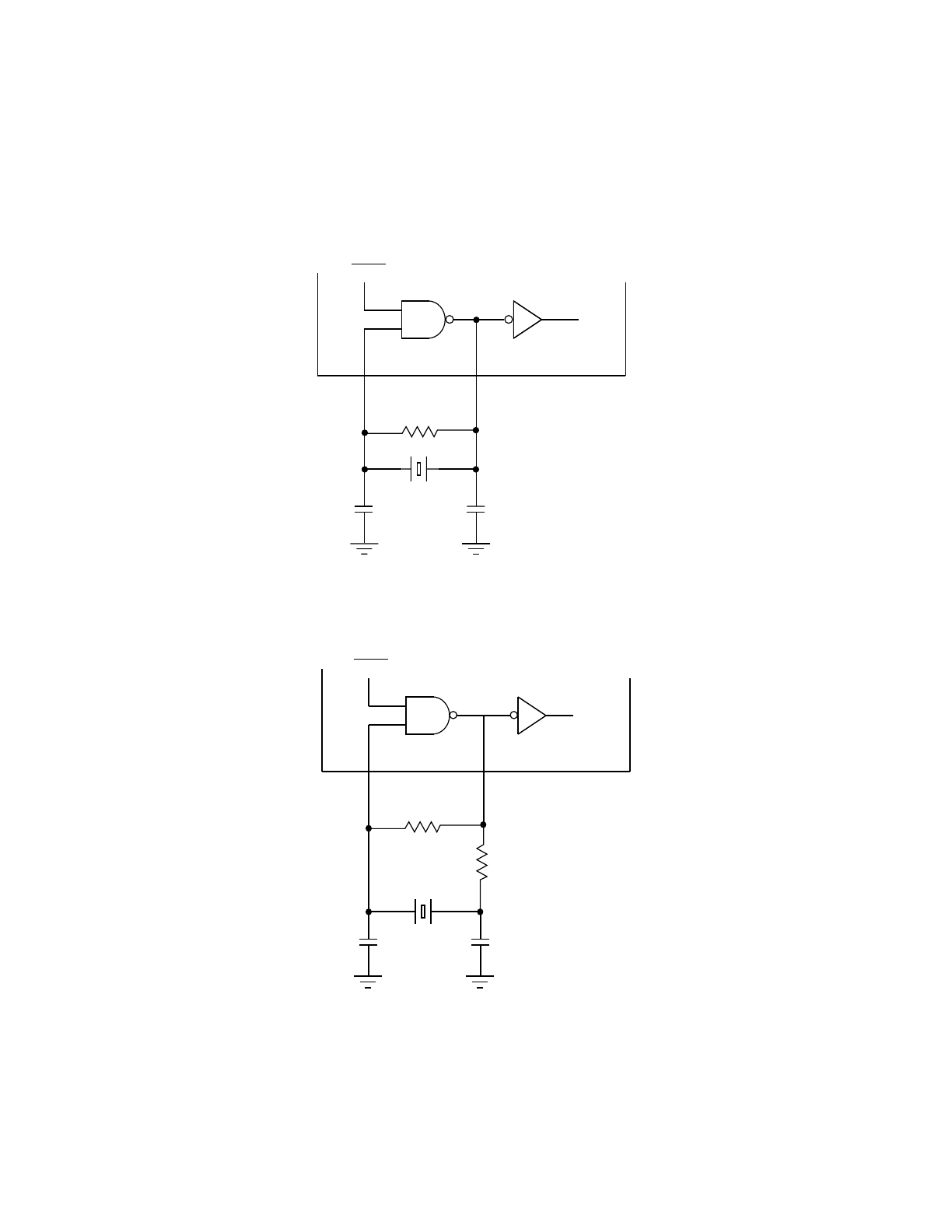
MOTOROLA PINS AND CONNECTIONS M68HC11
2-12 REFERENCE MANUAL
The resistor, Rf, provides a direct current bias to the input so the NAND operates in its
linear region. In low-frequency designs, RSand C2 provide a phase shift. RSalso limits
the power into the crystal, which is important for many small crystals because they are
designed for very low drive levels (typically 1-µW maximum). In high-frequency appli-
cations (see Figure 2-9), the output impedance of the NAND driver, combined with the
lower impedance of C1 and C2, provides the same effect as the RSin low-frequency
designs. Higher frequency AT-cut crystals are designed for much higher drive levels.
Figure 2-9 High-Frequency Crystal Connections
Figure 2-10 Low-Frequency Crystal Connections
Exact values for the external components are a function of wafer processing parame-
ters, package capacitance, printed circuit board (PCB) capacitance and inductance,
M68HC11
XTALEXTAL
Rf
C2C1
XTAL
STOP
M68HC11
XTALEXTAL
Rf
C2C1
XTAL
STOP
RS
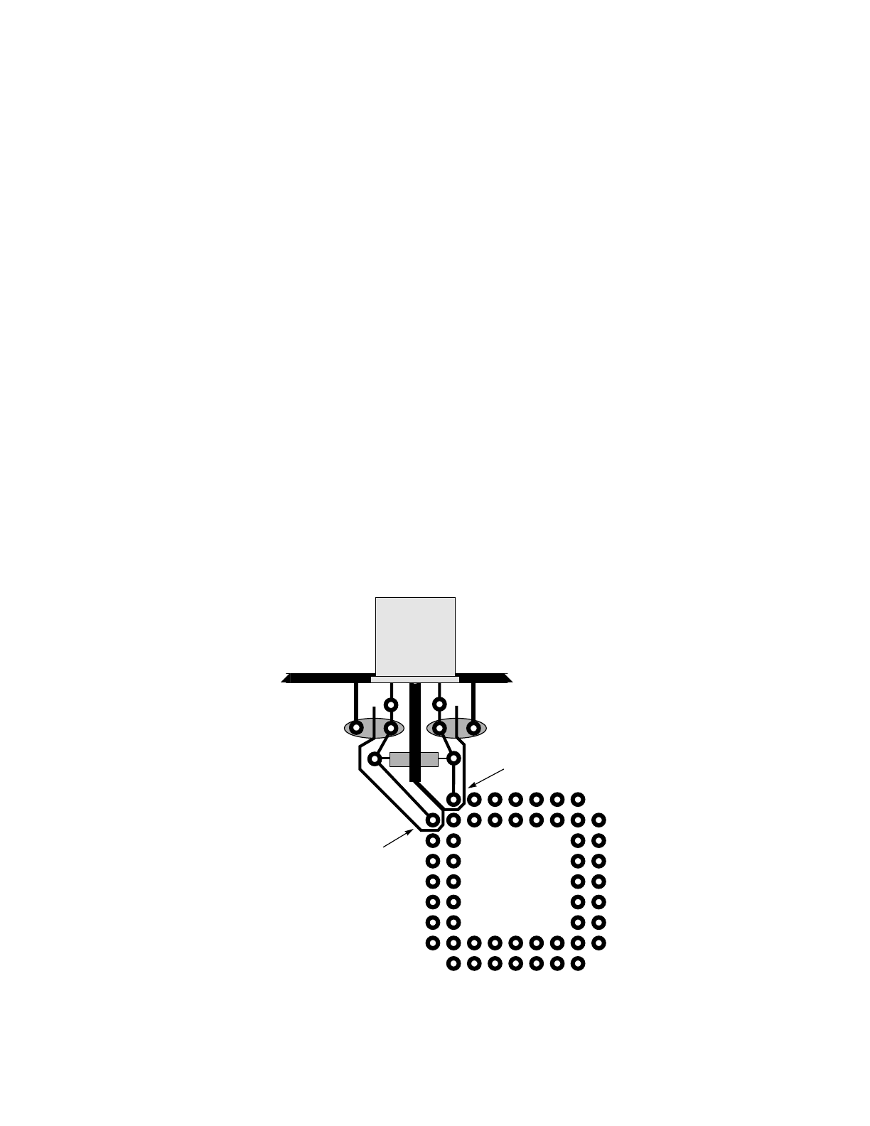
M68HC11 PINS AND CONNECTIONS MOTOROLA
REFERENCE MANUAL 2-13
socket capacitance, operating voltage, crystal technology, and frequency. Typical val-
ues are as follows:
A tune-up procedure for experimentally determining RSwill be discussed at the con-
clusion of this subsection. Since circuit and layout capacitances effectively add to the
values of C1 and C2, the physical capacitances are usually smaller than the intended
capacitances.
In most high-frequency applications, the values of C1 and C2 are equal. In low-fre-
quency designs, it is often desirable to make C1 smaller than C2, which provides a
higher voltage at the EXTAL input due to an impedance transformation. The wider volt-
age swing at this input will result in lower power-supply current.
As in all crystal oscillator designs, all leads should be kept as short as possible. It is
also good practice to route VSS paths as shown in Figure 2-11. These paths isolate
the oscillator input from the output and the oscillator from adjacent circuitry, only add-
ing capacitance in parallel with C1 and C2. Potentially noisy lines should be kept as
far as possible from the oscillator components. Ground loops should be avoided
around oscillator components (note the unterminated VSS paths ending under C1 and
C2 in Figure 2-11).
Figure 2-11 Crystal Layout Example
Rf = 1 MΩ–20 MΩHigher values are sensitive to humidity; lower values reduce gain and
could prevent startup.
Cl = 5 pF–25 pF Value is usually fixed.
C2 = 5 pF–25 pF Value may be varied to trim frequency.
CRYSTAL
C1C2
Rf
PIN 7
EXTAL
PIN 8
XTAL
M68HC11
MCU

MOTOROLA PINS AND CONNECTIONS M68HC11
2-14 REFERENCE MANUAL
Usually, the operation of the oscillator cannot be observed with an oscilloscope con-
nected to one of the oscillator pins. The oscilloscope adds from 3 to 30 pF and from 1
to 10 MΩto VSS, which will usually affect oscillator operation. When the oscilloscope
is connected to the EXTAL input, the 10 MΩto VSS (oscilloscope input) forms a resis-
tive divider with Rfand often disables the oscillator by biasing the circuit out of the lin-
ear region of the EXTAL input. This problem can sometimes be overcome by
capacitively coupling the oscilloscope with a very small capacitor (1–5 pF) between
the oscilloscope probe and the oscillator pin. It is usually better to observe the E-clock
output from the MCU since this does not alter the operation of the oscillator.
In low-frequency designs, it is often possible to observe the XTAL node with an oscil-
loscope because the high-impedance nodes of the oscillator are isolated from XTAL
by RS. Observe IDD without the oscilloscope connected and again with the oscillo-
scope connected. If the IDD is unchanged, it is usually safe to assume the oscillator
was unaffected.
Low-frequency crystal circuits tend to be very high impedance. Thus, the PCB must
be clean, dry, and free of conductive material such as solder rosin and excessive mois-
ture from high humidity. If problems occur, the value of Rfcan be reduced so the con-
taminant impedance is less significant in comparison. Of course, it is still best to
eliminate the contaminants.
Usually, startup time is inversely proportional to the frequency; thus, low-frequency os-
cillators start slower than high-frequency oscillators. There are many exceptions to this
rule because there are many variables affecting startup time. Observation of a few cir-
cuits using the MC68HC11A8 with an 8-MHz crystal reveals startup from STOP takes
approximately two milliseconds, and startup from power-up occurs within a few milli-
seconds of when VDD reaches approximately one Volt. Power-up performance varies
greatly since power-source turn-on characteristics vary greatly. Since the
MC68HC11A8 is a fully static design, the oscillator is not required to be running full
speed before the processor starts executing instructions (most applications do not re-
quire a stable oscillator within the first few milliseconds after power-up). If the oscillator
is not running at full speed, instructions will take longer to execute, but no unpredict-
able behavior will result as it would in an NMOS processor. An oscillator in the 32-kHz
range could require hundreds of milliseconds or even a few seconds to start and sta-
bilize.
NOTE
The following tune-up procedure is only meaningful for crystal fre-
quencies below 1 MHz. In higher frequency applications, because RS
is normally 0 Ω, this procedure is not needed.
The value of RScan be determined experimentally by using the final PCB and an MCU
of the exact type that will be used in the final application. The MCU need not have the
final mask program because the MCU will be held in reset throughout the experiment.
Because of the number of variables involved, use components with the exact proper-
ties of those that will be used in production. For example, do not use a ceramic-pack-
aged MCU prototype for the experiment when a plastic-packaged MCU will be used in

M68HC11 PINS AND CONNECTIONS MOTOROLA
REFERENCE MANUAL 2-15
production. An emulator version of the part will also have slightly different electrical
properties than the masked ROM version of the same part.
To determine the optimum value for RS, observe the operating current (IDD)ofthe
MCU as a function of RS. The MCU should be held in reset throughout this procedure
because operating current variations during run modes are much greater than the cur-
rent variations due to varying RS. Normally, a dip in current will occur. This dip is not
sharp as in many LC circuits but is instead very broad. As the shape of this curve sug-
gests, the exact value of RS is not critical.
Finally, verify that the maximum-operating supply voltage does not overdrive the crys-
tal. Observe the output frequency as a function of VDD at the buffered E-clock output.
Under proper operating conditions, the frequency should increase a few parts per mil-
lion as supply voltage increases. If the crystal is overdriven, an increase in supply volt-
age will cause a decrease in frequency, or the frequency will become unstable. If
frequency problems arise, supply voltage must be decreased, or the values of RS, C1,
and C2 should be increased to reduce the crystal drive.
2.2.4 Crystal Oscillator Application Information
Some crystal oscillator application information is presented in the following para-
graphs.
2.2.4.1 Crystals for Parallel Resonance
Parallel resonance refers to a Pierce oscillator that has the crystal in parallel with an
inverter. Almost all (if not all) CMOS MCUs use this type oscillator. AT-cut crystals are
available as standard devices for both series resonant circuits and Pierce oscillators.
The load capacitance has to be specified for the Pierce version. The series resonant
versions do not require this specification and are more likely to be listed as a standard
product. The type circuit affects the oscillating frequency of the crystal.
Any 4- to 8-MHz AT-cut crystal will normally meet the requirements of an M68HC11.
However, for a very accurate oscillator frequency, use the Pierce version of the crystal
with C1 and C2 values to match the specified load capacitance value for the crystal.
The load capacitance is approximately equal to the series combination of C1 and C2.
2.2.4.2 Using Crystal Oscillator Outputs
The crystal oscillator is actually an RF application. Connecting the crystal pins to other
circuitry is likely to interfere with proper operation of the oscillator. Modern CMOS in-
puts are very high impedance and relatively low capacitance; thus, one of these inputs
can be connected to the oscillator without disturbing the oscillator. The data sheet
shows examples of ways the crystal oscillator can be used to drive other circuits for
crystal frequencies between 4 and 8 MHz.
2.2.4.3 Using External Oscillator
An externally built Pierce oscillator will operate like a crystal connected to the
M68HC11. Use a single inverter and connect the crystal feedback resistor and load

MOTOROLA PINS AND CONNECTIONS M68HC11
2-16 REFERENCE MANUAL
capacitors as if the external inverter input were the EXTAL pin and the inverter output
were the XTAL pin. Use a 74HCU04 for this inverter. This device is an unbuffered HC-
MOS hex inverter. Avoid Schmitt-trigger devices because the oscillator may fail to
start. Buffer the output of the external Pierce oscillator to drive additional logic.
2.2.4.4 AT-strip vs AT-cut Crystals
The AT-strip is a new-technology low-power crystal. Connecting one of these crystals
to the M68HC11 may cause problems due to the NAND gate in the MCU overdriving
the crystal. Use an AT-cut crystal with the M68HC11 to avoid this problem.
2.2.5 Reset Pin (RESET)
This active-low, bidirectional control signal is used as an input to initialize the
MC68HC11A8 to a known startup state and as an open-drain output to indicate that
an internal failure has been detected in either the clock monitor or computer operating
properly (COP) watchdog circuit. This RESET signal is significantly different from the
RESET signal used on earlier MCUs. More detailed information about this pin can be
found in SECTION 5 RESETS AND INTERRUPTS.
The reset circuitry is specifically designed to work with lower levels of VDD than other
MCU circuitry. Thus, RESET can be used to prevent undesirable performance as VDD
power is applied or decays, which is important for applications in which the contents
of on-chip RAM must be maintained in the absence of VDD. In this situation, the RAM
and reset input logic in the MCU would be powered from a standby power source con-
nected to the MODB/VSTBY pin whenever VDD is too low to support proper MCU oper-
ation. Secondly, RESET must be controlled when VDD is below legal operating limits
to prevent unintentional corruption of EEPROM data. Even if an application is not us-
ing the 512-byte EEPROM, the CONFIG register is still an EEPROM byte and must be
protected from corruption.
Virtually all MC68HC11A8 systems should include automatic control of RESET to
drive it low whenever VDD is below legal limits. A simple, inexpensive, low voltage in-
hibit (LVI) device such as the MC34064 or MC34164 can be used. The MC34064 is
available in TO-92 or SOT-8 plastic packages and provides an open-drain output to
directly drive the RESET pin of the MC68HC11A8. This device is connected to VDD,
VSS, and the RESET pin of the MCU. A pull-up resistor from RESET to VDD is the only
other component required for the reset circuit in most applications. Figure 2-12 shows
a typical reset circuit.
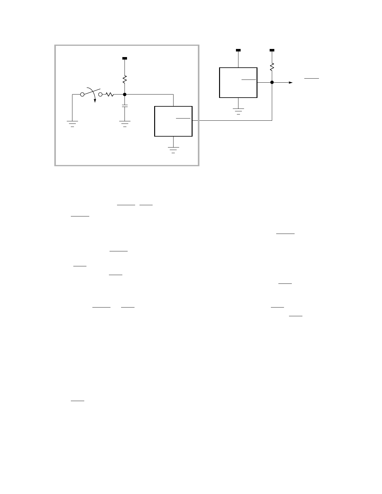
M68HC11 PINS AND CONNECTIONS MOTOROLA
REFERENCE MANUAL 2-17
Figure 2-12 Reset Circuit Example
2.2.6 Interrupt Pins (XIRQ, IRQ)
The XIRQ pin provides a means for requesting non-maskable interrupts after reset ini-
tialization. During reset, the X bit in the condition code register (CCR) is set, and any
interrupts are masked until MCU software enables them. Since the XIRQ input is level
sensitive, it can be connected to a multiple-source wired-OR network with an external
pull-up resistor. XIRQ is often used as a power loss detect interrupt.
The IRQ input provides a means for requesting asynchronous interrupts to the
MC68HC11A8. IRQ is program selectable (OPTION register), having a choice of ei-
ther level-sensitive or falling-edge-sensitive triggering. After reset, IRQ is configured
for level-sensitive operation by default.
Whenever XIRQ or IRQ are used with multiple interrupt sources (IRQ must be config-
ured for level-sensitive operation if there is more than one source of IRQ interrupt),
each source must drive the interrupt input with an open-drain-type driver to avoid con-
tention between outputs. There should be a single pull-up resistor near the MCU inter-
rupt input pin (typically 4.7 kΩ). There must also be an interlock mechanism at each
interrupt source so that the source holds the interrupt line low until the MCU recogniz-
es and acknowledges the interrupt request. If one or more other interrupt sources are
still pending after the MCU services a request, the interrupt line will still be low; thus,
the MCU will be interrupted again as soon as the interrupt mask bit in the MCU be-
comes clear (normally upon return from an interrupt).
The IRQ pin is used during factory testing as a bulk VPP programming voltage source,
which allows for parallel programming of as many as half of the bytes in the EEPROM
in a single programming operation. Since the on-chip charge pump does not have suf-
ficient drive capability to simultaneously program this many EEPROM locations, the
external 20-V power supply is needed to supplement the on-chip charge pump. The
4.7 kΩ
3
1
2
3
1
2
[3]
TO RESET
VDD
MC34064
RESET
GND
IN
OF M68HC11
RESET
GND
IN
MANUAL
RESET SWITCH
4.7 kΩ
1.0 µF
MC34164
4.7 kΩ
VDD
VDD

MOTOROLA PINS AND CONNECTIONS M68HC11
2-18 REFERENCE MANUAL
switchover mechanism, which decides whether EEPROM is powered by the internal
charge pump or the external voltage source, is similar to the VSTBY logic at the MODB/
VSTBY pin. When the external voltage is more than the charge-pump voltage, the
switch connects the external high-voltage source to the internal VPP line. The added
circuitry at this pin has no effect on normal IRQ functions, but it does have some effect
on the way the pin reacts to illegal levels.
In addition to XIRQ and IRQ, five other pins on the MC68HC11A8 can also be used to
generate interrupt requests to the MCU. These pins are associated with other on-chip
peripherals such as the timer or handshake I/O systems. The pins are PA0/IC3, PA1/
IC2, PA2/lC1, PA7/PAI/OC1, and AS/STRA. The input-capture pins can be configured
to detect rising edges, falling edges, or any edge. The PAI and STRA inputs can be
configured to detect rising edges or falling edges. The STRA input is only available if
the MCU is operating in a single-chip mode because the pin is used as the address
strobe (AS) output when the MCU is in expanded modes. These five pins have advan-
tages over the IRQ and XIRQ pins in that each of these five interrupts is independently
maskable with a local control bit as well as the global I bit in the CCR. Each of these
five interrupts also has a readable status indication, and a pending request can be
cleared without being serviced.
2.2.7 A/D Reference and Port E Pins (VREFL, VREFH, PE[7:0])
The VREFH and VREFL pins provide the reference voltages for the A/D converter cir-
cuitry. Since the A/D converter is an all-capacitive charge-redistribution converter,
there is essentially no dc current associated with these pins. Very small dynamic cur-
rents are caused by charge-redistribution switching during conversions (see SEC-
TION 12 ANALOG-TO-DIGITAL CONVERTER SYSTEM). These pins are normally
connected to VDD and VSS through a low-pass filter network (see Figure 2-13) to iso-
late noise on the logic power supply from the relatively sensitive analog measure-
ments. A low-noise precision reference supply can alternatively be used. There should
be at least 2.5 V between VREFL and VREFH for full A/D accuracy. Lower values will
result in more inaccuracy, but the converter will continue to operate. The A/D system
is tested at 4.5 V and 5.5 V across the reference supply pins.
There is an inherent diode from VREFL to VSS.IfV
REFL goes below VSS by more than
this diode drop, any conversion in progress may be corrupted, but no permanent phys-
ical damage will result until significant current is drawn. The only documented cases
of damage have been caused by blatant misapplication, such as connecting –12 V di-
rectly to the VREFL pin. Since no P-channel devices are associated with the VREFH pin,
there is no diode clamping to VDD. The gates of analog switches associated with the
A/D reference and input pins are controlled by signals that switch between VSS and
about 7 V. This higher-than-VDD supply is the output of a charge pump (separate from
the charge pump used for programming on-chip EEPROM). There is no special re-
quirement to keep VREFH below VDD. In fact, the converter will continue to produce
good results up to approximately 6 V on VREFH.

M68HC11 PINS AND CONNECTIONS MOTOROLA
REFERENCE MANUAL 2-19
Figure 2-13 Low-Pass Filter for A/D Reference Pins
The port E input pins are used for general-purpose inputs and/or A/D analog inputs.
These inputs are designed so that the digital input buffers are disabled at all times ex-
cept for part of a cycle during an actual read of port E; thus, analog levels near the
switch point of the digital input buffer do not result in high power-supply current drains
as in a normal CMOS input buffer. The buffers are enabled by an extra N-channel de-
vice in series with the N-channel device in the input inverter. During a digital read of
port E, these extra N-channel devices are turned on for part of the read cycle. Because
of this special circuitry, it is not necessary to terminate unused port E pins.
The analog and digital functions of port E do not normally interfere with each other;
thus, any combination of pins can be used as digital inputs while the remaining port E
pins are used for analog inputs. Turning on the digital buffer during an analog sample
may cause small disturbances on the input line, which may cause small errors in the
sampled analog level. The disturbances would be caused by small gate-to-drain and
gate-to-source capacitances and would have to occur very close to the trailing edge
of a sample period to have any noticeable effect. The disturbances are so small (if they
exist) that they probably would not cause any measurable inaccuracy. Since it is so
easy to arrange software to avoid this condition, it is probably easier to avoid potential
disturbances.
2.2.8 Timer Port A Pins
Port A includes three input-only pins, four output-only pins, and one pin that can be
configured to operate as an input or as an output. The input-only pins (PA0/IC3, PA1/
IC2, and PA2/lC1) also serve as edge-sensitive timer input-capture pins. The four out-
put-only pins (PA3/OC5/OC1, PA4/OC4/OC1, PA5/OC3/OC1, and PA6/OC2/OC1)
also serve as main timer output-compare pins. Whenever an output-compare function
is enabled, that pin cannot be used for general-purpose output. These four pins can
be controlled by output compare 1 (OC1) and/or another output compare. The PA7/
PAI/OC1 pin can be used as a general-purpose I/O pin, as a pulse-accumulator input,
or as an OC1 output pin.
2.2.9 Serial Port D Pins
Port D includes six general-purpose, bidirectional I/O pins that can be individually con-
figured as inputs or as outputs. When the serial communications interface (SCI) re-
1K
1µF
VDD
TO VREFH
OF M68HC11
TO VREFL
OF M68HC11

MOTOROLA PINS AND CONNECTIONS M68HC11
2-20 REFERENCE MANUAL
ceiver is enabled, the PD0/RxD pin becomes an input dedicated to the RxD function.
When the SCI transmitter is enabled, the PD1/TxD pin becomes an output dedicated
to the TxD function. When the serial peripheral interface (SPI) system is enabled, the
PD2/MISO, PD3/MOSI, PD4/SCK, and PD5/SS pins become dedicated to SPI func-
tions. Even while the SPI system is enabled, the PD5/SS pin can be used as a general-
purpose output by setting the corresponding DDRD5 bit, provided the SPI system is
configured for master mode of operation.
The six port D pins can be configured (port D wired-OR mode (DWOM) control bit in
SPI control register (SPCR)) for wired-OR operation. This option disables the P-chan-
nel device in the output drivers so port D outputs can actively drive low but not high,
allowing two or more such outputs to be connected without contention. Since the P-
channel device is physically present (just turned off), there is an inherent diode from
the output pin to VDD so the pin cannot be pulled to a level higher than VDD (unlike a
transistor-transistor logic (TTL) open-collector output). An external pull-up resistor is
required on all port D outputs when the wired-OR option is used. The firmware boot-
loader program configures port D for wired-OR operation when the MCU is reset in
bootstrap mode. If the application is using bootstrap mode, either turn off the wired-
OR option after downloading or supply external pull-up resistors on port D output pins.
2.2.10 Ports B and C, STRA, and STRB Pins
These 18 pins are used for general-purpose I/O while the MCU is operating in single-
chip mode. When an expanded mode is used, these 18 pins become a multiplexed ad-
dress/data bus with an address strobe (AS) and a read/write (R/W) control line. Table
2-2 summarizes the functions of these pins related to the MCU operating mode.
In single-chip modes, no external address/data bus is needed; thus, these 18 pins are
available for general-purpose I/O. Port B is an 8-bit output-only port; port C is an 8-bit
bidirectional I/O port. Any combination of bits in port C can be configured as outputs;
the remaining bits are used as inputs. Several automated handshake I/O functions are
associated with ports B and C. These strobe and handshake functions use the STRA
and STRB pins as strobes and handshake controls. The STRA pin is an edge-detect-
ing input that causes port C data to be latched into a special internal latch register. The
active edge for STRA is software selectable, and any port C pin can be used for gen-
eral-purpose static I/O while other pins are being used for latched inputs. If strobe and
handshake functions are not being used, STRA can still be used as an edge-detecting
interrupt input but cannot be used as a general-purpose static input. The STRB pin is
an output strobe associated with the handshake I/O functions of ports B and C. If hand-
shake functions are not being used, STRB can still be used as a general-purpose out-
put, though it is more difficult to control than a normal port output pin. For a detailed
discussion of the handshake I/O functions of ports B and C, refer to SECTION 7 PAR-
ALLEL INPUT/OUTPUT.
When the MCU is operating in expanded modes, these 18 pins are used for an ad-
dress/data bus to allow the central processing unit (CPU) to access a 64-Kbyte mem-
ory space. To save pins, the low-order address and 8-bit data are time multiplexed on
eight pins. During the first half of each bus cycle, address output signals, ADDR[7:0],
are present on these eight pins; during the second half of each bus cycle, these eight

M68HC11 PINS AND CONNECTIONS MOTOROLA
REFERENCE MANUAL 2-21
pins are used as a bidirectional data bus. The AS signal is used as an active-high latch
enable to an external address latch. Address information is allowed through this exter-
nal transparent latch while AS is high, and the stable address information is latched
when AS is low. The E clock is used to enable external devices to drive data into the
CPU during the second half of a read bus cycle (E clock high). The R/W signal indi-
cates the direction of data — high for read cycles, low for write cycles.
NOTE
The AS/STRA pin is an output in expanded modes and an input in
single-chip modes. Do not forget to terminate this pin as an unused
input in single-chip modes.
2.3 Termination of Unused Pins
Because the MC68HC11A8 is a CMOS device, unused input pins must be terminated
to assure proper operation and reliability. Figure 2-14 shows a CMOS inverter, which
is representative of circuitry found on CMOS input pins. When the input is logic zero,
the P-channel transistor is on (conducting), and the N-channel transistor is off. When
the input is logic one, the P-channel transistor is off, and the N-channel transistor is
on. These transistors are actually linear devices with relatively broad switch points. As
the input passes through midsupply, there is a region where both transistors conduct
to some degree. Under normal circumstances, the input does not remain in this linear
region for very long. Once the inverter has completely switched so that only one of the
two transistors is conducting, there is virtually no current flow. This principle is why the
overall current drain of a CMOS device is directly proportional to the rate of switching.
Table 2-2 Ports B and C, STRA, and STRB Pins
Port Bit Single-Chip and Bootstrap Mode Expanded-Multiplexed and Special Test Mode
B 0 PB0 Output ADDR8 Address Output
B 1 PB1 Output ADDR9 Address Output
B 2 PB2 Output ADDR10 Address Output
B 3 PB3 Output ADDR11 Address Output
B 4 PB4 Output ADDR12 Address Output
B 5 PB5 Output ADDR13 Address Output
B 6 PB6 Output ADDR14 Address Output
B 7 PB7 Output ADDR15 Address Output
C 0 PC0 Input/Output AD0 Address/DataMultiplexed
C 1 PC1 Input/Output AD1 Address/DataMultiplexed
C 2 PC2 Input/Output AD2 Address/DataMultiplexed
C 3 PC3 Input/Output AD3 Address/DataMultiplexed
C 4 PC4 Input/Output AD4 Address/DataMultiplexed
C 5 PC5 Input/Output AD5 Address/DataMultiplexed
C 6 PC6 Input/Output AD6 Address/DataMultiplexed
C 7 PC7 Input/Output AD7 Address/DataMultiplexed
STRA Input Strobe (Edge In) AS Address Strobe (Out)
STRB Output Strobe R/W Read/Write Select
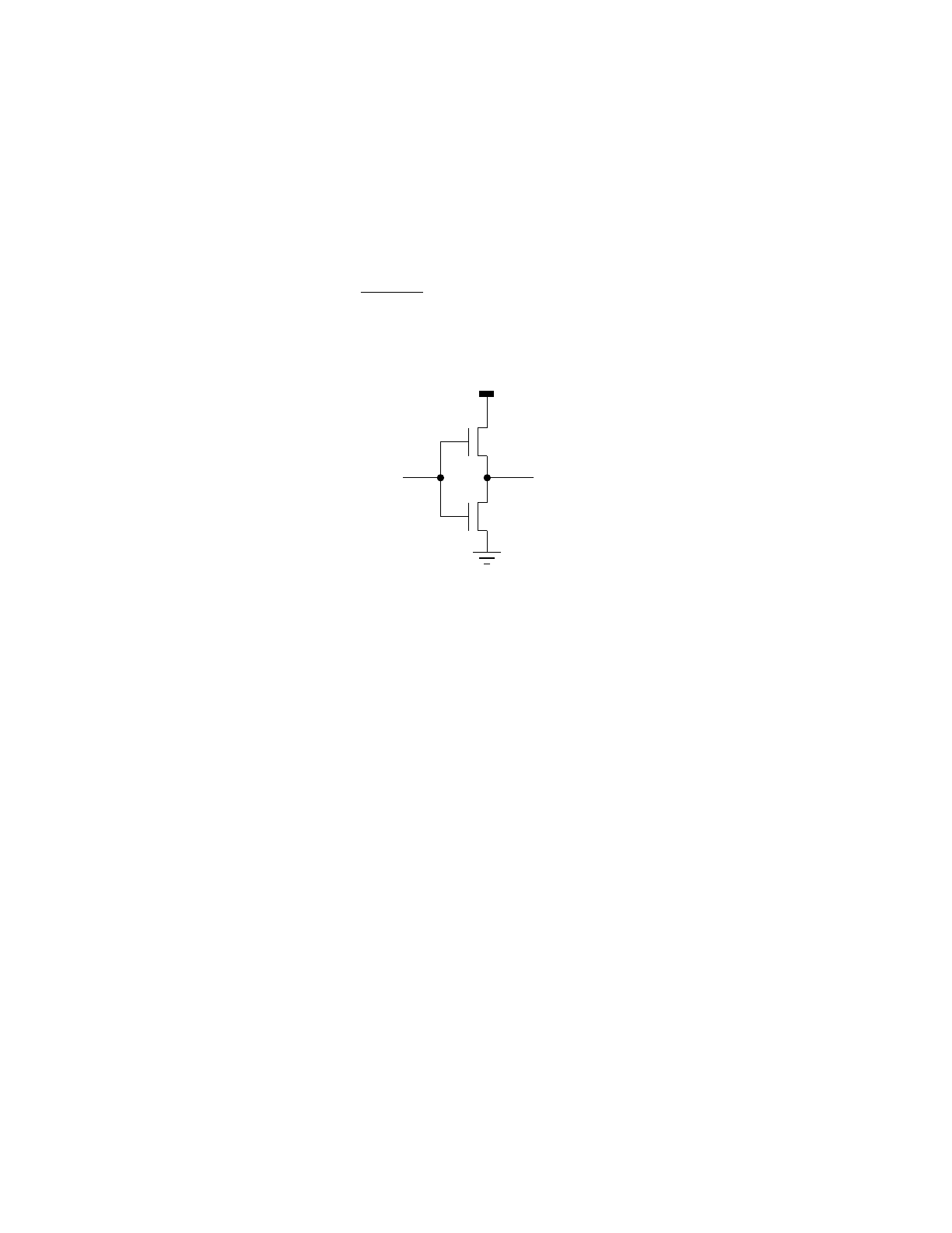
MOTOROLA PINS AND CONNECTIONS M68HC11
2-22 REFERENCE MANUAL
Essentially all current is due to gates that are in the linear region during transitions and
for charging and discharging internal capacitances. Because the input is very high im-
pedance, if it is not connected, the input can oscillate or float to a midsupply level. Ei-
ther of these conditions can result in added power-supply current. The oscillation case
can result in coupling of noise to the power supply. In older CMOS designs, the large
currents caused by an input that floated to midsupply could even induce CMOS latch-
up, which could destroy the integrated circuit. Current design techniques on the
MC68HC11A8 have made latchup due to a floating input unlikely, but it is still impor-
tant to terminate unused inputs to avoid oscillation, noise, and added supply current.
Some inputs on the MCU (RESET, EXTAL, MODA, and MODB) cannot be left unter-
minated in any system.
Figure 2-14 CMOS Inverter
The port E input pins have an extra N-channel device between VSS and the bottom of
the N-channel device of the input inverter. Since this extra device is only enabled for
half a cycle during a digital read of port E, it is less important to terminate unused port
E pins than other unused inputs. In cases of very slow bus frequencies, even half a
cycle might be a significant length of time, and unused port E pins could be terminated.
In some battery-powered systems where port E is read often, it would be desirable to
eliminate the potential added supply current.
Since the VREFL and VREFH pins do not connect to the inputs of any CMOS gates with-
in the MC68HC11A8, these pins do not need terminating if they are not used. Although
termination is not required, it may reduce the risk of damage due to high-voltage static
electricity.
Other than A/D pins, there are two basic types of input pins on the MC68HC11A8 —
an input-only pin and an input/output pin. The best method to terminate unused inputs
is with a pull-up or pulldown resistor for each unused pin. Input-only pins can be con-
nected to each other and then to a common termination point. Although this method is
less expensive and takes less space than individual pull-ups, it is much harder to sep-
arate and use one of these pins if it is needed later. Although input-only pins can be
connected directly to VDD or VSS, it is better not to because this connection makes it
difficult to change the level at that input. If a pull-up or pulldown resistor is used in-
stead, a signal can easily be connected to the input later. The preferred method of ter-
OUT
VDD
P
N
IN

M68HC11 PINS AND CONNECTIONS MOTOROLA
REFERENCE MANUAL 2-23
minating pins that can be configured for input or output is with individual pull-up or
pulldown resistors for each unused pin. Some users leave these pins unconnected
and reconfigure them as outputs during initialization. There is still a brief period during
reset and initialization where these pins are unterminated inputs. There is also a small
risk that a defective system might fail to reconfigure these pins as outputs. A pin ca-
pable of being configured as an output should never be connected to another such pin
or directly to either power-supply rail. If the pin ever became an output, there is a pos-
sibility of high current drain due to an output conflict.
Part of the verification procedure for the design of every MCU system should be a pin-
by-pin review of what is connected to every pin on the MCU to eliminate potential prob-
lems.
2.4 Avoidance of Pin Damage
Any integrated circuit can be damaged or destroyed by exposure to illegal voltages or
conditions. By understanding the failure mechanisms, a designer can protect against
damaging conditions. In some cases, a product can even be designed to tolerate com-
mon end-user errors by designing protective interface circuits.
The data sheets for integrated circuits state conservative limits and conditions that will
definitely protect the integrated circuit. The consequences of violating the specified
limits are not usually discussed because there are too many variables affecting the re-
sults. In some cases, the MCU can tolerate significantly worse conditions than the stat-
ed limits, although it is almost impossible to quantify or guarantee this better
performance for all parts and conditions.
There are several basic types of pin interface circuits on the MC68HC11A8. The exact
devices connected to the pin influence what happens as the voltage level at the pin is
driven above VDD or below VSS. Many other factors, including ambient temperature
and lot-to-lot process variations, also influence the reaction of the MCU to illegal volt-
age levels and conditions. The following discussion explains the conditions leading to
actual damage and what that damage might be. This information should be used as a
guideline to help engineers avoid conditions leading to possible MCU damage.
Connected to the substrate of the silicon die, the VSS pin is the reference point from
which all other voltages are measured. The VDD pin is the main positive power supply
for the MCU. Data sheet information is tested and guaranteed for VDD equal to 5 V ±
10 percent, but, in limited temperature range applications, the MCU can operate over
a wider range of VDD (some timing and drive capability specifications may not be met).
VDD and operating temperature have a significant effect on the speed of CMOS logic.
As VDD is reduced, the maximum crystal frequency must also be reduced. For VDD
equal 5 V ±10 percent, the MC68HC11A8 can operate with a maximum bus frequency
of 2.1 MHz; when VDD is 3 V, the maximum bus frequency is about 1 MHz. At low tem-
peratures, speed increases and power-supply current decreases. The MCU can typi-
cally operate with VDD levels up to 7 V without damaging the MCU, but timing and drive
levels will differ from the specified limits. Also, there may be some adverse effects on
gate oxides from long-term exposure to VDD greater than or equal to 7 V. A battery-
based application could be exposed to VDD greater than 5 V when batteries are new

MOTOROLA PINS AND CONNECTIONS M68HC11
2-24 REFERENCE MANUAL
and still be expected to work properly as the battery voltage slowly decays to some
level well below 5 V. Although the MC68HC11A8 could be used in such an application,
published specifications do not cover this range of VDD.
2.4.1 Zap and Latchup
Zap and latchup are terms familiar to failure analysis engineers that work on CMOS
integrated circuits. Zap refers to damage caused by very high-voltage static-electricity
exposure. Static-electricity (zap) damage usually appears as breakdown of the rela-
tively thin oxide layers that causes leakage or shorts. Often secondary damage occurs
after an initial zap failure causes a short.
Latchup refers to a usually catastrophic condition caused by turning on an unintention-
al, bipolar, silicon-controlled rectifier (SCR). A latchup SCR is formed by N and P re-
gions in the layout of the integrated circuit, which act as the collector, base, and
emitters of unintentional, parasitic transistors. Bulk resistance of silicon in the wells
and substrate act as resistors in the SCR circuit. Application of voltages above VDD or
below VSS, in conjunction with enough current to develop voltage drops across the
parasitic resistors in the unintentional SCR circuit, can cause the SCR to turn on. Once
this SCR is turned on, it can normally only be turned off by removing all power from
the integrated circuit. The on-impedance of the SCR can overheat and destroy the in-
tegrated circuit.
Improvements in layout and processing techniques have made newer HCMOS devic-
es, such as the MC68HC11A8, much less likely to suffer damage from zap and latch-
up. Because of the destructive nature of these mechanisms, it is impossible to test
every device for zap and latchup limits the way timing and drive levels are tested. To
assure product reliability, sample groups of devices are destructively tested.
2.4.2 Protective Interface Circuits
In applications where MCU pins might be exposed to detrimental conditions, protective
interfaces may be needed to protect the MCU from damage. The two main goals of
any protective interface are to prevent high currents from flowing and to prevent illegal
voltage levels at a pin. A low-pass filter can often satisfy both goals. In less common
situations, it may also be necessary to provide diode clamps to prevent high voltages
at some pins. All pins on the M68HC11 have internal inherent diode clamps to VSS,
but only some of the pins include clamps to VDD. The following subsections discuss
the internal circuits for each type MCU pin and note special considerations for the pro-
tection of these pin types.
Usually, the only pins needing protection are those that are exposed to signals from
outside the system. For example, in an automobile engine controller, the sensors for
air and fuel flow are connected to the engine control module and ultimately to MCU
inputs. These signals are prime candidates for protective interfaces because noise or
illegal levels could accidentally be applied through the interface wiring. On the other
hand, any buses and signals wholly contained within the control module probably do
not require any sort of protective interface because there is little chance that these sig-
nals would be exposed to illegal levels. In a few cases, a protective interface can even
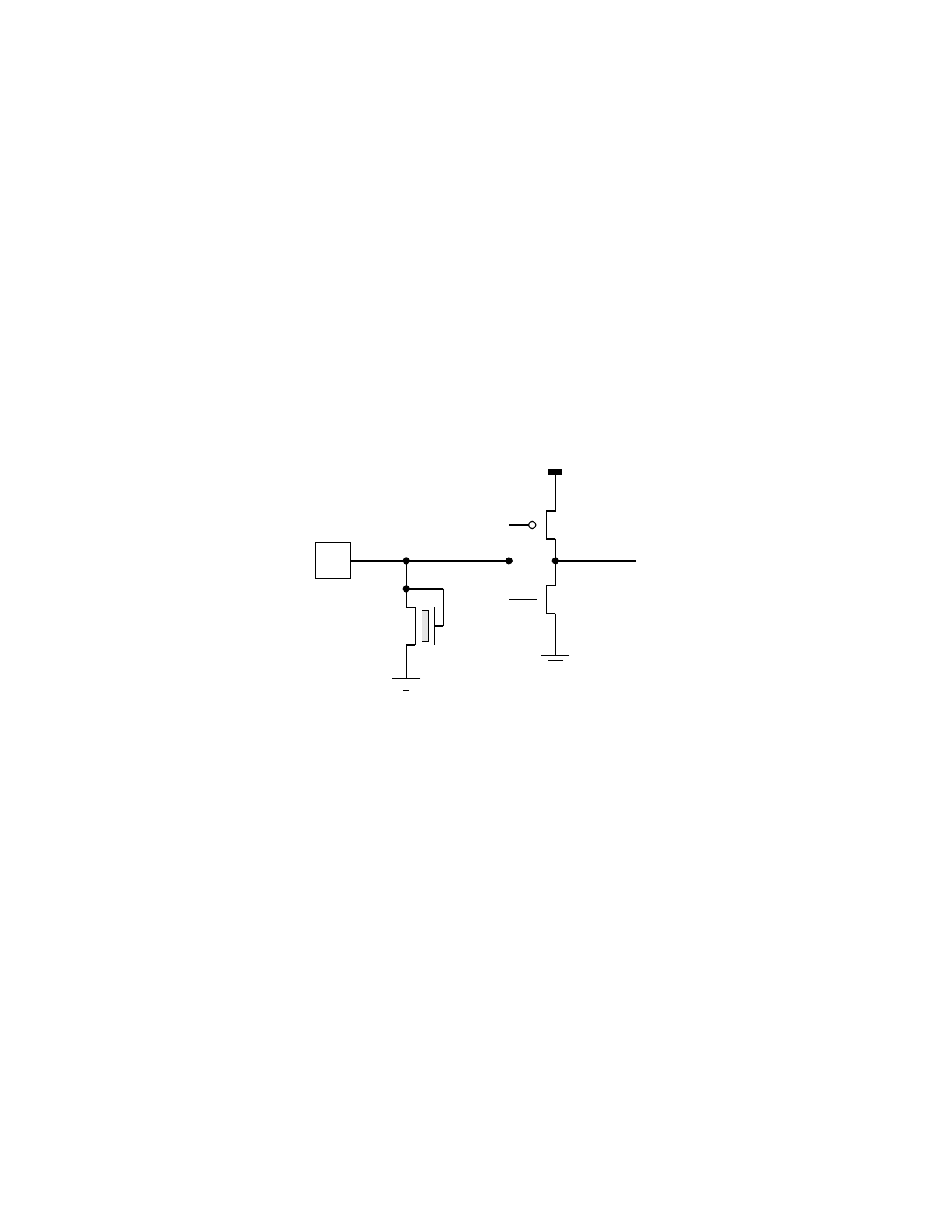
M68HC11 PINS AND CONNECTIONS MOTOROLA
REFERENCE MANUAL 2-25
interfere with normal operation of an MCU signal. For example, a low-pass filter on an
address or data line of an expanded MCU system would introduce significant delays
to these signals, dramatically limiting the maximum operating speed of the system.
2.4.3 Internal Circuitry — Digital Input-Only Pin
Figure 2-15 shows the MOS circuitry for a digital input-only pin. The gates of input
buffer [3] are very high impedance for all voltages that would ever be applied to the
pin. The thick-field protection device [2] normally prevents the pin voltage from reach-
ing levels that could damage the gates of the input buffer. The exact circuitry of the
input buffer may be different for different digital inputs (e.g., to provide hysteresis,
etc.), but only device gates will be connected directly to the pin. Allowing a pin to float
(or be driven) to a midsupply level can result in both the N- and P-channel devices in
the input buffer simultaneously being partially on, which causes excess current and
noise on the VDD/VSS power supply. Port E inputs are exceptions because they are
specifically designed to be driven by analog levels.
Figure 2-15 Internal Circuitry — Digital Input-Only Pin
If a digital input pin (see Figure 2-15) is driven with voltages below VSS, the thick-field
protection device [2] forms an inherent diode junction to VSS, which conducts when the
pin voltage gets more than a diode drop below VSS. As the pin voltage is driven more
negative with respect to VSS, current increases. These currents have a tendency to
influence the die substrate in the area around the protection device, thus affecting the
electrical characteristics of devices in the vicinity. When the pin current is increased to
very high levels (typically more than 100 mA, specified limit is 25 mA), physical dam-
age can result.
As voltage at [1] is driven above VDD, the protection device will begin to conduct and
tend to clamp the input voltage to protect input buffer [3]. The voltage at which this con-
dition will occur varies significantly from lot to lot and over the operating temperature
range. At room temperature, the pin typically does not draw any current until approxi-
mately 20 V; at 125°, the pin may start conducting at a slightly lower level. Up to this
point, the pin appears to function normally and will return a logic one if read. As the pin
P
N
VDD
THICK FIELD
PROTECTION
PIN
N
[1]
[2]
[3]
INPUT
BUFFER

MOTOROLA PINS AND CONNECTIONS M68HC11
2-26 REFERENCE MANUAL
voltage increases, the thick-field protection device begins to conduct more current to
the die substrate, which is VSS. There should be some external series impedance be-
tween the pin and the input voltage source if the MCU will be used in a detrimental
environment. If the input voltage is increased even further, the protection device [2] will
avalanche, and the pin voltage will eventually fold back (typically to about 7 to 12 V).
Under these conditions, a parasitic bipolar transistor, which is not obvious from the
MOS schematic, is turned on and is holding the pin at the 7-volt level. This avalanche
is still normally not destructive to the pin. Since the foldback clamp level is relatively
low impedance, the pin voltage cannot be raised further without supplying a large cur-
rent. If the offending voltage source is increased to increase the pin current, the pin
circuitry will be damaged (specified limit is 25 mA, typically takes more than 100 mA).
Gate oxides in these inputs are not intended to be exposed to voltages above 7 V for
any significant amount of time. With the HCMOS processing used in the
MC68HC11A8, a latchup failure is unlikely unless legal drive limits are grossly exceed-
ed.
2.4.4 Internal Circuitry — Analog Input-Only Pin
Figure 2-16 shows the MOS circuitry associated with an analog input-only pin. This
MOS logic is similar to that for a digital input-only pin except for the addition of the an-
alog multiplexer [5] and the extra N-channel device below the buffer. The N-channel
device [5] acts as an analog multiplexer and affects the behavior of an analog input pin
when exposed to negative voltages. The N-channel device [4] allows the analog input
pins to be driven by intermediate levels without causing the noise and current normally
associated with the input buffer when its input is at a midsupply level. This device is
only turned on for half an E-clock cycle during a digital read of port E. Since the analog
input pins (including the VREF pins) are only connected to N-channel devices and high-
impedance gates, these pins can be driven with levels above VDD without the usual
fear of latchup. This aspect is important because the analog reference supply is typi-
cally independent of the VDD supply for noise isolation reasons.
An analog input pin (see Figure 2-16) responds very much like a digital input to illegal
levels except that negative levels at the pin can affect A/D operations. The analog
functions associated with these pins also present some special challenges to protec-
tive interface circuits. Although the N-channel devices [4] eliminates the need for ex-
ternal pull-up or pulldown resistors on unused port E pins, a conservative designer
would still terminate these pins to help prevent static damage.
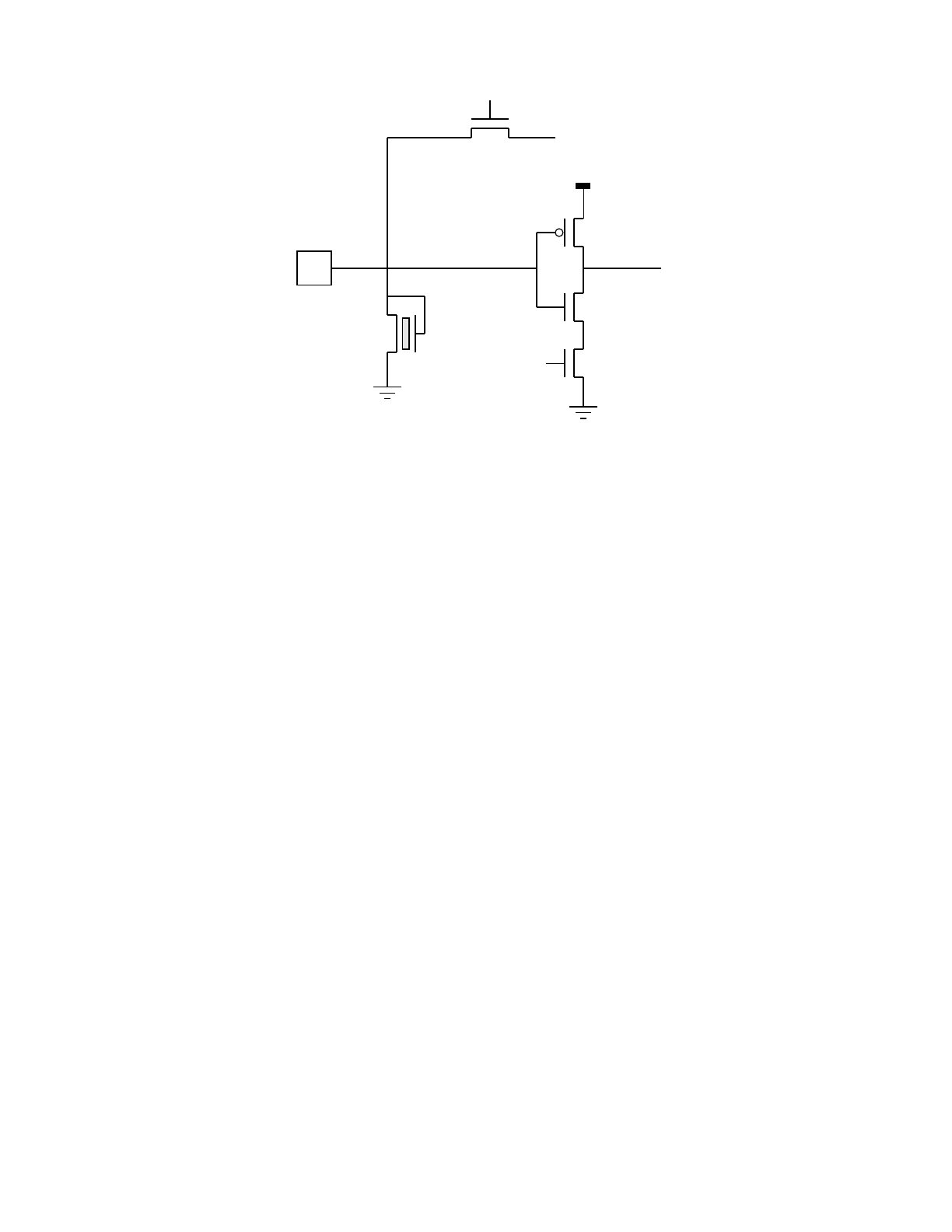
M68HC11 PINS AND CONNECTIONS MOTOROLA
REFERENCE MANUAL 2-27
Figure 2-16 Internal Circuitry — Analog Input-Only Pin
If the pin voltage is driven low enough relative to the gate voltage of the analog multi-
plexer device, this N-channel device can turn on. A conductive path between the neg-
ative pin and the A/D capacitor array may discharge the capacitors and disrupt any A/
D conversion in progress. The thick-field protection device and other circuit and layout
measures around the N-channel multiplexer device are intended to prevent the pin
voltage from becoming negative enough to turn on the multiplexer device. Even with
these internal protective measures, a cautious user should avoid negative levels on
any A/D pin because a large negative transient could still disrupt an A/D conversion.
An A/D conversion can be disrupted in this manner if any A/D pin experiences a seri-
ous negative transient; the transient need not be on the pin associated with the con-
version.
External diode clamps to VDD are not necessarily a good idea on the analog inputs.
Leakage through an external diode would be significant in relationship to the pin leak-
age current; thus, this extra leakage could affect the accuracy of analog conversion
results. Analog input pins can usually be protected by a low-pass filter with enough se-
ries impedance to limit the pin voltage. The amount of series resistance is a trade-off
between a high enough value to limit pin voltage and a low enough value to prevent
pin leakage current from adversely affecting conversion results. Conversion accuracy
is specified for a maximum external series resistance of 10 kΩ. The worst-case spec-
ified leakage current at the pin is 400 nA (at room temperature, leakage is typically
much less). The 400 nA acting through 10 kΩcauses an absolute conversion error of
minus one-fifth of a least significant bit (LSB) when VREF is 5.12 V, leaving only about
one-quarter of an LSB for actual A/D circuit errors before the results would be out of
specified limits. Using a larger external resistance in series with an A/D pin may cause
some inaccuracy due to the leakage current acting through this resistance, but the A/
D will still respond in a predictable manner. There may be valid system design reasons
for choosing a high external series resistance (e.g., to minimize power consumption in
P
N
VDD
THICK FIELD
PROTECTION
PIN
N
[1]
[2]
[3]
INPUT
BUFFER
N
[4]
[5]
ANALOG
MULTIPLEXER
N
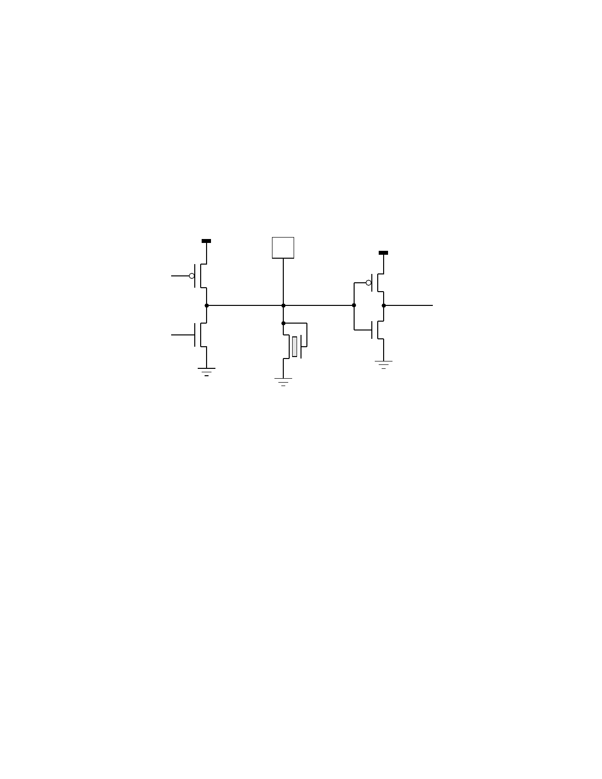
MOTOROLA PINS AND CONNECTIONS M68HC11
2-28 REFERENCE MANUAL
a battery-based system). For additional detailed information concerning the A/D input
pins, see 12.3 A/D Pin Connection Considerations.
2.4.5 Internal Circuitry — Digital I/O Pin
Figure 2-17 shows the MOS circuitry for an MCU pin capable of operating as an input
or an output. Even when the pin is configured to disable the output driver circuitry, the
MOS transistors still affect the way the pin reacts to illegal levels. The P-channel de-
vice of the output driver [3] forms an inherent diode to VDD, and the N-channel device
forms an inherent diode to VSS, which is in parallel with the inherent diode of the thick-
field protection device.
Figure 2-17 Internal Circuitry — Digital I/O Pin
When the pin is configured as a high-impedance input, input signals are clamped to
within a diode drop of the VSS and VDD power-supply rails. When the pin is configured
as an output, the P- or N-channel device provides a low-impedance path to VDD or
VSS, respectively. The current into or out of the pin should be limited to prevent dam-
age. The specified current limit is 25 mA although these pins can typically withstand
transients of more than 100 mA at nominal room temperature.
The port C and port D I/O pins of the M68HC11 can be configured as open-drain-type
outputs. This configuration disables the gate signal to the P-channel device of the out-
put buffer so the pin cannot be driven to an active-high logic level, but the P-channel
device is still physically present and forms an inherent diode to VDD. In a few applica-
tions, the situation will arise where two or more MCU I/O pins are tied to the same
point. Software would be arranged so that no more than one of these I/O pins is con-
figured as an output at any time to avoid output driver contention. In these applications,
the I/O pins should be configured for the open-drain mode so the output drivers are
prevented from high-current contention.
P
N
THICK FIELD
PROTECTION
PIN
N
[1]
[2]
[3]
INPUT
BUFFER
V
DD
N
P
[4]
[5]
OUTPUT
BUFFER
V
DD
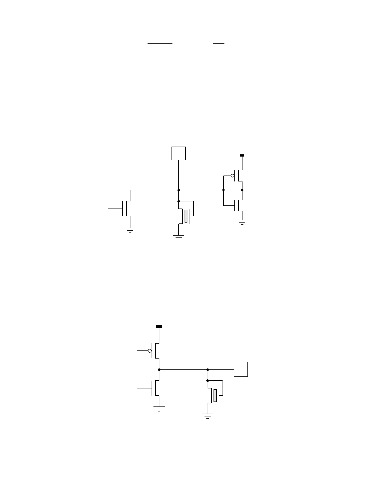
M68HC11 PINS AND CONNECTIONS MOTOROLA
REFERENCE MANUAL 2-29
2.4.6 Internal Circuitry — Input/Open-Drain-Output Pin
Two pins on the M68HC11 (RESET and MODA/LIR) have high-impedance input func-
tions as well as open-drain output functions (see Figure 2-18). These pins are similar
to I/O pins except that there is no P-channel device in the output driver. Since the P-
channel output device is not present, there is no inherent diode to VDD. In terms of
negative illegal levels at these pins, there are two diodes clamping the pin to a diode
drop below ground. In terms of positive levels above VDD, the N-channel output device
starts to conduct before the thick-field protection device; thus, the clamp level for these
pins will typically be lower than that for a digital input-only pin. As for any MCU pin,
current should be limited to prevent damage.
Figure 2-18 Internal Circuitry — Input/Open-Drain-Output Pin
2.4.7 Internal Circuitry — Digital Output-Only Pin
Output-only pins react to illegal levels exactly like I/O pins. Figure 2-19 shows the
MOS circuitry for a digital output-only pin.
Figure 2-19 Internal Circuitry — Output-Only Pin
P
N
THICK FIELD
PROTECTION
PIN
N
[1]
[2]
[3]
INPUT
BUFFER
N[4]
N-CHANNEL ONLY
OUTPUT BUFFER
VDD
THICK FIELD
PROTECTION
PIN
N
VDD
N
P
OUTPUT
BUFFER
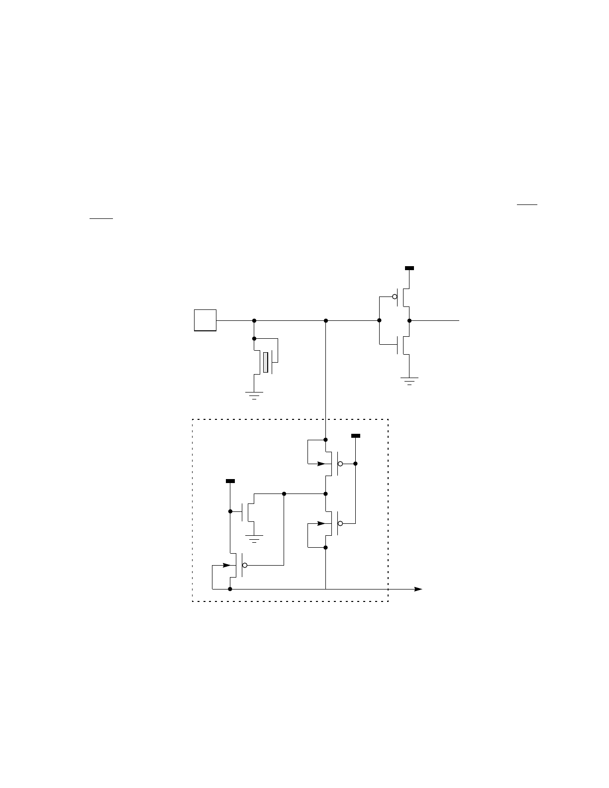
MOTOROLA PINS AND CONNECTIONS M68HC11
2-30 REFERENCE MANUAL
2.4.8 Internal Circuitry — MODB/VSTBY Pin
The MODB/VSTBY pin is unusual because it serves as a standby voltage source in ad-
dition to acting as a mode select input (see Figure 2-20). A MOS switch automatically
connects the internal RAM power supply to the higher of VDD or VSTBY. If an illegal
high level is applied to the MODB/VSTBY pin, this illegal voltage is passed in to the in-
ternal RAM system. A minor elevation of VSTBY relative to VDD can be tolerated during
MCU operation, but any significant elevation can result in incorrect reads of RAM data.
When a battery or other standby voltage source will be used to maintain RAM contents
in the absence of VDD, the MODB/VSTBY pin should be driven by VDD (rather than the
standby source) during normal operation. The MODB/VSTBY pin should not be driven
by a higher level than VDD, except during standby periods; during these periods, RE-
SET should be driven low.
Figure 2-20 Internal Circuitry — MODB/VSTBY Pin
P
N
[3]
INPUT
BUFFER
PIN
[1]
MODB/V
STBY
MOS POWER SWITCH
[4]
[5]
[6]
[7] POWER
TO RAM
VDD
THICK FIELD
PROTECTION
N
[2]
N
V
DD
VDD
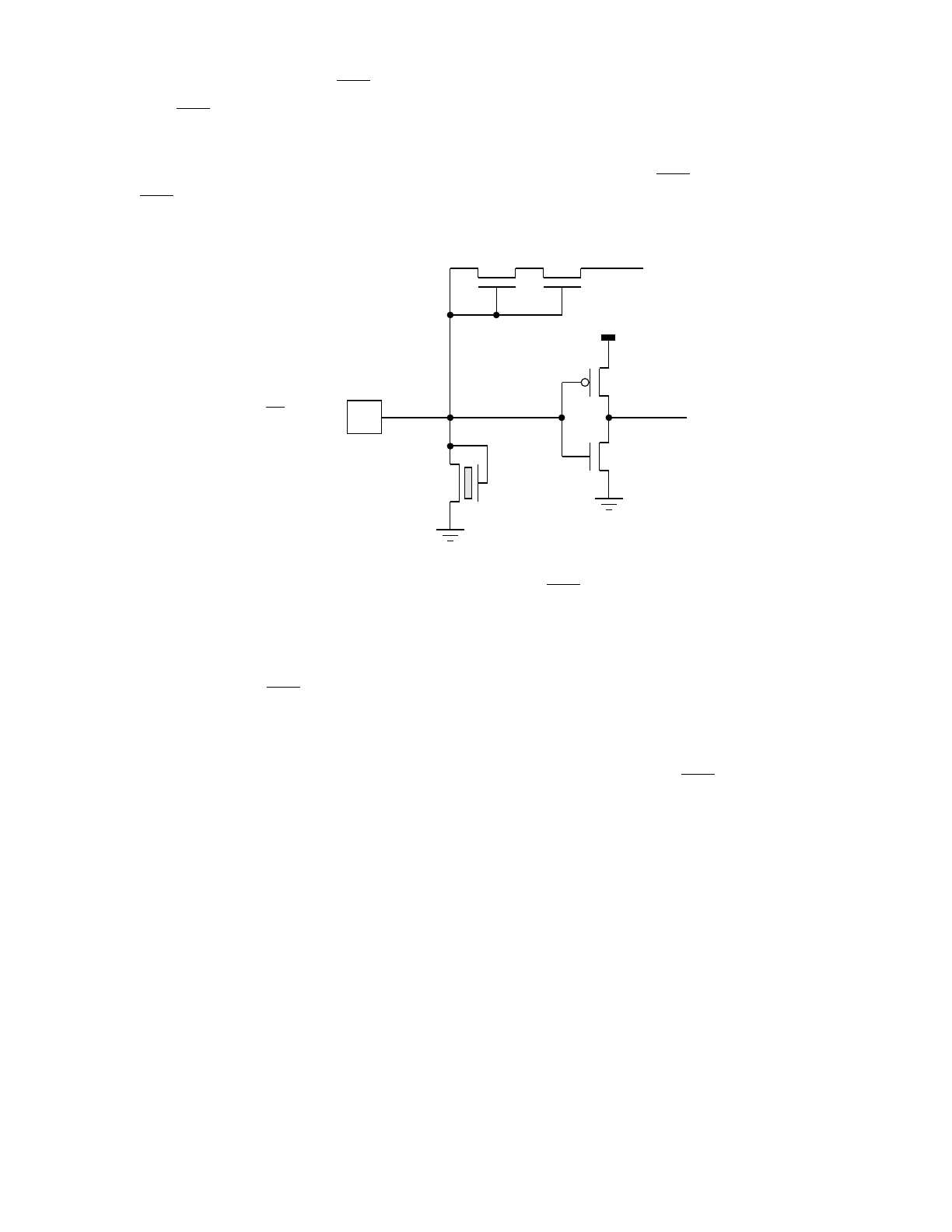
M68HC11 PINS AND CONNECTIONS MOTOROLA
REFERENCE MANUAL 2-31
2.4.9 Internal Circuitry — IRQ/VPPBULK Pin
The IRQ pin is used as a high-voltage (20 V) power source during factory testing. This
high-voltage source supplies power for bulk programming operations because the in-
ternal charge pump is not designed to provide enough current for these bulk program-
ming operations. Figure 2-21 shows the MOS circuitry for the IRQ/VPPBULK pin. The
IRQ/VPPBULK pin essentially reacts like an input-only pin to illegal levels.
Figure 2-21 Internal Circuitry — IRQ/VPPBULK Pin
The normal VPP level used during testing is very near the level where the thick-field
protection device begins to conduct. It is important to limit the current of the VPP power
supply into the IRQ/VPPBULK pin with an external series resistor (typically 27 kΩ) be-
cause noise or overshoot can trigger the low-impedance foldback mechanism of the
protection device. Without a current-limiting resistor, the small metal line connecting
the bonding pad to the pin input circuitry will instantly vaporize. Normal users would
not encounter this potential problem since the VPP function of the IRQ/VPPBULK pin is
only intended for use by Motorola. The current-limiting resistor has no adverse affect
on the bulk programming process since the current requirements for EEPROM pro-
gramming are very small.
2.5 Typical Single-Chip-Mode System Connections
Figure 2-22 is the schematic for a simple single-chip-mode system, which can be op-
erated in normal single-chip or special bootstrap mode. This circuit can be used as the
basis for any single-chip-mode application. In most cases, the circuitry for the power
supply, oscillator, and mode selects can be used exactly as shown in this system. Only
specialized I/O circuitry specific to the application needs to be designed from scratch.
All unused inputs are terminated in an appropriate manner.
P
N
VDD
THICK FIELD
PROTECTION
PIN
N
[1]
[2]
[3]
INPUT
BUFFER
IRQ/V PPBULK
[4]
VPP
NN
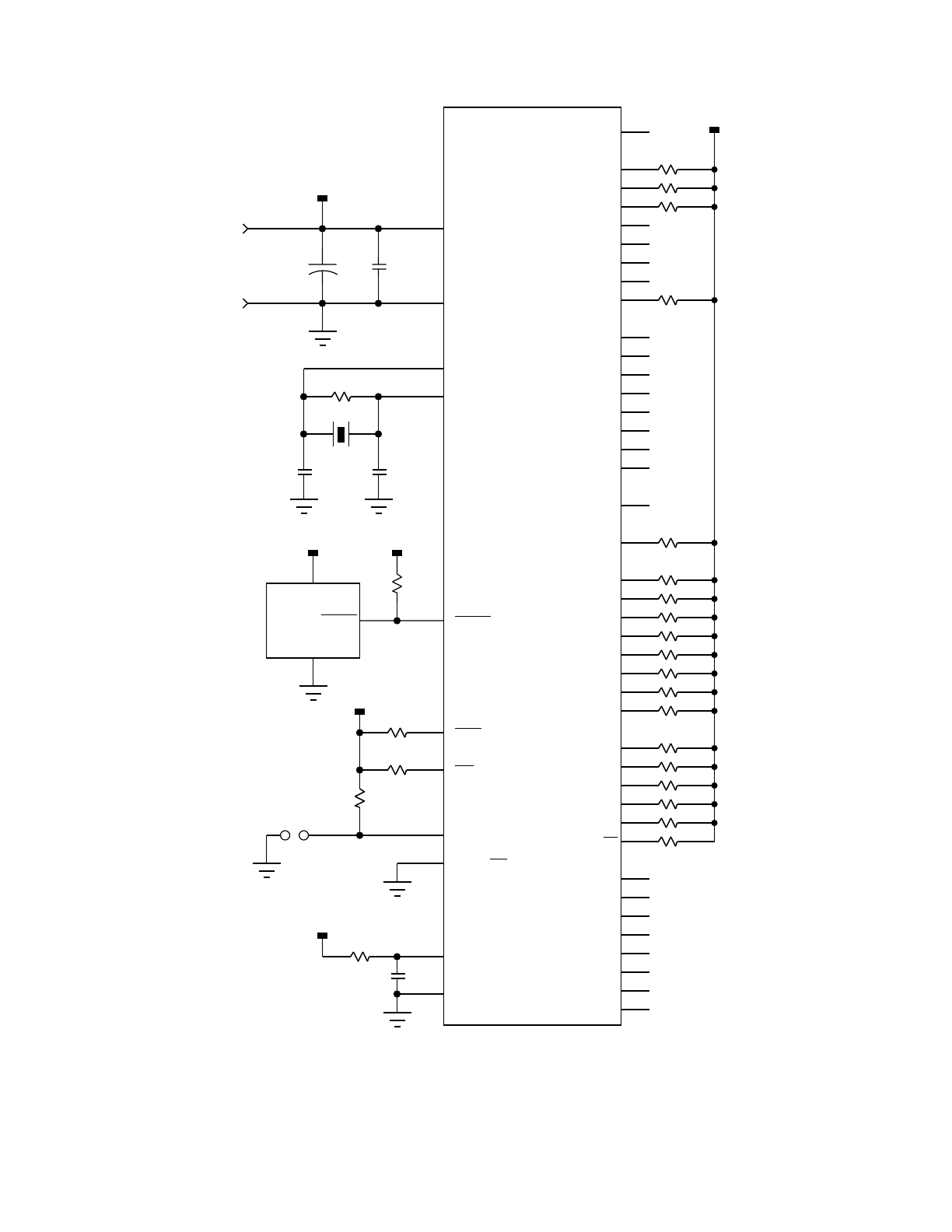
MOTOROLA PINS AND CONNECTIONS M68HC11
2-32 REFERENCE MANUAL
Figure 2-22 Basic Single-Chip-Mode Connections
4.7K
MC34064
RESET
GND
IN
1K
1µF
10M
8.0 MHz
18 pF
18 pF
4.7K
4.7K
0.1 µF
4.7 µF
SYSTEM
POWER
4.7K
CONNECT
JUMPER FOR
BOOTSTRAP MODE
RESET
XIRQ
IRQ
V
V
RH
RL
STBY
MODA/LIR
V
MODB/V
DD
VSS
EXTAL
XTAL
MC68HC11A8
PA0/IC3
PA1/IC2
PA2/IC0
PA3/OC5/OC1
PA4/OC4/OC1
PA5/OC3/OC1
PA6/OC2/OC1
PA7/PAI/OC1
PB0
PB1
PB2
PB3
PB4
PB5
PB6
PB7
STRB
PE4/AN4
STRA
PE5/AN5
PC0
PC1
PC2
PC3
PC4
PC5
PC6
PC7
PE6/AN6
PD0/RxD
PD1/TxD
PD2/MISO
PD3/MOSI
PD4/SCK
PD5/SS
PE7/AN7
PE0/AN0
PE1/AN1
PE2/AN2
PE3/AN3
10K TYP
E
VDD
+
VDD
VDD
VDD
VDD
VDD

M68HC11 PINS AND CONNECTIONS MOTOROLA
REFERENCE MANUAL 2-33
2.6 Typical Expanded-Mode-System Connections
The schematic shown in Figure 2-23 is for a fairly straightforward expanded-mode
system, which can be operated in normal expanded mode or special test mode. This
circuitry can be used as the basis for any expanded-mode application. In most cases,
the circuitry for the power supply, oscillator, and mode selects can be used exactly as
shown in this system. If additional memory or peripheral functions are added to the ad-
dress and data buses, the loading should be reviewed to determine whether or not ad-
ditional buffering is required. Loading is generally limited by load capacitance before
the dc drive capabilities of the MCU drivers are reached. At bus frequencies lower than
2 MHz, more capacitance can be driven before buffers are required. In applications
where heavy bus loading occurs, it is necessary to increase power-supply bypass ca-
pacitors to provide for these higher bus switching demands on VDD.
The address decoding used in this example system is unusual in that the external
EPROM is decoded to appear in either of two memory areas. Some commonly used
terms to describe this type of decoding are partial decode, redundant mapping, and
mirroring. In this system, the external EPROM appears at $E000–$FFFF and at
$A000–$BFFF so that the reset vector can be fetched out of this EPROM whether the
MCU is operating in normal expanded mode or special test mode. This mapping also
allows the MCU to come out of reset in special test mode, check the contents of the
EEPROM-based CONFIG register (change CONFIG if necessary), and then change
the operating mode to normal expanded mode. There are several potential advantag-
es to starting a system this way (see 3.5.3 Special Test Mode).
The 74HC138 decoder provides address-qualified read enable and write enable sig-
nals for two 8-Kbyte by 8 static RAMs. The other four outputs of this 74HC138 provide
additional chip selects for additional RAM or peripheral devices. Since the R/W signal
drives one of the address selects of the 74HC138, there are four active-low read en-
able outputs and four active-low write enable outputs. The timing for these outputs is
controlled by the E clock and the propagation delay through the 74HC138 decoder.
Address and R/W are stable long before the rising edge of the E clock.
The decoding for the EPROM was done with two sections of a quad NAND gate. Ad-
dress valid time controls the chip select access time of the EPROM. This chip select
decode provides for a longer access time than the chip select arrangement on the
RAMs because EPROMs are typically slower than static RAMS. The E clock controls
the output enable of the EPROM, which typically has a much shorter setup time re-
quirement than the chip-select input to the EPROM. Since address line 14 (ADDR14)
is not included in the decode for the EPROM, the EPROM will appear twice in the
memory map: at $A000–$BFFF where ADDR14 is low and at $E000–$FFFF where
ADDR14 is high.
A few potential address conflicts can occur in this system. The on-chip ROM and/or
on-chip EEPROM can conflict with the external EPROM. For the purposes of this ex-
ample, it is assumed that the internal ROM will not be used and will be disabled by the
ROMON control bit in the CONFIG register. The potential for conflict with the EE-
PROM poses no concern in normal expanded mode because the external MCU data
bus is high impedance and ignored during reads of the internal EEPROM. In special

MOTOROLA PINS AND CONNECTIONS M68HC11
2-34 REFERENCE MANUAL
test mode, there is a potential for an undesirable conflict if the EEPROM is read while
the IRV function is enabled (see 2.7.2 Internal Read Visibility (IRV). Although this
conflict would not typically be destructive, it would increase power consumption and
generated noise. In this example system, the special test mode would only be in effect
for a short time after reset, and reads of the internal EEPROM could easily be avoided
during this time.
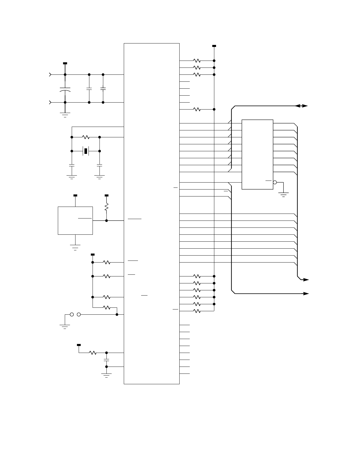
M68HC11 PINS AND CONNECTIONS MOTOROLA
REFERENCE MANUAL 2-35
Figure 2-23 Basic Expanded Mode Connections (Sheet 1 of 2)
VDD
+
4.7K
MC34064
VDD
RESET
VDD
GND
IN
1K
1µF
VDD
10M
8.0 MHz
18 pF
18 pF
VDD
4.7K
4.7K
0.01 µF
10 µF
SYSTEM
POWER
CONNECT
JUMPER FOR
TEST MODE
RESET
XIRQ
IRQ
V
V
RH
RL
MODA/LIR
V
STBY
MODB/V
DD
VSS
EXTAL
XTAL
MC68HC11A8
PA0/IC3
PA1/IC2
PA2/IC0
PA3/OC5/OC1
PA4/OC4/OC1
PA5/OC3/OC1
PA6/OC2/OC1
PA7/PAI/OC1
A8
A9
A10
A11
A12
A13
A14
A15
PE4/AN4
PE5/AN5
PE6/AN6
PD0/RxD
PD1/TxD
PD2/MISO
PD3/MOSI
PD4/SCK
PD5/SS
PE7/AN7
PE0/AN0
PE1/AN1
PE2/AN2
PE3/AN3
VDD
10K TYP
E
4.7K
4.7K
1µF
AS
AD0
AD1
AD2
AD3
AD4
AD5
AD6
AD7
OE
Q0
Q1
Q2
Q3
Q4
Q5
Q6
Q7
LE
D0
D1
D2
D3
D4
D5
D6
D7
74HC373
A0
A1
A2
A3
A4
A5
A6
A7
A8
A9
A10
A11
A12
A13
A14
A15
D0
D1
D2
D3
D4
D5
D6
D7
R/W
E
AS
R/W
CONTROL BUS
DATA BUS
ADDRESS BUS
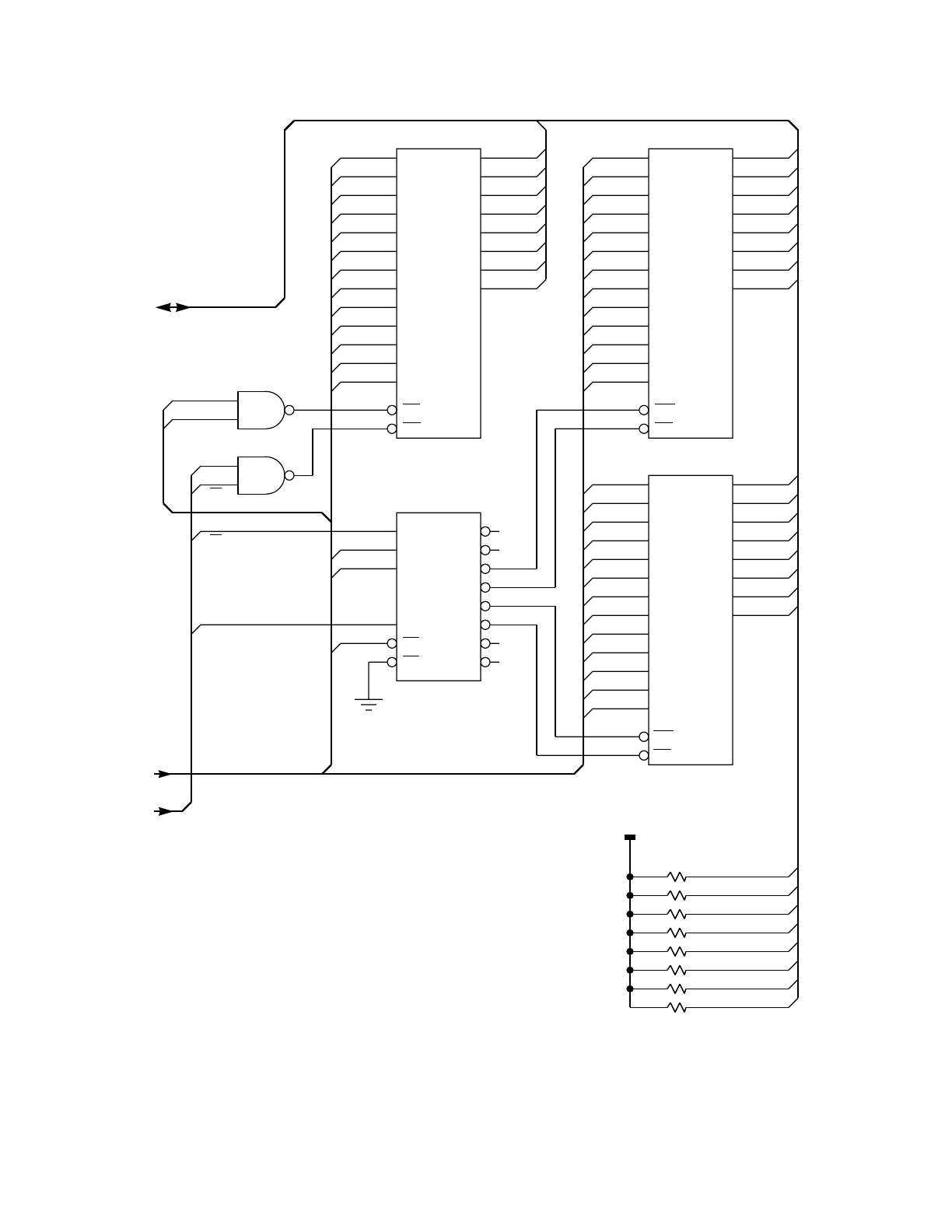
MOTOROLA PINS AND CONNECTIONS M68HC11
2-36 REFERENCE MANUAL
Figure 2-24 Basic Expanded Mode Connections (Sheet 2 of 2)
CONTROL BUS
DATA BUS
ADDRESS BUS
D0
D1
D2
D3
D4
D5
D6
D7
A0
A1
A2
A3
A4
A5
A6
A7
D0
D1
D2
D3
D4
D5
D6
D7
A8
A9
A10
A11
A12
8K X 8 RAM
OE
D0
D1
D2
D3
D4
D5
D6
D7
CS
A0
A1
A2
A3
A4
A5
A6
A7
D0
D1
D2
D3
D4
D5
D6
D7
A8
A9
A10
A11
A12
8K X 8 EPROM
D0
D1
D2
D3
D4
D5
D6
D7
A0
A1
A2
A3
A4
A5
A6
A7
D0
D1
D2
D3
D4
D5
D6
D7
A8
A9
A10
A11
A12
8K X 8 RAM
A0
A1
A2
A3
A4
A5
A6
A7
A8
A9
A10
A11
A12
A0
A1
A2
A3
A4
A5
A6
A7
A8
A9
A10
A11
A12
A0
A1
A2
A3
A4
A5
A6
A7
A8
A9
A10
A11
A12
V
DD
D0
D1
D2
D3
D4
D5
D6
D7
10K TYP
Y0
Y1
Y2
Y3
Y4
Y5
Y6
Y7
A0
A1
A2
G
G1
G2
A14
A15
A13
RD
WE
RD
WE
E
R/W
E
R/W
A15
A13
74HC138

M68HC11 PINS AND CONNECTIONS MOTOROLA
REFERENCE MANUAL 2-37
2.7 System Development and Debug Features
The designers of the M68HC11 carefully considered the system development needs
of the user. Since smaller users cannot afford thousands of dollars for a development
system, the M68HC11 was specifically designed to accommodate low-cost develop-
ment tools. The M68HC11 EVB evaluation board and M68HC11 EVM evaluation mod-
ule are two examples of such low-cost tools. Several customers have also built small
plug-in modules that emulate the MC68HC11A8 for product development purposes.
The small size of these plug-in emulators is possible because of the development fea-
tures designed into the M68HC11.
2.7.1 Load Instruction Register (LIR)
The LIR signal is intended as a debugging aid. This signal is driven to active low for
the first bus cycle of each new instruction, making it easy to reverse assemble (disas-
semble) instructions from the display of a logic analyzer.
2.7.2 Internal Read Visibility (IRV)
During debugging of an application, it is useful to see what is being read from internal
registers and memory locations. The IRV feature provides this capability. This feature
should usually be disabled during normal operation of the system due to the possibility
of bus conflicts.
The IRV feature is controlled by the IRV bit in the HPRIO register. When the IRV bit is
one, the data from a read of an internal register or memory location is driven out on
the data bus so it can be monitored by a logic analyzer. If the IRV bit is zero, the IRV
function is disabled, and the data bus is undriven during reads of an internal address.
Special restrictions apply to the use of the IRV bit and function. When the MCU is reset
in normal modes, the IRV bit is initially zero. In all but the newest derivatives in the
M68HC11 Family, the IRV bit may not be written to one in the normal modes. In special
test and bootstrap modes, the IRV bit is initially one and may be written to zero after
which it becomes a read-only bit.
Care should be used if the IRV function is enabled. During reads of an internal ad-
dress, the data bus is driven out even though the R/W line indicates that the bus direc-
tion is toward the MCU. Some external device may also be trying to drive the data
lines, which leads to an undesirable bus contention. In a test or debugging situation,
special address decode logic can be used to prevent such contention. It would be ex-
pensive and inappropriate to have this additional decode logic on all normal mode sys-
tems; thus, the IRV function was only provided in the special test and bootstrap
modes. Due to several customer requests for the IRV function in normal modes, the
logic was changed to allow the function to be enabled in normal modes on new ver-
sions of the M68HC11. The default condition in normal modes is still IRV equals zero,
which disables the function. If a user specifically wants the IRV function, IRV may be
written to one, and the user becomes responsible for avoiding bus contentions. IRV
can be written to one at any time unless it has previously been written to zero. If the
IRV bit is written to zero, the function becomes disabled until the next reset sequence.

MOTOROLA PINS AND CONNECTIONS M68HC11
2-38 REFERENCE MANUAL
2.7.3 MC68HC24 Port Replacement Unit
The MC68HC24 PRU is a gate array that emulates the single-chip mode functions of
ports B and C, which are lost to the expansion bus function when the MCU is operated
in expanded modes. The expanded mode permits program development in an exter-
nal EPROM. A system consisting of an M68HC11 in expanded mode, an MC68HC24,
an HC373 octal latch, and an external EPROM performs like the MC68HC11A8 oper-
ating in single-chip modes, thus allowing an application program to be developed and
tested before a masked ROM pattern is ordered.
The logic in the M68HC11 was specifically designed to permit emulation of single-chip
functions with the MC68HC24. First, the addresses associated with ports B and C and
their handshake I/O functions are treated as external addresses when the MCU is op-
erating in expanded modes. Next, the interrupts associated with the handshake I/O
system are vectored to the same address as IRQ interrupts. Thus, the interrupt output
of the MC68HC24 can be connected to the IRQ interrupt input of the MCU, and hand-
shake interrupts will be treated the same as internal handshake functions. The
M68HC11 allows registers and/or internal RAM to be remapped to any 4-Kbyte bound-
ary. The MC68HC24 copies this logic so that the registers in the MC68HC24 will au-
tomatically track the internal remapping logic. Software written on an expanded
system, including an MC68HC24, will operate exactly as it would in the internal ROM
of an MC68HC11A8 in single-chip mode.

M68HC11 CONFIGURATION AND MODES OF OPERATION MOTOROLA
REFERENCE MANUAL 3-1
SECTION 3
CONFIGURATION AND MODES OF OPERATION
This section discusses the mechanisms that allow the MC68HC11A8 to conform to a
wide variety of applications. These mechanisms include hardware mode selection cir-
cuitry, a nonvolatile EEPROM-based configuration register, and protected control reg-
ister bits. The majority of the control bits in the MC68HC11A8 are accessible at any
time by software and will be discussed throughout this manual.
The term mode is used in more than one context in discussing the microcontroller unit
(MCU). For example, the serial peripheral interface (SPI) is said to be in either the
master or slave mode, the parallel I/O system is said to be in simple strobed mode,
full-input handshake mode, or full-output handshake mode. In most cases, there is no
confusion about what the term mode refers to; however, the use of the term mode in
conjunction with STOP and WAIT is often misunderstood. STOP and WAIT are actu-
ally modes of operation of the central processing unit (CPU) as opposed to single-chip
and expanded modes, which are modes of operation of the MCU integrated circuit. In
this section, the MCU operating modes and other mechanisms controlling the basic
configuration of the MCU are discussed.
Very few MCU functions are influenced by the mode of operation. For example, the
timers, analog-to-digital converter (A/D), and serial I/O functions all work the same in
expanded modes as they do in single-chip modes. The parallel I/O functions of 18 pins
are lost in the expanded modes but can be regained with a special, external, port-re-
placement chip called the MC68HC24. In the two special modes of MCU operation,
some special testing functions become accessible, including the ability for software to
change the MCU mode.
3.1 Hardware Mode Selection
There are only two fundamental modes of operation for the MC68HC11A8 MCU: sin-
gle chip and expanded. Each mode has a normal variation and a special variation.
These four mode variations are selected by the levels on the mode A (MODA) and
mode B (MODB) pins during reset. The special variation of single-chip mode is called
special bootstrap mode; the special variation of the expanded mode is called special
test mode. The special bootstrap mode allows programs to be downloaded through
the on-chip serial communications interface (SCI) into internal random-access mem-
ory (RAM) to be executed. The bootloaded program is used for a variety of tasks such
as loading calibration values into internal electrically erasable programmable read-
only memory (EEPROM) or performing diagnostics on a finished module. The boot-
strap mode is a special user’s mode, not a factory test mode. The special test mode,
which is intended primarily for factory testing, is seldom used by the user except for
emulation, development, or in other rare circumstances.
MOTOROLA CONFIGURATION AND MODES OF OPERATION M68HC11
3-2 REFERENCE MANUAL
3.1.1 Hardware Mode Select Pins
The hardware mode select mechanism starts with the logic levels on the MODA and
MODB pins while the MCU is in the reset state. The logic levels on the MODA and
MODB pins are fed into the MCU by way of a clocked pipeline path. The levels cap-
tured are those that were present part of a clock cycle before the RESET pin rose,
which assures there will be a zero hold-time requirement on the mode select pins rel-
ative to the rising edge at the RESET pin. The captured levels determine the logic state
of the special mode (SMOD) and mode A select (MDA) control bits in the highest pri-
ority interrupt (HPRIO) register. These two control bits actually control the logic circuits
involved in hardware mode selection. Table 3-1 summarizes the operation of the
mode pins and mode control bits.
After RESET rises, the mode select pins no longer influence the MCU operating mode.
The MODA pin serves the alternate function of load instruction register (LIR) when the
MCU is not in reset. The open-drain active-low LIR output pin drives low during the first
E-clock cycle of each instruction. The MODB pin serves the alternate function of a
standby power supply (VSTBY) to maintain RAM contents when VDD is not present.
The power-saving mode, STOP, is an alternate way to save RAM contents, which
does not require a separate standby power source.
3.1.2 Mode Control Bits in the HPRIO Register
The following register and paragraphs show the HPRIO register. The four low-order
bits (PSEL[3:0]) are not related to the mode select logic and will be discussed in SEC-
TION 5 RESETS AND INTERRUPTS. The HPRIO register may be read at any time,
but the four high-order bits may only be written under special circumstances. Usually,
control bits for unrelated on-chip systems would not be mixed in the same register.
RBOOT — Read Bootstrap ROM
Can be written only while SMOD equals one
1 = Bootstrap ROM enabled at $BF40–$BFFF
0 = Bootstrap ROM disabled and not present in memory map
The RBOOT control bit enables or disables the special bootstrap control ROM. This
Table 3-1 Hardware Mode Select Summary
Inputs Mode Description Control Bits in HPRIO (Latched at Reset)
MODB MODA RBOOT SMOD MDA IRV
1 0 Normal Single Chip 0000
1 1 Normal Expanded 0010
0 0 Special Bootstrap 1101
0 1 Special Test 0111
HPRIO — Highest Priority I-Bit Interrupt and Miscellaneous $103C
BIT 7 654321BIT 0
RBOOT SMOD MDA IRV PSEL3 PSEL2 PSEL1 PSEL0
RESET: (Refer to Table 3-1)

M68HC11 CONFIGURATION AND MODES OF OPERATION MOTOROLA
REFERENCE MANUAL 3-3
192-byte, mask-programmed ROM contains the firmware required to load a user’s
program through the SCI into the internal RAM and jump to the loaded program. In all
modes other than the special bootstrap mode, this ROM is disabled and does not oc-
cupy any space in the 64 Kbyte memory map. Although it is zero when the MCU
comes out of reset in test mode, the RBOOT bit may be written to one while in special
test mode.
SMOD — Special Mode
May be written to zero but not back to one
1 = Special mode variation in effect
0 = Normal mode variation in effect
MDA — Mode A Select
Can be written only while SMOD equals one
1 = Normal expanded or special test mode in effect
0 = Normal single-chip or special bootstrap mode in effect
IRV — Internal Read Visibility
Can be written only while SMOD equals one; forced to zero if SMOD equals zero
1 = Data driven onto external bus during internal reads
0 = Data from internal reads not visible on expansion bus (levels on bus ignored)
The IRV control bit is used during factory testing and sometimes during emulation to
allow internal read accesses to be visible on the external data bus. Care is required to
avoid data bus contention while IRV is active because the bidirectional data bus is driv-
en out during reads of internal addresses, even though the R/W line suggests the data
bus is in the high-impedance read mode. In normal modes, this function is disabled;
thus, complex decode logic is not required to protect against accidental bus conflicts.
3.2 EEPROM-Based CONFIG Register
The nonvolatile configuration (CONFIG) register allows additional flexibility in the MCU
that would otherwise be provided by a more complex hardware mode select structure.
By using EEPROM to implement the CONFIG register, these system controls are re-
tained even when no power is applied to the MCU. The functions controlled by this reg-
ister are characteristics that must be inherently known to the MCU system as it comes
out of the reset state. Ordinary software-accessible control bits would not effectively
regulate these controls.
3.2.1 Operation of CONFIG Mechanism
The CONFIG register actually consists of an EEPROM byte (separate from the 512-
byte EEPROM array), a static register that holds the configuration information during
operation, and the associated logic, which controls the transfer of information from the
EEPROM byte to the working static register. Programming and erasure of this register
use the same logic used for programming and erasure of the 512-byte EEPROM ar-
ray. Reads of this register return the contents of the static working register, not the EE-
PROM byte. During any reset, the contents of the EEPROM byte are transferred to the
working static register over the data bus. Due to this mechanism, changes to the EE-
PROM CONFIG location are not visible and do not alter the operation of the MCU until

MOTOROLA CONFIGURATION AND MODES OF OPERATION M68HC11
3-4 REFERENCE MANUAL
after a subsequent reset.
Some versions of the M68HC11 Family allow the CONFIG working register to be writ-
ten directly as a normal control register while operating in the special mode variations.
This capability is included primarily to accelerate product testing but could be useful to
the user in some applications. In versions that have this ability, the MCU could be reset
in one of the special modes. The CONFIG register could be checked or written to any
desired value; then the mode could be written to a normal mode to re-enable system-
protection mechanisms. This procedure is independent of the EEPROM byte and the
transfer during reset. Only some versions of the M68HC11 offer this capability. Risk
factors are associated with operating in a special mode; therefore, keep the time be-
tween reset and writing the mode control bits back to a normal mode as short as pos-
sible to minimize these risks.
3.2.2 The CONFIG Register
The CONFIG register is an unusual control register used to enable or disable ROM,
EEPROM, the computer operating properly (COP) watchdog system, and, optionally,
the EEPROM security feature of the MCU. Unlike ordinary control registers, CONFIG
retains its contents even when there is no power applied to the MCU. The contents are
retained when the MCU is completely removed from a system (e.g., when shipped
from the Motorola factory). In this way, the control bits in the CONFIG register are like
mask-programmed options. Unlike mask options, the contents of this register can be
altered after the MCU is manufactured to meet the customer’s specific requirements.
The CONFIG register is read like any other memory location. The contents of the work-
ing static register are returned on such reads as previously described. The CONFIG
register is erased and programmed like an EEPROM location rather than being written
as other registers. The programming and erase operations alter the EEPROM byte,
which does not alter the operation of the MCU until after a subsequent reset operation.
The programming and erase procedures, which are the same as those used to pro-
gram EEPROM locations, use the PPROG register and are discussed in 4.3 EE-
PROM.
The following register and paragraphs describe the CONFIG register and control bits
of the MC68HC11A8. For specific information about the CONFIG register of other
M68HC11 Family members, refer to the technical summary for that member.
NOSEC — EEPROM Security Disabled
A special security feature is available on the MC68HC11A8 if it is requested at the time
a user submits a mask ROM pattern. Once this feature is enabled at the mask-pro-
gramming level, the user activates it by programming the NOSEC bit to zero. While
NOSEC is zero, the MCU can only be reset in single-chip modes (normal single chip
CONFIG — System Configuration $103F
BIT 7 654321BIT 0
0000NOSEC NOCOP ROMON EEON
RESET: 0000See3.2.1 Operation of CONFIG Mechanism

M68HC11 CONFIGURATION AND MODES OF OPERATION MOTOROLA
REFERENCE MANUAL 3-5
or special bootstrap). This restriction is accomplished by forcing the MDA control bit to
zero rather than allowing it to follow the MODA pin level at the rising edge of RESET.
By disallowing expanded modes, a software pirate is prevented from seeing the data
in EEPROM or RAM because there is no external address/data bus in single-chip
modes.
The software pirate can see what is in the on-chip ROM by disabling the security op-
tion, which can only be accomplished after the contents of EEPROM and RAM have
been erased. When a secured part is reset in bootstrap mode, the firmware in the
small bootloader program will not proceed with bootloading until the EEPROM, RAM,
and CONFIG register have been successfully erased. When a secured part is operat-
ed in normal single-chip mode, the user’s program in ROM is responsible for keeping
the MCU secured. The CONFIG register in current versions of the MC68HC11A8 can-
not be altered except in special bootstrap and special test modes.
NOCOP — COP Watchdog System Disabled
The default erased state of this bit corresponds to COP system off.
1 = The COP system is disabled and does not generate system resets.
0 = The COP system is enabled as the MCU comes out of reset.
A software service mechanism must be periodically completed prior to COP time-out
to avoid a system reset. This service will only occur at the proper repeating rate if the
software is executing in the expected, orderly fashion. If a software failure occurs, the
watchdog will time out and will generate a system reset to force the MCU to return to
proper operation. The COP watchdog mechanism is discussed in detail in SECTION
5 RESETS AND INTERRUPTS.
ROMON — Enable On-Chip ROM
The default erased state of this bit corresponds to ROM enabled.
1 = The 8-Kbyte on-chip program memory is enabled.
0 = The 8-Kbyte ROM is disabled and takes no space in the memory map.
In the normal single-chip operating mode, this control bit is overridden so that ROM is
always enabled. In expanded modes, turning off the ROM with this bit allows the reset
and interrupt vectors to be fetched from external memories; therefore, the user need
not know where vectors should point at the time the MCU is manufactured.
EEON — Enable On-Chip EEPROM
The default erased state of this bit corresponds to EEPROM enabled.
1 = The 512-byte on-chip EEPROM memory enabled at locations $B600–$B7FF.
0 = The 512-byte EEPROM is disabled and takes no space in the memory map.
Some versions of the M68HC11 Family have additional control bits in this register. For
example, the MC68HC811A2 uses the upper four bits to remap its 2-Kbyte EEPROM
to the upper half of any 4-Kbyte page of memory. This reference manual is based pri-
marily on the MC68HC11A8; specific information about other family members can be
found in the technical summaries.
The erased state of CONFIG is $0F on an MC68HC11A8. The MC68HC11A1 is the
same die as the MC68HC11A8 but comes from the factory with $0D in CONFIG to dis-
able the internal 8-Kbyte masked ROM. Similarly, the MC68HC11A0 version of the
part comes with $0C in CONFIG to disable both the 8-Kbyte ROM and 512-byte EE-
PROM. The CONFIG byte is not part of the 512-byte EEPROM. If the CONFIG register

MOTOROLA CONFIGURATION AND MODES OF OPERATION M68HC11
3-6 REFERENCE MANUAL
of an MC68HC11A1 or MC68HC11A0 device is erased to $0F, the internal ROM and
EEPROM memories become enabled but are not necessarily useful. The ROM of an
MC68HC11A1 or MC68HC11A0 part may contain a customer’s program (with their
permission) or a defective program. The EEPROM of an MC68HC11A0 part could be
partially/completely broken and should not be used because the error could be related
to temperature or voltage. Therefore, the EEPROM might check as flawless but later
fail when least expected. The upper four bits are not implemented in the working static
register and always read zero. Although the corresponding bits in the EEPROM byte
are implemented, they are not visible to the user.
The erased state of the CONFIG register in the MC68HC811A2 version is $FF, which
means the 2-Kbyte EEPROM is enabled in the area from $F800–$FFFF when the part
comes from the Motorola factory. To use the part, the user must have a meaningful
reset vector at $FFFE,FFFF or must connect the mode pins so the system will come
out of reset in one of the special modes. The reset vector can be programmed into the
internal EEPROM before installing the part into a finished system, or the EEPROM can
be moved out of the way (by programming the CONFIG register) so an external mem-
ory in the end system can provide the reset vector.
3.3 Protected Control Register Bits
In the MC68HC11A8, several sensitive control registers and bits are protected against
writes except under special circumstances. The protect mechanisms include the ability
to write these bits only within the first 64 bus cycles after any reset and/or the ability to
write them only one time after each reset. These bits control the basic configuration of
the MCU where an accidental write could cause serious system problems — that is,
these protections make it practical to include software-controlled features that might
otherwise be excluded. As new members of the M68HC11 Family are developed, ad-
ditional control bits could fall into this category, but in the MC68HC11A8, only three
control registers are involved (INIT, TMSK2, and OPTION). Some users have ex-
pressed concern about being able to write all of these control bits within 64 cycles,
which will not be a problem since only three writes are required.
Because these protect mechanisms are overridden in the special operating modes,
these bits may be changed repeatedly during testing without going through a reset se-
quence. If the MCU is going to be changed to a normal mode variation after being reset
in a special mode, write to the protected registers before writing the SMOD control bit
to zero.
3.3.1 RAM and I/O Mapping Register (INIT)
RAM[3:0] — RAM Map Position
These four bits, which specify the upper hexadecimal digit of the RAM address, control
INIT — RAM and I/O Mapping Register $103D
BIT 7 654321BIT 0
RAM3 RAM2 RAM1 RAM0 REG3 REG2 REG1 REG0
RESET: 00000001

M68HC11 CONFIGURATION AND MODES OF OPERATION MOTOROLA
REFERENCE MANUAL 3-7
the position of the RAM in the memory map. By changing these bits, the RAM can be
repositioned to the beginning of any 4-Kbyte page in the memory map. After reset,
these bits are zeros ($0); thus, the RAM is initially positioned from $0000–$00FF. If
these four bits are written to ones ($F), the RAM moves to $F000–$F0FF. The follow-
ing explanation of the INIT register discusses what happens when RAM or registers
are mapped to the same area of memory as some other internal resource.
REG[3:0] — 64-Byte Register Block Position
These four bits, which specify the upper hexadecimal digit of the address for the 64-
byte block of internal registers, control the position of these registers in the memory
map. By changing these bits, the register block is repositioned to the beginning of any
4-Kbyte page in the memory map. After reset, these bits are 0001 ($1); therefore, the
registers are initially positioned from $1000–$103F. If these four bits are written to
ones ($F), the registers move to $F000–$F03F. The following explanation discusses
what happens when RAM or registers are mapped to the same area of memory as
some other internal resource.
The INIT register allows software to reposition the internal 256-byte RAM and/or 64-
byte register space to any 4-Kbyte page boundary in the 64-Kbyte memory map.
There are two main reasons a user might want this capability. First, this capability al-
lows the user to position RAM, I/O registers, or both in the direct addressing mode
range ($0000–$00FF). Instructions that use the direct addressing mode assume the
upper eight bits of the address are $00; thus, these instructions take up less program
memory space and operate faster than the equivalent extended addressing mode in-
structions. The second reason for remapping RAM or registers would be to make the
MCU compatible with the memory map of an existing system. For example, the
MC6801 MCU is not compatible with the Motorola EXORciser. The MDOSdisk-
operating system software requires RAM to exist from $0000–$7FFF, ROM routines
to exist from $E800–$EBFF, and system I/O devices to exist from $EC00–$F000. Be-
cause the MC6801 MCU has internal RAM and registers in $0000–$00FF that cannot
be disabled or moved, it cannot be made compatible with the EXORciser. However,
the MC68HC11A8 can disable its internal ROM with the CONFIG register, and the
RAM and registers can be remapped to $D000 and $C000, respectively, by writing
$DC to the INIT register. This procedure makes the MC68HC11A8 compatible with the
EXORciser system without requiring changes to the existing MDOS software. A vari-
ation on this second reason for remapping RAM and registers would be to make max-
imum use of an external 32-Kbyte RAM in the lower half of the memory map.
Users not needing this capability can leave the RAM and I/O registers in their default
locations ($0000–$00FF for RAM and $1000–$103F for registers). Since the INIT reg-
ister becomes write protected shortly after reset, the user need not worry about acci-
dental changes due to a software error.
The internal address decode circuitry automatically protects against conflicts among
internal resources or between an internal and external resource. When an internal re-
source is read, the external data bus is ignored (even if some external device tries to
drive the data bus) so the CPU will read valid data. If the internal RAM and/or I/O reg-
ister spaces are remapped so an overlap occurs between RAM, register space, or
ROM, priority logic disables all but the highest priority resource. For example, consider

MOTOROLA CONFIGURATION AND MODES OF OPERATION M68HC11
3-8 REFERENCE MANUAL
the case of an expanded mode system where ROM is enabled and both RAM and reg-
isters have been remapped to $F000. For accesses from $F000–$F03F, ROM and
RAM are disabled, and registers have highest access priority. From $F040–$F0FF,
ROM is disabled, and RAM has access priority.
Some users have questions about the priority of access for unused register locations
in the 64-byte register space or the priority of registers in an external MC68HC24. In
the previous example, $F035 would correspond to an unused location in the 64-byte
register space (the register block was moved from its usual position of $1000–$103F
such that it overlaps RAM and ROM at $F000). Reads of this address access the un-
driven internal data bus, and any data present on the data bus pins is ignored. Six lo-
cations in the 64-byte register space become external accesses when the
MC68HC11A8 is operating in an expanded mode. This process allows the MC68HC24
to properly emulate the internal parallel I/O functions associated with the 18 MCU pins,
which are dedicated to the multiplexed expansion bus. Again referring to the earlier
example, if any of these six addresses are accessed, the internal ROM and RAM are
disabled so the CPU gets valid data from the external MC68HC24, which is consid-
ered a part of the internal register space. The six locations of interest are $x002–$x007
(PIOC, PORTC, PORTB, PORTCL, one reserved location, and DDRC). Although x is
usually one, it was changed to $F by software in this example.
3.3.2 Protected Control Bits in the TMSK2 Register
The following register diagram and paragraphs describe the time-protected timer pres-
cale select bits (PR[1:0]) in the timer mask register 2 (TMSK2). The upper four bits of
this register, which are related to the timer and pulse accumulator subsystems, will be
discussed in SECTION 10 MAIN TIMER AND REAL-TIME INTERRUPT and SEC-
TION 11 PULSE ACCUMULATOR. Bits 3 and 2 are not implemented and always read
as zeros.
PR[1:0] — Timer Prescaler Select
These two bits select the prescale rate for the main 16-bit free-running timer system.
The following table shows the relationship between the prescale factor and the value
of these control bits. A prescale factor of one corresponds to a timer count rate of E
clock divided by one; a prescale factor of 16 corresponds to a timer count rate of E
clock divided by 16. In normal modes, this prescale rate can only be changed once
within the first 64 bus cycles after reset, and the resulting count rate stays in effect until
the next reset.
TMSK2 — Timer Mask Register 2 $1024
BIT 7 654321BIT 0
TOI RTII PAOVI PAII 0 0 PR1 PR0
RESET: 00000000
M68HC11 CONFIGURATION AND MODES OF OPERATION MOTOROLA
REFERENCE MANUAL 3-9
3.3.3 Protected Control Bits in the OPTION Register
The following register and paragraphs discuss the time-protected control bits on the
option (OPTION) control register. Bit 2 of this register is not implemented and always
reads zero. ADPU, CSEL, and CME are not time-protected bits.
IRQE — Configure IRQ for Edge-Sensitive-Only Operation
The default configuration is IRQE equals zero or level-sensitive IRQs.
1=IRQ is configured for edge-sensitive-only operation. Falling edges at the IRQ
pin are latched until the IRQ is honored.
0=IRQ is configured for level-sensitive operation. IRQ interrupts are requested by
a low level on the IRQ pin. The low level must remain until the interrupt service
routine does something to acknowledge the source of the interrupt. Level-sen-
sitive operation allows more than one source to be connected to the IRQ pin in
a wired-OR configuration.
DLY — Enable Oscillator Start-Up Delay
1 = A delay of approximately 4,000 E-clock cycles is imposed as the MCU is started
up from the STOP power-saving mode. This delay is intended to allow the crys-
tal oscillator to stabilize. The actual time required for a crystal oscillator to sta-
bilize depends on external components and physical layout. As far as the MCU
is concerned, it is not necessary for the oscillator to be stable at its operating
frequency because the MC68HC11A8 is a fully static processor that can oper-
ate at frequencies down to dc. This delay is provided for the convenience of
those applications requiring proper timing measurements soon after restart,
thus requiring a stable oscillator.
0 = The relatively long oscillator startup delay coming out of STOP is bypassed,
and the MCU resumes processing within about four bus cycles.
CR[1:0] — COP Timer Rate Select Bits
The MCU internal E clock is first divided by 215 before it enters the COP watchdog sys-
tem. The CR1 and CR0 control bits control a further scaling factor for the watchdog
timer as shown in Table 3-2. The columns at the right of the table show the resulting
watchdog time-out periods for three typical oscillator frequencies. After reset, the time-
out period is configured for the shortest time-out period by default. In normal operating
modes, these bits can only be written once, and that write must be within 64 bus cycles
PR1 PR0 Prescale Factor
001
014
108
1116
OPTION — System Configuration Options $1039
BIT 7 654321BIT 0
ADPU CSEL IRQE DLY CME 0 CR1 CR0
RESET: 00010000
MOTOROLA CONFIGURATION AND MODES OF OPERATION M68HC11
3-10 REFERENCE MANUAL
after reset. The COP system is discussed in detail in SECTION 5 RESETS AND IN-
TERRUPTS.
3.4 Normal MCU Operating Modes
The normal modes of operation are selected by having a logic one on the MODB pin
during reset. The reset vector is fetched from addresses $FFFE,FFFF, and program
execution begins from the address indicated by this vector. In normal single-chip
mode, the internal 8-Kbyte program memory is enabled in this memory space so the
reset vector is fetched from this internal ROM. In normal expanded mode, the internal
8-Kbyte ROM may or may not be enabled, depending on the ROMON bit in the CON-
FIG register. If the internal ROM is on, the reset vector is fetched from within this ROM;
otherwise, it is fetched from external memory addresses $FFFE,FFFF.
3.4.1 Normal Single-Chip Mode
The normal single-chip mode is selected by a logic one on the MODB pin and a logic
zero on the MODA pin during reset. Because the single-chip modes do not require any
external address and data bus functions, port B, port C, strobe A (STRA), and strobe
B (STRB) pins are available for general-purpose parallel I/O. In this mode, all software
needed to control the MCU is contained in internal memories.
The ROMON control bit in the EEPROM-based CONFIG register is overridden in nor-
mal single-chip mode to force the internal 8-Kbyte ROM on. This procedure is required
because there must be a valid reset vector for the MCU to operate in a logical manner.
3.4.2 Normal Expanded Mode
The normal expanded mode is selected by having a logic one on both the MODB pin
and MODA pin during reset. This mode of operation allows external memory and pe-
ripheral devices to be accessed by a time-multiplexed address/data bus. By multiplex-
ing the low-order eight bits of address with data on the port C pins, only 18 pins are
needed to provide an 8-bit data bus, a 16-bit address bus, and two bus control lines.
The low-order address lines are separated from data with an external transparent latch
such as a 74HC373, which is clocked by the address strobe (AS) signal. All bus cycles,
whether internal or external, execute at the E-clock frequency (no throughput penalty
for external devices). The maximum bus frequency for the MC68HC11A8 is 2.1 MHz,
which is comparable to the fastest external EPROMs available at the time the
M68HC11 was introduced. SECTION 2 PINS AND CONNECTIONS gives more de-
Table 3-2 Watchdog Rates vs. Crystal Frequency
CR1 CR0 E + 215 Divided by
Crystal Frequency
223 Hz 8 MHz 4 MHz
Nominal Time-Out
0 0 1 15.625 ms 16.384 ms 32.768 ms
0 1 4 62.5 ms 65.536 ms 131.07 ms
1 0 16 250 ms 262.14 ms 524.29 ms
1 1 64 1 s 1.049 s 2.1 s
2.1 MHz 2 MHz 1 MHz
Bus Frequency (E Clock)

M68HC11 CONFIGURATION AND MODES OF OPERATION MOTOROLA
REFERENCE MANUAL 3-11
tailed information on the use of the expansion bus, including a discussion of an ex-
panded-system example.
For emulation purposes, there is a special companion chip called the MC68HC24 port
replacement unit (PRU). This device reconstructs the parallel I/O functions that are
lost to the 18 expansion bus lines. Software developed on an expanded system, which
includes an MC68HC24, can later be submitted as a masked ROM pattern. The result-
ing custom-ROM part can then be operated in the single-chip mode, and all parallel I/
O functions will work as they did in the expanded system. Usually, the MC68HC24
companion chip would not be used as a general-purpose, peripheral I/O chip because
cheaper ways exist to add general-purpose I/O to an expanded system.
3.5 Special MCU Operating Modes
The special mode variations are selected by having a logic zero on the MODB pin dur-
ing reset. In the special mode variations, the reset and interrupt vectors are located at
$BFC0–$BFFF, and software has access to special test features. One of these special
test features (the disable resets (DISR) control bit in the TEST1 control register) tem-
porarily disables the COP watchdog and clock monitor reset functions. All the special
functions and privileges are available in the special test mode and special bootstrap
mode.
Since the reset vectors are located at $BFFE,BFFF, the internal 8-Kbyte ROM cannot
interfere with the vectors. The expanded special test mode assures that the reset vec-
tor is fetched from external memory even if the internal 8-Kbyte ROM is enabled. In
special bootstrap mode, an on-chip bootloader firmware ROM is enabled at addresses
$BF40–$BFFF so the reset vector is fetched from this internal ROM.
The SMOD control bit is latched as logic one when the MCU is reset in the special
modes. While SMOD is a one, special test functions and privileges are available.
RBOOT and MDA can be turned on or off, and SMOD and IRV can be turned off but
not back on. Thus, the operating mode of the MCU can be changed, but once the
mode is changed to a normal mode (SMOD = 0), the privileges are revoked. An impor-
tant, often overlooked application of this privilege is the ability to reset the MCU in
bootstrap mode, which is a single-chip mode, then change the MDA bit to one to en-
able the multiplexed expansion bus.
On present mask sets of the MC68HC11A8 (B96D and newer), the SMOD bit must be
set to one to allow programming of the EEPROM-based CONFIG register. In some
M68HC11 Family members, the EEPROM-based CONFIG register can be written in
special modes as if it were an ordinary static register. This privilege is not available in
the original MC68HC11A8 but is present in the MC68HC811A2.
Another group of control bits in the MCU have special protection mechanisms to pre-
vent accidental writes while operating in normal modes. These protections include
write permission only within the first 64 E-clock cycles after reset and/or the ability to
write these bits only one time. While in either special mode, these protections are over-
ridden, and these control bits may be written as if they were ordinary control bits. For
a detailed description of these protection mechanisms, see 3.3 Protected Control

MOTOROLA CONFIGURATION AND MODES OF OPERATION M68HC11
3-12 REFERENCE MANUAL
Register Bits.
A special register (TEST1) becomes accessible in the special modes. This register re-
verts to all zeros and cannot be written when SMOD is zero (normal modes). Other
than the DISR control bit in this register, the user should not be interested in the oper-
ation of these bits since they are only useful for factory testing of the MCU. Two other
control bits in the SCI baud-rate control register are similarly enabled only in the spe-
cial modes.
3.5.1 Testing Functions Control Register (TEST1)
The following register and paragraphs discuss the TEST1 control register. Testing
functions are not recommended for use by the user since they may change at any time
to meet the manufacturing requirements of Motorola; however, brief descriptions of
these testing functions will be presented. Occasionally, knowledge of these functions
will help a user understand what is happening if one of these functions is accidentally
invoked during development of an application.
*The DISR control bit resets to one in special modes.
TILOP — Test Illegal Opcode
Can be written only while SMOD equals one
1 = Enable illegal opcode testing function
0 = Function disabled
In factory test equipment, information presented to the data bus pins is independent
of the address coming from the MCU. In normal systems, the address outputs from the
MCU enable a specific location in a memory device so the data presented to the MCU
is specifically related to the address. The TILOP works in conjunction with the LIR pin
to allow testing of illegal opcodes on consecutive bus cycles rather than requiring the
time-consuming interrupt service normally associated with illegal opcodes. One con-
sequence of the implementation of this function is that the address bus begins to dec-
rement after the first illegal opcode is detected at the data bus. Since there is no
cause-effect relationship between address and data on the factory test equipment, this
unusual address bus activity poses no difficulty for factory testing of illegal opcodes.
However, this unusual address bus activity makes the illegal opcode test function un-
usable in a normal system.
OCCR — Output Condition Code Register Status to Timer Port
Can be written only while SMOD equals one
1 = The condition code register bits (H, N, Z, V, and C) are driven out of the five
most significant bits of port A (bits [7:3], respectively), which allows the CPU op-
eration to be verified without the burden of complex branching routines.
NOTE
TEST1 — Testing Functions Control Register $103E
BIT 7 654321BIT 0
TILOP 0 OCCR CBYP DISR FCM FCOP TCON
RESET: 00000*000

M68HC11 CONFIGURATION AND MODES OF OPERATION MOTOROLA
REFERENCE MANUAL 3-13
While OCCR is set to one, the internal 8-Kbyte ROM is disabled,
regardless of the states of the ROMON bit in the CONFIG register or
the TCON bit in the TEST1 register.
0 = Function disabled; port A operates as in normal modes.
CBYP — Timer Divider Chain Bypass
Can be written only while SMOD equals one
1 = The 16-bit free-running timer is divided into 8-bit halves, and the prescaler is
bypassed. The E clock directly drives both halves of the timer. This function
greatly reduces testing time for the main timer system.
0 = Timer system operates normally.
DISR — Disable Resets from COP and Clock Monitor
Can be written only while SMOD equals one; forced to zero if SMOD equals zero
1 = Regardless of other control bit states, the COP and clock monitor systems do
not generate a system reset. This function assures that testing operations are
not interrupted by the COP or clock monitor protection mechanisms.
0 = COP and clock monitor resets operate normally.
NOTE
Users of the special bootstrap mode often forget that this bit is reset
to a one in the bootstrap mode. If a bootloaded program uses one of
these reset functions, this bit must be explicitly cleared by the loaded
program. This is probably the only test-related control bit that is of
interest to the user.
FCM — Force Clock Monitor Failure
Can be written only while SMOD equals one
1 = Writing a logic one to this location generates an immediate clock monitor failure
reset if the clock monitor enable (CME) bit in the OPTION register is also set.
0 = System operates normally.
The DISR control bit has priority over this bit and inhibits the forced reset functions.
FCOP — Force COP Watchdog Time-Out
Can be written only while SMOD equals one
1 = Writing a logic one to this location generates an immediate COP failure reset if
either the NOCOP bit in the CONFIG register is zero or the TCON bit in the
TEST1 register is one.
0 = System operates normally.
The DISR control bit has priority over this bit and inhibits the forced reset functions.
TCON — Test Configuration
Can be written only while SMOD equals one
1 = Overrides the specifications in the CONFIG register so that COP is enabled
and ROM and EEPROM are in the memory map. If the OCCR bit is set to one,
ROM is removed from the memory map, regardless of other control bits.
0 = Configuration options are controlled by the CONFIG register.

MOTOROLA CONFIGURATION AND MODES OF OPERATION M68HC11
3-14 REFERENCE MANUAL
3.5.2 Test-Related Control Bits in the BAUD Register
The following register and paragraphs describe the two test-related control bits in the
SCI baud-rate (BAUD) control register. These bits, which are only accessible in the
special modes, revert to zeros if the mode is changed to a normal mode. Because no
read path is implemented for these two bits, they always read zero, even after they are
written to one in a special mode.
TCLR — Clear Baud-Rate Timing Chain
Can be written only while SMOD equals one. Writing a one to this bit triggers a reset
of the baud-rate counter chain. This bit always reads zero.
RCKB — SCI Baud-Rate Clock Test
Can be written only while SMOD equals one. Writing a one to this bit enables a baud-
rate clock test using the PD1 pin. When this baud-rate test function is enabled, the ex-
clusive OR of the SCI receive clock (16 times the baud rate) and the SCI transmit clock
(one times the baud rate) is driven out the PD1 pin so it can be monitored by factory
test equipment. This bit always reads zero.
The other bits in this register are related to the asynchronous SCI and are described
in SECTION 9 ASYNCHRONOUS SERIAL COMMUNICATIONS INTERFACE.
3.5.3 Special Test Mode
The special test mode is primarily intended for Motorola internal production testing;
however, there are a few cases where the user can utilize the test mode. These spe-
cial cases include programming the CONFIG register, programming calibration data
into the EEPROM, and development situations such as emulation and debug. Since
the mode control bits can be written in test mode, it is possible to come out of reset in
special test mode, check the contents of the CONFIG register, and then switch to a
normal operating mode to re-enable the automatic protection mechanisms. This trick
is also useful for a first-time turn-on situation where the contents of the CONFIG reg-
ister might not be known. Except for these few limited cases, the MC68HC11A8
should not be in test mode in a user’s application.
Because the test mode overrides several automatic protection mechanisms or allows
them to be overridden, there are risks associated with these modes of operation. For
example, by default the COP and clock monitor are disabled in special modes. Also in
special modes, the $00 opcode is a legal opcode, which causes the address bus to
become an uninterruptable 16-bit counter (useful for testing but a disaster in a real ap-
plication). Several of the test functions are included in this category. Such risks must
be weighed against whatever benefit is being derived from using special test or boot-
strap operating mode.
One important use of the test mode is to allow programming of the CONFIG register
BAUD — Testing Functions Control Register $102B
BIT 7 654321BIT 0
TCLR 0 SCP1 SCP0 RCKB SCR2 SCR1 SCR0
RESET: 00000*000

M68HC11 CONFIGURATION AND MODES OF OPERATION MOTOROLA
REFERENCE MANUAL 3-15
and/or EEPROM. Since the reset and interrupt vectors are fetched from the user’s ex-
ternal memory at the $BFC0–$BFFF area, it is not necessary for the user to know if
internal ROM is on or off. Even if the COP watchdog is enabled in the CONFIG regis-
ter, there is no need to service it because COP resets are inhibited in special modes.
The program needed to change EEPROM data could be as simple as the program
shown in Example 3–1 (see 3.6 Test and Bootstrap Mode Applications), which just
reprograms the CONFIG register to a fixed value; it could be as complex as a complete
monitor, similar to the BUFFALO monitor, which would allow interactive examination
and modification of EEPROM data.
The test mode is useful in the debug phase of a project. In test mode, the data from
reads of internal addresses can be seen on the external data bus. This function is
called IRV and is useful for debugging with a logic analyzer or bus state monitor. In
normal operating modes, IRV is disabled since it could interfere with external circuitry.
For example, if an external 32-Kbyte EPROM were mapped at $8000–$FFFF, it would
overlap the internal EEPROM from $B600–$B7FF. The easiest decode logic would be
to select the external EPROM when ADDR15 and R/W are both high, which is perfect-
ly legal and reasonable for the MC68HC11A8 operating in normal expanded mode. Al-
though the external EPROM is selected for reads of the internal EEPROM, the read
data from the external data bus is ignored, and the CPU receives valid, internal EE-
PROM data. If the IRV function were allowed in normal mode, this example would re-
sult in a direct contention between the read data from the internal EEPROM, which is
driven out the data bus for visibility, and the read data from the external EPROM. To
overcome this contention, more complex decoding would be required for the external
devices. A mass-produced product should not bear the cost of a debug feature; the
more complex decoding belongs in the low-volume emulator tool where IRV will be
used.
3.5.4 Special Bootstrap Mode
When the MCU is reset in the special bootstrap mode, a small on-chip ROM is enabled
at address $BF40–$BFFF. The reset vector is fetched from this bootstrap ROM, and
the MCU proceeds to execute the firmware in this ROM. The program in this ROM ini-
tializes the on-chip SCI system, checks for a security option, accepts a 256-byte pro-
gram through the SCI, and then jumps to the loaded program at address $0000 in the
on-chip RAM. There are almost no limitations on the programs that can be loaded and
executed through the bootstrap process.
While the MCU is operating in bootstrap mode, the MDA control bit can be written;
thus, it is possible to turn on the multiplexed expansion bus. This possibility makes the
bootstrap mode useful in both single-chip and expanded systems. In some systems,
it may be necessary to disable the bootstrap ROM by writing a zero to the RBOOT con-
trol bit to allow access to external devices in $BF40–$BFFF. If the bootstrap ROM is
disabled, it is necessary for the user to externally provide reset and interrupt vectors
at $BFC0–$BFFF or switch the SMOD control bit back to zero so interrupt and reset
vectors return to $FFC0–$FFFF.

MOTOROLA CONFIGURATION AND MODES OF OPERATION M68HC11
3-16 REFERENCE MANUAL
3.5.4.1 Loading Programs in Bootstrap Mode
This section describes the bootloader firmware in the standard MC68HC11A8. When
the security mode is not specifically requested, it is disabled at the mask level so it will
not be invoked accidentally. In these cases, the program steps, which check for secu-
rity and optionally erase the EEPROM and CONFIG register, are not included in the
bootloader program. On some early production units before 1988, the security checks
were included even on parts having the security mode disabled in the mask. Also, the
security feature was enabled in the mask of some parts where the security feature was
not specifically requested.
The bootloader ROM program initializes the SCI so that the receiver and transmitter
are enabled and the baud rate is E clock/16/16 (7812 baud if E = 2 MHz). If the security
feature is present and enabled, $FF is transmitted. The EEPROM is then erased. If the
erasure was unsuccessful, $FF is again transmitted, and erasure is attempted again.
After successful erasure of EEPROM, the RAM is written over with $FF, and the CON-
FIG register is erased. Only after all of these operations are successful can the boot-
loading process continue as if the part were never secured.
If the MCU is not secured (or if the previous erase sequence has been completed), a
break character is transmitted. For normal use of the bootloader, the user then sends
an $FF character at a baud rate of either E clock/16/16 (7812 baud ifE=2MHz) or E
clock/16/13 (1200 baud if E = 2 MHz). This initial character is used to establish the
baud rate for the rest of the transfer and is not echoed to the transmitter as the remain-
ing characters are.
The user next downloads 256 bytes of program data, which will be put into on-chip
RAM beginning at address $0000. If the program to be loaded is less than 256 bytes,
dummy characters must be sent to make a total of 256 bytes. These 256 characters
are echoed out the SCI transmitter for the user to optionally verify that they were re-
ceived correctly. When the bootloader program receives the 256th byte, a jump is ex-
ecuted to location $0000, and the loaded program gains control.
Future M68HC11 Family derivatives could have additional features in the bootloader
program. One such feature is a variable-length download rather than the fixed-length,
256-byte download on the MC68HC11A8 version. This feature will probably be includ-
ed on M68HC11 members that have more than 256 bytes of on-chip RAM. The
MC68HC11E9 version has 512 bytes of RAM and includes a variable-length down-
load.
3.5.4.2 Executing User Programs in Bootstrap Mode
An often overlooked aspect of the bootstrap mode is that the bootloader firmware in
the bootstrap ROM executes after reset but before the user’s downloaded program be-
gins. Many users make the mistake of assuming all registers and I/O pins are still in
their reset state when their downloaded program starts. Actually, the bootloader firm-
ware has made some significant changes to the reset state of the MCU in the course
of its operation. Because the SCI receiver and transmitter have been enabled, the user
must disable them if the PD0 or PD1 pins are to be used as general-purpose I/O pins.
The port D wired-OR mode (DWOM) control bit in the SPCR has been written to one

M68HC11 CONFIGURATION AND MODES OF OPERATION MOTOROLA
REFERENCE MANUAL 3-17
so the port D outputs (especially PD1/TxD) would operate as open-drain outputs dur-
ing the download. This DWOM bit must be written back to zero if the user wants any
port D pins to act as push-pull outputs.
Because the bootstrap mode is a special mode, test-related functions are enabled.
The DISR control bit is a one, which disables the COP watchdog and clock monitor
functions. As long as the SMOD control bit is a one, all reset and interrupt vectors are
located in $BFC0–$BFFF rather than $FFxx. A user’s program may have to change
some of these control bits.
Special attention should be paid to the circuitry connected to the PD1/TxD pin if the
bootstrap mode variation is used. Since the bootloader firmware enables the SCI
transmitter, the PD1 pin is forced to operate as an output. To minimize limitations on
external circuitry on the PD1 pin, port D is also configured for wired-OR operation to
make it look like an open-collector-type output during downloading. Most users will use
the PD1/TxD pin as a serial data output line; therefore, no conflict will occur between
the bootstrap use of PD1 and the user’s use of this pin. If the application uses the PD1
pin as an input to detect a switch or contact closure, there is still no conflict, although
the user could not use the verify feature of the bootloader program if the PD1 pin hap-
pened to be driven low during the download.
A downloaded program can jump back to the beginning of the bootstrap ROM, causing
a new program segment to be serially downloaded. The downloaded program might
also contain a routine to read information into the MCU over the SPI interface or from
a parallel I/O port. The loaded program can even turn on the multiplexed expansion
bus to gain access to external memory or peripheral devices. Users are limited only
by their imagination.
3.5.4.3 Using Interrupts in Bootstrap Mode
The reset and interrupt vectors for the bootstrap mode are located in the bootstrap
ROM at $BFC0–$BFFF. Although this ROM is mask programmed, it is impossible to
know in advance where a user’s service routines will be located. To allow users to use
their own service-routine addresses, a system of pseudo-vectors is included for boot-
strap mode. Specific RAM addresses are coded in the actual vector locations of the
bootstrap ROM (see Table 3-3). These RAM locations are called pseudo-vectors be-
cause they can be used like vectors to direct control to interrupt service routines. Each
pseudo-vector is allowed three bytes of space, rather than the two bytes for normal
vectors, because an explicit jump (JMP) opcode is needed to cause the desired jump
to the user’s service-routine address. For example, to use the SWI, a jump instruction
to the user’s SWI service routine would be placed in RAM at addresses $00F4, $00F5,
and $00F6. When an SWI request is encountered, the registers are stacked, and the
vector in the bootstrap ROM passes control to $00F4, which, in turn, contains a jump
instruction to the user’s SWI service routine.

MOTOROLA CONFIGURATION AND MODES OF OPERATION M68HC11
3-18 REFERENCE MANUAL
3.5.4.4 Bootloader Firmware Options
The designers of the MC68HC11A8 anticipated the need for a practical way to force
the MCU to jump directly into EEPROM after a reset, but they wanted to avoid special
modes that would make the part more difficult to understand. As a compromise, the
bootloader firmware provides for this direct jump to EEPROM. After initializing the SCI
and port D, the bootloader looks for the $FF character that will determine the baud rate
for the download. If a break character is received at this point, instead of the $FF, an
immediate jump to the start of EEPROM ($B600) is executed. Since the bootloader
already transmits a break character, the user can tie the RxD and TxD pins together
and to a pull-up resistor, and then reset the part in special bootstrap mode.
This procedure will cause a direct jump to EEPROM at $B600. Tying the RxD line low
will not accomplish the same result because a high-to-low transition is required to in-
dicate the beginning of a start bit (see SECTION 9 ASYNCHRONOUS SERIAL COM-
MUNICATIONS INTERFACE).
There is a small delay (a few milliseconds) between the reset and the start of the pro-
gram in EEPROM due to the time required for the SCI preamble and break characters.
The user should not be concerned about running out of time to access the time-pro-
tected control bits because bootstrap mode is a special mode and the protections are
overridden until the SMOD control bit is written to zero. Consider the current state of
SCI and port D controls as well as the DISR control bit in the TEST1 control register,
which disables COP and clock monitor resets. It may be necessary for the program in
EEPROM to change these bits. The stack pointer is initialized as one of the first ac-
tions in the EEPROM program (good practice in almost all programs). It is advisable
to initialize the illegal opcode pseudo-vector to help prevent program runaway in the
event of an error in the EEPROM program or a misread opcode.
Another bootloader firmware option allows a direct jump to the start of RAM, but this
feature is probably not very useful to the user since it assumes there is already a
meaningful program in the internal RAM at the time of reset. This option is invoked by
sending a $55 character to the SCI instead of the $FF or break characters previously
Table 3-3 Bootstrap Mode Pseudo-Vectors
Address Vector Name Address Vector Name
$00C4–$00C6 SCI $00E5–$00E7 Timer Input Capture 2
$00C7–$00C9 SPI $00E8–$00EA Timer Input Capture 1
$00CA–$00CC Pulse Accumulator Input Edge $00EB–$00ED Real-Time Interrupt
$00CD–$00CF Pulse Accumulator Overflow $00EE–$00FD IRQ
$00D0–$00D2 Timer Overflow $00F1–$00F3 XIRQ
$00D3–$00D5 Timer Output Compare 5 $00F4–$00F6 SWI
$00D6–$00D8 Timer Output Compare 4 $00F7–$00F9 Illegal Opcode
$00D9–$00DB Timer Output Compare 3 $00FA–$00FC COP Fail
$00DC–$00DE Timer Output Compare 2 $00FD–$00FF Clock Monitor Fail
$00DF–$00E1 Timer Output Compare 1 $BF40 Reset (Bootloader Start)
$00E2–$00E4 Timer Input Capture 3

M68HC11 CONFIGURATION AND MODES OF OPERATION MOTOROLA
REFERENCE MANUAL 3-19
described. This $55 character can only use the E clock/16/16 (7812 baud forE=2
MHz) rate since it takes the place of the $FF character, which could have changed the
baud rate. This feature allows for testing the MCU for proper single-chip mode opera-
tion when the E-clock frequency is beyond the capability of the multiplexed expansion
bus. Test equipment can reset the MCU in special test mode (at a legal expansion bus
frequency) and parallel load a program into RAM. The tester can then reset the MCU
in bootstrap mode (at a higher clock frequency) and serially send the $55 character to
cause a jump to the start of RAM. This procedure takes significantly less time than us-
ing the normal bootloading procedure to serially load 256 characters. Since the pro-
gram segments are limited in size by the amount of on-chip RAM, the time required to
load enough program segments to fully test the MCU would make such testing too ex-
pensive for all but a very few applications.
3.6 Test and Bootstrap Mode Applications
Most users are familiar with the uses for normal operating modes, but the special test
and special bootstrap modes may be new. In this section, an example is presented to
stimulate the user’s imagination. After examining this example, some users will think
of ways these special mode variations can help in their applications.
Example 3–1: Programming CONFIG (Uses Special Test Mode)
This example demonstrates how the special test mode can be used to program the
EEPROM-based CONFIG register. Current versions of the M68HC11 Family require
the MCU to be in one of two special modes to program the CONFIG register.
There are several reasons why a user might want to change the CONFIG register.
Suppose the user has an MC68HC811E2 and would like to experiment with it in an
expanded system such as an MC68HC11EVB evaluation board. As shipped from Mo-
torola, the MC68HC811E2 part is not compatible with the memory map of the EVB.
The EEPROM must be disabled by programming the EEON bit to zero, or the upper
four bits of CONFIG must be changed to relocate the EEPROM away from EVB re-
sources. Suppose the user is finished with initial debugging and wants to enable the
COP watchdog system by programming the NOCOP bit in CONFIG to zero. Perhaps
the CONFIG registers in some of the user’s parts have been corrupted during initial
experimentation. Some users forget to control reset during power transitions; thus, the
CONFIG register could be corrupted due to program runaway when VDD is too low to
allow proper operation. When this runaway happens, the part is not defective; it needs
to have the CONFIG register changed back to the proper value.
The schematic diagram shown in Figure 3-1 is a relatively simple expanded-mode
system that can be operated in special test mode. By removing the jumper that pulls
MODB low, this board can also be used in normal expanded mode. An interesting fea-
ture of this system is that the external EPROM appears in the memory map at $A000–
$BFFF and again at $E000–$FFFF because address line ADDR14 is left out of the ad-
dress decode. This feature makes reset vectors in the highest locations of the EPROM
appear the same to the MCU whether the MCU is reset in special test mode or normal
expanded mode with the internal ROM disabled. Several subtle benefits to this feature
are evident. First, it means no decode changes are needed to alternate between nor-

MOTOROLA CONFIGURATION AND MODES OF OPERATION M68HC11
3-20 REFERENCE MANUAL
mal mode and special test operation of the board. In fact, after a reset in special test
mode, software can change to normal expanded mode, and the reset and interrupt
vectors are still available in the external EPROM. If the internal 8 Kbyte ROM has a
useful program in it (and internal ROM is enabled), the external EPROM can be used
for additional program memory. Of course, when the CPU reads an internal ROM ad-
dress, it sees valid internal ROM data even though the external data bus has data from
the external EPROM. As long as the IRV function is not enabled, there is no conflict
between the internal 8 Kbytes ROM and the external EPROM.
In Example 3–1, the program shown in Figure 3-3 is programmed into the external
2764-type EPROM. When the board is turned on, this small program reads the eight-
part switch that is wired to the port E pins. If the CONFIG register is different, it is re-
programmed to match the switches. Because the EEPROM is subject to wear-out (af-
ter thousands of write-erase cycles), it should not be erased and reprogrammed
unless it is incorrect. Since this program is intended to be very simple, it does not
check to see if the change was successful.
This program could be modified to include the ability to check the results. The security
feature offers some challenges. For example, if security mode is being enabled, it is
not possible to verify the CONFIG value in this setup. A reset is required to get the
CONFIG value transferred into the readable working register, and the part can only be
reset in single-chip modes after security is enabled. If the secured part is reset while
MODB is low, it comes up in special bootstrap mode (MODA pin is ignored due to se-
curity). When reset in bootstrap mode, the EEPROM and CONFIG register are auto-
matically erased, which is self-defeating. Presumably, a user has a meaningful
program in internal ROM before the security bit is finally enabled, which provides for
orderly program execution in normal single-chip mode. The user then verifies that se-
curity is enabled by a checking function in that internal software. Another way to check
for security is to attempt to reset the part in normal expanded mode. If security is not
enabled, the AS/STRA pin acts as an address strobe that clocks at the E-clock fre-
quency even while RESET is still low (part does not have to be out of reset to check
for security). If security is not activated, the AS/STRA pin acts as the strobe A high-
impedance input.
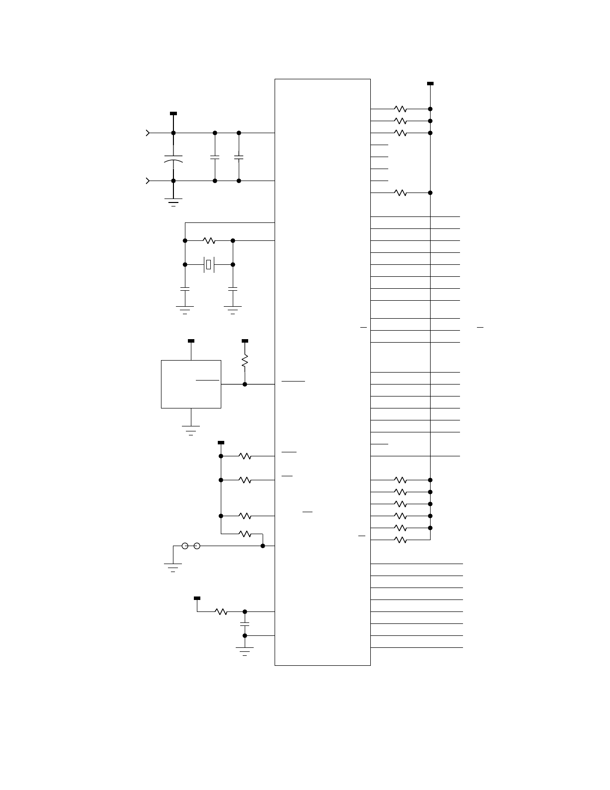
M68HC11 CONFIGURATION AND MODES OF OPERATION MOTOROLA
REFERENCE MANUAL 3-21
Figure 3-1 Schematic for Figure 3-3 (Sheet 1 of 2)
VDD
+
4.7K
MC34064
VDD
RESET
VDD
GND
IN
1K
1µF
VDD
10M
8.0 MHz
18 pF
18 pF
VDD
4.7K
4.7K
0.01 µF
10 µF
SYSTEM
POWER
CUT
JUMPER FOR
NORMAL MODE
RESET
XIRQ
IRQ
V
V
RH
RL
MODA/LIR
V
STBY
MODB/V
DD
VSS
EXTAL
XTAL
MC68HC11A8
PA0/IC3
PA1/IC2
PA2/IC0
PA3/OC5/OC1
PA4/OC4/OC1
PA5/OC3/OC1
PA6/OC2/OC1
PA7/PAI/OC1
A8
A9
A10
A11
A12
A13
A14
A15
PE4/AN4
PE5/AN5
PE6/AN6
PD0/RxD
PD1/TxD
PD2/MISO
PD3/MOSI
PD4/SCK
PD5/SS
PE7/AN7
PE0/AN0
PE1/AN1
PE2/AN2
PE3/AN3
VDD
10K TYP
E
4.7K
4.7K
1µF
AS
AD0
AD1
AD2
AD3
AD4
AD5
AD6
AD7
R/W
10K TYP
A8
A9
A10
A11
A12
A13
A15
PE4
PE5
PE6
PE7
PE0
PE1
PE2
PE3
E
AS
AD0
AD1
AD2
AD3
AD4
AD5
AD6
AD7
R/W
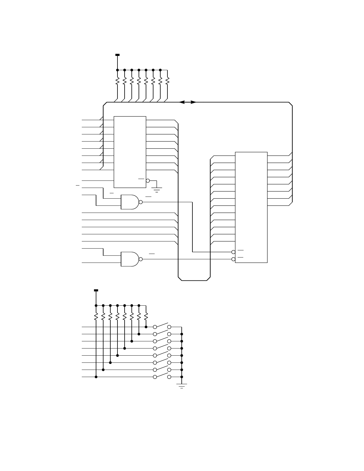
MOTOROLA CONFIGURATION AND MODES OF OPERATION M68HC11
3-22 REFERENCE MANUAL
Figure 3-2 Schematic for Figure 3-3 (Sheet 2 of 2)
DATA BUS
ADDRESS BUS
D0
D1
D2
D3
D4
D5
D6
D7
A0
A1
A2
A3
A4
A5
A6
A7
D0
D1
D2
D3
D4
D5
D6
D7
A8
A9
A10
A11
A12
8K X 8 EPROM
A0
A1
A2
A3
A4
A5
A6
A7
A8
A9
A10
A11
A12
OE
Q0
Q1
Q2
Q3
Q4
Q5
Q6
Q7
LE
D0
D1
D2
D3
D4
D5
D6
D7
74HC373 A0
A1
A2
A3
A4
A5
A6
A7
A8
A9
A10
A11
A12
D0
D1
D2
D3
D4
D5
D6
D7
E
R/W
DIP
SWITCH
CS
OE
D0 D1 D2 D3 D4 D5 D6 D7
10K TYP
10K TYP
HC00
HC00
A13
A15 CS
OE
VDD
VDD
A8
A9
A10
A11
A12
A13
A15
PE4
PE5
PE6
PE7
PE0
PE1
PE2
PE3
E
AS
AD0
AD1
AD2
AD3
AD4
AD5
AD6
AD7
R/W

M68HC11 CONFIGURATION AND MODES OF OPERATION MOTOROLA
REFERENCE MANUAL 3-23
***********************************************************************
*************************************************************************
*****
* Example 3–1 65 bytes total *
* *
* This example program uses the hardware setup in figure 3–1 in test *
* mode. After reset the CONFIG register is checked against port E. *
* If it is different, CONFIG is erased and reprogrammed to the port E *
* value. $30 is written to port A and the program ends. *
*************************************************************************
*****
ORG $A000 Start of external EPROM
EX31A LDS #$00FF Establish top of stack
BSR DLY10 Allow charge pump to stabilize
LDAA $100A Read port E DIP switches
ANDA #$0F Mask off upper 4 bits (not implemented on ’A8)
CMPA $103F See if CONFIG is same
BEQ NOWOK If already OK
* Not OK so first erase CONFIG
LDAB #$06 Bulk Erase, and EELAT on
STAB $103B Write to PPROG register
STAA $103F Write to CONFIG address (any data)
INCB To $07 - turns on EEPGM bit
STAB $103B Write to PPROG register
BSR DLY10 Delay 10 ms for erase to complete
CLR $103B Turn off charge pump (EEPGM to 0)
* Now reprogram CONFIG with data from port E (still in A-reg)
LDAB #$02 Turn on EELAT
STAB $103B Write to PPROG register
STAA $103F Write port E data to CONFIG address
INCB To $03 - Turns on EEPGM bit
STAB $103B Write to PPROG register
BSR DLY10 Delay 10 ms for erase to complete
CLR $103B Turn off charge pump (EEPGM to 0)
* Programming complete but you can’t check results till next reset
NOWOK LDA #$30
STAA $1000 You are done (check with scope)
BRA * Branch to self (hangs till pwr off or rst)
*
* PR0GRAM END subroutines follow
*
***
* DLY10 - Subroutine to delay l0ms (for E=2MHz)
***
DLY10 PSHX Save X (not required in this ex I just do)
LDX #$0D06 3334 6~ * 500nS/~ = l0mS
DLOOP DEX [3] in []s is cycles for that instruc
BNE DLOOP [3] cont. for 3334 times (loop time = 6~)
PULX Recover X value
RTS **RETURN**
*
* Establish a reset vector
*
ORG $BFFE
RESET FDB $A000 Point to start of program
Figure 3-3 Program to Check/Change CONFIG

MOTOROLA CONFIGURATION AND MODES OF OPERATION M68HC11
3-24 REFERENCE MANUAL

M68HC11 ON-CHIP MEMORY MOTOROLA
REFERENCE MANUAL 4-1
SECTION 4
ON-CHIP MEMORY
The MC68HC11A8 includes on-chip random-access memory (RAM), read-only mem-
ory (ROM), and electrically erasable programmable ROM (EEPROM) memories. The
on-chip RAM is a fully static read-write memory used for storage of variable and tem-
porary information. The MC68HC11A8 has 256 bytes of RAM; whereas other mem-
bers of the M68HC11 Family include more or less RAM (MC68HC11E9 has 512 bytes
of RAM and MC68HC11D3 has 192 bytes of RAM). Members of the M68HC11 Family
include various amounts of on-chip mask-programmed ROM. The MC68HC11A8 has
8 Kbytes of user ROM, the MC68HC11E9 has 12 Kbytes, and the MC68HC11D3 has
4 Kbytes. This ROM is used for storage of user program instructions and fixed data.
Some members of the M68HC11 Family have this internal ROM disabled, and the user
programs reside in external memories. The last major memory system on the
M68HC11 is the EEPROM. The MC68HC11A8 includes 512 bytes of EEPROM;
whereas other members of the M68HC11 Family include as much as 8.5 Kbytes of EE-
PROM. Data can be programmed into the EEPROM or erased from the EEPROM un-
der software control. No power supplies other than the normal VDD (5 Vdc) supply are
needed for programming or erasure of the 512 bytes of on-chip EEPROM in the
MC68HC11A8. No power supplies are required to maintain the contents of this mem-
ory. This memory is commonly used for semipermanent information such as calibra-
tion tables, personality data, or product history information. The EEPROM can also be
used for program memory; furthermore, the non-volatile nature of this EEPROM sup-
ports programs that can adapt to changing conditions.
4.1 ROM
The primary use for on-chip ROM is to hold the user’s application program instructions.
Since these instructions are programmed into the microcontroller unit (MCU) when it
is manufactured, they cannot be changed. A user develops the application program
and debugs it before ordering production MCUs. The user places an order for produc-
tion units with the pattern of instructions and data to be programmed into the on-chip
ROM. Motorola then translates this pattern into a photographic mask to be used during
processing of silicon wafers. Motorola then produces a small batch of these parts and
returns them to the customer for verification. These units are called ROM verification
units (RVUs). After customer approval of these RVUs, Motorola begins full production
of these customized MCUs. The RVUs, processed on a quick turnaround basis, are
not tested to environmental extremes because their sole purpose is to demonstrate
that the customer-requested ROM pattern was properly implemented.
The on-chip program ROM can be disabled by an EEPROM-based control bit in the
configuration control (CONFIG) register. When the program ROM is disabled, it uses
up no space in the 64-Kbyte memory space, and an external memory is used for pro-
gram instructions. ROM-less versions of the M68HC11 Family, such as the
MC68HC11A1, actually have on-chip ROM, but the ROM is disabled by the enable on-

MOTOROLA ON-CHIP MEMORY M68HC11
4-2 REFERENCE MANUAL
chip ROM (ROMON) control bit equals zero in the CONFIG register.
The MC68HC11A8 actually has two separate on-chip ROM memories — the 8-Kbyte
user ROM, which is available for user-defined programs, and a separate 192-byte
ROM, called the bootloader ROM. This bootloader ROM controls the bootstrap loading
process of the special bootstrap mode. In normal modes of operation, the bootloader
ROM is disabled and uses no space in the 64-Kbyte address space of the MCU. Dur-
ing expanded test mode, the bootloader ROM can be enabled for testing but is not in
the memory map after a reset until/unless the test program software enables it. In spe-
cial bootstrap mode, the bootloader ROM is enabled at $BF40–$BFFF by default out
of reset, and the reset Vector in this ROM at $BFFE,BFFF Vectors to the bootloader
program in this ROM.
The bootloader program is also involved with the security feature that allows a user to
protect the contents of EEPROM and RAM from being read by software pirates. When
the security option is enabled, the MCU can only be reset in normal single-chip mode
or special bootstrap mode. In normal single-chip mode, the reset vector is located in
the on-chip 8-Kbyte ROM, and the user’s program controls all program actions. Since
there are no external address or data buses, a pirate could not see what is in the in-
ternal EEPROM or RAM memories. In special bootstrap mode, the reset vector is lo-
cated in the on-chip bootloader ROM, and the bootloader program is in control. The
bootloader program checks the security enable control bit before proceeding to the
program downloading step. If security is enabled, the entire EEPROM and RAM are
erased before downloading continues. After the EEPROM and RAM have been
erased and verified, the CONFIG register (which contains the security enable control
bit) is erased, and downloading can proceed. For additional information about the
CONFIG register and security option, refer to 3.2 EEPROM-Based CONFIG Regis-
ter.SECTION 3 CONFIGURATION AND MODES OF OPERATION also includes ad-
ditional details about modes of operation.
4.2 RAM
This subsection discusses the on-chip RAM of the MC68HC11A8. This 256-byte RAM
can be mapped to the beginning of any 4-Kbyte block in the 64-Kbyte address space.
The methods and reasons for this remapping are discussed; two methods of RAM
standby are also discussed.
4.2.1 Remapping Using the INIT Register
By default, the on-chip RAM is located in the first 256 locations ($0000–$00FF) of the
64-Kbyte memory map. In many (but not all) cases, this location is good for the on-chip
RAM. The first 256 locations in memory are accessible using the direct addressing
mode, which assumes the upper byte of the 16-bit address is $00. Since the direct ad-
dressing mode can address these locations with a one-byte address rather than a two-
byte address, each such instruction saves a byte of program memory space and a cy-
cle of execution time compared to the same instruction using expanded addressing
mode. Depending upon the application, maximum efficiency can be achieved by hav-
ing RAM, I/O registers, or both in this premium address space.

M68HC11 ON-CHIP MEMORY MOTOROLA
REFERENCE MANUAL 4-3
The position of RAM in the 64-Kbyte address space is controlled by the RAM and I/O
mapping (INIT) register. The upper four bits of INIT (RAM[3:0]) specify the upper four
bits of the 16-bit RAM addresses. At reset, the RAM[3:0] bits are forced to zero so the
RAM is initially located at $0000–$00FF. By writing some other value to the INIT reg-
ister, the RAM can be relocated to the beginning of any 4-Kbyte page in the 64-Kbyte
address space. In normal operating modes, the INIT resister is protected so that it can
only be changed within the first 64 cycles after reset. For more detailed information
about the INIT register, see 3.3.1 RAM and I/O Mapping Register (INIT).
4.2.2 RAM Standby
There are several purposes for a RAM standby function. In battery operated systems,
the RAM standby function provides a way to conserve limited battery power during
times of MCU inactivity, which increases the effective time the system can operate
without battery charging or replacement. In systems using a municipal electric system
as the primary source of power, operating power is not usually a major issue, but pow-
er interruptions can be. There may be enough energy stored in regulator filter capac-
itors to allow a system to operate for some period of time after primary power is lost.
The system current drain determines how long the stored energy can maintain the sys-
tem. By detecting the loss of primary power and changing to a low-power standby
mode, the MCU system can be maintained through longer power interruptions. After
the interruption, the system can decide whether to continue operation or to perform a
complete reset initialization. In other municipal-powered systems, it may be useful to
maintain a limited amount of information during very long interruptions of primary pow-
er. In such cases, a separate standby power source based on a battery could be used
to maintain the contents of RAM while the system is non-operational.
The on-chip RAM of the M68HC11 Family is fully static; there are two ways RAM con-
tents can be maintained while reducing system power consumption to very low levels.
The easiest method for low-power RAM standby is the software-based STOP mode.
The alternate method uses the MODB/VSTBY pin for standby power in a mostly hard-
ware approach. Since the entire MCU, including RAM, is fully static, there is no mini-
mum oscillator clock frequency. In complementary metal oxide semiconductor
(CMOS) integrated circuits, power supply current is directly proportional to operating
frequency; thus, only very small leakage currents exist when clocks are stopped. This
is the basis for the STOP method of RAM standby. When the MCU is stopped, all CPU
registers, control and I/O registers, and all RAM contents remain unchanged as long
as VDD is present. IDD for the MCU is reduced to a few microamps when MCU clocks
are stopped.
In some systems, there may be other circuitry powered from VDD that cannot be easily
placed in a low-power standby mode. In these systems, VDD must be turned off to re-
duce system power drain. The MODB/VSTBY method of RAM standby allows VDD to
be removed without losing the contents of on-chip RAM. This method is more hard-
ware intensive because it involves a second power supply and associated problems.
In CMOS systems, it is possible to power an integrated circuit through an I/O pin be-
cause, on some I/O pins, there is an inherent diode between the pin and the internal
VDD. In some CMOS systems, even the sequencing of power supplies is critical, which

MOTOROLA ON-CHIP MEMORY M68HC11
4-4 REFERENCE MANUAL
implies using caution whenever there is more than one power supply in a system. Al-
though the sequencing of VDD relative to MODB/VSTBY is not important on the
MC68HC11A8 itself, the sequencing may be important to any other CMOS device in
the system exposed to both VDD and VSTBY.
Several I/O pins on the MCU should not have voltage on them while VDD is off. Any
pin having the source or drain node of a P-channel device in the on-chip circuitry con-
nected to this pin has an inherent diode to VDD. If such a pin were connected to a sig-
nal powered by VSTBY rather than VDD, the entire VDD network would be powered by
VSTBY through the inherent diode. Powering the VDD network in this way may result in
unexpected operation of the system and definitely results in more load on the VSTBY
supply than expected.
4.3 EEPROM
The MC68HC11A8 was the first MCU to include CMOS EEPROM. This 512-byte EE-
PROM memory can be used in the same ways ROM would be used, but some inter-
esting possibilities arise that are not possible with ROM or RAM memories. A simple
example is to store a unique serial number in the EEPROM of each finished product.
Once information is programmed into the on-chip EEPROM, it remains unchanged
even if VDD power is removed indefinitely. Unlike information in ROM, information in
EEPROM can be erased or reprogrammed under software control. Since EEPROM
programming and erasure operations use an on-chip charge pump driven by VDD,no
special power supplies are needed.
This subsection describes the operation of the EEPROM on the MC68HC11A8 and
explores some of its applications. In addition to the 512 bytes of user EEPROM on the
MC68HC11A8, there is another EEPROM byte (CONFIG register) controlling some
basic features of the MCU. The CONFIG register and mechanism are described in de-
tail in 3.2 EEPROM-Based CONFIG Register, but some aspects of the EEPROM en-
able bit (EEON), and the security mode disable bit (NOSEC) will be discussed in terms
of how they relate to EEPROM.
The M68HC11 Family of MCUs includes members with various amounts of EEPROM.
The MC68HC811A8 (emulator for the basic MC68HC11A8) has 8.5 Kbytes of EE-
PROM. The principles presented here apply specifically to the original MC68HC11A8.
Some details of EEPROM operation may vary slightly for other members of the
M68HC11 Family; however, the basic concepts presented here can be extended to
explain the operation of these other members.
4.3.1 Logical and Physical Organization
The logical organization of the 512-byte EEPROM is important for identification of
rows when using the row-erase feature. The physical organization may be useful in
isolating problems in rare cases.
Although some Family members (e.g., MC68HC811E2) allow remapping of the on-
chip EEPROM, the 512-byte EEPROM in the MC68HC11A8 is fixed at locations
$B600–$B7FF. This 512-byte block is logically arranged into 32 rows of 16 bytes each.
The first row occupies the locations $B600–$B60F, the second row occupies $B610–
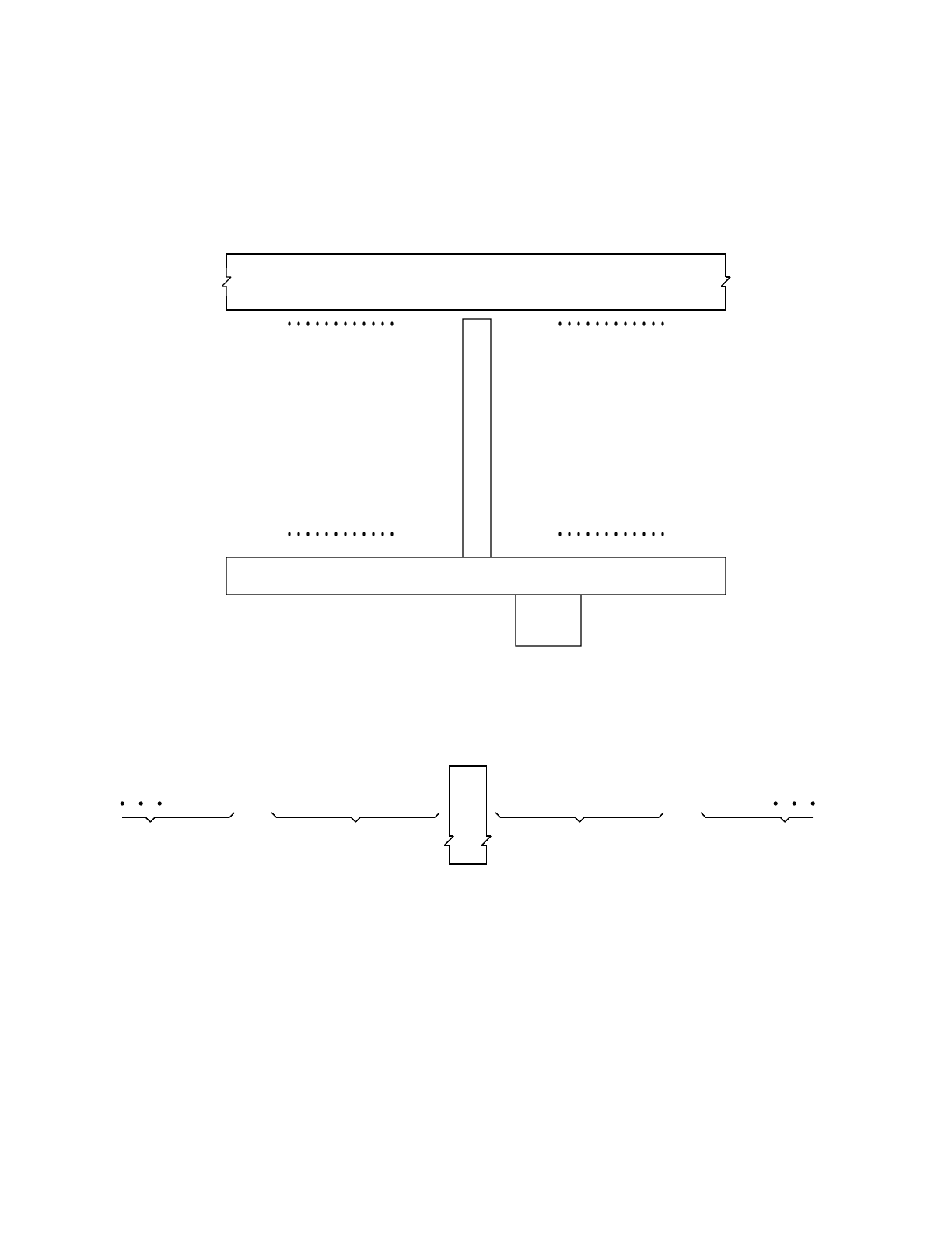
M68HC11 ON-CHIP MEMORY MOTOROLA
REFERENCE MANUAL 4-5
$B61F, etc. EEPROM locations can be erased individually (byte erase), in rows of 16
bytes each (row erase), or all 512 bytes at once (bulk erase). The CONFIG byte is sep-
arate from this 512-byte block. Special restrictions apply to erasure of the CONFIG
EEPROM byte. Figure 4-1 shows the topological organization of the 512 bytes of EE-
PROM in the MC68HC11A8. Figure 4-2 shows the topological arrangement of bits
within a byte of EEPROM.
Figure 4-1 Topological Arrangement of EEPROM Bytes (MC68HC11A8)
Figure 4-2 Topological Arrangement of Bits in an EEPROM Byte
4.3.2 Basic Operation of the EEPROM
The following paragraphs briefly describe how the EEPROM operates. Figure 4-3,a
condensed schematic of the EEPROM array, provides insight into the operation of the
EEPROM system and illustrates the complexity of a byte-erasable EEPROM. Each
byte in the EEPROM array consists of 17 transistors, eight floating-gate transistors, a
select transistor for each floating-gate transistor, and a byte-select transistor. In com-
parison, an ultraviolet erasable EPROM byte requires only the eight floating-gate tran-
B7E1 B7E0
ARRAY
LEFT HALF
B62F B620
B64F B640
B66F B660
B68F B680
B6AF B6A0
B6CF B6C0
B6EF B6E0
B70F B700
B72F B720
B74F B740
B76F B760
B78F B780
B7AF B7A0
B7CF B7C0
B60F B60E B601 B600
B7EF B7EE B7FE B7FF
ARRAY
RIGHT HALF
B630 B63F
B650 B65F
B670 B67F
B690 B69F
B6B0 B6BF
B6D0 B6DF
B6F0 B6FF
B710 B71F
B730 B73F
B750 B75F
B770 B77F
B790 B79F
B7B0 B7BF
B7D0 B7DF
B610 B611 B61E B61F
B7F0 B7F1 CONFIG ROW
COLUMN DECODERS AND SENSE AMPS
ROW DECODERS AND DRIVERS
CHARGE
PUMP
ROM ARRAY
FOR LEFT HALF FOR RIGHT HALF
B601 B600 B610 B611
BIT 7 BIT 7 BIT 7BIT 7 BIT 0 BIT 0654321 65432165 65
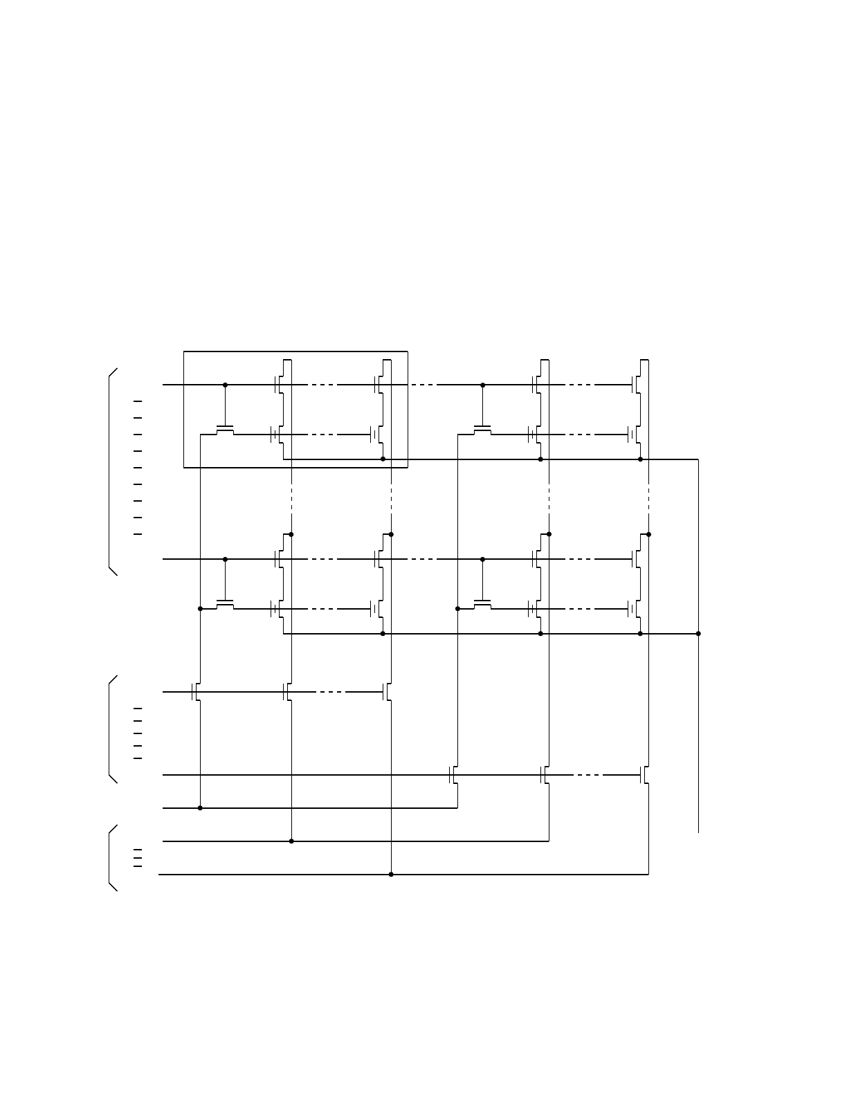
MOTOROLA ON-CHIP MEMORY M68HC11
4-6 REFERENCE MANUAL
sistors.
Figure 4-4 shows an EEPROM bit with important features and nodes labeled. These
terms will be used in the following explanation of basic EEPROM operations. Figure
4-5,Figure 4-6, and Figure 4-7 show an EEPROM byte being erased, programmed,
and read, respectively. The floating-gate transistor is the storage element in the EE-
PROM cell. Since the floating gate is isolated by thin oxide layers, any charge on this
gate remains indefinitely unless a large enough field is created, as in programming
and erase modes. When a large enough field is present, Fowler-Nordheim electron
tunneling allows charge to be transferred to or from the floating gate, depending on the
polarity of the field. In the following discussion, VDD is nominally 5 V and VPP is about
20 V. In the MC68HC11A8, VPP is developed from VDD with an on-chip charge pump;
thus, no external high voltages are required.
Figure 4-3 Condensed Schematic of EEPROM Array
1 BYTE
ROW (0)
ROW (N)
COL (0)
COL (N)
V
I/O (7)
I/O (0)
ERASE
ARRAY
GROUND
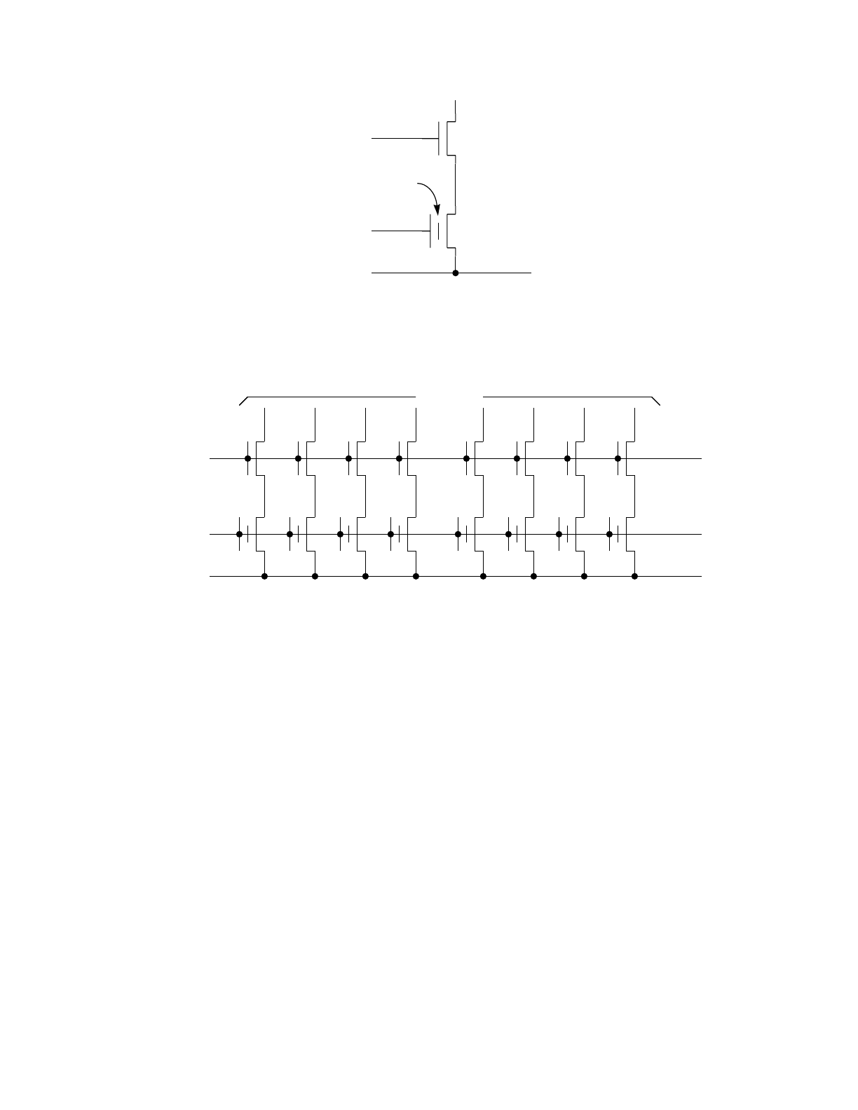
M68HC11 ON-CHIP MEMORY MOTOROLA
REFERENCE MANUAL 4-7
Figure 4-4 EEPROM Cell Terminology
Figure 4-5 Erasing an EEPROM Byte
In erase mode (see Figure 4-5), the array ground is connected to VSS. The row and
column selects cause the control gates of the byte(s) being erased to be connected to
VPP. Other bytes in the array that are not being erased would have their control gates
connected to an undriven logic zero. The bit-select devices are all turned on by VPP
on the word lines; however, the drains of the bit-select devices are high impedance.
Thus, the drains of the floating-gate transistors are effectively floating. The high volt-
age on the control gate of the floating-gate transistor is capacitively coupled onto the
floating gate. The large field between the floating gate and the substrate results in
electron tunneling from the substrate to the floating gate. After erasure, the floating
gate has a negative charge, which keeps the floating-gate transistor turned off during
reads. If leakage in the floating-gate transistor caused the negative charge to leak off
so that there was no charge on the floating gate, the bit would still read back as one.
This fact implies that long-term retention errors cannot cause a logic-one bit to deteri-
orate to a logic zero.
Figure 4-6 shows an EEPROM byte being programmed to the value $55 (0101 0101)
ARRAY GROUND
BIT LINE
BIT-SELECT
DEVICE
FLOATING-GATE
DEVICE
ROW
SELECT
CONTROL
GATE
FLOATING GATE
S
D
G
ARRAY GROUND
7
VPP
NOT DRIVEN
654 3210
VTN
VSS
VPP —
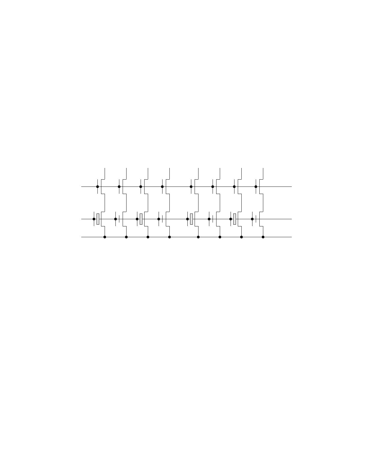
MOTOROLA ON-CHIP MEMORY M68HC11
4-8 REFERENCE MANUAL
to demonstrate the effect of programming both ones and zeros. Since the erased state
of an EEPROM bit is one, programming a one is the same as doing nothing. During
programming, the array ground is not driven. The control gates of the byte to be pro-
grammed are driven to zero through the row-select and column-select path. Control
gates for bytes not being programmed will be high impedance because the column-
select and/or row-select device will be off. The bit-select devices are turned on hard
because the row select, for the row containing the byte being programmed, is driven
to VPP. The bit lines are driven to VDD for bits not being programmed (ones) and to
VPP for bits being programmed (zeros).
For bits not being programmed (ones), the drain of the floating-gate transistor is at
VDD, and the control gate is at VSS. This configuration does not result in a large
enough field for tunneling to occur; thus, no charge transfer occurs.
Figure 4-6 Programming an EEPROM Byte
For bits being programmed (zeros), the drains of the floating-gate transistors are at
VPP –V
TN (because of the drain-to-source threshold voltage drop across the bit-select
device), and the control gate is at VSS. This configuration results in a large enough field
so electrons can tunnel from the floating gate to the drain region of the floating-gate
transistor. Since the floating gate of a programmed bit has a positive charge, the float-
ing-gate transistor will conduct during reads.
Figure 4-7 shows an EEPROM byte being read. During a read operation, the bit lines
are precharged to one. Column selects enable the bit lines from the byte being read
to the sense amp inputs. The row select for the row containing the byte being read is
driven to VDD to enable the bit-select devices. The array ground is connected to VSS.
The floating gate devices of programmed bits conduct and pull the corresponding bit
lines to zero. The floating-gate devices of bits not programmed do not conduct; there-
fore, the corresponding bit lines remain at the precharged level and read as ones. EE-
PROM operations are actually much more complicated than this discussion suggests,
but the following general statements may be useful to designers using the EEPROM.
1) Since no high voltages are present during read operations, no degradation of data
ARRAY GROUND
7
VPP
654 3210
VSS
(NOT DRIVEN)
0101 0101
VPP VDD VPP VDD VPP VDD VPP VDD
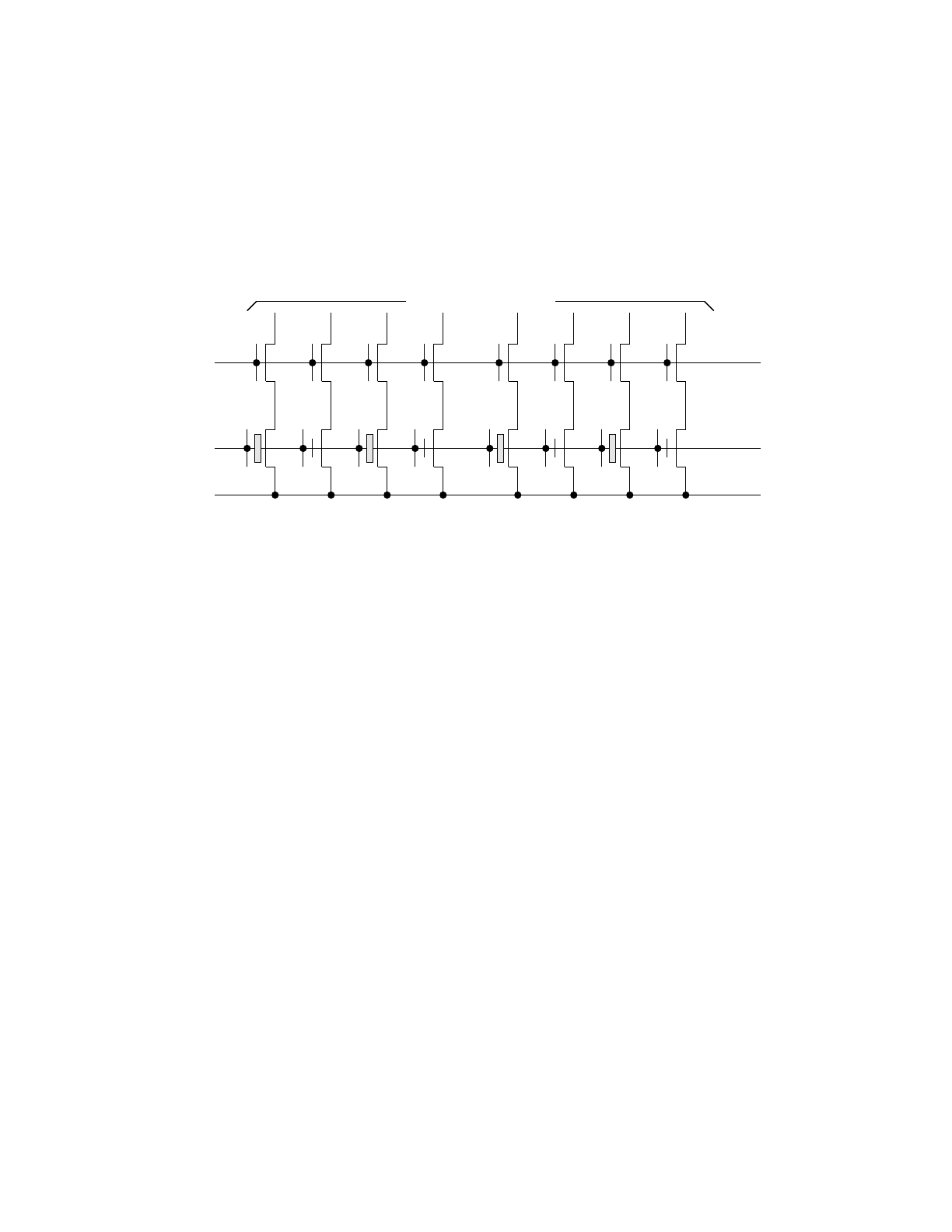
M68HC11 ON-CHIP MEMORY MOTOROLA
REFERENCE MANUAL 4-9
can result from repeated read operations. 2) Erase operations normally take less time
than programming operations. 3) The most common EEPROM failure (write ones) is
an unintended bit change from one to zero during programming of $FF data. This fail-
ure occurs during endurance testing as the part approaches wear-out (typically after
tens of thousands of write-erase cycles). 4) Retention failures result in programmed
zeros reverting to ones due to leakage of the floating-gate charge. 5) Ones never re-
vert to zeros without an explicit programming operation (though the programming op-
eration need not involve any zeros in the pattern being programmed).
Figure 4-7 Reading an EEPROM Byte
EEPROM programming and erasure involve the movement of charge through a thin
oxide layer. This charge movement requires a relatively large field to be present for a
significant length of time (milliseconds). Noise is not likely to cause individual bits to
change state. Most failures of the EEPROM involve breakdowns due to the relatively
high voltages or to an oxide degradation phenomenon (trapped charge). After many
cycles of programming and erasure, charge may become trapped in the thin oxide lay-
ers isolating the floating gate. This trapped charge causes programming and erase op-
erations to take longer as the amount of trapped charge increases. When the cell fails
to program to zero in the allotted time, it is worn out. In many cases, these bits can still
be programmed and erased provided the program and erase times are increased. The
useful life of an EEPROM byte cannot be extended very far by extending the program-
ming time because a worn bit exhibits a reduced ability to retain valid zeros for very
long time periods.
4.3.3 Systems Operating below 2-MHz Bus Speed (E Clock)
The on-chip charge pump that generates VPP from VDD uses MOS capacitors, which
are relatively small in value. The efficiency of this charge pump and its drive capability
are affected by the level of VDD and the frequency of the driving clock. The load de-
pends on the number of bits being programmed or erased and capacitances in the EE-
PROM array. Effective array load capacitances are influenced to some degree by the
data in the array.
The clock source driving the charge pump is software selectable. When the clock se-
ARRAY GROUND
7
VDD
654 3210
VSS
VSS
PRECHARGE THEN SENSE

MOTOROLA ON-CHIP MEMORY M68HC11
4-10 REFERENCE MANUAL
lect (CSEL) control bit in the OPTION register is zero, the E clock is used; when CSEL
is one, an on-chip resistor-capacitor (RC) oscillator is used. The frequency of this on-
chip RC oscillator is about 2.5 MHz but varies with processing.
The recommended programming and erase time is 10 ms when VDD is 5 Vdc ±10 per-
cent and the E clock is 2 MHz. If the E clock is 1 MHz or less, the CSEL bit should be
written to one to enable the on-chip RC oscillator to drive the VPP charge pump. For
an E clock between 1 and 2 MHz, the programming and erase times can be increased
to 20 ms, or the RC oscillator can be selected. Experimentation has shown the EE-
PROM is programmable with VDD equal to 3 Vdc and CSEL equals one to enable the
on-chip RC clock.
CSEL also enables a separate RC oscillator associated with the A/D converter sys-
tem. The E-clock frequency (where switchover to CSEL equals one is recommended)
is lower for the A/D than it is for EEPROM operations. In the A/D system, switching to
CSEL equals one can increase conversion errors; thus, it is better to perform A/D con-
versions with CSEL equals zero. In some applications, it is worthwhile to switch CSEL
on and off, depending on whether A/D or EEPROM programming/erase operations are
occurring. Refer to 12.2.2 A/D Charge Pump and Resistor-Capacitor (RC) Oscilla-
tor for additional information.
4.3.4 EEPROM Programming Register (PPROG)
The PPROG register controls programming and erasure of the on-chip EEPROM. The
PPROG register may be read or written at any time, but programming and erase se-
quences are strictly controlled by logic to prevent unintentional changes to EEPROM
data. In the MC68HC11A8, the CONFIG register EEPROM location cannot be pro-
grammed or erased unless the MCU is operating in special test or special bootstrap
mode. The VPP power supply voltage is not enabled to the EEPROM array until all se-
quence requirements are met for a programming or erase operation. The required se-
quence consists of the following steps: 1) write to PPROG with EEPROM latch control
(EELAT) bit equals one and EEPROM programming voltage enable (EEPGM) bit
equals zero; 2) write to a valid EEPROM location or the CONFIG address; 3) write to
PPROG with EELAT and EEPGM bits equal one. Hardware logic enforces this se-
quence by imposing the following restrictions. If an attempt is made to change both
EELAT and EEPGM to ones with the same write operation, neither bit is set (enforces
step 1). Writes to EEPROM addresses are inhibited while EEPGM is one, which pre-
vents two kinds of errors. First, step 2 must be performed before step 3, or no EE-
PROM changes will occur. Second, a write to a different EEPROM location is
prevented while a programming or erase operation is in progress.
In some members of the M68HC11 Family, there is a block protection mechanism that
can inhibit programming and erasure of the CONFIG register or selected areas of EE-
PROM. After reset, these block protect control bits (in a block protect (BPROT) regis-
ter) are set to inhibit EEPROM changes. A user can write these bits to zero to enable
programming and erase operations, but this write must be performed within 64 cycles
after reset. The user may write these bits back to one at any time to inhibit further EE-
PROM changes. Once this protection is re-enabled, it remains in effect until another
reset. There is no BPROT register in the MC68HC11A8.
M68HC11 ON-CHIP MEMORY MOTOROLA
REFERENCE MANUAL 4-11
The following register and paragraphs describe the bits in the PPROG control register.
ODD — Program odd rows in half the EEPROM array
EVEN — Program even rows in half the EEPROM array
These two bits are used only during factory testing of the EEPROM. To program all
bytes in the odd (even) rows on one side of the EEPROM array with the same data in
a single programming operation, set the ODD (EVEN) and EELAT bits to ones, write
to an EEPROM location in an odd (even) row, and then set the EEPGM bit. Since the
onchip VPP charge pump does not have enough drive to perform this bulk program-
ming operation, an external 20-V current-limited supply must be connected to the ex-
ternal EEPROM voltage source (IRQ/VPPBULK) pin. The intended purpose of this
function is to allow the entire EEPROM array to be filled with a checkerboard pattern
in only four programming operations. This feature is not intended for customer use
since the function serves no practical purpose other than product testing.
BYTE — Byte/Other EEPROM Erase Mode
ROW — Row/All EEPROM Erase Mode
These two bits specify the type of erase operation that is to be performed. These bits
have no meaning when the ERASE bit is clear. The following table shows the relation-
ship between the state of these bits and the type of erase operation that will be per-
formed:
ERASE — Erase/Normal Control of EEPROM
0 = Normal read or program mode
1 = Erase mode
EELAT — EEPROM Latch Control
When this bit is zero, the EEPROM acts as a ROM in the MCU memory map. When
EELAT is one, the EEPROM acts as if it has been removed from the memory map and
placed into a programming socket. Latches on the address and data lines to the
EEPROM array are enabled to capture data and address information needed during
program or erase operations. While EELAT is one, the EEPROM cannot be read,
which implies a software routine that programs or erases EEPROM cannot be execut-
ed from that same EEPROM. The operation of EELAT also implies that programs that
access data from the EEPROM must not be executed while an EEPROM location is
being programmed or erased.
PPROG — EEPROM Programming Register $103B
BIT 7 654321BIT 0
ODD EVEN 0 BYTE ROW ERASE EELAT EEPGM
RESET: 00000000
BYTE ROW Type of Erase
0 0 Bulk Erase (All 512 Bytes)
0 1 Row Erase (16-Byte Row)
1 0 Byte Erase
1 1 Byte Erase

MOTOROLA ON-CHIP MEMORY M68HC11
4-12 REFERENCE MANUAL
EEPGM — EEPROM Programming Voltage Enable
This control bit enables the VPP power supply to the EEPROM logic for programming
and erase operations. When EEPGM is zero, VPP is off; when EEPGM is one, VPP is
on. A logic interlock mechanism prevents setting this bit unless EELAT was earlier
written to one.
4.3.5 Programming/Erasing Procedures
The following discussion and program segments demonstrate the various program-
ming and erase operations that can be performed on EEPROM locations. These pro-
gram segments are intended to be simple, straightforward examples of the sequences
needed for basic program and erase operations. There are no special restrictions on
the addressing modes used, and bit manipulation instructions may be used. Other op-
erations can be performed during programming and erasure provided these opera-
tions do not include reads from the EEPROM (the EEPROM is disconnected from the
read data bus during program and erase operations). The subroutine (DLY10) used in
these program segments is not shown but can be any set of instructions that takes 10
ms.
If several bytes of EEPROM are to be programmed, the EELAT bit can be left at one
for the entire block. After each byte is programmed, EEPGM is written to zero and EE-
LAT is left at one. The next EEPROM location is then written, and the EEPGM bit is
written back to one to execute the programming request.
4.3.5.1 Programming
During EEPROM programming, the ROW and BYTE bits are not used. If the E-clock
frequency is less than 2 MHz, the programming time may need to be increased, or the
CSEL bit in the OPTION register may have to be set to enable an on-chip RC oscillator
to drive the VPP charge pump. Since programming can only change ones to zeros in
the EEPROM, it is sometimes necessary to erase a byte to $FF in a separate opera-
tion before programming it to a new value. The following programming segment dem-
onstrates how to program an EEPROM byte:
* On entry, A = data to be programmed and X = an EEPROM address
"
"
PROG LDAB #$02
STAB $103B Set EELAT bit (EEPGM=0)
STAA 0,X Store data to EEPROM address
LDAB #$03
STAB $103B Set EEPGM bit (EELAT=1)
JSR DLY10 Delay 10 mS
CLR $103B Turn off high voltage & set to read mode
"
"
4.3.5.2 Bulk Erase
The following program segment demonstrates how to bulk erase the 512-byte
EEPROM. The CONFIG register is not affected in this example.

M68HC11 ON-CHIP MEMORY MOTOROLA
REFERENCE MANUAL 4-13
"
"
BULKE LDAB #$06
STAB $103B Set to BULK erase mode
STAB $B600 Write any data to any EEPROM address
LDAB #$07
STAB $103B Turn on programming voltage
JSR DLY10 Delay 10 mS
CLR $103B Turn off high voltage & set to read mode
"
"
4.3.5.3 Row Erase
The following example demonstrates the row-erase function. A row is 16 bytes
($B600–B60F, $B610–B61F ... $B7F0–B7FF). When large sections of EEPROM are
to be erased, this type erase operation saves time compared to byte erase.
* On entry, X=any address in ROW to be erased
"
"
ROWE LDAB #$0E
STAB $103B Set to ROW erase mode
STAB 0,X Write any data to any address in ROW
LDAB #$0F
STAB $103B Turn on high voltage
JSR DLY10 Delay 10 mS
CLR $103B Turn off high voltage & set to read mode
"
"
4.3.5.4 Byte Erase
The following program segment demonstrates how to erase a single byte of EEPROM.
* On entry, X=any address of BYTE to be erased
"
"
BYTEE LDAB #$16
STAB $103B Set to BYTE erase mode
STAB 0,X Write any data to address to be erased
LDAB #$17
STAB $103B Turn on high voltage
JSR DLY10 Delay 10 mS
CLR $103B Turn off high voltage & set to read mode
"
"
4.3.5.5 CONFIG Register
The following program segment shows how to program the CONFIG register in the
MC68HC11A8 to a new value. The CONFIG byte can only be erased with the bulk-
erase method on the original MC68HC11A8; however, some new members of the
M68HC11 Family allow the CONFIG byte to be byte erased. If any question arises
about which members can use byte erase, refer to the technical summary for that
member. It is possible to program additional bits in CONFIG to zero without erasing

MOTOROLA ON-CHIP MEMORY M68HC11
4-14 REFERENCE MANUAL
the location first; however, it is better to perform an erase first as shown in this example
and explained in 4.4 EEPROM Application Information.
* On entry, A-data to be programmed into CONFIG
"
"
CNFCH LDAB #$06
STAB $103B Set to BULK erase mode
STAB $103F Write any data to CONFIG address
LDAB #$07
STAB $103B Turn on programming voltage
JSR DLY10 Delay 10 mS
LDAB #$02
STAB $103B Turn off EEPGM, leave EELAT on
STAA $103F Store new CONFIG data
LDAB #$03
STAB $103B Set EEPGM bit (EELAT-1)
JSR DLY10 Delay 10 mS
CLR $103B Turn off high voltage & set to read mode
"
"
4.3.6 Optional EEPROM Security Mode
There is an optional security mode feature that can be used to protect the EEPROM
and RAM contents from unauthorized access. Most MCU products are of little or no
use without the software programs that control them. By protecting the secrecy of the
program or a key part of the program, a product can be protected against unauthorized
duplication. The MC68HC11A8 solves the dilemma of protecting against unauthorized
access while permitting testing and recovery of protected parts for reuse.
The protection mechanism operates on the principle of restricting protected devices to
the single-chip modes of operation. Since single-chip modes do not allow visibility of
the internal address and data buses, the contents of memory locations cannot be mon-
itored externally. Since the user’s program has unlimited access to the internal EE-
PROM and RAM, it is still possible for the application program to read information out
of these memories, write new information into them, or even report the contents of
these memories via MCU I/O ports. The user can develop a program to enter secret
information into the MCU or to read secret information out of the MCU by some secret
access procedure. All or part of this secret access procedure should be programmed
in the EEPROM so that a software pirate could not decode the secret procedure by
disassembling the ROM program, which can be read after turning off the security
mode. Although the security mode can be turned off easily by anyone at any time, this
can only be done after the information in EEPROM and internal RAM have been com-
pletely erased.
Two conditions are required to engage the security option. First, the option must be
enabled by a mask option. This option is normally requested at the time the customer
submits the mask program for the internal 8-Kbyte ROM. Since this option is enabled
or disabled during physical manufacturing of the silicon die, the choice must be made
prior to manufacturing. Although this first level of enable makes the MCU capable of
being secured, it does not activate the security mode. The second requirement to en-

M68HC11 ON-CHIP MEMORY MOTOROLA
REFERENCE MANUAL 4-15
gage the security option is that the NOSEC bit in the CONFIG register be programmed
to zero. Programming NOSEC to zero does not engage the security mode unless the
MCU was manufactured with the capability to recognize the security option. The rea-
son for a two-level enable is to prevent accidental activation of the security option in
applications that never intend to use it.
Bootloader firmware is used to disengage the security option. Bootloader firmware
checks the NOSEC bit in CONFIG to determine whether or not the security option is
on. If security is on, the entire EEPROM is erased, and the entire RAM is written with
$FF to overwrite anything that was in RAM before. The EEPROM and RAM are then
rechecked to make sure the erase operations were successful. If the operations were
not successful, they are repeated until successful. Once the EEPROM and RAM have
been verified as erased, the CONFIG register is erased to disengage the security op-
tion, and the downloading operation is started. It is not necessary to actually download
a program via the bootstrap mode to disengage security. All that is required is to come
out of reset in the bootstrap mode. The security option is disengaged regardless of
whether anything is downloaded.
The presence of the security option can be detected while the MCU is in reset by forc-
ing the mode A (MODA) and mode B (MODB) pins to one and monitoring the strobe
A/address strobe (STRA/AS) pin. When MODA and MODB are ones, the normal ex-
panded mode is requested. If security is engaged, the STRA/AS pin will act as a high-
impedance input because the security option causes the MODA pin to be interpreted
as a zero even if it is a one. In single-chip modes, the STRA/AS pin is configured for
the strobe A input function. If the security mode is not engaged, the STRA/AS pin will
be acting as the address strobe output, which can easily be recognized on an oscillo-
scope. This checking procedure allows the security mode to be detected without dis-
engaging it. If the MODB pin were low in this experiment, the bootstrap mode would
be requested rather than the normal single-chip mode. In the case of MODB low, care
is required not to release reset because doing so would cause the security option to
be disengaged.
When developing a security strategy, the user should remember ROM contents are
not protected. A software pirate can disengage the security option, read the contents
of the internal ROM, and disassemble the programs and subroutines in that ROM.
Some measures to protect an application program intentionally make the program
more difficult to understand. Programs that are difficult to understand are also difficult
to develop and maintain. Careful documentation of the function and intent of every
written program is essential.
A key can be stored in EEPROM. A user can then be required to supply a matching
key value before the program will operate. This approach is somewhat weak because
all of the operational programs are intact in the ROM; thus, a software pirate could find
and bypass the key-checking routine. However, if the key-checking routine is repeated
in more than one way and place, this approach can make unauthorized access diffi-
cult.
Another approach would be to program a vital subroutine entirely within the EEPROM.
This approach is better than the previous key-checking approach because the ROM

MOTOROLA ON-CHIP MEMORY M68HC11
4-16 REFERENCE MANUAL
does not contain all of the programs needed to make the product function. The weak-
ness of this approach is that a software pirate can still duplicate the product after solv-
ing that one routine. The pirate also gains a development cost advantage over the
original manufacturer, because only part of the application program has to be devel-
oped.
Many application programs are modularly organized as a major loop consisting of calls
to submodules. The application relies on both the routines that are called and the order
in which they are called. A degree of security can be achieved by putting the major
loop (which calls all the subprograms) in the EEPROM. In this case, a software pirate
can decode the submodules, but the order of execution is not known. To make the pro-
gram more difficult to decipher, extra incorrect programs could be included in ROM.
The software pirate could not distinguish real routines from fake routines. There is a
useful side-effect of this approach. Since the major loop is resident in the EEPROM, it
can be changed to call a replacement or patch routine if one of the subprograms is
defective. Rather than throwing away the entire MCU, the EEPROM can be repro-
grammed to correct or replace the defective subprogram.
Another approach to software secrecy involves accessing variables indirectly through
a pointer stored in the EEPROM. The program in ROM could execute a sequence
such as loading X with the pointer value from EEPROM (LDX addr; LDAA 0,X). Since
the software pirate does not know what X points to, there is no way of knowing what
is being loaded into accumulator A. By mixing direct accesses and indirect accesses
to the same variables, the software pirate is unable to recognize that two accesses are
to the same variable.
4.4 EEPROM Application Information
Since EEPROM is a relatively new technology, very little published application infor-
mation exists. This subsection presents practices that could cause application prob-
lems and discusses several practical uses for EEPROM on an MCU. Next, there is a
discussion of the use of EEPROM in programs that adjust themselves to accommo-
date variable conditions. Many applications can benefit from this type of programming,
which is presently becoming practical because of the inclusion of EEPROM on an
MCU. The subsection concludes with a detailed look at some proposed methods to
extend the useful write-erase lifetime of the EEPROM.
4.4.1 Conditions and Practices to Avoid
When programming a new value over an old value in EEPROM without first erasing
the EEPROM location, it is very important to avoid certain data patterns. The most
common method for programming a new non-FF value to an EEPROM location con-
taining a non-FF value is to erase the location before programming the new value. This
procedure works for any combination of old and new data values. In less common sit-
uations in which an EEPROM location endures many write-erase cycles, it may be de-
sirable to program a new value over an old value without erasing the location first. This
procedure is only possible when the new value has no ones where the EEPROM lo-
cation already has a zero. A method called ‘write-more-zeros’ can be used to program
additional bits in an EEPROM location without erasing the location first, which elimi-

M68HC11 ON-CHIP MEMORY MOTOROLA
REFERENCE MANUAL 4-17
nates a write-erase cycle. Another method called ‘selective-write’ has been proposed
but has not been tested and characterized enough to be sure it will work in all cases.
In this method, the data pattern used in the programming operation would have ones
in all positions except the bits that are zeros in the new value but were ones in the pre-
vious value. The idea in this method is to avoid reprogramming bits already pro-
grammed. The benefits are theoretical and have not been proven. Although both of
these methods (write-more-zeros and selective-write) appear to work correctly in lab-
oratory experimentation, the combination of the two methods is known to fail. An ex-
ample of a failing combination would be to attempt to program $FC to a location that
previously contained the value $0D in an attempt to change the location to the value
$0C. In this case, bit 1 follows the write-more-zeros method; whereas, bits [4:7] follow
the selective-write method. A detailed explanation of this case is given in 4.4.7 Soft-
ware Methods to Extend Life Expectancy.
System software should be partitioned so that data and programs in EEPROM will
never be used while an EEPROM programming or erase operation is in progress.
When the EELAT control bit is set to one at the beginning of a program or erase oper-
ation, the EEPROM is electronically removed from the MCU memory map; thus, it is
not accessible during the programming or erase operation. Since it is possible to per-
form other tasks while the 10-ms EEPROM operation is in progress, it is fairly common
to start the operation and return to the main program until the 10 ms is completed. If a
routine in the main program or an interrupt tries to access a value in EEPROM while
a programming operation is in progress, that operation will fail since the EEPROM is
temporarily inaccessible.
In an interrupt-driven system, it may be possible for an asynchronous interrupt to occur
in the middle of an EEPROM programming or erase operation. Such an interrupt can
cause the programming or erase operation to extend beyond the normal 10-ms period.
A small extension of the programming or erase time will not damage the EEPROM or
compromise the intended operation. Repeated extension or long extensions may in-
volve a slight acceleration of write-erase wear-out because wear-out is related to the
length of time high voltages are present in the EEPROM array. The most significant
effects of wear-out occur near the beginning of a program or erase operation because
the charge tunneling activity follows an exponential decay curve, which implies that ex-
tensions of programming time should have very little effect on the EEPROM cell. An-
other risk, which is difficult to quantify, is the possibility of high-voltage breakdown of
row and column devices due to the presence of programming voltage. If programming
and erase times are extended, these devices are exposed to high voltages for a longer
time; thus, there is increased risk that a breakdown might occur.
In some systems, an EEPROM programming or erase operation could be in progress
when a power failure or reset occurs, which presents the possibility that an EEPROM
location might be corrupt or unreliable due to an incomplete programming operation.
A way to avoid this problem is to design the system so power failures generate a non-
maskable interrupt prior to complete loss of power. This interrupt would allow EE-
PROM operations to be completed prior to system shutdown. Other systems may
have battery backup of RAM so programming status could be maintained in this mem-
ory. Upon reset, this status (in RAM) could be checked, and any operation that was in

MOTOROLA ON-CHIP MEMORY M68HC11
4-18 REFERENCE MANUAL
progress could be redone to assure reliability.
Avoid unnecessary erasures of the CONFIG register EEPROM location. In a normal
system, the CONFIG register is established during the design of an end product and
does not change. In rare cases, the CONFIG register may be repro-grammed after a
gross system failure accidentally corrupts the intended value. One suggested tech-
nique for tolerating such errors involves starting the MCU in special test or special
bootstrap mode after any reset. The CONFIG register can then be evaluated and
changed if necessary. In this scheme, it is not appropriate to routinely erase and re-
program the CONFIG register. Changes should only be made when an error is detect-
ed, which minimizes the possibility of wearing out the CONFIG EEPROM location.
4.4.2 Using EEPROM to Select Product Options
In many applications, it is possible to provide for several product variations with a sin-
gle MCU ROM pattern. This variation allows a user to pay for a single ROM mask
charge and amortize the cost over a higher volume of end products. This variation also
reduces the customer’s inventory requirements by reducing the number of unique cus-
tomized MCUs that have to be stocked. Before the availability of on-chip EEPROM, it
was possible to include multiple program variations in a single ROM pattern. The ROM
program would determine the specific program variation to execute by reading some
unique value on an I/O port or by looking for unique devices in the memory map of the
finished system. An ideal place to store such optional identifiers is in the on-chip EE-
PROM. The on-chip EEPROM has some advantages over the previous methods. The
EEPROM method requires no I/O pins for option selection. The EEPROM method can
accommodate upgrades in the options after the end product is manufactured, and no
hardware changes are necessary. A common software technique is to program the
various tasks for an application as a series of subroutines, which are called in the de-
sired order by a main program loop. The main program loop is usually quite small, con-
sisting of little more than a series of jump to subroutine (JSR) instructions. If this main
loop is programmed into the on-chip EEPROM, it is relatively easy to modify the num-
ber and order of ROM routines to be executed.
4.4.3 Using EEPROM for Setpoint and Calibration Information
Another ideal use for EEPROM is for storage of setpoints or calibration information
that will not change often. In some older systems, this information had to be entered
each time a system was activated. By storing this information in EEPROM, the product
configuration and setup requirements can be simplified for the end user, and this data
can be maintained indefinitely without power.
An example of setpoint data would be the temperature setting of a home thermostat
or the setback schedule for a more sophisticated thermostat. The two alternatives to
storing this information in EEPROM are to require that the information be re-entered
after a power interruption or to provide relatively expensive batteries and power se-
quencing logic. The home thermostat example can also benefit from a calibration table
in EEPROM. There are many types of temperature sensors with various degrees of
accuracy and linearity; however, the most accurate and most linear devices also tend
to be the most expensive. Since the application dictates a minimum degree of accura-

M68HC11 ON-CHIP MEMORY MOTOROLA
REFERENCE MANUAL 4-19
cy, the designer must decide how to arrive at this accuracy. One approach is to use a
very inexpensive sensor and calibrate it at the factory. The combination of on-chip EE-
PROM and an on-chip analog-to-digital (A/D) converter is ideally suited to this task
without requiring any expensive external circuitry. The thermostat could be completely
assembled, and calibration information could be determined and stored in the EE-
PROM during final test of the assembled unit. The software required for this calibration
could be part of the on-chip ROM program, or it could be loaded from a test fixture via
the special bootstrap mode. The bootstrap mode approach offers the advantage that
the calibration routines need not occupy any space in the limited internal ROM.
There are two main approaches to calibration of inexpensive sensors. The choice of
the best approach depends primarily on the characteristics of the sensor but also de-
pends upon the degree of system accuracy required in the end application. If a sensor
is basically linear but has wide variation in absolute offset, a gain-offset approach may
be a good choice. This technique requires calibration at two standard levels from
which a gain (slope) and offset are determined. The gain and offset values are then
stored in EEPROM. An actual level is calculated by applying these values algebraical-
ly to an A/D input level. Although this technique requires some calculations during cal-
ibration and during use, it uses very little EEPROM space. If a sensor is non-linear, a
table-lookup approach may be required. An actual level is determined by using the A/
D reading as an index into the calibration lookup table. During use, this method is very
simple and fast, but the lookup table requires more EEPROM, and the calibration pro-
cess requires more calibration points than the gain-offset method.
4.4.4 Using EEPROM during Product Development
During product development, the EEPROM can be used for storage of data and limit-
ed-sized programs. If errors are discovered, they can be corrected even more easily
than a program in an EPROM. In cases in which there is external memory, such as an
EPROM in a system under development, it would be a good idea to store the main pro-
gram loop in the on-chip EEPROM. This approach allows routines in the external
EPROM to be checked one at a time without reprogramming the external EPROM. If
errors are discovered, a substitute corrected routine could be programmed into the
EEPROM to check the corrections before erasing and reprogramming the external
EPROM.
4.4.5 Logging Data
Data logging can involve several types of data. One traditional data type could be tem-
peratures measured at specific times of day over a period of weeks or months. Other
data types could include historical data, such as the number of times a device has
been exposed to illegal operating conditions or the total accumulated time a device
has been used. This type information can be useful for monitoring product reliability.
When such a device is returned to the factory for repair, the historical data can be read
out of the EEPROM. Even if batteries and other power sources failed, this information
could be valid.
In this context, logging means to make a semi-permanent record of data not requiring
power or other normal operating conditions to remain valid. In many cases, there is

MOTOROLA ON-CHIP MEMORY M68HC11
4-20 REFERENCE MANUAL
also an implication that the data is not accessible to the end user for modification (i.e.,
the end user cannot erase the data by simply removing a battery or unplugging the
unit). The on-chip EEPROM of the MC68HC11A8 provides a convenient electronic
medium for nonvolatile storage of logged data.
4.4.6 Self-Adjusting Systems using EEPROM
One of the most interesting uses for EEPROM in an MCU system is to implement self-
adjusting or self-adapting systems. A fairly simple form of self-adaptation would be a
system that can calibrate or recalibrate a sensor as it ages. A more sophisticated form
of self-adaptation would be a system that can modify its behavior to perform a desired
task more efficiently as operating conditions change. The adaptation would be semi-
permanent so the modified behavior would be in effect the next time the system was
activated (as if the system had originally been programmed that way).
Any process-control algorithm that includes a feedback mechanism for monitoring re-
sults could potentially be programmed to improve itself through self-adaptation. Tradi-
tionally, process-control programs followed a fixed procedure, which was the result of
experimentation and development by engineers. The MCU is an excellent tool for such
work because it can quickly repeat complex sets of instructions, including precise tim-
ing, with flawless accuracy. Unfortunately, this type system often requires tight toler-
ances on other system components such as sensors and valves. Cheaper (less
precise) components could be used if the system provides for calibration, but calibra-
tion is often time-consuming and expensive. As technology advanced, some systems
were designed to automate the calibration process, thus making it practical to use less
precise system components. For these automated systems, the calibration step was
still performed outside the context of actual system use. With the M68HC11, it is prac-
tical to consider systems that systematically make small adjustments while monitoring
end results. Depending upon the application, the MCU could either suggest changes
to a human operator or directly modify process-control parameters to maintain opti-
mum end results. The nonvolatile EEPROM is a critical element in such adaptive al-
gorithms because it can save what has been learned over a period of time, even if
power is lost.
Consider using an adaptive algorithm in a system consisting of many tasks. High-pri-
ority tasks are executed quickly; whereas, low-priority tasks are delayed. One problem
is to decide which tasks are most important, which can be accomplished by noting how
many times a task was actually needed over some period of time. A second problem
is to find some nonvolatile way to maintain the list of high- and low-priority tasks. The
main loop could be programmed into EEPROM, or the main program could call tasks
indirectly through a list of task addresses in the EEPROM. A background program
could monitor the activity and demands of various tasks and rearrange the priorities to
match real application demands. As a task requests more frequent service, it could be
elevated in priority, and as a high-priority task reduces its frequency of requests, it
could be lowered in priority. In this manner, the tasks requiring the most frequent ser-
vice would become the set of tasks that are serviced on every main loop pass. Al-
though both the fixed priority and the dynamically adaptive priority schemes would
accomplish the same amount of work, the adaptive scheme is more responsive. Be-

M68HC11 ON-CHIP MEMORY MOTOROLA
REFERENCE MANUAL 4-21
cause the learned priorities would remain in effect through power-off periods, the sys-
tem would begin with these learned priorities. As system demands change, priorities
would change to match system requirements.
4.4.7 Software Methods to Extend Life Expectancy
EEPROM memory is subject to a long-term wear-out mechanism. Though the detailed
mechanics of the failure mechanism are still the subject of much research, the current
understanding is that charge is trapped in the thin oxide layers isolating the floating
gate of the EEPROM storage transistor. The charge is trapped during tunneling, which
only occurs while programming or erasing an EEPROM bit. The life expectancy of an
EEPROM bit is expressed as a number of write-erase cycles (such as 10,000 write-
erase cycles). Changing a bit from one to zero (write) followed by a change from zero
back to one (erase) is considered one write-erase cycle. As a bit accumulates trapped
charge and approaches wear-out, the time required to program or erase the location
gets longer until the allotted time is no longer enough to program or erase the location,
which implies that some extension of life expectancy might be achieved by using long-
er programming and erase times. However, the same wear-out mechanism that caus-
es longer programming time also causes reduced retention capability. Limited data
has been collected to support the use of as much as 20 ms for program and erase
times rather than the 10 ms suggested in the data sheets. A new MC68HC11A8 oper-
ating at 5 V and 2 MHz can typically program an EEPROM location in about 2 ms.
Many factors affect the useful life expectancy of an EEPROM location. Programming
or erasing an EEPROM location at high ambient temperature accelerates wear-out.
The Motorola reliability figures are based on all program and erase operations occur-
ring at worst-case ambient temperature, but no realistic application would experience
such harsh conditions. Temperature has a dramatic effect on write-erase endurance.
An EEPROM having a life expectancy of 5,000 write-erase cycles at 125°C typically
has a life expectancy of 100,000 write-erase cycles at 55°C. Motorola publishes a
quarterly reliability report which includes the latest life-expectancy data for this rapidly
changing technology. The quality of the thin oxides (processing) is maintained at a
very high level, but there is still some lot-to-lot variation affecting write-erase endur-
ance. The belief is that charge is more easily trapped at sites where the oxide lattice
structure is imperfect.
The method recommended in Motorola data sheets for changing an EEPROM byte
from one data value (other than $FF) to another is to erase the location before pro-
gramming the new value. In this manual, this method will be called ‘erase-before-
write’. When the new data value contains no ones where there is currently a zero in
the EEPROM location (no bits need to be erased), there are two additional methods
of arriving at the desired value without first erasing the EEPROM location. The first of
these methods is called ‘program-more-zeros’. To program more zeros, the new value
would be programmed into the EEPROM location. Bits previously not programmed will
be programmed to zero, and bits already zero remain programmed. The second meth-
od, which does not involve erasure of the location before reprogramming, is called ‘se-
lective-write’. In the selective-write method, a value is calculated that contains zeros
in bits needing to change from one to zero and contains ones in all other bits. This cal-
MOTOROLA ON-CHIP MEMORY M68HC11
4-22 REFERENCE MANUAL
culated value is programmed to the EEPROM location. The bits corresponding to ze-
ros in the calculated pattern become programmed to zeros. The bits already
programmed are not reprogrammed but remain zeros. The bits that were not zeros in
the old or new data values are not programmed and remain ones. The theoretical ob-
jective of the selective-write method is to avoid programming some bits longer than
others.
The erase-before-write method is used in production testing and for ongoing reliability
monitoring. Every part that Motorola ships is exposed to a significant number of write-
erase cycles at high temperature to eliminate parts having infant mortality problems
and to identify any lots having processing problems. In addition, sample batches of
parts are endurance tested to monitor processing quality. Data sheet and reliability fig-
ures are based on the erase-before-write method.
A problem in production testing was traced to an unsuccessful attempt to program an
EEPROM location, which unintentionally employed a composite of the program-more-
zeros and the selective-write methods. An attempt was made to program an EEPROM
location with $FC when the location previously contained the value $0D. From what
has been said about EEPROM programming and the program-more-zeros and selec-
tive-write methods, one would expect that the location would change to $0C. In prac-
tice, the operation fails if the location was previously $0D but passes if the location was
previously $FF. The following table shows the situation more clearly:
The expected value shows the value one should expect to get as a result of an attempt
to program the value written to an EEPROM location already containing the original
value. The tester-read value shows what the tester read from the location after the at-
tempted programming operation. Case B looks odd because the upper four bits are
zeros where ones are expected because the location involved was the CONFIG reg-
ister. Reads of the CONFIG register of an MC68HC11A8 return zeros in the upper four
bits, regardless of what is in the upper four bits of the physical EEPROM location.
Parts that failed (case A) were initially thought to have a defective bit 0 in the CONFIG
register EEPROM location; however, the real problem was finally discovered to be the
unintentional combination of the program-more-zeros and selective-write methods. Bit
1 is a zero in the original value and the value written (like the program-more-zeros
method). The upper four bits are zeros in the original value and ones in the value writ-
ten (like the selective-write method). Case B, which always works, is equivalent to the
erase-before-write method.
Value Case A - Fail Case B - Pass
Original Value 0000 1101 1111 1111
Value Written 1111 1100 1111 1100
Expected Result 0000 1100 1111 1100
Tester Read 0000 1101 0000 1100

M68HC11 ON-CHIP MEMORY MOTOROLA
REFERENCE MANUAL 4-23
NOTE
Because the user has no way of knowing what is in the upper four
bits of the CONFIG register EEPROM location, the calculated value
for the selective-write method cannot be determined. Thus, the
selective-write method cannot be used for the CONFIG location.
Since the CONFIG location is only changed a few times in the lifetime
of a product, there is no motivation to use any method other than
erase-before-write to change the CONFIG location.
An examination of the electrical conditions during each of the programming methods
explains why the combination of write-more-zeros method and selective-write method
fails as it did in case A. This analysis also presents possible advantages and disad-
vantages of these programming methods. The basic operation of the floating-gate EE-
PROM is discussed in 4.3.2 Basic Operation of the EEPROM.Figure 4-8
demonstrates the erase-before-write method. One disadvantage of this method is that
it requires a time-consuming erase step prior to the programming step. One advantage
of this method is that it can be used to change any data pattern to any other data pat-
tern. Another advantage is that this method is the same as that used for rating the
write-erase life expectancy; thus, much characterization data exists to validate this
method.
The goal of the other two methods is to achieve a longer life expectancy without com-
promising data retention or programming integrity. The program-more-zeros method
appears to have no risks, and some experimental evidence shows that data retention
and program integrity are not compromised. The selective-write method appears to
have some theoretical problems, but experimental data has not confirmed any practi-
cal problem. Due to the theoretical risks of the selective-write method, that method
should probably not be used without a complete understanding of the risks.
Figure 4-9 shows the program-more-zeros method being used to change an EE-
PROM location from $F0 to $C0. In this example, the low-order four bits were previ-
ously programmed, and the current programming operation will change bits 4 and 5 to
zeros.
It has been suggested that it might be undesirable to program some bits longer than
other bits. Since charge transfer during programming occurs at an exponentially de-
caying rate, it seems unlikely that the additional programming time would result in any
significant difference in floating-gate charge. Only considerable characterization data
can prove or disprove these theories, but preliminary data supports the suggestion
that the extra programming time on some bits has no detrimental effects.
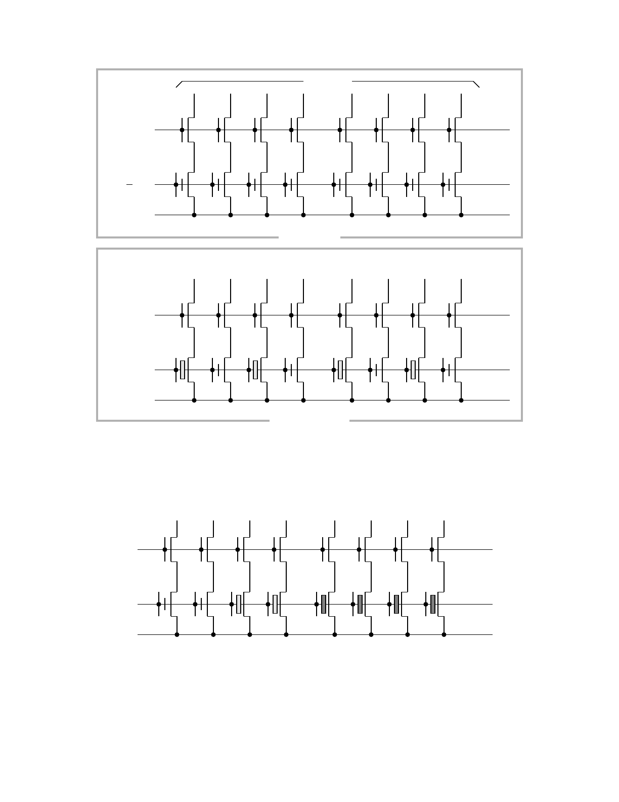
MOTOROLA ON-CHIP MEMORY M68HC11
4-24 REFERENCE MANUAL
Figure 4-8 Erase-Before-Write Programming Method
Figure 4-9 Program-More-Zeros Programming Method
Figure 4-10 shows the selective-write method being used to change an EEPROM lo-
ARRAY GROUND
7
VPP
NOT DRIVEN
654 3210
VTN
VSS
VPP
ERASE FIRST
ARRAY GROUND
7
VPP
654 3210
VSS
THEN PROGRAM $55 (NOT DRIVEN)
0101 0101
VPP VDD VPP VDD VPP VDD VPP VDD
ARRAY GROUND
7
VPP
654 3210
VSS
(NOT DRIVEN)
10 0 0
VDD VPP VPP VPP
1
VDD
0
VPP
00
VPP VPP
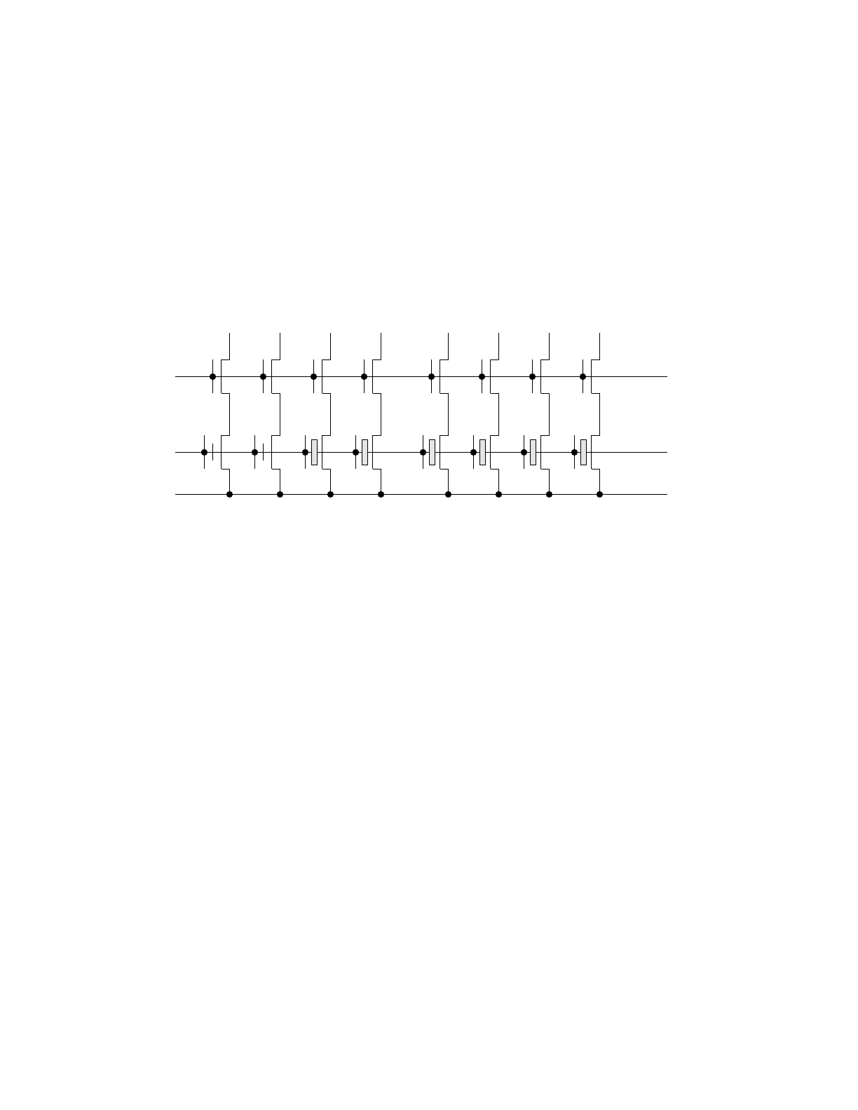
M68HC11 ON-CHIP MEMORY MOTOROLA
REFERENCE MANUAL 4-25
cation from $F0 to $C0. The calculated data pattern, $CF, was written to the location
during this programming operation (note the data pattern and voltage levels across the
top of the diagram). The floating gates are highlighted for the bits that should be pro-
grammed to zero after the operation. The floating gates of the programmed bits are
positively charged so these floating-gate transistors conduct, which introduces an in-
teresting question. For bits [3:0], there is a conductive path from VDD to the array
ground node. After programming, bits 4 and 5 have a conductive path from VPP to the
array ground node. Since there is effectively a conductive path from VDD to VPP, how
does the selective-write method work? Experimental results for this method are good;
however, additional study is required.
Figure 4-10 Selective-Write Programming Method
The production testing failure provides some additional information about the selec-
tive-write method but does not answer all the questions. Figure 4-11 shows the volt-
ages driving the EEPROM bits during the production test failure. The location was
previously programmed to $0D, as indicated by the highlighted floating gates. The bit
pattern and voltages across the top of Figure 4-11 reflect the $FC value that was writ-
ten to the location during this programming operation. This programming operation
was expected to cause bit 0 to be programmed, but the operation failed (indicated by
the bit 0 floating gate not highlighted). This operation fails because there is already a
conductive path from VDD to VPP at the start of the programming operation. Since the
weak VPP supply is shunted to VDD, no programming can occur.
The failure of the composite programming case verifies that the conductive paths exist
from VDD to the array ground and from VPP to the array ground. The failure also shows
that these conductive paths are capable of shunting VPP to a low enough level to pre-
vent programming.
VPP comes from a charge pump having very little drive-current capability. It is not very
surprising that VPP could be effectively shorted to VDD without producing any notice-
able load to VDD. In the selective-write method (see Figure 4-10), the path from VDD
to the array ground is conductive from the beginning of the operation. The path from
VPP to the array ground (through the bits being programmed) does not become con-
ductive until these floating gates are charged to a high enough positive level for the
ARRAY GROUND
7
VPP
654 3210
VSS
(NOT DRIVEN)
10 1 1
VDD VPP VDD VDD
11
VDD VDD
0
VPP
1
VDD
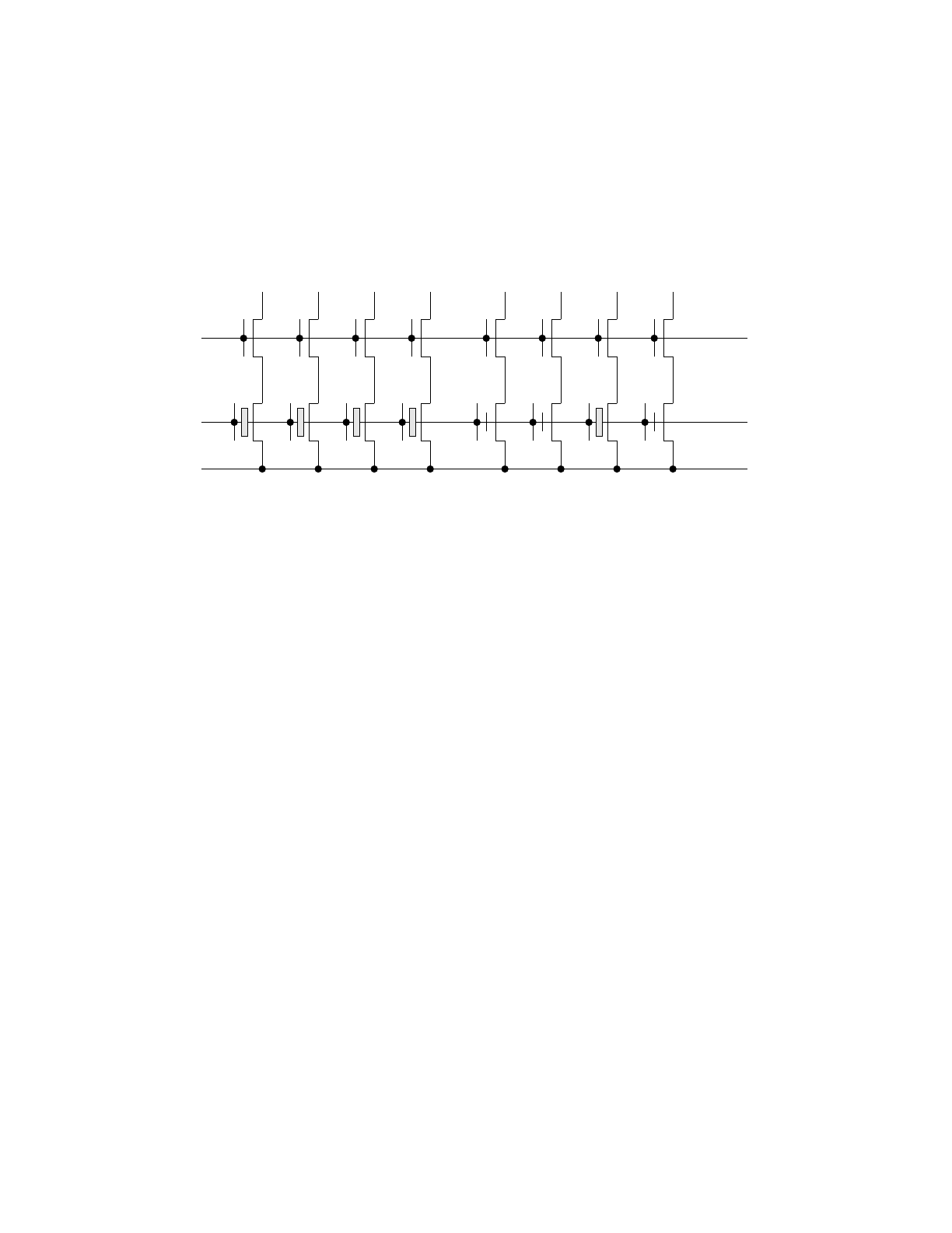
MOTOROLA ON-CHIP MEMORY M68HC11
4-26 REFERENCE MANUAL
floating-gate transistor to become conductive. It may be that the shunting path does
not develop until the bits have already finished programming. If two or more new bits
are being programmed and one were to become programmed (conductive) before the
other(s), VPP might become shunted before the other bit(s) could finish being pro-
grammed. One possible reason this unequal programming problem does not arise is
because the bits in a byte are so physically close to each other that they should have
nearly identical properties.
Figure 4-11 Composite Programming Method
The selective-write method may result in soft programming. The shunt path may de-
velop so late in the programming process that the bits are programmed well enough
to be read back as ones but not well enough to provide reliable data retention. On the
other hand, soft programming might be beneficial by limiting the stress on the thin ox-
ides. The selective-write strategy should be viewed with skepticism until additional
study can prove it has merit.
In most cases, EEPROM locations are only exposed to a few write-erase cycles in the
lifetime of a product. In some applications, a few variables need to endure several hun-
dred thousand write-erase cycles (e.g., the odometer reading in an automobile). Since
only a few variables require these extended write-erase cycle lifetimes, it is practical
to consider solutions involving the use of multiple EEPROM locations for the storage
of each such variable. Using an EEPROM location as an ordinary binary counter is
perhaps the worst case for EEPROM wear-out because the least significant bit toggles
at every count; thus, the EEPROM location must be erased and reprogrammed at
each count and is exposed to one write-erase cycle for every two counts.
A count value could be encoded so that an EEPROM location could be programmed
eight times by the program-more-zeros method before it has to be erased. In such a
scheme, the EEPROM location would only experience one write-erase cycle every
eight counts. This scheme of bit-position coding would only be needed for the low-or-
der bits of a counter since the high-order bits change much less frequently.
To extend the write-erase lifetime of a variable even further, using multiple EEPROM
locations would allow switching to a different location when the current location ap-
proached wear-out. The problem is to decide when a location is approaching wear-out.
ARRAY GROUND
7
VPP
654 3210
VSS
(NOT DRIVEN)
00 1101
VDD VDD VPP
VDD VPP
VDD
00
VDD VDD

M68HC11 ON-CHIP MEMORY MOTOROLA
REFERENCE MANUAL 4-27
Counting the number of times the location has been changed has two problems. First,
there is no good way of storing the usage count in EEPROM without wearing out the
usage count location in the same way as the location being monitored. Second, if
10,000 is used as the nominal life-expectancy number, the user may actually wear out
the location sooner than expected and fail, or he may not actually be using the location
to its potential. The life expectancy is approximately 100,000 write-erase cycles at
55°C even though it is only 5,000 at 125°C.

MOTOROLA ON-CHIP MEMORY M68HC11
4-28 REFERENCE MANUAL

M68HC11 RESETS AND INTERRUPTS MOTOROLA
REFERENCE MANUAL 5-1
SECTION 5
RESETS AND INTERRUPTS
Reset and interrupt operations are often discussed together because they share the
common concept of vector fetching to force a new starting point for further central pro-
cessing unit (CPU) operations. The reset structure in the MC68HC11A8, which is quite
different from other MCUs, is presented in this section. This reset system can generate
a reset output if reset-causing conditions are detected by internal systems. The on-
chip electrically erasable programmable read-only memory (EEPROM) also places
extra demands on external circuitry connected to the RESET pin.
The MC68HC11A8 includes 18 separate interrupt sources. On-chip peripheral sys-
tems generate maskable interrupts, which are recognized only if the global interrupt
mask bit (I) in the condition code register (CCR) is clear. Three interrupt sources con-
sidered non-maskable will be discussed in detail in this section.
Maskable interrupts are prioritized according to a default arrangement; however, any
one source may be elevated to the highest maskable priority position by a software-
accessible control register. This highest priority interrupt (HPRIO) register may be writ-
ten at any time provided the I bit in the CCR is set.
When interrupt conditions occur in an on-chip peripheral system, an interrupt status
flag is set to indicate the condition. When the user’s program has properly responded
to this interrupt request, the status flag must be cleared. The method of clearing varies
from one system to another, depending on the requirements of the system. The vari-
ous flag clearing methods and considerations are discussed in 5.7 Interrupts from In-
ternal Peripheral Subsystems.
5.1 Initial Conditions Established During Reset
Reset is used to force the microcontroller unit (MCU) to assume a set of initial condi-
tions and to begin executing instructions from a predetermined starting address. For
most practical applications, the initial conditions take effect almost immediately after
applying an active-low level to the RESET pin. Some reset conditions cannot take ef-
fect until/unless a clock is applied to the external clock input (EXTAL) pin. One exam-
ple is port B, which acts as an address output port in the expanded modes and as a
general-purpose output port in the single-chip modes. During reset in expanded mode,
these pins would be $FF because this is the high-order half of $FFFE. During reset in
single-chip mode, these pins would be $00. Since the mode pins are pipelined into the
MCU, a clock is needed for the MCU to recognize the mode selected.
If no clock is present, the port B pins could be in the wrong state due to the inability of
the MCU to recognize the correct mode of operation. If no clock is present, the MCU
cannot advance out of the reset condition since internal reset is a clocked sequence;
thus, the MCU cannot advance past the first step of this sequence. Even with no clock
present, a RESET signal will cause some changes. Most important, an unclocked RE-

MOTOROLA RESETS AND INTERRUPTS M68HC11
5-2 REFERENCE MANUAL
SET signal resets the clock divider circuitry so the on-chip oscillator will start. If an ap-
plication includes external clock circuitry driving the EXTAL pin, the RESET signal
should force this external clock to resume oscillation.
5.1.1 System Initial Conditions
Once the reset condition is recognized, internal registers and control bits are forced to
an initial state. These initial states, in turn, control on-chip peripheral systems to force
them to known start-up states. Most of the initial conditions are independent of the op-
erating mode. The following paragraphs summarize the initial conditions of the MCU
as it leaves reset.
5.1.1.1 CPU
After reset, the CPU fetches the restart vector from locations $FFFE,FFFF
($BFFE,BFFF if in special test or bootstrap mode) during the first three cycles and be-
gins executing instructions. The stack pointer and other CPU registers are indetermi-
nate immediately after reset; however, the X and I interrupt mask bits in the CCR are
set to mask any interrupt requests. Also, the S bit in the CCR is set to disable the
STOP mode.
5.1.1.2 Memory Map
After reset, the RAM and I/O mapping (INIT) register is initialized to $01, putting the
256 bytes of random-access memory (RAM) at locations $0000–$00FF and the con-
trol registers at locations $1000–$103F. The 8-Kbyte read-only memory (ROM) and/
or the 512-byte EEPROM may or may not be present in the memory map because the
two bits that enable them in the configuration control (CONFIG) register are EEPROM
cells not affected by reset or power-down.
5.1.1.3 Parallel I/O
When a reset occurs in expanded-multiplexed operating mode, the 18 pins used for
parallel I/O are dedicated to the expansion bus. If a reset occurs in the single-chip op-
erating mode, the strobe A flag (STAF), strobe A interrupt (STAI), and handshake
(HNDS) control bits in the parallel input/output control (PIOC) register are cleared so
that no interrupt is pending or enabled, and the simple strobed mode (rather than full-
handshake mode) of parallel I/O is selected. The port C wired-OR mode (CWOM) bit
in PIOC is cleared. Port C is initialized as an input port (data direction register for port
C, DDRC $00); port B is a general-purpose output port with all bits cleared. STRA is
the edge-sensitive strobe A input, and the active edge is initially configured to detect
rising edges (edge select for strobe A (EGA) bit in PIOC is set). Port C, port D (bits
[5:0]), port A (bits 0, 1, 2, and 7), and port E are configured as general-purpose high-
impedance inputs. Port B and bits [6:3] of port A have their directions fixed as outputs,
and their reset state is logic zero.
5.1.1.4 Timer
During reset, the timer system is initialized to a count of $0000. The prescaler bits are
cleared, and all output-compare registers are initialized to $FFFF. All input-capture

M68HC11 RESETS AND INTERRUPTS MOTOROLA
REFERENCE MANUAL 5-3
registers are indeterminate after reset. The output-compare 1 (OC1M) mask register
is cleared so that successful OC1 compares do not affect any I/O pins. The other four
output compares are configured to not affect any I/O pins on successful compares. All
three input-capture edge-detector circuits are configured for capture-disabled opera-
tion. The timer overflow interrupt flag and all eight timer function interrupt flags are
cleared. All nine timer interrupts are disabled since their mask bits are cleared.
5.1.1.5 Real-Time Interrupt
The real-time interrupt flag is cleared, and automatic hardware interrupts are masked.
The rate control bits are cleared after reset and may be initialized by software before
the real-time interrupt system is used.
5.1.1.6 Pulse Accumulator
The pulse accumulator system is disabled at reset so that the pulse accumulator input
(PAI) pin defaults to being a general-purpose input pin.
5.1.1.7 COP Watchdog
The computer operating properly (COP) watchdog system is enabled if the NOCOP
control bit in the CONFIG register (EEPROM cell) is clear and disabled if NOCOP is
set. The COP rate is set for the shortest duration time-out.
5.1.1.8 Serial Communications Interface (SCI)
The reset condition of the SCI system is independent of the operating mode. At reset,
the SCI baud rate is indeterminate and must be established by a software write to the
BAUD register. All transmit and receive interrupts are masked, and both the transmit-
ter and receiver are disabled so the port pins default to being general-purpose I/O
lines. The SCI frame format is initialized to an 8-bit character size. The send break and
receiver wake-up functions are disabled. The transmit data register empty (TDRE) and
transmit complete (TC) status bits in the SCI status register are both set, indicating that
there is no transmit data in either the transmit data register or the transmit serial shift
register. The receive data register full (RDRF), IDLE, overrun (OR), and framing error
(FE) receive-related status bits are all cleared. Upon reset in special bootstrap mode,
execution begins in the 192-byte bootstrap ROM, which changes some of the initial
conditions by the time the bootloading process is finished. This firmware sets port D
to wired-OR mode, establishes a baud rate, and enables the SCI receiver and trans-
mitter.
5.1.1.9 Serial Peripheral Interface (SPI)
The SPI system is disabled by reset. The port pins associated with this function default
to being general-purpose I/O lines.
5.1.1.10 Analog-to-Digital (A/D) Converter
The A/D converter system configuration is indeterminate after reset. The conversion
complete flag is cleared by reset. The A/D power-up (ADPU) bit is cleared by reset,
disabling the A/D system.

MOTOROLA RESETS AND INTERRUPTS M68HC11
5-4 REFERENCE MANUAL
5.1.1.11 Other System Controls
The EEPROM programming controls are all disabled so the memory system is config-
ured for normal read operation. The highest priority I bit interrupt defaults to being the
external interrupt request (IRQ) pin by PSEL[3:0] equal to 0:1:0:1. The IRQ pin is con-
figured for level-sensitive operation (for wired-OR systems). The read bootstrap ROM
(RBOOT), special mode (SMOD), and mode A (MDA) bits in the HPRIO register reflect
the status of the mode B (MODB) and MODA inputs at the rising edge of reset. The
enable oscillator start-up delay (DLY) control bit is set to specify that an oscillator start-
up delay is imposed upon recovery from STOP mode. The clock monitor system is dis-
abled by clock monitor enable (CME) equals zero.
The MC68HC11A8 has three internal sources that can cause reset as well as the ex-
ternal application of a low level to the RESET pin. No matter which of these sources
causes reset, the entire MCU is reset. The RESET pin is driven low as a result of any
of the reset sources. The only distinction that is made between the causes of reset is
the reset vector, which is used to tell the CPU the starting address for execution when
reset is released.
A few registers are not forced to a start-up condition as a result of reset. Since these
registers do not affect the starting conditions at MCU pins, it is not important to force
them to a start-up state during reset. One such example is the main-timer input-cap-
ture registers. Since these registers are not useful until after an input capture occurs,
it is not important to force them to a start-up state during reset.
5.1.2 CONFIG Register Allows Flexible Configuration
The M68HC11 includes a nonvolatile CONFIG register, which controls a number of
options typically controlled by mask options or by additional mode selection choices in
other MCUs. By using a nonvolatile EEPROM-based register, it is possible to achieve
the same effects as if the options were mask programmed and, at the same time, allow
users to change these features after the MCU is manufactured. The most important
aspect of this method of selecting options is that the selections automatically take ef-
fect on any power-up or reset without any software intervention. Two classes of fea-
tures can be controlled in this manner. First, there are configuration choices that must
inherently be made before the reset vector is even fetched. For example, the ROM en-
able must be decided so that the reset vector can be fetched out of the correct memory
as the MCU comes out of reset. The COP watchdog timer enable is an example of the
second class of features that can be controlled by an EEPROM bit. The COP watch-
dog timer is intended to detect software failures; thus, it is important to enable or dis-
able this feature without any software intervention. If software could disable or was
required to enable the COP watchdog, the COP watchdog timer could not detect a fail-
ure of that software.
The CONFIG register controls the presence or absence of ROM and/or EEPROM, en-
ables/disables the COP watchdog timer, and engages/disengages the security option.
The CONFIG register and mechanism are described in greater detail in 3.2.1 Opera-
tion of CONFIG Mechanism. The features enabled by the CONFIG register can be
thought of as mask-programmed options that do not require software service.

M68HC11 RESETS AND INTERRUPTS MOTOROLA
REFERENCE MANUAL 5-5
5.1.3 Mode of Operation Established
During reset, the basic mode of operation is established, which determines whether
the MCU will operate as a self-contained single-chip system or as an expanded sys-
tem that includes external memory resources. There are also special variations of
these two basic modes of operation. The bootstrap mode is the special variation of the
normal single-chip mode, and the special test mode is the special variation of the nor-
mal expanded mode. The levels on the two mode select pins during reset determine
which of these four modes of operation will be selected.
The hardware mode select mechanism begins with the logic levels on the MODA and
MODB pins while the MCU is in the reset state. The logic levels on the MODA and
MODB pins are fed into the MCU via a clocked pipeline path. The captured levels will
be those that were present part of a clock cycle before the RESET pin rose. This fact
assures a zero hold-time requirement on the mode select pins relative to the rising
edge at the RESET pin. The captured levels determine the logic state of the SMOD
and MDA control bits in the HPRIO register. These two control bits actually control the
logic circuits involved in hardware mode selection. Table 5-1 summarizes the opera-
tion of the mode pins and mode control bits.
5.1.4 Program Counter Loaded with Reset Vector
As reset is released, the CPU program counter is loaded with the reset vector that
points to the first instruction in the user’s program. Depending on the cause of reset
and the mode of operation, the reset vector may be fetched from any of six possible
locations. In older Motorola MCUs, there was only one reset vector at $FFFE,FFFF.
5.2 Causes Of Reset
In the MC68HC11A8, there are on-chip systems that can detect MCU system failures
and generate a low level out the RESET pin to reinitialize other peripherals in the sys-
tem. To distinguish between these causes, separate reset Vectors are used. The pri-
mary reset vector is used when the cause of reset is the internal power-on reset circuit
or application of a low level to the RESET pin. In normal expanded and normal single-
chip modes, this vector is located at $FFFE,FFFF. If the oscillator input stops or is run-
ning too slow, the clock monitor circuit will generate a reset (provided the clock monitor
is enabled). Time-out of the internal COP watchdog timer will generate a reset (provid-
ed the COP system is enabled). Table 5-2 summarizes the reset-vector locations ver-
sus the cause of reset and mode of operation.
Table 5-1 Hardware Mode Select Summary
Inputs Mode Description Control Bits in HPRIO (Latched at Reset)
MODB MODA RBOOT SMOD MDA Inputs
10
Normal Single
Chip 0000
1 1 Normal Expanded 0000
0 0 Special Bootstrap 0010
0 1 Special Test 0111

MOTOROLA RESETS AND INTERRUPTS M68HC11
5-6 REFERENCE MANUAL
In special test and bootstrap modes, MCU vectors are located at $BFC0–$BFFF rath-
er than the normal $FFC0–$FFFF area. The primary reason for this change is to be
sure the reset vector can be supplied from an external source in special test mode.
The normal reset vector is located at $FFFE,FFFF, which can be internal ROM or ex-
ternal memory space (depending on whether the internal ROM is enabled). The spe-
cial test mode reset vector is at $BFFE,BFFF, which is always an external access
independent of other system conditions.
This alternate mapping is important to the operation of bootstrap mode because it al-
lows reset and other vectors to be located within the 192-byte bootloader ROM. As the
MCU comes out of reset in special bootstrap mode, the reset vector is fetched out of
the bootloader ROM, and execution begins at the start of the bootloader program.
While in bootstrap mode, interrupts can be vectored to locations in the bootloaded pro-
gram in RAM rather than vectoring to the routines specified in the internal ROM pro-
gram.
The M68HC11 MCU is capable of distinguishing between an external reset and resets
from the internal COP and clock monitor systems. When the COP watchdog timer
times out or the clock monitor detects a clock failure, the COP and clock monitor status
is temporarily saved. The RESET pin is then driven low for about four E-clock cycles
and is released. Two E-clock cycles later, the RESET input is sampled. If RESET is
high (has risen to logic one within the two cycles since it was released), the source of
reset is presumed to be either the COP or clock monitor system. If RESET is still low,
the source is presumed to be an external reset request, and the temporarily saved sta-
tus from the COP and clock monitor systems is erased. Although there would rarely
be more than one cause for a particular reset sequence, the three reset vectors are
prioritized. If an external reset request drives the RESET pin low for less than four E-
clock cycles, the differentiation logic could assume the source of reset was the internal
COP or clock monitor system; however, as long as neither of these causes was indi-
cated by the temporarily latched status, the normal reset vector would still be used by
default. Although this MCU can differentiate between different reset causes, the most
common implementation would direct all reset vectors to the same initialization soft-
ware, regardless of the cause of reset.
There are four possible sources of reset in the MC68HC11A8. An internal circuit de-
tects the rising edge on VDD and initiates a power-on reset. An on-chip COP watchdog
timer monitors proper software execution; if software does not service this timer within
its time-out period, a system reset is generated. Another on-chip circuit monitors the
MCU clock frequency. If the MCU clock stops or is running too slow, a system reset is
generated. Finally, a user can initiate an external reset by momentarily driving the RE-
SET pin low. The COP and clock monitor features can be disabled. The power-on re-
Table 5-2 Reset Vector vs. Cause and MCU Mode
Cause of Reset Normal Mode Vector Special Test or Bootstrap Vector
POR or RESET Pin $FFFE,FFFF $BFFE,BFFF
Clock Monitor Fail $FFFC,FFFD $BFFC,BFFD
COP Watchdog Time-Out $FFFA,FFFB $BFFA,BFFB

M68HC11 RESETS AND INTERRUPTS MOTOROLA
REFERENCE MANUAL 5-7
set and external reset share the normal reset vector; whereas, the COP and clock
monitor reset each have their own vector. The four causes of reset are described in
greater detail in the following paragraphs.
5.2.1 Power-On Reset (POR)
The POR is only intended to initialize internal MCU circuits. As VDD is applied to the
MCU, the POR circuit triggers and initiates a reset sequence. POR triggers an internal
timing circuit that holds the RESET pin low for 4064 cycles of the internal PH2 clock.
The MCU does not advance past this reset condition until a clock is present at the EX-
TAL pin long enough for these 4064-cycle PH2 clocks to be detected. The internal
POR circuit will not retrigger unless VDD has discharged to 0 V; therefore, the internal
POR circuit is not suitable as a power-loss detector.
In almost all M68HC11 systems, there will be an external circuit to hold the RESET pin
low whenever VDD is below normal operating level. This external voltage-level detec-
tor or other external reset circuits are the normal source of reset in a system; the inter-
nal POR circuit only serves to initialize internal control circuitry during cold starts.
In some unusual applications, it may be desirable to hold RESET low long enough for
the oscillator to reach stable operating frequency. This stable operating frequency is
not a requirement of the MCU because the M68HC11 is a fully static design, which can
operate correctly even when the oscillator has not reached stable operating frequency.
If the oscillator has not reached stable operating frequency by the time RESET is re-
leased, software and timed delays will be longer than expected since these delays are
based on the oscillator frequency. In most applications, such errors within the first few
milliseconds of operation are of no concern, and no external power-on delay is neces-
sary. In cases where timing is critical immediately out of RESET, an external POR cir-
cuit must be provided. The required amount of delay depends upon the oscillator
startup time, which varies with the frequency and design of the oscillator as well as
such things as VDD rise time. In a typical M68HC11 design with an E-clock frequency
of 2 MHz, the internal POR will only hold RESET low for about 2 ms after oscillator
start. With an 8-MHz crystal, the M68HC11 oscillator will typically start when VDD
reaches about 1 V. For a typical VDD rise time, the internal POR times out well before
VDD reaches an acceptable level. Thus, POR alone is rarely able to provide for all re-
set needs, and some external reset circuitry will be required.
5.2.2 COP Watchdog Timer Reset
The COP watchdog timer system is intended to detect software processing errors.
When the COP is being used, software is responsible for keeping a free-running
watchdog timer from timing out. If the watchdog timer times out, it is an indication that
software is no longer being executed in the intended sequence; thus, a system reset
is initiated.
The COP system is enabled or disabled, depending on the state of the NOCOP bit in
the CONFIG register. This enable is like a mask option in that it is effective immediate-
ly out of reset and is not dependent on any software action. Unlike a programmed
mask option, the COP enable may be changed by the end user. The requirements for

MOTOROLA RESETS AND INTERRUPTS M68HC11
5-8 REFERENCE MANUAL
changing the enable bit are designed so the NOCOP bit is very unlikely to be changed
by accident in the end system. The only way to change the enable status of the COP
system is to change the contents of the EEPROM-based CONFIG register. Even after
the NOCOP bit is changed, the MCU must be reset before the new status becomes
effective. In the special test and bootstrap operating modes, the COP system is initially
inhibited by the disable resets (DISR) control bit in the TEST1 register. The DISR bit
can be written to zero to enable COP resets while the MCU is in special test or boot-
strap operating mode.
The COP time-out period is set by the COP timer rate control bits (CR1 and CR0) in
the configuration options (OPTION) register. After reset, these bits are both zero,
which selects the fastest time-out period. The MCU internal E clock is first divided by
215 before it enters the COP watchdog system. The CR1 and CR0 bits control a further
scaling factor for the watchdog timer (see Table 5-3). The columns at the right of the
table show the resulting watchdog time-out periods for three typical oscillator frequen-
cies. In normal operating modes, these bits can only be written once, and that write
must be within 64 bus cycles after reset.
The COP timer must be reset by a software sequence prior to time-out to avoid a COP
reset. The software COP reset is a two-step sequence. The first step is to write $55 to
the COPRST register to arm the COP timer-clearing mechanism. The second step is
to write $AA to the COPRST register, which clears the COP timer. Any number of in-
structions can be performed between these two steps as long as both steps are per-
formed in the correct sequence before the timer times out. This reset sequence is
sometimes referred to as servicing the COP timer.
Since the COP timer is based on the MCU clock, the COP watchdog cannot detect er-
rors that cause the MCU clock to stop. The clock monitor system (see 5.2.3 Clock
Monitor Reset) can be used as a backup for COP to force a system reset if the MCU
clocks stop.
Placing the COP service instructions in an interrupt service routine is bad practice. In
such a case, the interrupt could occur often enough to keep the COP system satisfied
even if the main-line program was no longer functioning.
The implementation of the COP timer causes a tolerance on the time-out period. The
Table 5-3 Watchdog Rates vs. Crystal Frequency
CR1 CR0 E÷215 Divided By
Crystal Frequency
223 Hz 8 MHz 4 MHz
Nominal Time-Out
0 0 1 15.625 ms 16.384 ms 32.768 ms
0 1 4 62.5 ms 65.536 ms 131.07 ms
1 0 16 250 ms 262.14 ms 524.29 ms
1 1 64 1 s 1.049 s 2.1 s
2.1 MHz 2 MHz 1 MHz
Bus Frequency (E clock)

M68HC11 RESETS AND INTERRUPTS MOTOROLA
REFERENCE MANUAL 5-9
E divided by 215 clock into the COP system is free-running and, for practical purposes,
is asynchronous to the COP service software. All additional divider stages in the COP
timer are reset each time the COP service sequence is performed. There is an uncer-
tainty about when the first E divided by 215 clock will reach the COP timer stages. This
uncertainty causes the specified time-out period to have a tolerance of minus zero to
plus one cycle of the E divided by 215 clock. This tolerance varies with E-clock frequen-
cy but does not change with respect to the COP rate selected by the CR1 and CR0
bits. Figure 10-3 and 10.2.3 COP Watchdog Function contain additional information
about this clocking structure.
5.2.3 Clock Monitor Reset
The clock monitor circuit is based on an internal resistor-capacitor (RC) time delay. If
no MCU clock edges are detected within this RC time delay, the clock monitor can op-
tionally generate a system reset. The clock monitor function is enabled/disabled by the
CME control bit in the OPTION register. This time-out is based on an RC delay so that
the clock monitor can operate without any MCU clocks.
Processing variations cause the RC time-out to vary somewhat from lot to lot and part
to part. An E-clock frequency below 10 kHz will definitely be detected as a clock mon-
itor error. An E-clock frequency of 200 kHz or more will prevent clock monitor errors.
Any system operating below 200 kHz E-clock frequency should not use the clock mon-
itor function.
When the clock monitor is enabled and the MCU clocks slow down or stop, a system
reset is generated. The bidirectional RESET pin is driven low to reset the external sys-
tem and the MCU. Clock monitor has a separate reset vector from COP reset and ex-
ternal reset to enable software to determine the cause of reset. While the MCU is in
special test or bootstrap mode, resets from the COP and clock monitor systems are
initially disabled by a one in the DISR bit in the TEST1 register. While still in the special
operating modes, COP and clock monitor resets can be re-enabled by writing the
DISR control bit to zero. In normal operating modes, the DISR bit is forced to zero and
cannot be set to one.
Clock monitor is often used as a backup for the COP watchdog system. Since the COP
needs a clock to function, it is unable to function if the clocks stop. In such a case, the
clock monitor system could detect clock failures not detected by the COP system.
Another use for the clock monitor is to protect against the unintentional execution of
the STOP instruction. Some applications view the STOP instruction as a serious prob-
lem because it causes MCU clocks to stop, thus disabling all software execution and
on-chip peripheral functions. A stop disable bit (S) in the CCR is the first line of defense
against unwanted STOP instructions. While the S bit is one, the STOP instruction acts
as a no-operation (NOP) instruction, which does not interfere with MCU clock opera-
tion. Clock monitor can provide an additional level of protection by generating a sys-
tem reset if the MCU clocks are accidentally stopped.
It is possible to use the clock monitor in systems that also use the STOP instruction.
In such a system, the CME control bit would be written to zero to disable the clock

MOTOROLA RESETS AND INTERRUPTS M68HC11
5-10 REFERENCE MANUAL
monitor prior to executing an intentional STOP instruction. After recovery from STOP,
the CME bit would be written to one to enable the clock monitor during normal execu-
tion.
The reset sequence is a clocked operation; whereas, clock monitor resets are gener-
ated when the clocks stop. In many cases, the low level on RESET will correct the
cause of the stopped MCU clocks, and recovery can proceed much as in the COP re-
set case. In cases where the MCU clocks do not resume as a result of the clock mon-
itor reset, the driven low level at the RESET pin will remain indefinitely.
5.2.4 External Reset
In addition to the internal sources, reset can be forced by applying a low level to the
RESET pin. The resulting reset sequence is identical to the internal causes. Upon rec-
ognition of the reset request, internal logic turns on an internal N-channel device,
which actively holds the RESET pin low for about four cycles. In a normal system, the
external source of RESET would be redundantly driving the pin low during this time
and would continue to hold the pin low longer than this four cycles. Two E-clock cycles
after the internal N-channel driver releases the pin, the RESET pin is sampled. A low
level at this time indicates the reset was caused by some external source. When the
RESET pin is eventually released, the normal reset vector is fetched and processing
begins.
In all cases of reset, the internal N-channel device holds the RESET pin low for at least
four E-clock cycles. All resets cause internal registers and on-chip peripherals to be
re-initialized. The only difference between causes of reset is the vector locations used.
In the abnormal case where the RESET pin is not held low long enough to be detected
as the cause, the reset is tentatively assumed to have come from the COP or clock
monitor systems. Priority logic assigns highest priority to the clock monitor and second
highest priority to the COP watchdog. If neither of these sources is pending, the normal
reset vector is selected by default. In another abnormal case where the RESET line is
loaded by too much capacitance to rise within two cycles after the internal N-channel
turns off, there will be no way for the internal logic to discriminate between an internal
or external reset source; thus, all resets are interpreted as external requests.
Figure 5-1 shows an example of an external reset circuit. The low voltage inhibit (LVI)
device [1] holds RESET low whenever VDD is below operating level. The LVI device
[2] and the RC on its input provide an external POR delay. The switch [3] provides for
manual reset. Voltage detectors [1] and [2] have open-drain outputs, and the pull-up
resistor holds the RESET pin high unless either voltage detector or the internal MCU
reset circuitry drives the RESET pin low. The LVI circuit [1] (or some equivalent circuit)
is required for virtually all M68HC11 systems. The external POR delay and manual re-
set switch are optional. For many applications, the voltage detector [1] and the pull-up
resistor [4] are the only external components needed for reset.
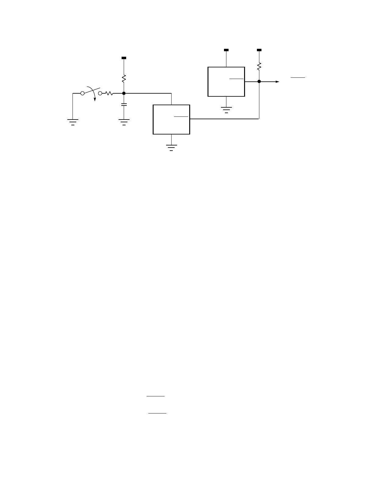
M68HC11 RESETS AND INTERRUPTS MOTOROLA
REFERENCE MANUAL 5-11
Figure 5-1 Typical External Reset Circuit
5.3 Interrupt Process
The CPU in a microcontroller sequentially executes instructions. In many applications,
it is necessary to execute sets of instructions in response to requests from various pe-
ripheral devices. These requests are often asynchronous to the execution of the main
program. Interrupts provide a way to temporarily suspend normal program execution
so the CPU can be freed to service these requests. After an interrupt has been ser-
viced, the main program resumes as if there had been no interruption.
The instructions executed in response to an interrupt are called the interrupt service
routine. These routines are much like subroutines except that they are called through
the automatic hardware interrupt mechanism rather than by a subroutine call instruc-
tion, and all CPU registers are saved on the stack rather than just saving the program
counter. An interrupt (provided it is enabled) causes normal program flow to be sus-
pended as soon as the currently executing instruction finishes. The interrupt logic then
pushes the contents of all CPU registers onto the stack so the CPU context can be
restored after the interrupt is finished. After stacking the CPU registers, the vector for
the highest priority pending interrupt source is loaded into the program counter, and
execution continues with the first instruction of the interrupt service routine. An inter-
rupt is concluded with a return from interrupt (RTI) instruction, which causes all CPU
registers and the return address to be recovered from the stack so that the interrupted
program can resume as if there had been no interruption.
Interrupts can be enabled or disabled by mask bits (X and I) in the CCR and by local
enable mask bits in the on-chip peripheral control registers. A few important interrupt
sources that are always enabled are called non-maskable interrupts. The non-
maskable interrupt request (XIRQ) pin is effectively a non-maskable interrupt source
except that it is disabled immediately after reset. Very special logic is associated with
the interrupt mask bit (X) for XIRQ in the CCR to overcome classic problems associ-
ated with a non-maskable interrupt while allowing all of the benefits of such an inter-
rupt. The remaining interrupt sources are maskable by the interrupt mask bit (I) in the
4.7 kΩ
3
1
2
3
1
2
[4]
[3]
[2]
[1] TO RESET
VDD
MC34064
RESET
GND
IN
OF M68HC11
RESET
GND
IN
MANUAL
RESET SWITCH
R1
C
MC34164
R2
VDD
VDD

MOTOROLA RESETS AND INTERRUPTS M68HC11
5-12 REFERENCE MANUAL
CCR.
The interrupt mask bits in the CCR provide a means of controlling the nesting of inter-
rupts. In rare cases, it may be useful to allow an interrupt routine to be interrupted
(nesting of interrupts). Nesting of interrupts is discouraged because it greatly compli-
cates a system and rarely improves system performance. By default, the interrupt
structure inhibits interrupts during the interrupt entry sequence by setting the interrupt
mask bit(s) in the CCR. As the CCR is recovered from the stack during the RTI instruc-
tion, the CCR bits return to the enabled state so additional interrupts can be serviced.
If nesting of interrupts is desired, it must be specifically allowed by clearing the inter-
rupt mask bit(s) after entering the interrupt service routine. Care must be taken to spe-
cifically mask (disable) the present interrupt with a local enable mask bit or to clear the
interrupt source flag before clearing the mask bit in the CCR; otherwise, the same
source would immediately interrupt, and an infinite loop could result.
Upon reset, both the X and I bit are set to inhibit all maskable interrupts and XIRQ.
After minimum system initialization, software may clear the X bit by a transfer accumu-
lator A to CCR (TAP) instruction, thus enabling XIRQ. Thereafter, software cannot set
the X bit; thus, an XIRQ is effectively a non-maskable interrupt. Since the operation of
the I-bit-related interrupt structure has no effect on the X bit, the external XIRQ pin re-
mains effectively non-maskable. In the interrupt priority logic, XIRQ is a higher priority
than any source that is maskable by the I bit. All I-bit-related interrupts operate normal-
ly with their own priority relationship. When an I-bit-related interrupt occurs, the I bit is
automatically set by hardware after stacking the CCR byte, but the X bit is not affected.
When an XIRQ occurs, both the X and I bits are automatically set by hardware after
stacking the CCR. An RTI instruction restores the X and I bits to their pre-interrupt re-
quest state.
5.3.1 Interrupt Recognition and Stacking Registers
An interrupt can be recognized at any time provided it is enabled by its local mask (if
any) and by the global mask bit in the CCR. Once any interrupt source is recognized,
the CPU will respond at the completion of the currently executing instruction. Instruc-
tions cannot be interrupted; rather, the CPU decides whether to fetch another instruc-
tion or process an interrupt. In calculating the latency time from the actual interrupt
request to the CPU response to that request, the user must consider the possibility that
the CPU had just started a long instruction as the interrupt was requested. Most in-
structions are two to four cycles long, but the multiply (MUL) and integer divide (IDIV)
or fractional divide (FDIV) instructions are 10 and 41 cycles, respectively.
When the CPU decides to service an interrupt, the contents of CPU registers are
pushed (stored) on the stack in the order PCL, PCH, IYL, IYH, IXL, IXH, ACCA, ACCB,
CCR. After the CCR value is stacked, the I bit in the CCR (and the X bit if XIRQ is
pending) is set to inhibit further interrupts. The interrupt sequence then proceeds to
the priority resolution step.
5.3.2 Selecting Interrupt Vectors
After the CCR has been stacked, the CPU evaluates all pending interrupt requests to

M68HC11 RESETS AND INTERRUPTS MOTOROLA
REFERENCE MANUAL 5-13
determine which source has the highest priority. Since the priority resolution step oc-
curs several cycles after the original decision to service an interrupt, a higher priority
source could become pending after the stacking operation started but before the pri-
ority is resolved. In such a case, the interrupt that is serviced can be different from the
source that initiated the interrupt sequence. This subtle aspect means that the latency
from an interrupt request to when it is serviced can be shorter than expected.
Interrupts obey a fixed hardware-priority circuit to resolve simultaneous requests; how-
ever, one I-bit-related interrupt source may be elevated to the highest I bit priority po-
sition in the resolution circuit. The first six interrupt sources are not masked by the I bit
in the CCR and have the fixed priority interrupt relationship: reset, clock monitor fail,
COP fail, illegal opcode, and XIRQ. Each of these sources is an input to the priority
resolution circuit. Software interrupt (SWI) is actually an instruction and has the high-
est priority other than reset because, once the SWI opcode is fetched, no other inter-
rupt can be honored until the SWI vector has been fetched. The highest I-bit-related
priority input is assigned under software control (of the HPRIO register) to be connect-
ed to any one of the remaining I-bit-related interrupt sources. To avoid timing races,
the HPRIO register may only be written while the I-bit-related interrupts are inhibited
(I bit in CCR = 1). An interrupt that is assigned to this highest priority position is still
subject to masking by any associated control bits or by the I bit in the CCR. The inter-
rupt vector address is not affected by assigning a source to this highest priority posi-
tion.
The following figure shows the HPRIO register. The HPRIO register may be read at
any time but may only be written under special circumstances. The high-order four bits
of HPRIO may only be written while the MCU is operating in one of the special modes
(SMOD = 1). The low-order four bits may only be written while the I bit in the CCR is
one.
RBOOT — Read Bootstrap ROM
Can be written only while SMOD equals one
1 = Bootstrap ROM enabled and located from $BF40–$BFFF
0 = Bootstrap ROM disabled and not present in memory map
The RBOOT control bit enables or disables the special bootstrap control ROM. This
192-byte mask-programmed ROM contains the firmware required to load a user’s pro-
gram through the SCI into the internal RAM and jump to the loaded program. In all
modes other than the special bootstrap mode, this ROM is disabled and does not oc-
cupy any space in the 64-Kbyte memory map. Although it is zero when the MCU
comes out of reset in test mode, the RBOOT bit may be written to one while in special
test mode.
SMOD — Special Mode
May be written to zero but not back to one
HPRIO — Highest Priority I-Bit Interrupt and Miscellaneous $103C
BIT 7 654321BIT 0
RBOOT SMOD MDA IRV PSEL3 PSEL2 PSEL1 PSEL0
RESET: (Refer to Table 5-1)

MOTOROLA RESETS AND INTERRUPTS M68HC11
5-14 REFERENCE MANUAL
1 = Special mode variation in effect
0 = Normal mode variation in effect
MDA — Mode A Select
Can be written only while SMOD equals one
1 = Normal expanded or special test mode in effect
0 = Normal single-chip or special bootstrap mode in effect
IRV — Internal Read Visibility
Can be written only while SMOD equals one; forced to zero if SMOD equals zero
1 = Data driven onto external bus during internal reads
0 = Data from internal reads not visible on expansion bus (levels on bus ignored)
The IRV control bit is used during factory testing and sometimes during emulation to
allow internal read accesses to be visible on the external data bus. Care is required to
avoid data bus contention while IRV is active because the bidirectional data bus is driv-
en out during reads of internal addresses, even though the R/W line suggests the data
bus is in the high-impedance read mode. In normal modes, this function is disabled;
thus, complex decode logic is not required to protect against accidental bus conflicts.
PSEL[3:0] — Priority Select Bits 3:0
Can be written only while I bit in CCR equals one. These four bits allow any one
maskable interrupt source to be elevated to the highest priority position. Non-
maskable interrupts still take priority over all maskable interrupts. The following table
shows the relationship between the PSEL[3:0] bit values and the interrupt source that
is promoted. The priority can only be changed while interrupts are masked (I bit in CCR
= 1) to avoid race conditions.
Figure 5-2,Figure 5-4, and Figure 5-6 illustrate the interrupt process as it relates to
Table 5-4 Highest Priority 1 Interrupt vs. PSEL[3:0]
PSEL3 PSEL2 PSEL1 PSEL0 Interrupt Source Promoted
0000Timer Overflow
0001Pulse Accumulator Overflow
0010Pulse, Accumulator Input Edge
0011SPI Transfer Complete
0100SCI Serial System
0101Reserved (Default to IRQ)
0110
IRQ (External Pin or Parallel I/O)
0111Real-Time Interrupt
1000Timer Input Capture 1
1010Timer Input Capture 2
1010Timer Input Capture 3
1011Timer Output Compare 1
1100Timer Output Compare 2
1101Timer Output Compare 3
1110Timer Output Compare 4
1111Timer Output Compare 5

M68HC11 RESETS AND INTERRUPTS MOTOROLA
REFERENCE MANUAL 5-15
normal processing. Figure 5-2 shows how the CPU begins from a reset and how in-
terrupt detection relates to normal opcode fetches. Figure 5-4, an expansion of a
block in Figure 5-2, shows how interrupt priority is resolved. Figure 5-6, an expansion
of the SCI interrupt block in Figure 5-4, shows the resolution of interrupt sources within
the SCI subsystem.
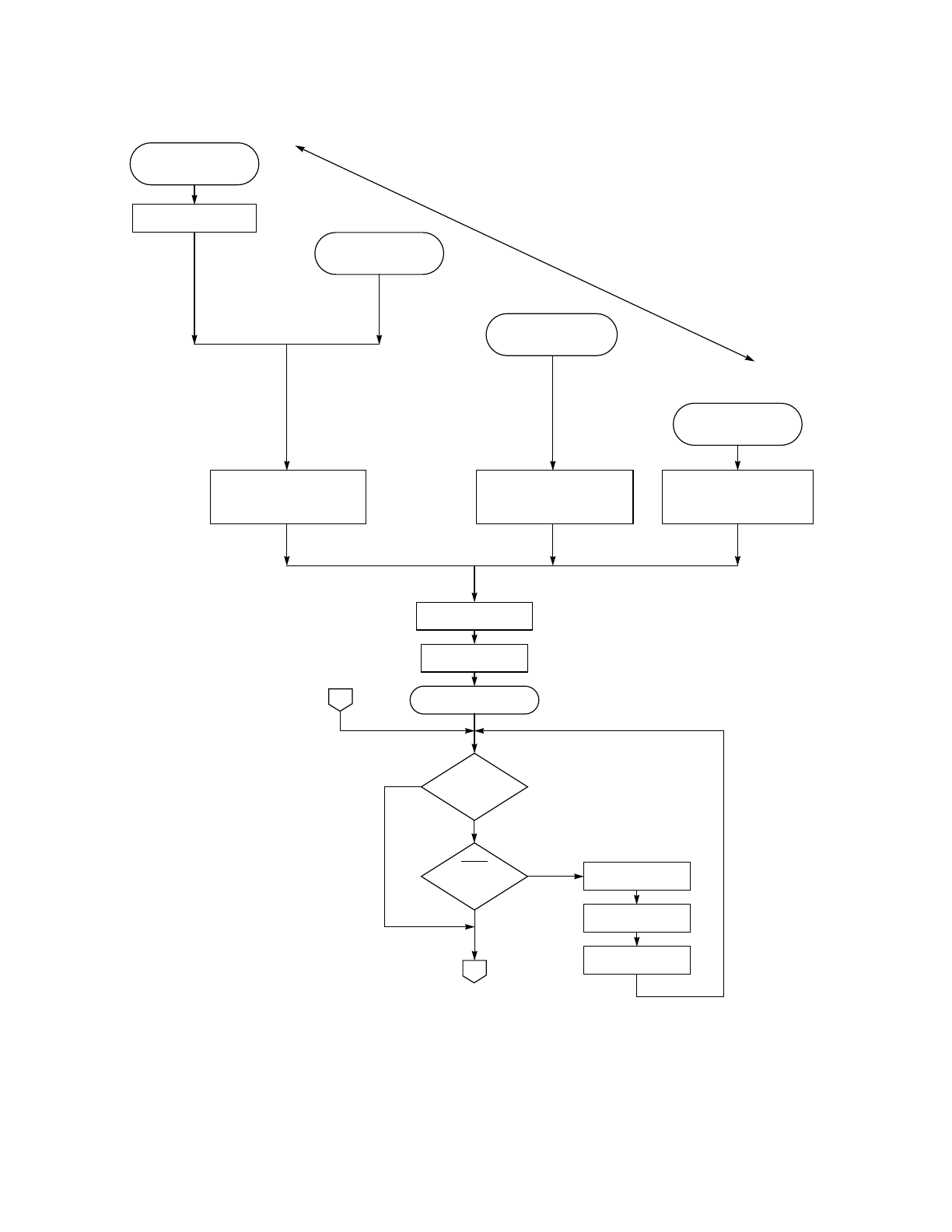
MOTOROLA RESETS AND INTERRUPTS M68HC11
5-16 REFERENCE MANUAL
Figure 5-2 Processing Flow out of Resets (Sheet 1 of 2)
1B
BIT X IN
Y
N
XIRQ Y
N
PIN LOW?
CCR = 1?
BEGIN INSTRUCTION
SEQUENCE
1A
STACK CPU
REGISTERS
SET BITS I AND X
FETCH VECTOR
$FFF4, $FFF5
SET BITS S,I, AND X
RESET MCU
HARDWARE
POWER-ON RESET
(POR)
EXTERNAL RESET
CLOCK MONITOR FAIL
(WITH CME = 1)
COP WATCHDOG
TIMEOUT
(WITH NOCOP = 0)
DELAY 4064 E CYCLES
LOAD PROGRAM COUNTER
WITH CONTENTS OF
$FFFE, $FFFF
(VECTOR FETCH)
LOAD PROGRAM COUNTER
WITH CONTENTS OF
$FFFC, $FFFD
(VECTOR FETCH)
LOAD PROGRAM COUNTER
WITH CONTENTS OF
$FFFA, $FFFB
(VECTOR FETCH)
HIGHEST
PRIORITY
LOWEST
PRIORITY
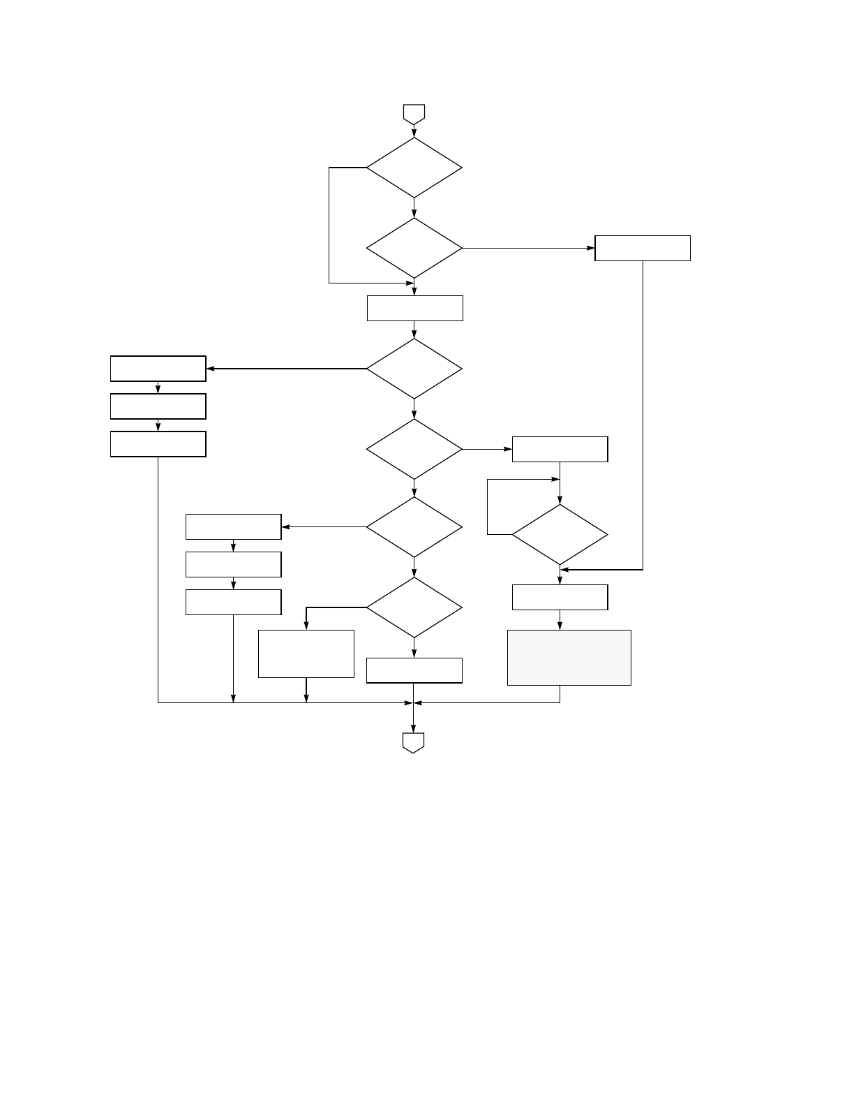
M68HC11 RESETS AND INTERRUPTS MOTOROLA
REFERENCE MANUAL 5-17
Figure 5-3 Processing Flow out of Resets (Sheet 2 of 2)
BIT I IN
CCR = 1?
1B
Y
N
ANY I-BIT
INTERRUPT Y
N
PENDING?
FETCH OPCODE
ILLEGAL
OPCODE?
Y
N
WAI Y
N
INSTRUCTION?
SWI
INSTRUCTION?
Y
N
RTI
INSTRUCTION?
Y
N
EXECUTE THIS
INSTRUCTION
STACK CPU
REGISTERS
ANY
N
Y
INTERRUPT
PENDING?
SET BIT I IN CCR
RESOLVE INTERRUPT
PRIORITY AND FETCH
VECTOR FOR HIGHEST
PENDING SOURCE
STACK CPU
REGISTERS
SET BIT I IN CCR
FETCH VECTOR
$FFF8, $FFF9
STACK CPU
REGISTERS
SET BIT I IN CCR
FETCH VECTOR
$FFF6, $FFF7
RESTORE CPU
REGISTERS
FROM STACK
1A
STACK CPU
REGISTERS
SEE FIGURE 5–3
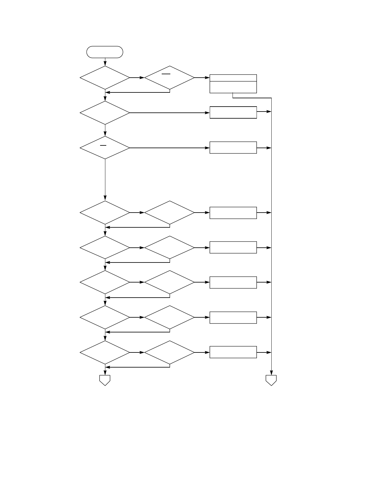
MOTOROLA RESETS AND INTERRUPTS M68HC11
5-18 REFERENCE MANUAL
Figure 5-4 Interrupt Priority Resolution (Sheet 1 of 2)
2A
BEGIN
SET X BIT IN CCR
FETCH VECTOR
$FFF4, FFF5
X BIT
IN CCR
SET ?
YES
NO
XIRQ PIN
LOW ?
YES
NO
HIGHEST
PRIORITY
INTERRUPT
?
YES
NO
IRQ ? YES
NO
FETCH VECTOR
$FFF2, FFF3
FETCH VECTOR
$FFF0, FFF1
RTII = 1 ? YES
NO
REAL-TIME
INTERRUPT
?
YES
NO
FETCH VECTOR
$FFEE, FFEF
IC1I = 1 ? YES
NO
TIMER
IC1F ?
YES
NO
FETCH VECTOR
$FFEC, FFED
IC2I = 1 ? YES
NO
TIMER
IC2F ?
YES
NO
FETCH VECTOR
$FFEA, FFEB
IC3I = 1 ? YES
NO
TIMER
IC3F ?
YES
NO
FETCH VECTOR
$FFE8, FFE9
OC1I = 1 ? YES
NO
TIMER
OC1F ?
YES
NO
2B
FETCH VECTOR
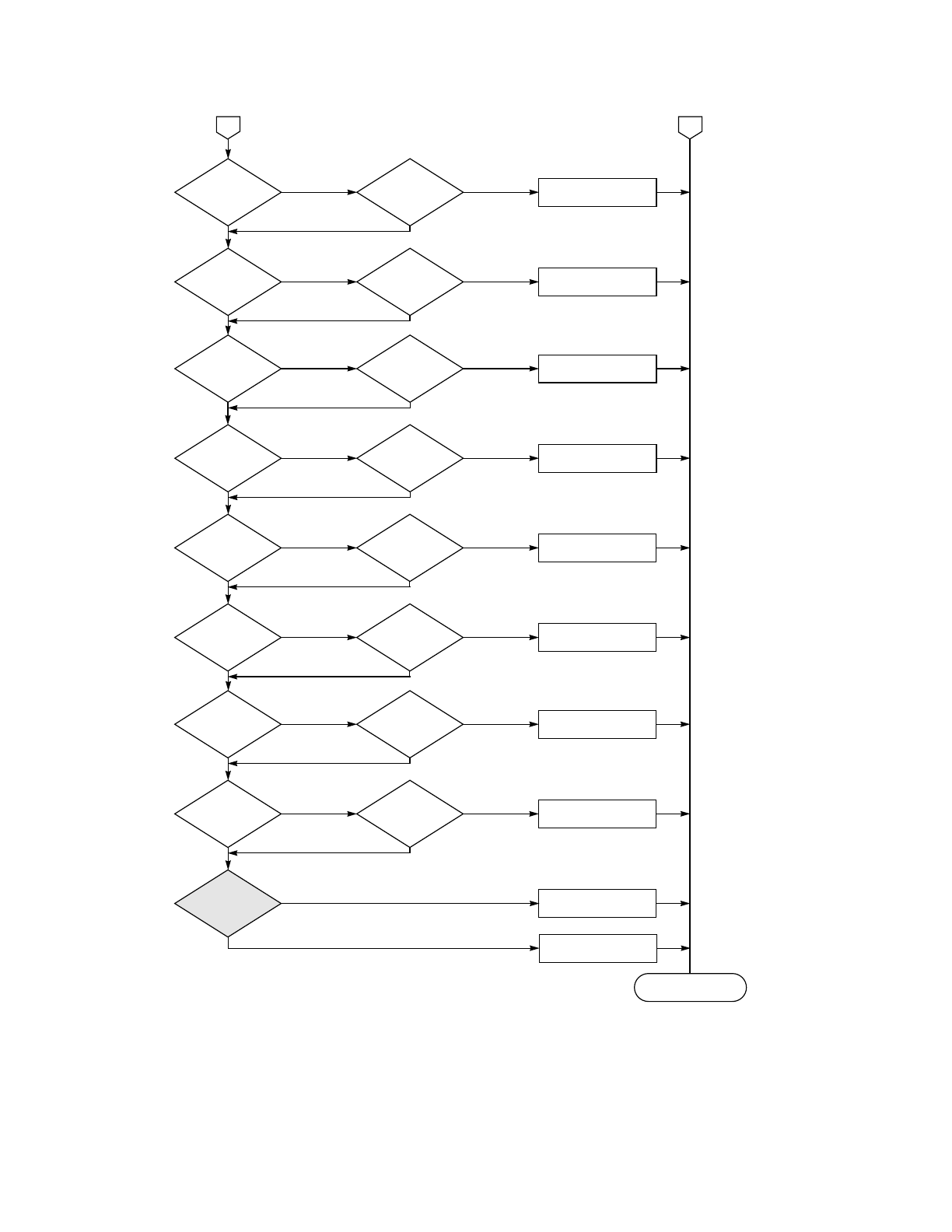
M68HC11 RESETS AND INTERRUPTS MOTOROLA
REFERENCE MANUAL 5-19
Figure 5-5 Interrupt Priority Resolution (Sheet 2 of 2)
TOI = 1? Y
N
Y
N
PAOVI = 1?
PAII = 1? Y
N
SPIE = 1? Y
N
Y
N
FLAG Y
N
Y
N
FLAG
FLAG Y
N
FLAGS Y
N
PAIF = 1?
SPIF = 1? OR
TOF = 1?
PAOVF = 1
FETCH VECTOR
$FFDE, $FFDF
FETCH VECTOR
$FFDC, $FFDD
FETCH VECTOR
$FFDA, $FFDB
FETCH VECTOR
$FFD6, $FFD7
FETCH VECTOR
$FFD8, $FFD9
OC2I = 1? Y
N
Y
N
OC3I = 1?
OC4I = 1? Y
N
OC5I = 1? Y
N
FLAG Y
N
Y
N
FLAG
FLAG Y
N
FLAG Y
N
OC4F = 1?
OC5F = 1?
OC2F = 1?
OC3F = 1
FETCH VECTOR
$FFE6, $FFE7
FETCH VECTOR
$FFE4, $FFE5
FETCH VECTOR
$FFE2, $FFE3
FETCH VECTOR
$FFE0, $FFE1
MODF = 1?
INTERRUPT?
SEE FIGURE
5-4
2A 2B
END
FETCH VECTOR
$FFF2, $FFF3
SCI
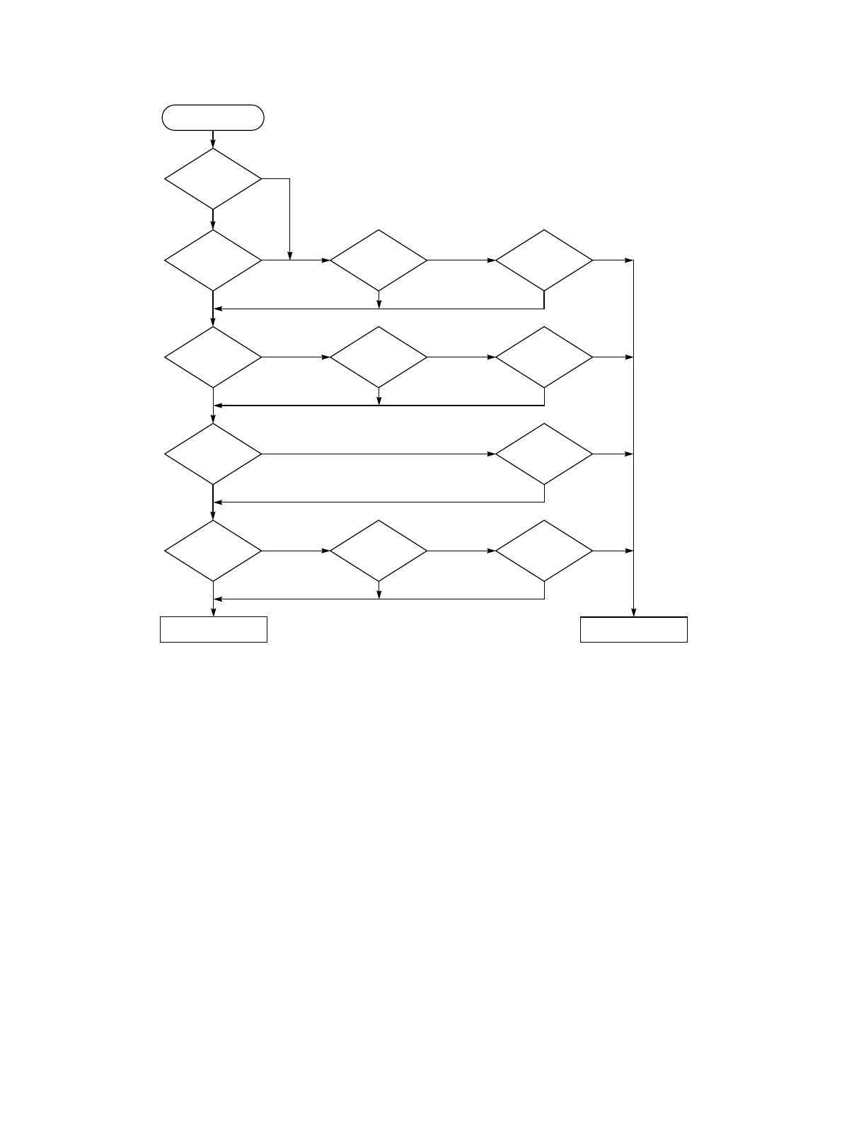
MOTOROLA RESETS AND INTERRUPTS M68HC11
5-20 REFERENCE MANUAL
Figure 5-6 Interrupt Source Resolution within SCI
5.3.3 Return from Interrupt
When an interrupt has been serviced as needed, the RTI instruction terminates inter-
rupt processing and returns to the program that was running at the time of the inter-
ruption. During servicing of the interrupt, some or all of the CPU registers will have
changed. To continue the former program as if it had not been interrupted, the regis-
ters must be restored to the values present at the time the former program was inter-
rupted. The RTI instruction accomplishes this by pulling (loading) the saved register
values from the stack memory. The last value to be pulled from the stack is the pro-
gram counter, which causes processing to resume where it was interrupted.
5.4 Non-Maskable Interrupts
This subsection discusses the illegal opcode fetch interrupt, the SWI instruction, and
FLAG Y
N
OR = 1? Y
N
Y
N
TDRE = 1?
TC = 1? Y
N
IDLE = 1? Y
N
Y
N
Y
N
Y
N
ILIE = 1?
RIE = 1?
TIE = 1?
BEGIN
RE = 1? Y
N
Y
N
TE = 1?
TCIE = 1? Y
N
RE = 1? Y
N
RDRF = 1?
VALID SCI REQUEST
NO
VALID SCI REQUEST

M68HC11 RESETS AND INTERRUPTS MOTOROLA
REFERENCE MANUAL 5-21
the XIRQ input pin. The illegal opcode fetch interrupt is a non-maskable interrupt
source intended to improve system integrity. Although it performs like an interrupt,
SWI is an instruction rather than an asynchronous interrupt. The XIRQ input is an up-
dated version of the non-maskable interrupt (NMI) input of earlier MCUs.
5.4.1 Non-Maskable Interrupt Request (XIRQ)
Non-maskable interrupts are useful because they can always interrupt CPU operation.
The most common use for such an interrupt is for very serious system problems, such
as program runaway or power failure. The XIRQ mechanism over-comes two signifi-
cant problems with an NMI input while retaining the important capabilities associated
with a non-maskable source.
The first NMI problem is as follows: What if an NMI is requested before the stack point-
er has been initialized? If this request happens, the register stacking operation causes
register values to be written to a random area of memory. If the stack pointer is point-
ing to some unimplemented memory area or to a read-only area, there will be no way
to return to the program in progress at the time of the interrupt. If the stack pointer is
pointing at a data area in memory, the register values will be written over the data (thus
corrupting it). Since this situation is not desirable, the NMI had to be externally inhibit-
ed after reset until the stack pointer could be initialized.
The second NMI problem is as follows: What if the NMI signal bounces so that NMI is
nested? If nesting occurs, the stack can be filled with several copies of the register val-
ues, possibly filling the stack beyond its allotted space. Nesting in this way would also
cause excessive latency from the request until the resulting program actions are exe-
cuted.
The M68HC11 solves both these problems with the X bit in the CCR. The X bit is very
similar to the I bit except that there are special restrictions on setting and clearing of
the X bit. Since X can only be cleared by a software instruction, the programmer has
control over when the XIRQ input becomes enabled. The two software instructions
that can clear the X bit are TAP and RTI (provided the stacked CCR value has a zero
in the X bit position). The two hardware conditions that can set the X bit are system
reset and the recognition of an XIRQ.
Immediately after any reset, the X bit is set; thus, XIRQ is inhibited. When software
has established initial conditions, including setting the stack pointer, the X bit may be
cleared with a TAP instruction to enable XIRQ. These two steps overcome the first
NMI problem. Since software cannot set the X bit, the XIRQ can be considered a non-
maskable source at this point. When an XIRQ occurs, the CCR value is stacked (with
the X bit clear); the X bit is then automatically set to inhibit additional interrupts. This
step overcomes the second NMI problem. When an RTI instruction is executed, the
CCR is restored to the stacked value (which had the X bit clear). A common miscon-
ception is that the X bit can be set by executing an RTI instruction with a one in the X
bit position of the stacked CCR value. In reality, the X bit is implemented as a set-reset
flip-flop rather than a D-type flip-flop. The set input is connected to the OR of reset and
XIRQ acknowledge. The reset input is connected to the AND of a CCR write and data
bit 6 equals zero. If an attempt is made to TAP or unstack a one to the X bit, neither

MOTOROLA RESETS AND INTERRUPTS M68HC11
5-22 REFERENCE MANUAL
the set nor the clear input to the X bit flip-flop will be activated, and the X bit will remain
unchanged.
The M68HC11 supports a STOP mode where all clocks are stopped to reduce power
consumption to a few microamps. Recovery to active mode is accomplished by a reset
or an interrupt (IRQ or XIRQ). Depending upon the state of the X bit in the CCR, the
XIRQ input offers a choice of two recovery methods. If X is zero, XIRQ interrupts are
enabled, and recovery leads to register stacking and normal interrupt service. If X is
one, XIRQ interrupts are inhibited, but the XIRQ pin can still be used for recovery from
the STOP mode. Rather than resuming operation with service of an interrupt (XIRQ),
the clocks start and processing resumes with the next opcode after the STOP opcode.
This technique can be thought of as a STOP-continue mechanism.
Some M68HC11 MCUs were manufactured with a subtle defect that can cause failure
to properly recover from STOP with an interrupt input (IRQ or XIRQ). If the opcode im-
mediately preceding the STOP opcode came from column 4 or 5 of the opcode map,
recovery was incorrect. Column 4 and 5 opcodes are accumulator instructions, such
as negate A (NEGA) or decrement B (DECB), which seldom appear immediately be-
fore a STOP instruction; therefore, a long time elapsed before the problem was dis-
covered. A simple NOP instruction before the STOP opcode assures proper recovery
from STOP in all cases.
5.4.2 Illegal Opcode Fetch
Since not all possible opcodes or opcode sequences are defined, an illegal opcode de-
tection circuit has been included. When an illegal opcode is detected, an interrupt is
requested to the illegal opcode vector. The illegal opcode vector should never be left
uninitialized. The stack pointer should be re-initialized as a result of an illegal opcode
interrupt so repeated execution of illegal opcodes does not cause stack overruns. If
the illegal opcode vector were left uninitialized, it could point to a memory location that
contained an illegal opcode. In such a case, there would be an infinite loop of repeated
illegal opcodes and an infinite stack overflow, which would cause the register contents
to be stored to all memory addresses in a very short time.
The illegal opcode trap mechanism works for all unimplemented opcodes on all four
opcode-map pages. The address stacked as the return address for the illegal opcode
interrupt is the address of the first byte of the illegal opcode. Otherwise, it would be
almost impossible to determine whether the illegal opcode had been one or two bytes.
The stacked return address can be used as a pointer to the illegal opcode so the illegal
opcode service routine can evaluate the offending opcode.
The illegal opcode mechanism can be used to create a number of special-purpose in-
structions that use otherwise illegal opcodes. When one of these opcodes is encoun-
tered, the interrupt service routine can look up the special opcocde and perform some
special task. The return address would need to be manually changed since it points to
the illegal opcode rather than to the instruction that follows the illegal opcode.
The TEST Instruction (opcode $00) is a legal opcode in special test and bootstrap
modes, but it is an especially offensive illegal opcode in normal operating modes. The

M68HC11 RESETS AND INTERRUPTS MOTOROLA
REFERENCE MANUAL 5-23
illegal opcode detection logic treats the TEST opcode as illegal when the MCU is in
normal operating modes and as legal in special test and bootstrap modes.
5.4.3 Software Interrupt
The SWI is executed in the same manner as other instructions and takes precedence
over pending interrupts only if the other interrupts are masked (I and X bits in the CCR
set). The SWI instruction is executed in a manner similar to other maskable interrupts
in that it sets the I bit, CPU registers are stacked, etc. SWI is not inhibited by the global
interrupt mask bits (X or I) in the CCR.
NOTE
The SWI instruction will not be fetched if any other interrupt is pend-
ing. However, once an SWI instruction begins, no other interrupt can
be honored until the SWI vector has been fetched.
SWI instructions are commonly used in debug monitors to transfer control from a user
program to the debug monitor. For example, while operating under monitor control, a
designer can specify a breakpoint at some address in the user program being de-
bugged. The monitor will replace the user’s opcode at this address with the opcode for
an SWI instruction. When the user’s program is running and this SWI opcode is en-
countered, the monitor, recognizing that this is a breakpoint, will take control. The SWI
opcodes are usually placed into the user’s program just before the program is run, and
these locations are restored to the original opcode when the debug monitor regains
control.
5.5 Maskable Interrupts
The remaining twenty interrupt sources in the MC68HC11A8 are subject to masking
by a global interrupt mask bit (I bit in CCR). In addition to the global I bit, all of these
sources except the external interrupt (IRQ pin) are subject to local enable bits in con-
trol registers. Most interrupt sources in the M68HC11 have separate interrupt vectors;
thus, there is usually no need for software to poll control registers to determine the
cause of an interrupt. The maskable interrupt sources respond to a fixed-priority rela-
tionship except that any one source can be dynamically elevated to the highest priority
position of any maskable source.
This subsection discusses the maskable interrupt structure rather than the specific in-
terrupts from individual internal peripheral subsystems. The interrupts associated with
the internal subsystems are discussed throughout this manual during the discussion
of each peripheral system.
5.5.1 I Bit in the Condition Code Register
The I bit in the CCR acts as a primary enable control for all maskable interrupts. When
the I bit is set, interrupts can become pending but will not be honored. When the I bit
is clear, interrupts are enabled to interrupt normal program flow when an interrupt
source requests service.
The I bit is set during reset to prevent interrupts from being honored until minimum sys-

MOTOROLA RESETS AND INTERRUPTS M68HC11
5-24 REFERENCE MANUAL
tem initialization has been performed. Part of this minimum initialization would be to
load the stack pointer so it points to an appropriate area of RAM. The I bit is also au-
tomatically set during entry into any interrupt service routine to prevent an infinite
source of interrupts from overwhelming the CPU. Software can also set the interrupt
mask bit to inhibit interrupts during sensitive operations.
The I bit can be cleared by software instructions or during the execution of an RTI in-
struction. In most applications, the I bit remains set during interrupt service routines so
other interrupts will not be honored until a current interrupt service routine finishes (i.e.,
nesting is not permitted). In more unusual applications, it is possible to allow nesting
of interrupts by clearing the I bit during an interrupt service routine. Since this proce-
dure requires much expertise, it should not be attempted by a novice programmer. In
some cases, worst-case interrupt latency can be reduced by allowing interrupt nesting,
but usually the best procedure is to minimize the execution time of interrupt service
routines. Since the overhead associated with interrupt nesting usually violates this pro-
cedure, nesting is not recommended.
The operation of the I bit during service of an interrupt proceeds as follows. When an
enabled interrupt occurs and the I bit is clear, the CPU completes the current instruc-
tion and begins the interrupt response sequence. The current contents of the CPU reg-
isters are pushed onto the stack (stored in stack RAM). The register values are saved
one byte at a time in the following order: PCL, PCH, IYL, IYH, IXL, IXH, ACCA, ACCB,
and CCR. After the CCR value is stacked, the I bit in the CCR is set to inhibit further
interrupts. Next, the vector for the highest priority pending interrupt is fetched, and pro-
cessing continues with execution of the first instruction in the interrupt service routine.
The last instruction in the interrupt service routine is the RTI instruction. This instruc-
tion causes the previously stacked register values to be loaded back into the registers
in reverse order. Since the program counter is restored to its pre-interrupt value, the
next instruction executed will be the instruction that would have been executed if the
interrupt had not occurred.
A common error for new users is to put a set interrupt mask (SEI) instruction at the
beginning of an interrupt service routine and a clear interrupt mask (CLI) instruction
just before the RTI instruction. These instructions should not be used in this way be-
cause they are redundant. The automatic interrupt logic already sets the I bit on the
way into an interrupt and clears the I bit during normal execution of the RTI instruction.
5.5.2 Special Considerations for I-Bit-Related Instructions
There are some special conditions associated with the I bit that require additional con-
sideration. The I bit is actually a sequential logic circuit rather than a simple flip-flop.
When the I bit is set by an SEI or a TAP instruction, interrupts are inhibited immediate-
ly. An interrupt occurring while an SEI instruction is executing will not be honored until
unless the I bit is later cleared. When the I bit is cleared by a CLI or TAP instruction,
the actual clear operation is delayed for one bus cycle so the instruction following the
CLI or TAP will always be executed. This procedure implies that the following loop can
never be interrupted by a maskable interrupt:

M68HC11 RESETS AND INTERRUPTS MOTOROLA
REFERENCE MANUAL 5-25
The reason for this delayed clear operation can be seen in the next instruction se-
quence:
If there were not a delay in clearing the I bit, it is possible the interrupt could be recog-
nized between the CLI and WAI instructions. Upon return from the interrupt service
routine, the WAI instruction would be executed, and the CPU would erroneously wait
for the interrupt that was just serviced.
During execution of an RTI instruction, the first register to be restored from the stack
is the CCR. In this situation, the one-cycle delay in clearing the I bit expires long before
the RTI instruction is finished; thus, a new interrupt sequence can be started even be-
fore a single instruction of the interrupted program is executed.
5.6 Interrupt Request
The maskable interrupt structure in the M68HC11 can be extended to additional exter-
nal interrupting sources through the IRQ input. This subsection discusses the IRQ in-
put as it relates to the interrupt structure. The alternate use of the IRQ pin as an
EEPROM programming voltage source during factory testing is discussed in 2.2.6 In-
terrupt Pins (XIRQ, IRQ).
Although this subsection is primarily concerned with the IRQ pin, there are several ad-
ditional MCU pins that can be used as interrupt inputs. The XIRQ pin provides for non-
maskable interrupts. The main-timer input-capture pins (IC[3:1]) can be used as edge-
sensitive interrupt inputs with separate controls for selecting the significant edge and
separate interrupt vectors. The pulse accumulator input pin can also be used as an
additional edge-sensitive interrupt. If the MCU is operating in single-chip mode, the
strobe A (STRA/AS) pin is available as an edge-triggered interrupt input. Though there
is only one IRQ pin, these other pins allow an MC68HC11A8 to have up to seven in-
terrupt pins.
5.6.1 Selecting Edge Triggering or Level Triggering
The default (most common) configuration for the IRQ pin in an M68HC11 application
is a low-level-sensitive wired-OR network. In less common applications, IRQ can be a
low-going edge-sensitive input. The edge-sensitive configuration is less common be-
cause it only allows a single interrupt source to use the IRQ pin; whereas, the level-
sensitive configuration can accommodate many sources on the single IRQ pin. The
IRQ select edge-sensitive only IRQE bit in the OPTION control register is used to se-
lect the IRQ pin configuration (IRQE = 0 for low level sensitive and IRQE = 1 for low-
going edge sensitive). The IRQE control bit is time-protected, which means it can only
LOOP CLI Enable Interrupts
SEI Disable Interrupts
BRA LOOP Repeat
CLI Enable Interrupts
WAI Wait for an Interrupt

MOTOROLA RESETS AND INTERRUPTS M68HC11
5-26 REFERENCE MANUAL
be written once within the first 64 E-clock cycles after reset. IRQE is cleared by default
during reset.
The interrupt sources within the MCU all operate as a wired-OR level-sensitive net-
work. When an event triggers an interrupt, a software-accessible interrupt flag is set,
which (if enabled) causes a constant request for interrupt service. When software has
recognized the interrupt, this flag is cleared, thus releasing the request for service. The
flag bit acts as a static indication that service is required. If more than one interrupt
source is connected to a single level-sensitive line, the line may remain asserted for
several overlapping events from different sources, and the flag bits assure that all re-
quests will be serviced.
In an edge-sensitive network, the MCU is responsible for latching a request upon rec-
ognition of a low-going edge at the interrupt input. This configuration is only capable
of recognizing that an edge occurred (there is no software-accessible record to identify
the requesting source); thus, the edge-sensitive configuration is appropriate only
where a single source could have made the request.
5.6.2 Sharing Vector with Handshake I/O Interrupts
Because the IRQ vector is shared by the handshake I/O subsystem and the IRQ input
pin, the handshake I/O functions can be rebuilt externally when the MCU is operating
in expanded modes. While the MCU is in an expanded mode, 18 pins, which were
used for the handshake I/O subsystem, become dedicated to the expansion bus. The
MC68HC24 is a port replacement unit (PRU) that rebuilds the handshake I/O func-
tions. The MCU is specifically designed to treat the associated addresses as external
locations while in expanded modes so that software sees no difference between an
expanded system with a PRU and an M68HC11 operating in single-chip mode. Since
the handshake I/O system uses the same vector as the IRQ pin, the PRU can drive
the IRQ pin of the MCU. Even the interrupts for the handshake I/O system are faithfully
emulated.
The shared interrupt with IRQ solves most emulation problems for the PRU; however,
there are some difficulties in applications where IRQ is configured for edge-sensitive
operation. In such a system, the PRU is connected to the IRQ pin and to the user’s
external interrupt source. The edge-sensitive configuration is not able to distinguish
which source caused an interrupt. Also, if an edge-triggered interrupt is generated by
the external source while an interrupt is pending from the PRU, the low level on the
IRQ line prevents any new-edge from being detected. Since the level-sensitive config-
uration is more common for IRQ and since so many other pins can act as edge-sensi-
tive interrupt inputs, this limitation should not be serious.
5.7 Interrupts from Internal Peripheral Subsystems
The following paragraphs discuss common aspects of the interrupts generated by on-
chip peripheral systems. The interrupt sources for on-chip peripheral systems are dis-
cussed in greater detail in the sections for each peripheral system.

M68HC11 RESETS AND INTERRUPTS MOTOROLA
REFERENCE MANUAL 5-27
5.7.1 Inhibiting Individual Sources
All on-chip interrupt sources have software-accessible control bits to enable the inter-
rupt sources on an individual basis. Each source has a flag bit, which indicates service
is required, and an interrupt enable bit, which enables the flag to generate hardware
interrupt requests. The programmer decides which sources will be used to generate
interrupts and which will be handled by software polling rather than by interrupts. The
global interrupt mask (I bit in CCR) can be used to inhibit all maskable interrupts.
5.7.2 Clearing Interrupt Status Flag Bits
The method for clearing the interrupt status flags varies from one system to another.
Detailed explanations of the clearing requirements for each flag are provided in the
sections for each on-chip peripheral system.
Timer system interrupt flags are cleared by writing a logic one to the flag bit positions
to be cleared. This action is explicit and is intended to prevent these flags from being
cleared unintentionally. The most straightforward way to accomplish clearing is to load
an accumulator with an immediate value (with ones in the bit positions corresponding
to a flag bit(s) to be cleared) and then write this value to the status register. Other in-
struction sequences can be used to clear these timer flag bits, including bit manipula-
tion instructions. Several instruction sequences for clearing timer flags are discussed
in detail in 10.2.4 Tips for Clearing Timer Flags.
5.7.3 Automatic Clearing Mechanisms on Some Flags
For some of the interrupt sources, such as the parallel I/O interrupt and the SCI inter-
rupts, the flags are automatically cleared during the normal course of responding to
the interrupt requests. For example, the RDRF flag in the SCI system is cleared by the
automatic clearing mechanism consisting of a read of the SCI status register while
RDRF is set, followed by a read of the SCI data register. The normal response to an
RDRF interrupt request would be to read the SCI status register to check for receive
errors, then read the received data from the SCI data register. These two steps satisfy
the automatic clearing mechanism without requiring any special instructions.
In unusual cases, a programmer must take special care not to unintentionally trigger
the automatic clearing mechanisms. The following guidelines help to avoid such prob-
lems. Reads of registers containing status flags should be minimized. Ideally, the sta-
tus register should be read only during the course of servicing the interrupt, and the
status flag should be read only once for each time the interrupt is requested. If more
than one part of the service routine uses different bits in the status register, the register
should be read only once, and a copy should be kept in RAM or in a CPU register for
further use. The cycle-by-cycle operation of instructions that access status registers
may also present another problem. Some instructions are read-modify-write instruc-
tions even though the read information is not actually needed for the instruction. For
example, the clear (CLR) instruction performs a read of the operand address even
though the value read is irrelevant. A situation could arise where the SCI data register
is cleared to transmit a $00 value via the SCI transmitter. Though it is not obvious, this
action can satisfy the second step of the automatic clearing mechanism for the RDRF
flag because clearing of the SCI transmit data register involves a read of the SCI data

MOTOROLA RESETS AND INTERRUPTS M68HC11
5-28 REFERENCE MANUAL
register prior to the write of $00.

M68HC11 CENTRAL PROCESSING UNIT MOTOROLA
REFERENCE MANUAL 6-1
SECTION 6
CENTRAL PROCESSING UNIT
This section discusses the M68HC11 central processing unit (CPU), which is respon-
sible for executing all software instructions in their programmed sequence. The
M68HC11 CPU can execute all M6800 and M6801 instructions (source and object-
code compatible) and more than 90 new instruction opcodes. Since more than 256 in-
struction opcodes exist, a multiple-page opcode map is used in which some new in-
structions are specified by a page-select prebyte before the opcode byte.
The architecture of the M68HC11 CPU causes all peripheral, I/O, and memory loca-
tions to be treated identically as locations in the 64-Kbyte memory map. Thus, there
are no special instructions for I/O that are separate from those used for memory. This
technique is sometimes called "memory-mapped I/O". In addition, there is no execu-
tion-time penalty for accessing an operand from an external memory location as op-
posed to a location within the MCU.
The M68HC11 CPU offers several new capabilities when compared to the earlier
M6801 and M6800 CPUs. The biggest change is the addition of a second 16-bit index
register (Y). Powerful, new bit-manipulation instructions are now included, allowing
manipulation of any bit or combination of bits in any memory location in the 64-Kbyte
address space. Two new 16-bit by 16-bit divide instructions are included. Exchange
instructions allow the contents of either index register to be exchanged with the con-
tents of the 16-bit double accumulator. Finally, several instructions have been upgrad-
ed to make full 16-bit arithmetic operations even easier than before.
This section discusses the CPU architecture, addressing modes, and the instruction
set (by instruction types). Examples are included to show efficient ways of using this
architecture and instruction set. To condense this section, detailed explanations of
each instruction are included in APPENDIX A INSTRUCTION SET DETAILS. These
explanations include detailed cycle-by-cycle bus activity and boolean expressions for
condition code bits. This section should be used to gain a general understanding of
the CPU and instruction set.
6.1 Programmer’s Model
Figure 6-1 shows the programmer’s model of the M68HC11 CPU. The CPU registers
are an integral part of the CPU and are not addressed as if they were memory loca-
tions. Each of these registers is discussed in the subsequent paragraphs.
6.1.1 Accumulators (A, B, and D)
Accumulators A and B are general-purpose 8-bit accumulators used to hold operands
and results of arithmetic calculations or data manipulations. Some instructions treat
the combination of these two 8-bit accumulators as a 16-bit double accumulator (ac-
cumulator D).

MOTOROLA CENTRAL PROCESSING UNIT M68HC11
6-2 REFERENCE MANUAL
Figure 6-1 M68HC11 Programmer’s Model
Most operations can use accumulator A or B interchangeably; however, there are a
few notable exceptions. The ABX and ABY instructions add the contents of the 8-bit
accumulator B to the contents of the 16-bit index register X or Y, and there are no
equivalent instructions that use A instead of B. The TAP and TPA instructions are used
to transfer data from accumulator A to the condition code register or from the condition
code register to accumulator A; however, there are no equivalent instructions that use
B rather than A. The decimal adjust accumulator A (DAA) instruction is used after bi-
nary-coded decimal (BCD) arithmetic operations, and there is no equivalent BCD in-
struction to adjust B. Finally, the add, subtract, and compare instructions involving
both A and B (ABA, SBA, and CBA) only operate in one direction; therefore, it is im-
portant to plan ahead so the correct operand will be in the correct accumulator.
6.1.2 Index Registers (X and Y)
The 16-bit index registers X and Y are used for indexed addressing mode. In the in-
dexed addressing mode, the contents of a 16-bit index register are added to an 8-bit
offset, which is included as part of the instruction, to form the effective address of the
operand to be used in the instruction. In most cases, instructions involving index reg-
ister Y take one extra byte of object code and one extra cycle of execution time com-
pared to the equivalent instruction using index register X. The second index register is
especially useful for moves and in cases where operands from two separate tables are
involved in a calculation. In the earlier M6800 and M6801, the programmer had to
store the index to some temporary location so the second index value could be loaded
into the index register.
8-BIT ACCUMULATORS A & B
7070
15 0
AB
D
IX
IY
SP
PC
70
CVZNIHXS
OR 16-BIT DOUBLE ACCUMULATOR D
INDEX REGISTER X
INDEX REGISTER Y
STACK POINTER
PROGRAM COUNTER
CARRY/BORROW FROM MSB
OVERFLOW
ZERO
NEGATIVE
I-INTERRUPT MASK
HALF CARRY (FROM BIT 3)
X-INTERRUPT MASK
STOP DISABLE
CONDITION CODES

M68HC11 CENTRAL PROCESSING UNIT MOTOROLA
REFERENCE MANUAL 6-3
The ABX and ABY instructions along with increment and decrement instructions allow
some arithmetic operations on the index registers, but, in some cases, more powerful
calculations are needed. The exchange instructions, XGDX and XGDY, offer a very
simple way to load an index value into the 16-bit double accumulator, which has more
powerful arithmetic capabilities than the index registers themselves.
It is very common to load one of the index registers with the beginning address of the
internal register space (usually $1000), which allows the indexed addressing mode to
be used to access any of the internal I/O and control registers. Indexed addressing re-
quires fewer bytes of object code than the corresponding instruction using extended
addressing. Perhaps a more important argument for using indexed addressing to ac-
cess register space is that bit-manipulation instructions are available for indexed ad-
dressing but not for extended addressing.
6.1.3 Stack Pointer (SP)
The M68HC11 CPU automatically supports a program stack. This stack may be locat-
ed anywhere in the 64-Kbyte address space and may be any size up to the amount of
memory available in the system. Normally, the stack pointer register is initialized by
one of the very first instructions in an application program. Each time a byte is pushed
onto the stack, the stack pointer is automatically decremented, and each time a byte
is pulled off the stack, the stack pointer is automatically incremented. At any given
time, the stack pointer register holds the 16-bit address of the next free location on the
stack. The stack is used for subroutine calls, interrupts, and for temporary storage of
data values.
When a subroutine is called by a jump to subroutine (JSR) or branch to subroutine
(BSR) instruction, the address of the next instruction after the JSR or BSR is automat-
ically pushed onto the stack (low half first). When the subroutine is finished, a return
from subroutine (RTS) instruction is executed. The RTS causes the previously stacked
return address to be pulled off the stack, and execution continues at this recovered re-
turn address.
Whenever an interrupt occurs (provided it is not masked), the current instruction fin-
ishes normally, the address of the next instruction (the current value in the program
counter) is pushed onto the stack, all of the CPU registers are pushed onto the stack,
and execution continues at the address specified by the vector for the highest priority
pending interrupt. After completing the interrupt service routine, a return from interrupt
(RTI) instruction is executed. The RTI instruction causes the saved registers to be
pulled off the stack in reverse order, and program execution resumes as if there had
been no interruption.
Another common use for the stack is for temporary storage of register values. A simple
example would be a subroutine using accumulator A. The user could push accumula-
tor A onto the stack when entering the subroutine and pull it off the stack just before
leaving the subroutine. This method is a simple way to assure a register(s) will be the
same after returning from the subroutine as it was before starting the subroutine.
The most important aspect of the stack is that it is completely automatic. A program-

MOTOROLA CENTRAL PROCESSING UNIT M68HC11
6-4 REFERENCE MANUAL
mer does not normally have to be concerned about the stack other than to be sure that
it is pointing at usable random-access memory (RAM) and that there is sufficient
space. To assure sufficient space, the user would need to know the maximum depth
of subroutine or interrupt nesting possible in the particular application.
There are a few less common uses for the stack. The stack can be used to pass pa-
rameters to a subprogram, which is fairly common in high-level language compilers
but is often overlooked by assembly-language programmers. There are two advantag-
es of this technique over specific assignment of temporary or variable locations. First,
the memory locations are only needed for the time the subprogram is being executed;
they can be used for something else when the subprogram is completed. Second, this
feature makes the subprogram re-entrant so that an interrupting program could call the
same subprogram with a different set of values without disturbing the interrupted use
of the subprogram.
In unusual cases, a programmer may want to look at or even manipulate something
that is on the stack, which should only be attempted by an experienced programmer
because it requires a detailed understanding of how the stack operates. Monitor pro-
grams like BUFFALO sometimes place items on a stack manually and then perform
an RTI instruction to go to a user program. This technique is an odd use of the stack
and RTI instruction because an RTI would normally correspond to a previous interrupt.
6.1.4 Program Counter (PC)
The program counter is a 16-bit register that holds the address of the next instruction
to be executed.
6.1.5 Condition Code Register (CCR)
This register contains five status indicators, two interrupt masking bits, and a STOP
disable bit. The register is named for the five status bits since that is the major use of
the register. In the earlier M6800 and M6801 CPUs, there was no X interrupt mask and
no STOP disable control in this register.
The five status flags reflect the results of arithmetic and other operations of the CPU
as it performs instructions. The five flags are half carry (H), negative (N), zero (Z),
overflow (V), and carry/borrow (C). The half-carry flag, which is used only for BCD
arithmetic operations (see 6.3.1.2 Arithmetic Operations), is only affected by the add
accumulators A and B (ABA), ADD, and add with carry (ADC) addition instructions (21
opcodes total). The N, Z, V, and C status bits allow for branching based on the results
of a previous operation. Simple branches are included for either state of any of these
four bits. Both signed and unsigned versions of branches are provided for the condi-
tions <, ≤, =, ≠,≥, or >.
The H bit indicates a carry from bit 3 during an addition operation. This status indicator
allows the CPU to adjust the result of an 8-bit BCD addition so it is in correct BCD for-
mat, even though the add was a binary operation. This H bit, which is only updated by
the ABA, ADD, and ADC instructions, is used by the DAA instruction to compensate
the result in accumulator A to correct BCD format.

M68HC11 CENTRAL PROCESSING UNIT MOTOROLA
REFERENCE MANUAL 6-5
The N bit reflects the state of the most significant bit (MSB) of a result. For two’s com-
plement, a number is negative when the MSB is set and positive when the MSB is ze-
ro. The N bit has uses other than in two’s-complement operations. By assigning an
often tested flag bit to the MSB of a register or memory location, the user can test this
bit by loading an accumulator.
The Z bit is set when all bits of the result are zeros. Compare instructions do an internal
implied subtraction, and the condition codes, including Z, reflect the results of that sub-
traction. A few operations (INX, DEX, INY, and DEY) affect the Z bit and no other con-
dition flags. For these operations, the user can only determine = and ≠.
The V bit is used to indicate if a two’s-complement overflow has occurred as a result
of the operation.
The C bit is normally used to indicate if a carry from an addition or a borrow has oc-
curred as a result of a subtraction. The C bit also acts as an error flag for multiply and
divide operations. Shift and rotate instructions operate with and through the carry bit
to facilitate multiple-word shift operations.
In the M68HC11 CPU, condition codes are automatically updated by almost all instruc-
tions; thus, it is rare to execute any extra instructions to specifically update the condi-
tion codes. For example, the load accumulator A (LDAA) and store accumulator A
(STAA) instructions automatically set or clear the N, Z, and V condition code flags. (In
some other architectures, very few instructions affect the condition code bits; thus, it
takes two instructions to load and test a variable.) The challenge in a Motorola proces-
sor lies in finding instructions that specifically do not alter the condition codes in rare
cases where that is desirable. The most important instructions that do not alter condi-
tions codes are the pushes, pulls, add B to X (ABX), add B to Y (ABY), and 16-bit trans-
fers and exchanges. It is always a good idea to refer to an instruction set summary
such as the pocket guide (MC68HC11A8RG/AD) to check which condition codes are
affected by a particular instruction.
The STOP disable (S) bit is used to allow or disallow the STOP instruction. Some us-
ers consider the STOP instruction dangerous because it causes the oscillator to stop;
however, the user can set the S bit in the CCR to disallow the STOP instruction. If the
STOP instruction is encountered by the CPU while the S bit is set, it will be treated like
a no-operation (NOP) instruction, and processing continues to the next instruction.
The interrupt request (IRQ) mask (I bit) is a global mask that disables all maskable in-
terrupt sources. While the I bit is set, interrupts can become pending and are remem-
bered, but CPU operation continues uninterrupted until the I bit is cleared. After any
reset, the I bit is set by default and can only be cleared by a software instruction. When
any interrupt occurs, the I bit is automatically set after the registers are stacked but be-
fore the interrupt vector is fetched. After the interrupt has been serviced, an RTI in-
struction is normally executed, restoring the registers to the values that were present
before the interrupt occurred. Normally, the I bit would be zero after an RTI was exe-
cuted. Although interrupts can be re-enabled within an interrupt service routine, to do
so is unusual because nesting of interrupts becomes possible, which requires much
more programming care than single-level interrupts and seldom improves system per-

MOTOROLA CENTRAL PROCESSING UNIT M68HC11
6-6 REFERENCE MANUAL
formance.
The XIRQ mask (X bit) is used to disable interrupts from the XIRQ pin. After any reset,
X is set by default and can only be cleared by a software instruction. When XIRQ is
recognized, the X bit (and I bit) are automatically set after the registers are stacked but
before the interrupt vector is fetched. After the interrupt has been serviced, an RTI in-
struction is normally executed, causing the registers to be restored to the values that
were present before the interrupt occurred. It is logical to assume the X bit was clear
before the interrupt; thus, the X bit would be zero after the RTI was executed. Although
XIRQ can be re-enabled within an interrupt service routine, to do so is unusual be-
cause nesting of interrupts becomes possible, which requires much more program-
ming care than single-level interrupts.
6.2 Addressing Modes
In the M68HC11 CPU, six addressing modes can be used to reference memory: im-
mediate, direct, extended, indexed (with either of two 16-bit index registers and an 8-
bit offset), inherent, and relative. Some instructions require an additional byte (a pre-
byte) before the opcode to accommodate a multiple-page opcode map.
Each of the addressing modes (except inherent) results in an internally generated,
double-byte value referred to as the effective address. This value, which is the result
of a statement operand field, is the value that appears on the address bus during the
memory reference portion of the instruction. The addressing mode is an implicit part
of every M68HC11 instruction.
Bit-manipulation instructions actually employ two or three addressing modes during
execution but are classified by the addressing mode used to access the primary oper-
and. All bit-manipulation instructions use immediate addressing to fetch a bit mask,
and branch variations use relative addressing mode to determine a branch destina-
tion.
The following paragraphs provide a description of each addressing mode. In these de-
scriptions, effective address is used to indicate the memory address from which the
argument is fetched or stored or from which execution is to proceed.
6.2.1 Immediate (IMM)
In the immediate addressing mode, the actual argument is contained in the byte(s) im-
mediately following the instruction in which the number of bytes matches the size of
the register. These instructions are two, three, or four (if prebyte is required) bytes.
Machine-code byte(s) that follow the opcode are the value of the statement rather than
the address of a value. In this case, the effective address of the instruction is specified
by the character # sign and implicitly points to the byte following the opcode. The im-
mediate value is limited to either one or two bytes, depending on the size of the regis-
ter involved in the instruction. Examples of several assembly-language statements
using the immediate addressing mode are shown. Symbols and expression used in
these statements are defined immediately after the examples.

M68HC11 CENTRAL PROCESSING UNIT MOTOROLA
REFERENCE MANUAL 6-7
The first three statements are assembler directives that set up values to be used in the
remaining statements. The remaining nine statements are examples of immediate ad-
dressing. The value of each statement operand field appears in byte(s) immediately
following the opcode. The operand field for immediate addressing begins with the
character # sign. The character # sign is used by the assembler to detect the immedi-
ate mode of addressing. A very common programming error is to forget this character
# sign.
Machine Code Label Operation Operand Comments
CAT EQU 7 CAT SAME AS 7
ORG $1000 SET LOCATION COUNTER
REGS EQU * ADDR(REGS) IS $1000
86 16 LDAA #22 DECIMAL 22 ⇒ ACCA ($16)
C8 34 EORB #$34 XOR ($34,ACCB) ⇒ ACCB
81 24 CMPA #%100100 RIGHT ALIGNED BINARY
86 07 LDAA #CAT 7 ⇒ ACCA
CC 12 34 LDD #$1234
CC 00 07 LDD #7 7 ⇒ ACCA:ACCB
86 12 LDAA #@22 OCTAL
86 41 LDAA #’A ASCII
CE 10 00 LDX #REGS ADDR(REGS) ⇒ X
A variety of symbols and expressions can be used following the character # sign.
Since not all assemblers use the same rules of syntax and special characters, the user
should refer to the documentation for the particular assembler that will be used. Char-
acter prefixes used in the previous example statements are defined as follows:
6.2.2 Extended (EXT)
In the extended addressing mode, the effective address of the instruction appears ex-
plicitly in the two bytes following the opcode. Therefore, the length of most instructions
using the extended addressing mode is three bytes: one for the opcode and two for
the effective address. The last two bytes of the instruction contain the absolute ad-
dress of the operand. These instructions are three or four (if prebyte is required) bytes:
one or two for the opcode and two for the effective address. Instructions from the sec-
ond, third, and fourth opcode map pages require a page-select prebyte prior to the op-
code byte. Only four extended addressing mode instructions involving index register
Y require this extra prebyte.
Examples of assembly-language statements that use extended addressing mode are
grouped with direct addressing mode examples and appear after the discussion of the
direct addressing mode.
Prefix Definition
None Decimal
$ Hexadecimal
@ Octal
% Binary
’ Single ASCII Character

MOTOROLA CENTRAL PROCESSING UNIT M68HC11
6-8 REFERENCE MANUAL
6.2.3 Direct (DIR)
In the direct addressing mode, the least significant byte of the effective address of the
instruction appears in the byte following the opcode. The high-order byte of the effec-
tive address is assumed to be $00 and is not included as an instruction byte (saves
program memory space and execution time). This fact limits the use of direct address-
ing mode to operands in the $0000–$00FF area of memory (called the direct page).
The direct addressing mode is sometimes called zero-page addressing mode. The
length of most instructions using the direct addressing mode is two bytes: one for the
opcode and one for the effective address. Instructions from the second, third, and
fourth opcode-map pages require a page-select prebyte prior to the opcode byte. Only
four direct addressing mode instructions involving index register Y require this extra
prebyte.
Direct addressing allows the user to access $0000–$00FF, using instructions that take
one less byte of program memory space than the equivalent instructions using extend-
ed addressing. By eliminating the additional memory access, execution time is re-
duced by one cycle. In the course of a large program, this savings can be substantial.
For most applications, the default memory map of the microcontroller unit (MCU),
which places internal random-access memory (RAM) in the $0000–$00FF area, is a
good choice because the designer can assign these locations to frequently referenced
data variables. In some MCU applications, it is desirable to locate the internal registers
in this premium memory space. This arrangement might be desirable in an I/O-inten-
sive application in which the program space savings are important or in the case of
some very critical timing requirement in which the extra cycle for extended addressing
mode is undesirable. In the M68HC11 MCU, software can configure the memory map
so that internal RAM, and/or internal registers, or external memory space can occupy
these addresses (see 3.3.1 RAM and I/O Mapping Register (INIT).
There are some instructions that provide for extended addressing mode but not direct
addressing mode. These instructions, which are members of a group called read-mod-
ify-write instructions, operate directly on memory (opcodes $40–$7F except jump
(JMP) and test for zero or minus (TST) on all opcode pages) and have the following
form:
<operation>M ⇒ M
The increment memory byte (INC), decrement memory byte (DEC), clear memory
byte (CLR), and one’s complement memory byte (COM) instructions are members of
this group, and each supports extended addressing mode but not direct addressing
mode. The following example shows the direct and extended addressing modes.
Machine Code Label Operation Operand Comments
B3 00 12 SUBD CAT FWD REF TO CAT
CAT EQU $12 DEFINE CAT=$12
93 12 SUBD CAT BKWD REF TO CAT
7F 00 12 CLR CAT EXTENDED ONLY
In the previous example, the first reference to the CAT label is a forward reference,
and the assembler selected the extended addressing mode. The second reference,

M68HC11 CENTRAL PROCESSING UNIT MOTOROLA
REFERENCE MANUAL 6-9
which is a backward reference, enabled the assembler to know the symbol value when
processing the statement, and the assembler selected the direct addressing mode.
The last reference to CAT is also a backward reference to a symbol in the direct ad-
dressing area, but the extended addressing mode was selected because there is no
direct addressing mode variation of that particular instruction. Some assemblers allow
the direct or extended addressing modes to be forced (by preceding the operand field
with < or >, respectively), even when other conditions would suggest the other mode.
6.2.4 Indexed (INDX, INDY)
In the indexed addressing mode, either index register X or Y is used in calculating the
effective address. In this case, the effective address is variable and depends on the
current contents of index register X or Y and a fixed, 8-bit, unsigned offset contained
in the instruction. This addressing mode can be used to reference any memory loca-
tion in the 64-Kbyte address space. These instructions are usually two or three bytes
(if prebyte is required) — the opcode and the 8-bit offset.
In microprocessor-based systems, instructions usually reside in read-only memory
(ROM). Therefore, the offset in the instruction should be considered a fixed value that
is determined at assembly time rather than during program execution. The use of dy-
namic single-byte offsets is facilitated with the use of the add accumulator B to index
register X (ABX) instruction. More complex address calculations are aided by the arith-
metic capability of the 16-bit accumulator D and the XGDX and XGDY instructions.
If no offset is specified or desired, the machine code will contain $00 in the offset byte.
The offset is an unsigned single-byte value that, when added to the current value in
the index register, yields the effective address of the operand, leaving the index regis-
ter unchanged. Because the offset byte is unsigned, only positive offsets in the range
0–255 can be specified. To use the indexed addressing mode to access on-chip reg-
isters in the MC68HC11A8, it is best to initialize the index register to the starting ad-
dress of the register block (usually $1000) and use an 8-bit offset ($00–$3F) in the
instructions that access registers. This method is preferred over loading the index reg-
ister with the 16-bit address of a register and then specifying a zero offset in the in-
struction. This latter method requires modification of the index register for each
register access; whereas, the former method does not.
Examples of the indexed addressing mode are shown (EA indicates effective ad-
dress):
Machine Code Label Operation Operand Comments
E3 00 ADDD X EA=(X)
E3 00 ADDD ,X EA=(X)
E3 00 ADDD 0,X EA=(X)
E3 04 ADDD 4,X EA=(X)+4
CAT EQU 7 DEFINE CAT=7
E3 07 ADDD CAT,X EA=(X)+7
E3 22 ADDD $22,X EA=(X)+$22
E3 22 ADDD CAT*8/2+6,X EA=(X)+(CAT*8÷2+6)
Bit-manipulation instructions support direct and indexed addressing modes but not ex-

MOTOROLA CENTRAL PROCESSING UNIT M68HC11
6-10 REFERENCE MANUAL
tended addressing mode. The indexed addressing mode becomes very important for
these instructions because the direct addressing mode only permits access to the first
256 memory locations; whereas, the indexed addressing mode allows access to any
memory location in the 64-Kbyte memory map.
The second index register (Y) improves the efficiency of move operations and opera-
tions involving data from more than one table. Most instructions involving index regis-
ter Y require two-byte opcodes, thus requiring one extra byte of program memory
space and one extra cycle of execution time compared to the equivalent index register
X instruction.
6.2.5 Inherent (INH)
In the inherent addressing mode, everything needed to execute the instruction is in-
herently known by the CPU. The operands (if any) are CPU registers and thus are not
fetched from memory. These instructions are usually one or two bytes.
Many M68HC11 MCU instructions use one or more registers as operands. For in-
stance, the ABA instruction causes the CPU to add the contents of accumulators A
and B and place the result in accumulator A. The INCB instruction causes the contents
of accumulator B to be incremented by one. Similarly, the INX instruction causes the
index register X to be incremented by one. These three assembly-language state-
ments are examples of the inherent addressing mode:
Machine Code Label Operation Operand Comments
1B ABA A+B⇒A
5C INCB B+1⇒B
08 INX X+1⇒X
6.2.6 Relative (REL)
The relative addressing mode is used only for branch instructions. Branch instructions,
other than the branching versions of bit-manipulation instructions, generate two ma-
chine code bytes: one for the opcode and one for the relative offset. Because it is de-
sirable to branch in either direction, the offset byte is a signed two’s-complement offset
with a range of –128 to +127 bytes (with respect to the address of the instruction im-
mediately following the branch instruction). If the branch condition is true, the contents
of the 8-bit signed byte following the opcode (offset) are added to the contents of the
program counter to form the effective branch address; otherwise, control proceeds to
the instruction immediately following the branch instruction.
The offset byte is always the last byte of a branch instruction. If the offset byte is zero,
execution will proceed to the instruction immediately following the branch instruction,
regardless of the test involved. A branch always (BRA) instruction with an offset of $FE
will result in an infinite loop back to itself. Direct or indexed X addressing mode branch
if bit clear (BRCLR) and branch if bit set (BRSET) instructions are four-byte instruc-
tions; therefore, an offset byte of $FC will cause the instruction to execute repeatedly
until the bit test becomes false. Indexed Y addressing mode BRCLR and BRSET in-
structions are five-byte instructions; thus, an offset byte of $FB will cause the instruc-
tion to execute repeatedly until the bit test becomes false.

M68HC11 CENTRAL PROCESSING UNIT MOTOROLA
REFERENCE MANUAL 6-11
Examples of the relative addressing mode are shown in the following assembly-lan-
guage statements:
Machine Code Label Operation Operand Comments
20 00 THERE BRA WHERE FORWARD BRANCH
22 FC WHERE BHI THERE BACKWARD BRANCH
24 04 BCC LBCC L-O-N-G BCC
27 FE HANG BEQ HANG BRANCH TO SELF
27 FE BEQ * "*" MEANS "HERE"
7E 10 00 LBCC JMP $1000
8D F7 BSR HANG
6.3 M68HC11 Instruction Set
This section is intended to explain the basic capabilities and organization of the in-
struction set. For this discussion, the instruction set is divided into functional groups of
instructions. Some instructions will appear in more than one functional group. For ex-
ample, transfer accumulator A to CCR (TAP) appears in the CCR group and in the
load/store/transfer subgroup of accumulator/memory instructions. Detailed explana-
tions of each instruction are given in APPENDIX A INSTRUCTION SET DETAILS.
To expand the number of instructions used in the M68HC11 CPU, a prebyte mecha-
nism that affects certain instructions has been added. Most of the instructions affected
are associated with index register Y. Instructions that do not require a prebyte reside
in page 1 of the opcode map. Instructions requiring a prebyte reside in pages 2, 3, and
4 of the opcode map. The opcode-map prebyte codes are $18 for page 2, $1A for page
3, and $CD for page 4. A prebyte code applies only to the opcode immediately follow-
ing it. That is, all instructions are assumed to be single-byte opcodes unless the first
byte of the instruction happens to correspond to one of the three prebyte codes rather
than a page 1 opcode.
6.3.1 Accumulator and Memory Instructions
Most of these instructions use two operands. One operand is either an accumulator or
an index register; whereas, the second operand is usually obtained from memory us-
ing one of the addressing modes discussed earlier. These accumulator memory in-
structions can be divided into six subgroups: 1) loads, stores, and transfers, 2)
arithmetic operations, 3) multiply and divide, 4) logical operations, 5) data testing and
bit manipulation, and 6) shifts and rotates. These instructions are discussed in the fol-
lowing tables and paragraphs.
6.3.1.1 Loads, Stores, And Transfers
Almost all MCU activities involve transferring data from memories or peripherals into
the CPU or transferring results from the CPU into memory or I/O devices. The load,
store, and transfer instructions associated with the accumulators are summarized in
the following table. There are additional load, store, push, and pull instructions asso-
ciated with the index registers and stack pointer register (see 6.3.2 Stack and Index
Register Instructions).

MOTOROLA CENTRAL PROCESSING UNIT M68HC11
6-12 REFERENCE MANUAL
6.3.1.2 Arithmetic Operations
This group of instructions supports arithmetic operations on a variety of operands; 8-
and 16-bit operations are supported directly and can easily be extended to support
multiple-word operands. Two’s-complement (signed) and binary (unsigned) opera-
tions are supported directly. BCD arithmetic is supported by following normal arith-
metic instruction sequences, using the DAA instruction, which restores results to BCD
format. Compare instructions perform a subtract within the CPU to update the condi-
tion code bits without altering either operand. Although test instructions are provided,
they are seldom needed since almost all other operations automatically update the
condition code bits.
Function Mnemonic IMM DIR EXT INDX INDY INH
Clear Memory Byte CLR X X X
Clear Accumulator A CLRA X
Clear Accumulator B CLRB X
Load Accumulator A LDAA X X X X X
Load Accumulator B LDAB X X X X X
Load Double Accumulator D LDD X X X X X
Pull A from Stack PULA X
Pull B from Stack PULB X
Push A onto Stack PSHA X
Push B onto Stack PSHB X
Store Accumulator A STAA X X X X X
Store Accumulator B STAB X X X X X
Store Double Accumulator D STD X X X X X
Transfer A to B TAB X
Transfer A to CCR TAP X
Transfer B to A TBA X
Transfer CCR to A TPA X
Exchange D with X XGDX X
Exchange D with Y EGDY X

M68HC11 CENTRAL PROCESSING UNIT MOTOROLA
REFERENCE MANUAL 6-13
6.3.1.3 Multiply and Divide
One multiply and two divide instructions are provided. The 8-bit by 8-bit multiply pro-
duces a 16-bit result. The integer divide (IDIV) performs a 16-bit by 16-bit divide, pro-
ducing a 16-bit result and a 16-bit remainder. The fractional divide (FDIV) divides a 16-
bit numerator by a larger 16-bit denominator, producing a 16bit result (a binary weight-
ed fraction between 0 and 0.99998) and a 16-bit remainder. FDIV can be used to fur-
ther resolve the remainder from an IDIV or FDIV operation.
Function Mnemonic IMM DIR EXT INDX INDY INH
Add Accumulators ABA X
Add Accumulator B to X ABX X
Add Accumulator B to Y ABY X
Add with Carry to A ADCA X X X X X
Add with Carry to B ADCB X X X X X
Add Memory to A ADDA X X X X X
Add Memory to B ADDB X X X X X
Add Memory to D (16 Bit) ADDD X X X X X
Compare A to B CBA X
Compare A to Memory CMPA X X X X X
Compare B to Memory CMPB X X X X X
Compare D to Memory (16 Bit) CPD X X X X X
Decimal Adjust A (for BCD) DAA X
Decrement Memory Byte DEC X X X
Decrement Accumulator A DECA X
Decrement Accumulator B DECB X
Increment Memory Byte INC X X X
Increment Accumulator A INCA X
Increment Accumulator B INCB X
Two’s Complement Memory Byte NEG X X X
Two’s Complement Accumulator A NEGA
Two’s Complement Accumulator B NEGB
Subtract with Carry from A SBCA X X X X X
Subtract with Carry from B SBCB X X X X X
Subtract Memory from A SUBA X X X X X
Subtract Memory from B SUBB X X X X X
Subtract Memory from D (16 Bit) SUBD X X X X X
Test for Zero or Minus TST X X X
Test for Zero or Minus A TSTA X
Test for Zero or Minus B TSTB X
Function Mnemonic INH
Multiply (A X B ⇒ D) MUL X
Fractional Divide (D ÷ X ⇒ X; r ⇒ D) FDIV X
Integer Divide (D ÷ X ⇒ X; r ⇒ D) IDIV X
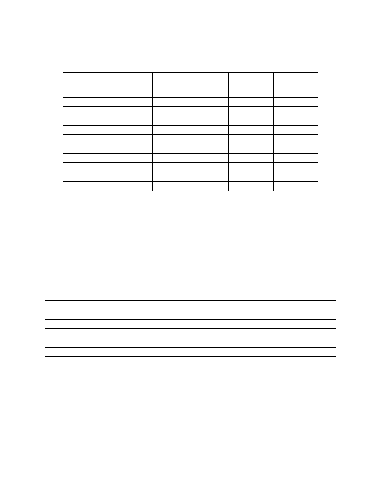
MOTOROLA CENTRAL PROCESSING UNIT M68HC11
6-14 REFERENCE MANUAL
6.3.1.4 Logical Operations
This group of instructions is used to perform the boolean logical operations AND, in-
clusive OR, exclusive OR, and one’s complement.
6.3.1.5 Data Testing and Bit Manipulation
This group of instructions is used to operate on operands as small as a single bit, but
these instructions can also operate on any combination of bits within any 8-bit location
in the 64-Kbyte memory space. The bit test (BITA or BITB) instructions perform an
AND operation within the CPU to update condition code bits without altering either op-
erand. The BSET and BCLR instructions read the operand, manipulate selected bits
within the operand, and write the result back to the operand address. Some care is re-
quired when read-modify-write instructions such as BSET and BCLR are used on I/O
and control register locations because the physical location read is not always the
same as the location written.
6.3.1.6 Shifts and Rotates
All the shift and rotate functions in the M68HC11 CPU involve the carry bit in the CCR
in addition to the 8- or 16-bit operand in the instruction, which permits easy extension
to multiple-word operands. Also, by setting or clearing the carry bit before a shift or ro-
tate instruction, the programmer can easily control what will be shifted into the opened
end of an operand. The arithmetic shift right (ASR) instruction maintains the original
value of the MSB of the operand, which facilitates manipulation of two’s-complement
(signed) numbers.
Function Mnemon-
ic IMM DIR EXT INDX INDY INH
AND A with Memory ANDA XXXXX
AND B with Memory ANDB XXXXX
Bit(s) Test A with Memory BITA XXXXX
Bit(s) Test B with Memory BITB XXXXX
One’s Complement Memory Byte COM X X X
One’s Complement A COMA X
One’s Complement B COMB X
OR A with Memory (Exclusive) EORA XXXXX
OR B with Memory (Exclusive) EORB XXXXX
OR A with Memory (Inclusive) ORAA XXXXX
OR B with Memory (Inclusive) ORAB XXXXX
Function Mnemonic IMM DIR EXT INDX INDY
Bit(s) Test A with Memory BITA XXXXX
Bit(s) Test B with Memory BITB XXXXX
Clear Bit(s) in Memory BCLR X X X
Set Bit(s) in Memory BSET X X X
Branch if Bit(s) Clear BRCLR X X X
Branch if Bit(s) Set BRSET X X X

M68HC11 CENTRAL PROCESSING UNIT MOTOROLA
REFERENCE MANUAL 6-15
The logical-left-shift instructions are shown in parentheses because there is no differ-
ence between an arithmetic and a logical left shift. Both mnemonics are recognized by
the assembler as equivalent, but having both instruction mnemonics makes some pro-
grams easier to read.
6.3.2 Stack and Index Register Instructions
The following table summarizes the instructions available for the 16-bit index registers
(X and Y) and the 16-bit stack pointer.
Function Mnemonic IMM DM EXT INDX INDY INH
Arithmetic Shift Left Memory ASL X X X
Arithmetic Shift Left A ASLA X
Arithmetic Shift Left B ASLB X
Arithmetic Shift Left Double ASLD X
Arithmetic Shift Right Memory ASR X X X
Arithmetic Shift Right A ASRA X
Arithmetic Shift Right B ASRB X
(Logical Shift Left Memory) (LSL) X X X
(Logical Shift Left A) (LSLA) X
(Logical Shift Left B) (LSLB) X
(Logical Shift Left Double) (LSLD) X
Logical Shift Right Memory LSR X X X
Logical Shift Right A LSRA X
Logical Shift Right B LSRB X
Logical Shift Right D LSRD X
Rotate Left Memory ROL X X X
Rotate Left A ROLA X
Rotate Left B ROLB X
Rotate Right Memory ROR X X X
Rotate Right A RORA X
Rotate Right B RORB X

MOTOROLA CENTRAL PROCESSING UNIT M68HC11
6-16 REFERENCE MANUAL
The exchange D with X (XGDX) and exchange D with Y (XGDY) provide a simple way
of transferring a pointer value from a 16-bit index register to accumulator D, which has
more powerful 16-bit arithmetic capabilities than the 16-bit index registers. Since these
are bidirectional exchanges, the original value of accumulator D is automatically pre-
served in the index register while the pointer is being manipulated in accumulator D.
When pointer calculations are finished, another exchange simultaneously updates the
index register and restores accumulator D to its former value.
The transfers between an index register and the stack pointer deserve additional com-
ment. The stack pointer always points at the next free location on the stack as opposed
to the last item that was pushed onto the stack. The usual reason for transferring the
stack pointer value into an index register is to allow indexed addressing access to in-
formation that was formerly pushed onto the stack. In such cases, the address pointed
to by the stack pointer is of no value since nothing has yet been stored at that location.
This fact explains why the value in the stack pointer is incremented during transfers to
an index register. There is a corresponding decrement of a 16-bit value as it is trans-
ferred from an index register to the stack pointer.
Function Mnemonic IMM DIR EXT INDX INDY INH
Add Accumulator B to X ABX X
Add Accumulator B to Y ABY X
Compare X to Memory (16 Bit) CPX X X X X X
Compare Y to Memory (16 Bit) CPY X X X X X
Decrement Stack Pointer DES X
Decrement Index Register X DEX X
Decrement Index Register Y DEY X
Increment Stack Pointer INS X
Increment Index Register X INX X
Increment Index Register Y INY X
Load Index Register X LDX X X X X X
Load Index Register Y LDY X X X X X
Load Stack Pointer LDS X X X X X
Pull X from Stack PULX X
Pull Y from Stack PULY X
Push X onto Stack PSHX X
Push Y onto Stack PSHY X
Store Index Register X STX X X X X X
Store Index Register Y STY X X X X X
Store Stack Pointer STS X X X X X
Transfer SP to X TSX X
Transfer SP to Y TSY X
Transfer X to SP TXS X
Transfer Y to SP TYS X
Exchange D with X XGDX X
Exchange D with Y XGDY X

M68HC11 CENTRAL PROCESSING UNIT MOTOROLA
REFERENCE MANUAL 6-17
6.3.3 Condition Code Register Instructions
These instructions allow a programmer to manipulate bits in the CCR.
Initially, it may appear that there should be a set and a clear instruction for each of the
eight bits in the CCR; however, these instructions are present for only three of the eight
bits (C, I, and V). Upon closer consideration, good reasons exist for not including the
set and clear instructions for the other five bits. The stop disable (S) bit is an unusual
case because this bit is intended to lock out the STOP instruction for those who view
it as an undesirable function in their application. Providing set and clear instructions
for this bit would make it easier to enable STOP when it was not wanted or disable
STOP when it was wanted. The TAP instruction provides a way to change the S bit but
reduces the chance of an undesirable change to S because the value of accumulator
A at the time the TAP instruction is executed determines whether the S bit will actually
change.
The XIRQ mask (X bit) is another unusual case. The definition of this bit specifically
states that software shall not be allowed to change X from zero to one; in fact, this
change is even prohibited by hardware logic. This feature immediately eliminates a
need for a set X instruction. For arguments similar to those used for the S bit, the TAP
instruction is preferred over a clear X instruction to clear X because TAP makes it a
little less likely that X will become cleared before the programmer intended.
The half-carry (H) bit needs no set or clear instructions because this condition code bit
is only used by the DAA instruction to adjust the result of a BCD add or subtract. Since
the H bit is not used as a test condition for any branches, it would not be useful to be
able to set or clear this bit.
This leaves only the negative (N) and zero (Z) condition code bits. In contrast to S, X,
and H, it is often useful to be able to easily set or clear these flag bits. A clear accu-
mulator instruction, such as CLRB, will clear the N and set the Z condition code bits.
The load instruction, ;LDAA#$80, causes N to be set and Z to be cleared. Since there
are so many simple instructions that can set or clear N and Z, it is not necessary to
provide specific set and clear instructions for N and Z in this group.
6.3.4 Program Control Instructions
This group of instructions, which is used to control the flow of a program rather than to
Function Mnemonic INH
Clear Carry Bit CLC X
Clear Interrupt Mask Bit CLI X
Clear Overflow Bit CLV X
Set Carry Bit SEC X
Set Interrupt Mask Bit SEI X
Set Overflow Bit SEV X
Transfer A to CCR TAP X
Transfer CCR to A TPA X

MOTOROLA CENTRAL PROCESSING UNIT M68HC11
6-18 REFERENCE MANUAL
manipulate data, has been divided into five subgroups: 1) branches, 2) jumps, 3) sub-
routine calls and returns, 4) interrupt handling, and 5) miscellaneous,
6.3.4.1 Branches
These instructions allow the CPU to make decisions based on the contents of the con-
dition code bits. All decision blocks in a flow chart would correspond to one of the con-
ditional branch instructions summarized in the following table.
The limited range of branches (–128/+127 locations) is more than adequate for most
(but not all) situations. In cases where this range is too short, a jump instruction must
be used. For every branch, there is a branch for the opposite condition; thus, it is sim-
ple to replace a branch having an out-of-range destination with a sequence consisting
of the opposite branch around a jump to the out-of-range destination. For example, if
a program contained the following instruction
BHI TINBUK2 Unsigned >
where TINBUK2 was out of the –128/+127 location range, the following instruction se-
quence could be substituted:
BLS AROUND Unsigned ≤
JMP TINBUK2 Still go to TINBUK2 if >
AROUND EQU *
Function Mnemonic REL DIR INDX INDY Comments
Branch if Carry Clear BCC X C = 0 ?
Branch if Carry Set BCS X C = 1 ?
Branch if Equal Zero BEQ X Z = 1 ?
Branch if Greater Than or Equal BGE X Signed ≥
Branch if Greater Than BGT X Signed >
Branch if Higher BHI X Unsigned >
Branch if Higher or Same (same as BCC) BHS X Unsigned ≥
Branch if Less Than or Equal BLE X Signed ≤
Branch if Lower (same as BCS) BLO X Unsigned <
Branch if Lower or Same BLS X Unsigned ≤
Branch if Less Than BLT X Signed <
Branch if Minus BMI X N= 1 ?
Branch if Not Equal BNE X Z = 0 ?
Branch if Plus BPL X N = 0 ?
Branch if Bit(s) Clear in Memory Byte BRCLR X X X Bit Manipulation
Branch Never BRN X 3-cycle NOP
Branch if Bit(s) Set in Memory Byte BRSET X X X Bit Manipulation
Branch if Overflow Clear BVC X V = 0 ?
Branch if Overflow Set BVS X V = 1 ?
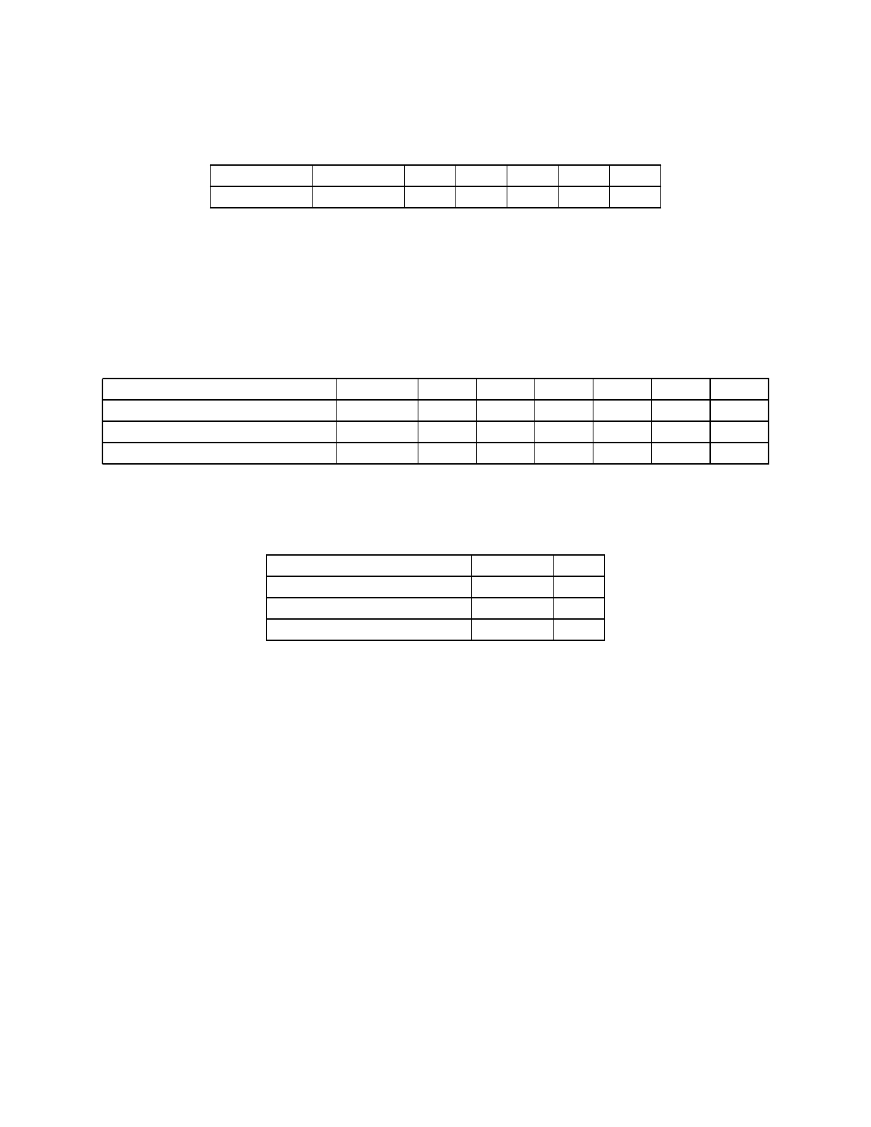
M68HC11 CENTRAL PROCESSING UNIT MOTOROLA
REFERENCE MANUAL 6-19
6.3.4.2 Jumps
The jump instruction allows control to be passed to any address in the 64-Kbyte mem-
ory map.
6.3.4.3 Subroutine Calls And Returns (BSR, JSR, RTS)
These instructions provide an easy way to divide a programming task into manageable
blocks called subroutines. The CPU automates the process of remembering the ad-
dress in the main program where processing should resume after the subroutine is fin-
ished. This address is automatically pushed onto the stack when the subroutine is
called and is pulled off the stack during the RTS instruction that ends the subroutine.
6.3.4.4 Interrupt Handling (RTI, SWI, WAI)
This group of instructions is related to interrupt operations.
The software interrupt (SWI) instruction is similar to a JSR instruction, except the con-
tents of all working CPU registers are saved on the stack rather than just the return
address. SWI is unusual in that it is requested by the software program as opposed to
other interrupts that are requested asynchronously to the executing program.
Wait for interrupt (WAI) has two main purposes. WAI is executed to place the MCU in
a reduced power-consumption standby state (WAIT mode) until some interrupt occurs.
It is also used to reduce the latency time to some important interrupt. The reduction of
latency occurs because the time-consuming task of storing the CPU registers on the
stack is performed as soon as the WAI instruction begins executing. When the inter-
rupt finally occurs, the CPU is ready to fetch the appropriate vector so the delay asso-
ciated with register stacking is eliminated from latency calculations.
6.3.4.5 Miscellaneous (NOP, STOP, TEST)
NOP, which can be used to introduce a small time delay into the flow of a program, is
often useful in meeting the timing requirements of slow peripherals. By incorporating
NOP instructions into loops, longer delays can be produced.
Function Mnemonic DIR EXT INDX INDY INH
Jump JMP XXXX
Function Mnemonic REL DIR EXT INDX INDY INH
Branch to Subroutine BSR X
Jump to Subroutine JSR X X X X
Return from Subroutine RTS X
Function Mnemonic INH
Return from Interrupt RTI X
Software Interrupt SWI X
Wait for Interrupt WAI X

MOTOROLA CENTRAL PROCESSING UNIT M68HC11
6-20 REFERENCE MANUAL
During debugging, it is common to replace various instructions with NOP opcodes to
effectively remove an unwanted instruction without having to rearrange the rest of the
program. By using the memory modify function of a debug monitor, the instruction can
easily be removed and restored to see the effect.
Occasionally, a programmer is faced with the problem of fine-tuning the delays
through various paths in his program. In such cases, it is sometimes useful to use a
branch never (BRN) instruction as a three-cycle NOP. It is also possible to fine-tune
execution time by choosing alternate addressing-mode variations of instructions to
change the execution time of an instruction sequence without changing the program’s
function.
STOP is an unusual instruction because it causes the oscillator and all MCU clocks to
freeze. This frozen state is called STOP mode, and power consumption is dramatically
reduced in this mode. The operation of this instruction is also dependent upon the S
condition code bit because the STOP mode is not appropriate for all applications. If S
is one, the STOP instruction is treated as a NOP instruction, and processing continues
to the next instruction.
The TEST instruction is used only during factory testing and is treated as an illegal op-
code in normal operating modes of the MCU. This instruction causes unusual behavior
on the address bus (counts backwards), which prevents its use in any normal system.
Function Mnemonic INH
No Operation (2-cycle delay) NOP X
Stop Clocks STOP X
Test TEST X

M68HC11 PARALLEL INPUT/OUTPUT MOTOROLA
REFERENCE MANUAL 7-1
SECTION 7
PARALLEL INPUT/OUTPUT
This section describes parallel I/O operations in the MC68HC11A8, which includes
port reads and writes as well as strobe and handshake operations on ports B and C.
The section begins with an overview, followed by detailed descriptions of each port
and the handshake I/O subsystem. A number of schemes for efficient use of parallel
I/O on the MC68HC11A8 are included.
7.1 Parallel I/O Overview
The MC68HC11A8 has a total of 40 I/O pins, which will be discussed in 7.3 Detailed
I/O Pin Descriptions. All these pins are shared between general-purpose I/O usage
and at least one other on-chip peripheral function. Although the following paragraphs
are primarily concerned with the general-purpose I/O capabilities of these pins, some
important interactions with the alternate functions will be discussed.
Shared functions of port A include general-purpose I/O, the main timer system, and
the pulse accumulator system. Port A has three fixed-direction input pins, four fixed-
direction output pins, and one bidirectional pin. The direction of the PA7 pin is con-
trolled by the data direction register A bit 7 control bit (DDRA7) in the pulse accumu-
lator control (PACTL) register. Port A data is read from and written to the PORTA
register. Meaningful data may be read from port A even when the pins are configured
for an alternate timer or pulse accumulator function. Data written to port A does not
directly affect port A pins configured for an alternate timer output function, but the data
is remembered in an internal latch so that, if the alternate function is disabled later, the
last data written to port A will be driven out of the associated output pin.
Ports B and C and the strobe A (STRA) and strobe B (STRB) pins should be consid-
ered together because their function depends on the basic operating mode of the
MC68HC11A8. When the microcontroller unit (MCU) is operating in a single-chip
mode, these 18 pins are used for general-purpose I/O and for the handshake I/O sub-
system. When the MCU is operating in an expanded mode, these pins are used for a
multiplexed address/data bus. The handshake and general-purpose I/O functions,
which are lost in the expanded mode, can be regained by use of the MC68HC24 port
replacement unit. Special care was taken in designing both these parts so that soft-
ware could be developed on an expanded system using these two parts and then later
be mask programmed into the read-only memory (ROM) of an MC68HC11A8, which
will be used in single-chip mode. Although care was taken to assure that the expanded
system with an MC68HC24 would work exactly like the MC68HC11A8 in single-chip
mode, there are a few subtle differences. For the vast majority of applications, these
differences are irrelevant. For the benefit of those rare cases where a problem could
arise, the differences will be explained in the detailed descriptions of these ports and
pins in 7.3 Detailed I/O Pin Descriptions.

MOTOROLA PARALLEL INPUT/OUTPUT M68HC11
7-2 REFERENCE MANUAL
Port B is a general-purpose, 8-bit, fixed-direction output port. Writes to the port B reg-
ister (PORTB) cause data to be latched and driven out of the port B pins. Reads of
PORTB return the last data that was written to port B. When the handshake I/O sub-
system is operating in simple strobed mode, writes to PORTB automatically cause a
pulse on the STRB output pin. The simple strobe mode is selected by the handshake
(HNDS) control bit equal to zero in the parallel I/O control (PIOC) register.
Port C is a general-purpose, 8-bit, bidirectional I/O port. The primary direction of data
flow at each port C pin is independently controlled by a corresponding bit in the data
direction control register for port C (DDRC). In addition to normal I/O functions at port
C, there is an independent, 8-bit, parallel latch that captures port C data whenever a
selected active edge is detected on the STRA input pin. Reads of PORTCL return the
contents of this port C latch; whereas, reads of PORTC return the current data from
port C. Writes to either PORTC or PORTCL cause the written data to be driven out of
port C output pins; however, PORTCL writes also trigger output handshake sequenc-
es; PORTC writes do not. Writes to port C pins not configured as outputs do not cause
data to be driven out of those pins, but the data is remembered in internal latches;
thus, if the pins later become outputs, the last data written to PORTC or PORTCL will
be driven out the port C pins.
Port C can be configured for wired-OR operation by setting the port C wired-OR mode
(CWOM) control bit in the PIOC register. This procedure disables the P-channel pull-
up drivers of port C output pins and allows port C pins to be directly connected to each
other or to other open-drain-type pins. In this configuration, there is no danger of de-
structive conflicts if two output drivers try to drive the same node at the same time. As
with any open-drain line, an external pull-up resistor is required.
Whenever the handshake I/O subsystem is configured for a full-handshake mode, port
C is used for parallel data input or output. STRA is a strobe input pin that causes port
C data to be captured when a selected edge is detected. In the three-state variation of
full-output handshake, the STRA pin also acts as an output enable control to force port
C pins to be driven outputs while STRA is in its selected state. STRB is a strobe output
pin that can be used in a pulsed or interlocked configuration. In the pulsed configura-
tion, some action in the handshake I/O subsystem initiates STRB, which then stays
active for two E-clock cycles before reverting to its inactive state. In the interlocked
configuration, STRB is initiated by one action in the handshake subsystem and termi-
nated by a separate action. The final major element of the handshake subsystem is
the strobe A flag (STAF) status bit. STAF is always set upon recognition of the select-
ed edge at the STRA pin, but the action that clears STAF depends on the handshake
mode. There is a more detailed description of the handshake I/O subsystem in 7.4
Handshake I/O Subsystem.
Port D is a general-purpose, 6-bit, bidirectional data port. Two port D pins are alter-
nately used by the asynchronous serial communications interface (SCI) subsystem.
The remaining four port D pins are alternately used by the synchronous serial periph-
eral interface (SPI) subsystem. The primary direction of data flow at each of the port
D pins is selected by a corresponding bit in the data direction register for port D
(DDRD). Port D can be configured for wired-OR operation by setting the port D wired-
M68HC11 PARALLEL INPUT/OUTPUT MOTOROLA
REFERENCE MANUAL 7-3
OR mode control bit (DWOM) in the SPI control register (SPCR).
Port E is an 8-bit, fixed-direction input port. Port E pins alternately function as analog-
to-digital (A/D) converter channel inputs. Port E input buffers are specially designed
so they will not draw excessive power-supply currents when their inputs are driven by
intermediate levels.
7.2 Parallel I/O Register And Control Bit Explanations
Figure 7-1 shows all the registers and control bits concerned with the discussion of
parallel I/O in the following paragraphs. The registers are shown in the order they ap-
pear in the memory map of the MC68HC11A8 because this order is significant in the
case of double-byte reads and writes. Figure 7-2 shows a number of registers and
control bits mentioned in 7.3 Detailed I/O Pin Descriptions. These control bits are
used to enable other on-chip peripheral subsystems to use the I/O pins. These regis-
ters, which are shown here for reference, are discussed throughout this manual. Bit
positions labeled with a zero rather than a name indicate unimplemented bits that al-
ways read as zeros.
Figure 7-1 Parallel I/O Registers and Control Bits
Bit 7 654321Bit 0
$1000 Bit 7 ——————Bit 0 PORTA
$1002 STAF STAI CWOM HNDS OIN PLS EGA INVB PIOC
$1003 Bit 7 ——————Bit 0 PORTC
$1004 Bit 7 ——————Bit 0 PORTB
$1009 0 0 Bit 5 ————Bit 0 DDRD
$1026 DDRA7 PAEN PAMOD PEDGE 0 0 RTR1 RTR0 PACTL
$1028 SPIE SPE DWOM MSTR CPOL CPHA SPR1 SPR0 SPCR

MOTOROLA PARALLEL INPUT/OUTPUT M68HC11
7-4 REFERENCE MANUAL
Figure 7-2 Pin Logic Registers and Control Bits
The addresses for the registers in Figure 7-1 and Figure 7-2 are in the form "$10xx"
where xx is a hexadecimal number between 00 and 3F. The "1" indicates that the most
significant hexadecimal digit is a variable controlled by user software. The RAM and I/
O mapping (INIT) register is used to specify the location of internal registers and RAM.
By default, RAM is located from $0000 to $00FF, and registers are located from $1000
to $103F at reset. The user can elect to move either one or both of these resources by
writing a new value into the INIT register within 64 bus cycles after reset. The INIT reg-
ister is discussed in greater detail in SECTION 4 ON-CHIP MEMORY.
The bit-manipulation instructions in the MC68HC11A8 can only be used in zero-page
or indexed addressing modes. To use indexed addressing mode to access internal
registers, the user would first set either the X or Y index register equal to the base ad-
dress of the registers (usually $1000). To use the zero-page addressing mode, the
user would first remap the internal registers by writing to the INIT register during reset
initialization.
7.2.1 Port Registers
Reads of port registers will return either the level at the pin itself or the logic state at a
point inside the output pin buffer. Usually, the state of the corresponding DDR bit will
determine which of these points will be used for a read if a choice exists. Refer to 7.3
Detailed I/O Pin Descriptions for more specific information. Writes to port registers
cause the written data to be latched and driven out of the corresponding port output
pins.
If a port pin is capable of being an output, this written information is latched even if the
pin is not configured as a port output at the time of the write. If the pin is subsequently
reconfigured to be a port output, the output pin will be driven with the last data that was
written to that port. Writes to port bits that are fixed-direction input pins have no mean-
ing or effect.
PORTCL, a special port register associated with port C, is part of the handshake I/O
subsystem. Reads of this address return data from an 8-bit port C latch. The inputs to
Bit 7 654321Bit 0
$100B FOC1 FOC2 FOC3 FOC4 FOC5 0 0 0 CFORC
$100C OC1M7 OC1M6 OC1M5 OC1M4 OC1M3 0 0 0 OC1M
$100D OC1D7 OC1D6 OC1D5 OC1D4 OC1D3 0 0 0 OC1D
$1020 OM2 OL2 OM3 OL3 OM4 OL4 OM5 OL5 TCTL1
$103D RAM3 RAM2 RAM1 RAM0 REG3 REG2 REG1 REG0 INIT

M68HC11 PARALLEL INPUT/OUTPUT MOTOROLA
REFERENCE MANUAL 7-5
this port C latch are connected to the port C pins, and the latches are clocked when a
selected edge is recognized at the STRA pin. Contrary to first impressions, writes to
PORTCL do not change the data in the port C latch register. Instead, writes to
PORTCL are used as an alternate way to write data to port C. In addition to writing
data to the port C output latches, writes to PORTCL also trigger special handshake
sequences in the handshake I/O subsystem, which allows some port C pins to be
treated as general-purpose outputs while others are being used for full-handshake
outputs. A user would write data to PORTC to change the non-handshake pins in port
C. To change the data on a full-handshake pin of port C, the user would write to
PORTCL.
7.2.2 Data Direction Registers
These registers and control bits are used to specify the primary direction of data flow
at each bidirectional port pin. A zero in a data direction register (DDR) bit disables the
output buffer for that pin so the pin is configured as an input. When a DDR bit is set to
one, it enables the output driver for the associated port pin so the pin is configured as
an output. During reset, internal logic in the MC68HC11A8 forces all DDR bits to zero;
thus, all bidirectional I/O pins are configured as high-impedance inputs until they are
reconfigured by software.
In some cases, an enabled on-chip subsystem can override the DDR bit and force a
pin to be an input or an output. For example, it is illogical for the TxD pin to be config-
ured as an input while the SCI transmitter is using this pin. Whenever the SCI trans-
mitter subsystem is enabled, the TxD pin is configured as an output, regardless of
what the corresponding DDRD bit is. There is a subtle benefit to this override besides
the obvious savings gained by not having to write to the DDR. Depending on the over-
all system attached to the TxD pin, it may be desirable for this pin to revert to a specific
driven logic level or to a high-impedance condition. If the DDR bit is zero, the TxD pin
will revert to a general-purpose, high-impedance input pin when not being used by the
transmitter. If the DDR bit is one, the TxD pin will revert to a general-purpose output
pin, and the driven logic level will reflect what was last written to bit 1 of port D.
In other cases, the DDR bits continue to affect the configuration of a port pin even after
an on-chip subsystem has been enabled to use the pin. Consider the SPI bidirectional
data pins master in/slave out (MISO) and master out/slave in (MOSI). Although the
MC68HC11A8 SPI system is capable of full-duplex operation, some synchronous se-
rial protocols are configured for half-duplex operation with a single, bidirectional data
line. For the MC68HC11A8 to operate in such a system, it must be able to selectively
disable its MOSI and MISO outputs.
The state of a DDR bit influences the source of data when the corresponding port bit
is read. In general, when a pin is configured as an input, reads return the logic level
from the pin itself. When a pin is configured as an output, reads return a value corre-
sponding to the level at the inside of the output buffer for that pin. This fact is especially
important in the case of pins configured for wired-OR operation or for the three-state
variation of full-output handshake at port C. In these cases, the value at the pin itself
does not necessarily reflect the value last written to the port; therefore, it is important
to read the level inside the output buffer rather than the level at the pin.
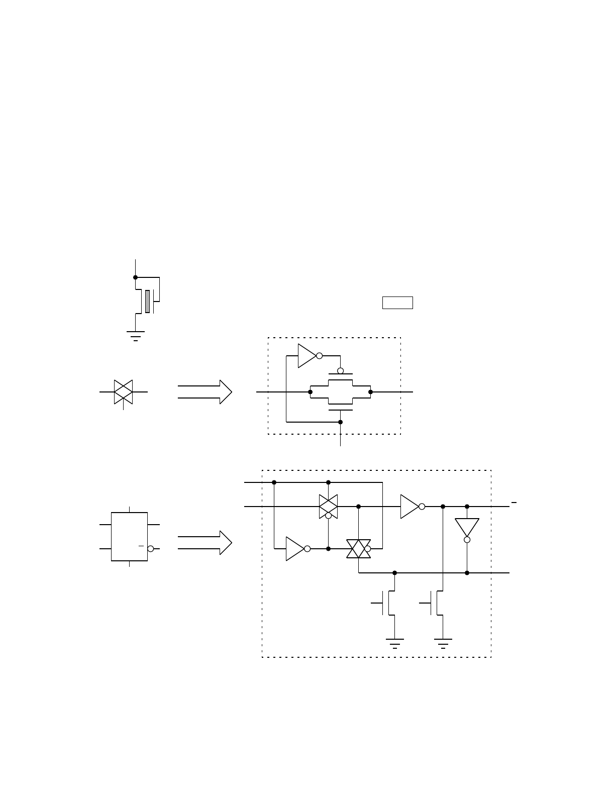
MOTOROLA PARALLEL INPUT/OUTPUT M68HC11
7-6 REFERENCE MANUAL
7.3 Detailed I/O Pin Descriptions
The logic associated with each of the I/O pins is described in detail in the following
paragraphs. All circuitry directly connected to a pin is shown exactly as it is implement-
ed in the MC68HC11A8. Logic not directly connected to a pin is functionally accurate,
but the drawings have been simplified. Figure 7-3 shows some of the symbols used
in the logic drawings, which may not be familiar to all readers. The protection devices,
which are intended to protect the MC68HC11A8 from high-voltage transients, have no
effect while pins are within the VSS to VDD range. Although transmission gates are ac-
tually full CMOS bidirectional switches, they are shown in simplified form in the logic
diagrams. Half flip-flops (HFFS) are latches that are transparent while the clock input
is high and are latched while the clock input is low. Set and reset inputs are optional
on HFFS. Any name enclosed in a rectangle indicates a control bit within the
MC68HC11A8. Numbers in square brackets are references for the text descriptions.
Figure 7-3 Special Symbols used in Pin Logic Diagrams
DDRA7
[3] — REFERENCE NUMBER
— CONTROL BIT
PROTECTION
THICK-FIELD
PROTECTION
DEVICE
TRANSMISSION GATE
HALF FLIP-FLOP
RS
Q
Q
C
D
D
CQ
Q
S
HFF
R
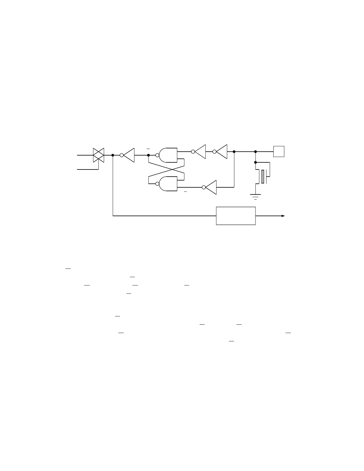
M68HC11 PARALLEL INPUT/OUTPUT MOTOROLA
REFERENCE MANUAL 7-7
7.3.1 Port A
The eight port A pins can be independently configured for general-purpose I/O or for
timer or pulse accumulator functions. The following paragraphs describe the pin logic
for port A pins. The idealized timing for critical port A signals is presented in 7.3.1.4
Port A Idealized Timing.
7.3.1.1 PA[2:0] (IC[3:1]) Pin Logic
Refer to Figure 7-4 for the following discussion. The cross-coupled NAND circuit with
four associated inverters is a hysteresis buffer. Hysteresis is provided by sizing invert-
er [1] so its switch point is higher than normal and by sizing inverter [2] so its switch
point is lower than normal.
Figure 7-4 PA[2:0] (IC[3:1]) Pin Logic
Starting with zero on the pin, a slowly rising signal causes inverter [2] to switch so that
the R signal goes to an inactive-high state. As the input continues to rise, inverter [1]
switches, causing a low S, which causes the cross-coupled NAND latch to set Q high
and clear Q low. The low Q reinforces the S signal so that, even if noise causes invert-
er [1] to switch back to S equals one, the cross-coupled latch will not reset.
Conversely, starting with one on the pin, a slowly failing signal causes inverter [1] to
switch, causing the S signal to be placed in an inactive-high state. As the input contin-
ues to fall, inverter [2] switches, causing a low R. This low R resets the cross-coupled
NAND latch, setting Q high and clearing Q low. The low Q reinforces the R signal so
that, even if noise causes inverter [2] to switch back to R equals one, the cross-cou-
pled latch will not become set.
For bits 0, 1, and 2, port A reads return the buffered states of the corresponding pins.
Port A reads are completely independent of timer input-capture functions.
7.3.1.2 PA[6:3] (OC[5:2]) Pin Logic
Refer to Figure 7-5 for the following discussion. For bits 3, 4, 5, and 6, port A reads
return the logic state from a point inside the output pin buffer. During a port A read,
transmission gate [1] is enabled to couple logic state [2] to the internal data bus.
PIN
[3]
PROTECTION
TIMER
INPUT-CAPTURE
EDGE DETECT
Q
QPA2–PA0
(IC1–IC3)
D2–D0
RPORTA
R
S
[2]
[1]
IC1–IC3
TRIGGER

MOTOROLA PARALLEL INPUT/OUTPUT M68HC11
7-8 REFERENCE MANUAL
Inverter [2] is driven by a head-to-tail cheater latch. The feedback inverter [3] in this
cheater latch is sized to be overridden by transmission gate [4], [5], or [6]. These three
transmission gates correspond to the three possible sources of data for these port A
pins as follows. General-purpose port A outputs come through transmission gate [4]
from HFF latch [7]. Output compares 5 through 2 (OC[5:2]) affect their corresponding
port A pin via transmission gate [6]; output compare 1 (OC1) can affect these port A
pins via transmission gate [5].
Control gate [8] enables general-purpose port A outputs during PTACLK when no tim-
er function is enabled to control this pin. PTACLK is an internal clock signal that syn-
chronizes port A pin changes to the falling edge of E. OC1 is enabled when the
corresponding OC1Mx bit is one, which disables control gate [8] and enables control
gate [9]. The OC[5:2] functions are enabled to control their corresponding port A pin
by the OMx:OLx bits not equal to 0:0. When OMx:OLx are not 0:0, control gate [8] is
disabled and control gate [10] is enabled.
Control gate [9] allows OC1 to affect this port A pin. When the corresponding OC1Mx
control bit is one, control gate [9] is enabled. The PTACLK clock signal acts as a
strobe. When there is a successful OC1 compare (OC1CMP) or when OC1 is forced
by FOC1 equals one, control gate [9] enables transmission gate [5], which causes the
corresponding OC1Dx state to be transferred to cheater latch [3]. NAND gate [11] pro-
vides a disable to control gate [10] so that if OC1 and another output compare simul-
taneously attempt to change the same port A pin, OC1 will override.
Control gate [10] is enabled by the corresponding OMx:OLx control bits not equal to
0:0. When there is a successful output compare x (OCxCMP) or when OCx is forced
by FOCx equals one, control gate [10] enables transmission gate [6] and momentarily
disables transmission gate [12]. Transmission gate [12] transfers the previous port A
pin state to cheater latch [14]. Cheater latch [14] holds the previous pin state stable for
logic [13] while transmission gate [12] is disabled and transmission gate [6] is enabled.
Set-reset (S/R) latch [13] and associated logic is used to determine the next timer out-
put state that would result from a successful OCx compare. This next timer output
state is determined by the states of the associated OMx and OLx control bits and the
previous port A pin state.
7.3.1.3 PA7 (OC1, PAI) Pin Logic
Refer to Figure 7-6 for the following discussion. Hysteresis buffer [1] was previously
described in 7.3.1.1 PA[2:0] (IC[3:1]) Pin Logic. Reads of port A bit 7 always return
the buffered state of the PA7 pin. For this bidirectional I/O pin, the state of the corre-
sponding DDR control bit has no effect on the source of the data for the read. During
a port A read, transmission gate [2] is enabled so the buffered state of the PA7 pin is
driven onto the internal data bus.
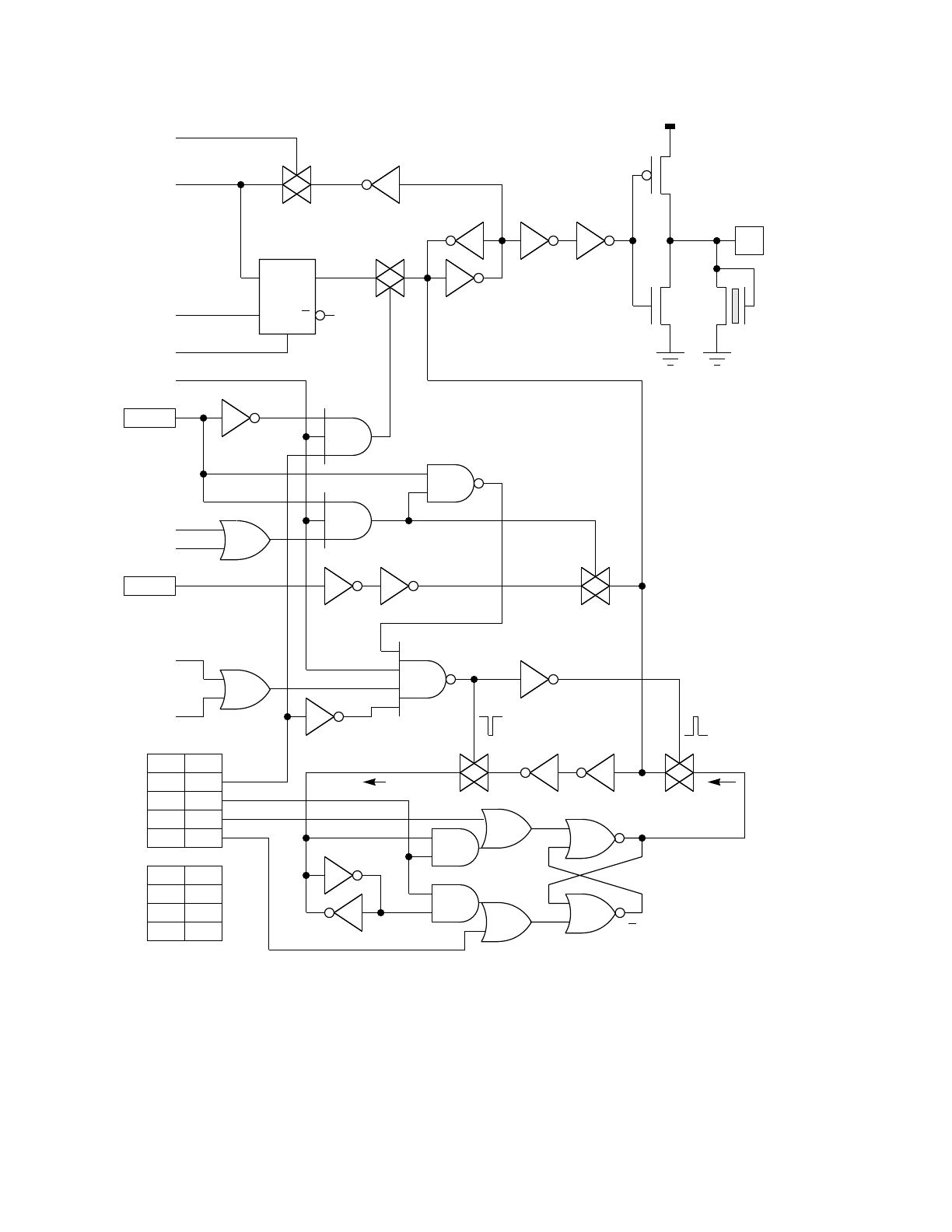
M68HC11 PARALLEL INPUT/OUTPUT MOTOROLA
REFERENCE MANUAL 7-9
Figure 7-5 PA[6:3] (OC[5:2]) Pin Logic
Q
Q
R
S
[12]
[13]
[6]
[9]
[5]
[10]
[14]
[11]
[8]
[7]
[1]
[3]
[4]
[2]
DISABLE
TOGGLE
CLEAR
SET
11
01
10
00
OLxOLx
OL2OM2
OL3OM3
OL4OM4
OL5OM5
NEXT TIMER
OUT STATE
PREVIOUS
TIMER OUT
STATE
PA6–PA3
(OC2–OC5)
FOCx
x=5,4,3,2
OCxCMP
x=5,4,3,2
PTACLK
FOC1
x=5,4,3,2
OC1CMP
x=5,4,3,2
RST
WPORTA
D6–D3
RPORTA
D
C
Q
Q
HFFR
R
VDD
PROTECTION
PIN
N
P
OC1Dx
OC1Mx
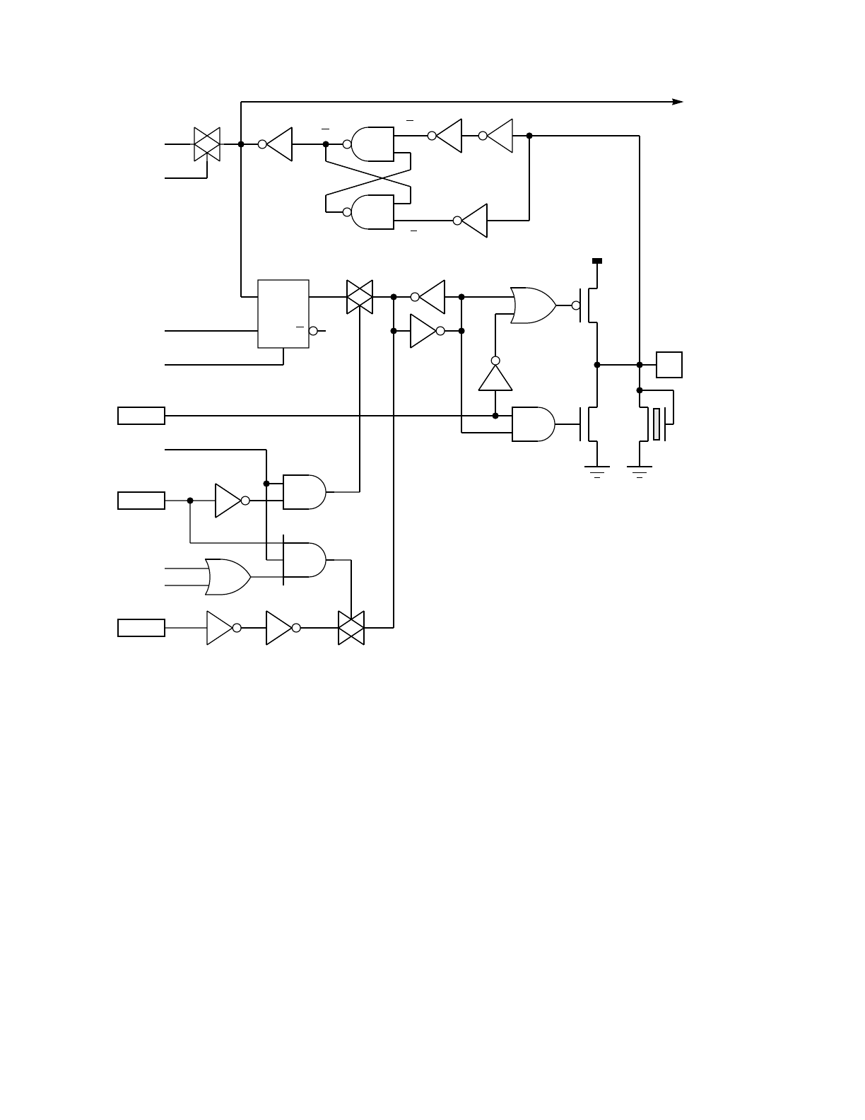
MOTOROLA PARALLEL INPUT/OUTPUT M68HC11
7-10 REFERENCE MANUAL
Figure 7-6 PA7 (OC1, PAI) Pin Logic
Output buffer [3] is enabled when DDRA7 is one. When DDRA7 is zero, the N- and P-
channel drivers are disabled so the PA7 pin acts as a high-impedance input. Data for
the PA7 pin is held in cheater latch [4]. Transmission gates [5] and [6] correspond to
the two possible sources of output data for the PA7 pin.
When the OC1M7 control bit is zero, control gate [9] is disabled and control gate [8] is
enabled. Control gate [8] enables transmission gate [5] so general-purpose output
data from HFF [7] is transferred to cheater latch [4]. A write to port A causes data to
be written into HFF [7], which is cleared to zero during reset.
When the OC1M7 control bit is one, control gate [8] is disabled and control gate [9] is
enabled. While control gate [9] is enabled, a successful OC1 compare (OC1CMP) or
a force OC1 (FOC1) will enable transmission gate [6]. Transmission gate [6] causes
the OC1D7 state to be transferred to cheater latch [4].
Q
Q
D7
RPORTA
R
S
[2] [1]
[5]
[7]
[6]
[3]
[4] PA7
(PAI)
RST
WPORTA
OC1CMP
D
C
Q
Q
HFFR
R
VDD
PROTECTION
PIN
N
P
PTACLK
OC1M7
FOC1
[9]
[8]
OC1D7
DDRA7
TO PULSE
ACCUMULATOR
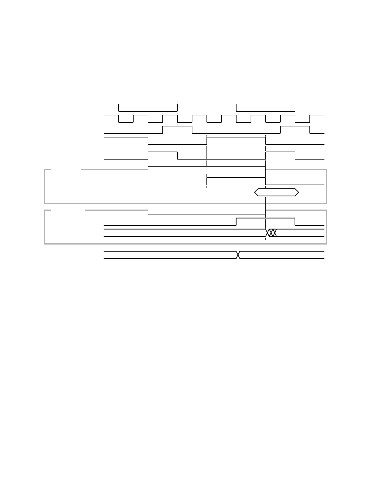
M68HC11 PARALLEL INPUT/OUTPUT MOTOROLA
REFERENCE MANUAL 7-11
7.3.1.4 Port A Idealized Timing
Figure 7-7 shows the idealized timing for important port A control signals. This timing
diagram, which does not consider any propagation delays, cannot be used as a sub-
stitute for data-sheet timing specifications. This information is useful for understanding
the basis for data-sheet timing specifications so timing information can be extrapolated
for bus frequencies other than that used for the data sheet.
Figure 7-7 Idealized Port A Timing
On a port A read, the RPORTA signal enables transmission gates driving port A data
onto the internal data bus. After the RPORTA signal is negated, data is held stable on
the self-latching internal data bus. The central processing unit (CPU) actually requires
this data to be valid for a setup and hold time around the rising edge of the internal
PH2 clock signal.
All operations that can cause changes to the port A output pins (except DDRA7 control
bit changes) are synchronized to the falling edge of the E clock. Changes to DDRA7
cause port A pins to change state at the falling edge of the internal PH2 clock.
7.3.2 Port B
The eight port B pins are fixed-direction output pins. When the MC68HC11A8 is oper-
ating in an expanded mode, port B is used for high-order address outputs. In single-
chip modes, port B is used for general-purpose output or for simple strobe output. The
following paragraphs describe the port B pin logic and the idealized timing for selected
port B signals.
NEW PORT A DATA
VALID DATA REQUIRED AT CPU
WRITE TO PORT A
READ FROM PORT A
PH2 (INTERNAL)
EXTAL
AS
PTACLK
PORT A INPUT
RPORTA
PORT A OUTPUT
WPORTA
PORT A OUTPUT PINS
CONTROL BIT CHANGES
FOR BITS: OC1Mx, OC1Dx,
OMx, OLx, DDRA7, FOCx
E
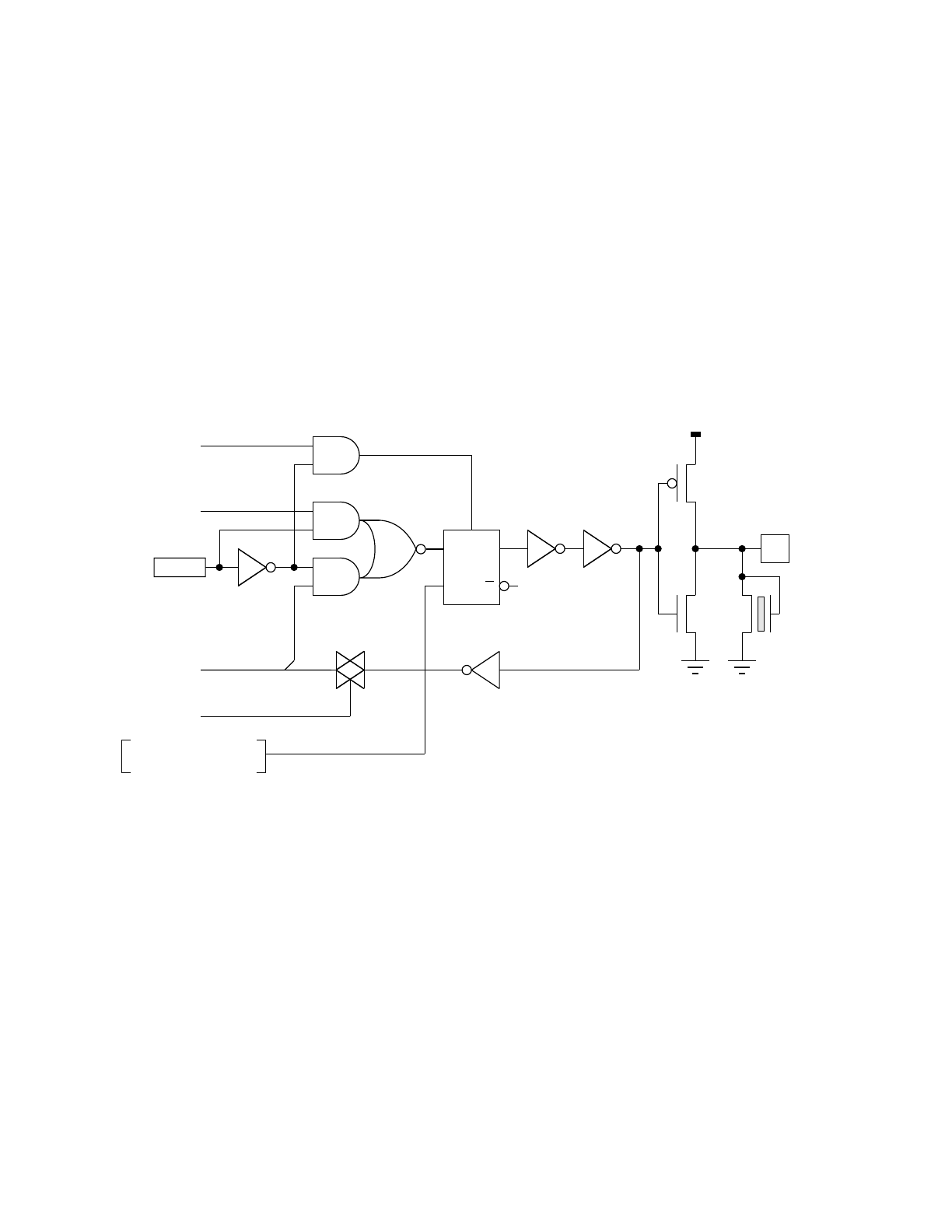
MOTOROLA PARALLEL INPUT/OUTPUT M68HC11
7-12 REFERENCE MANUAL
When the MC68HC11A8 is operating in an expanded mode, reads and writes to the
port B address are treated as external accesses to allow port B functions to be emu-
lated with external logic. The MC68HC24 port replacement unit (PRU) duplicates the
general-purpose and handshake I/O functions of ports B and C and the STRA and
STRB pins. The MC68HC24 connects to the multiplexed address/data bus of the
MC68HC11A8.
7.3.2.1 Port B Pin Logic
Refer to Figure 7-8 for the following discussion. Reads of port B return the logic state
from a point inside the output pin buffer. During reads of port B, transmission gate [1]
is enabled by the RPORTB signal to couple logic state [2] to the internal data bus. The
RPORTB signal is not asserted for port B reads in expanded modes since port B is an
external address in that case.
Figure 7-8 Port B Pin Logic
In single-chip modes, the mode A (MDA) control bit is zero, which enables AND gate
[3] and disables AND gate [4]. The internal data bus is coupled through AND gate [3]
and clocked into HFF [5] by the write port B (WPORTB) signal. The output of HFF [5]
is buffered and driven out the port B pins. In single-chip modes, HFF [5] is set to one
by AND gate [6] during reset, which results in logic zero at the port B pins.
In expanded modes, the MDA control bit is one, enabling AND gate [4] and disabling
AND gate [3], which couples high-order addresses to HFF [5]. In expanded modes,
HFF [5] is transparent while address strobe (AS) is high and latched while AS is low.
The output of HFF [5] is buffered and driven out the port B pins.
[5]
[1]
[2]
PB7–PB0
EXPANDED — AS
SINGLE CHIP — WPORTB
VDD
PROTECTION
PIN
N
P
MDA
Q
D
C
Q
S
HFFS
[3]
[4]
[6]
RST
A15–A8
D7–D0
RPORTB
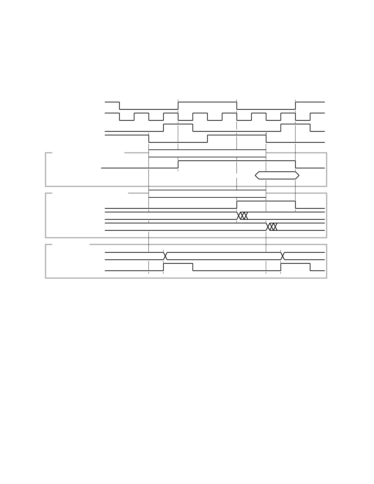
M68HC11 PARALLEL INPUT/OUTPUT MOTOROLA
REFERENCE MANUAL 7-13
7.3.2.2 Port B Idealized Timing
Figure 7-9 shows the idealized timing for important port B control signals. This timing
diagram, which does not consider any propagation delays, cannot be used as a sub-
stitute for data-sheet timing specifications. This information is useful for understanding
the basis for data-sheet timing specifications so timing information can be extrapolated
for bus frequencies other than that used for the data sheet.
Figure 7-9 Idealized Port B Timing
On a port B read, the RPORTB signal enables transmission gates, which drive port B
data onto the internal data bus. There is no case where port B data can change in the
same cycle in which a port B read is occurring. Port B writes cause changes to the port
B output pins at the falling edge of the internal PH2 clock. This edge corresponds to
the middle of the E-clock high time.
Although this section is not specifically concerned with expanded-mode operation of
port B, it is included here for reference. A more detailed discussion of the expansion
bus is included in 2.6 Typical Expanded-Mode-System Connections. Port B logic
provides a full one-eight-cycle hold time on the high-order addresses relative to the
falling edge of E.
7.3.2.3 Special Considerations For Port B On MC68HC24 PRU
The external PRU does not have access to the internal PH2 clock of the
NEW PORT B DATA
VALID DATA REQUIRED AT CPU
WRITE TO PORT B
READ FROM PORT B
PH2 (INTERNAL)
EXTAL
AS
PORT B INPUT (SINGLE-CHIP MODE)
RPORTB
PORT B OUTPUT (SINGLE-CHIP MODE)
WPORTB
PORT B PINS
E
NEW PORT B DATA
PORT B PINS
(MC68HC24 ONLY)
EXPANDED MODE
PORT B PINS
AS (REPEATED)
HIGH ORDER ADDRESS

MOTOROLA PARALLEL INPUT/OUTPUT M68HC11
7-14 REFERENCE MANUAL
MC68HC11A8; therefore, slight differences exist in the timing of port B, port C, STRA,
and STRB activities. See Figure 7-9 for differences in timing for writes to port B of the
MC68HC11A8 in single-chip mode as compared to writes to port B of the MC68HC24.
7.3.3 R/W (STRB) Pin
When the MC68HC11A8 is operating in an expanded mode, this pin acts as the read/
write (R/W) bus control signal. When the MC68HC11A8 is operating in a single-chip
mode, this pin acts as the STRB output signal for the handshake I/O subsystem. The
MC68HC24 can be used to regain the STRB functions when the MCU is operating in
an expanded mode.
7.3.3.1 R/W (STRB) Pin Logic
Refer to Figure 7-10 for the following discussion. When the MC68HC11A8 is operat-
ing in an expanded mode, the MDA control bit is one. A one on MDA disables trans-
mission gate [2] and enables transmission gate [1], which, in turn, couples the output
of HFF [3] to the pin output buffer. HFF [3] is transparent when AS is high and latched
when AS is low, which gives R/W the same timing as a high-order address line at port
B and assures a long hold time on R/W relative to the falling edge of E. R/W and the
expansion bus are described more fully in 2.6 Typical Expanded-Mode-System
Connections.
When the MC68HC11A8 is operating in a single-chip mode, MDA is low, disabling
transmission gate [1] and enabling transmission gate [2]. Transmission gates [4] and
[5] further select whether the Q or Q of cross-coupled latch [6] will be coupled to the
STRB pin. When the invert strobe B (INVB) control bit in the PIOC register is zero, the
Q of cross-coupled latch [6] is coupled to the STRB pin, and STRB signals are active
low. When the INVB control bit is one, the Q of cross-coupled latch [6] is coupled to
the STRB pin and STRB signals are active high.
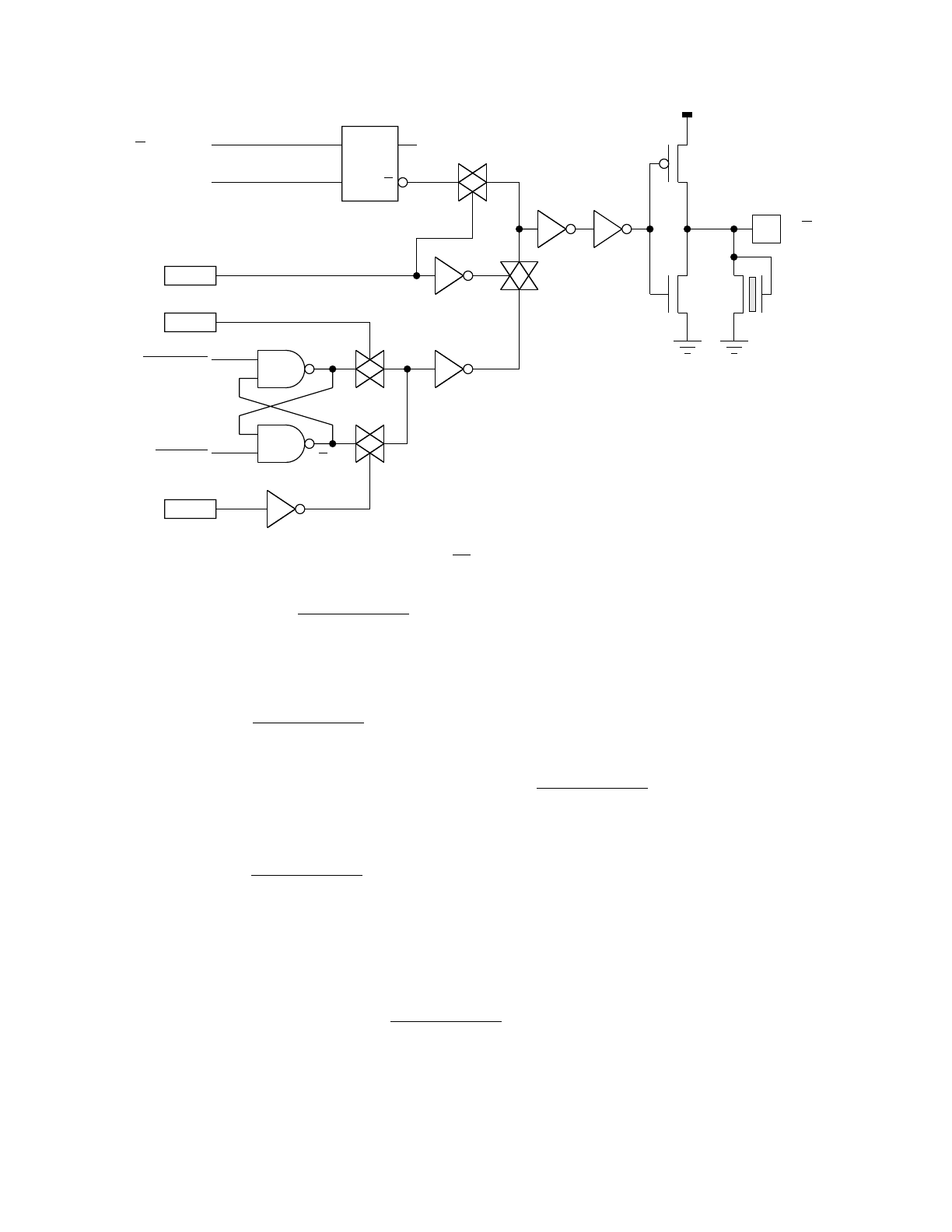
M68HC11 PARALLEL INPUT/OUTPUT MOTOROLA
REFERENCE MANUAL 7-15
Figure 7-10 R/W (STRB) Pin Logic
The start strobe B (STARTSTRB) is an active-low signal from the handshake I/O sub-
system. The conditions that enable strobe B depend on the strobe or handshake mode
in effect. The strobe and handshake modes are controlled by the state of the HNDS
and output/input (OIN) control bits in the PIOC register. When HNDS is zero, the sim-
ple strobe mode is selected, and the state of the OIN control bit is ignored. In simple
strobe mode, STARTSTRB is asserted at the rising edge of the internal PH2 clock fol-
lowing a write to the PORTB register. This time corresponds to the center of the E low
time following the write to port B. When HNDS is one and OIN is zero, full-input hand-
shake is selected. In full-input handshake mode, STARTSTRB is asserted at the rising
edge of the internal PH2 clock following a read of the PORTCL register. This time cor-
responds to the center of the E low time following the read of port C latched data.
When HNDS and OIN are one, full-output handshake is selected. In full-output hand-
shake mode, STARTSTRB is asserted at the rising edge of the internal PH2 clock fol-
lowing a write to the PORTCL register. This time corresponds to the center of the E
low time following the write to port C at PORTCL address.
The end strobe B (ENDSTRB) is an active-low signal from the handshake I/O sub-
system. Three possible conditions can cause the ENDSTRB to be asserted. If the
HNDS bit is zero or if the pulse (PLS) control bit is one, ENDSTRB is asserted exactly
two full E-clock periods after STARTSTRB was asserted. This configuration corre-
sponds to the simple strobe mode or a full-handshake mode where strobe B is config-
ured for pulsed-mode operation. The second condition causing ENDSTRB to be
asserted corresponds to the full-handshake modes where strobe B has been config-
[2]
R/W
(STRB)
VDD
PROTECTION
PIN
N
P
MDA
Q
D
C
Q
HFF
R/W (INTERNAL)
AS
STARTSTRB
ENDSTRB
[3]
[1]
INVB
INVB
Q
Q
[4]
[5]
[6]

MOTOROLA PARALLEL INPUT/OUTPUT M68HC11
7-16 REFERENCE MANUAL
ured for interlocked operation by PLS equal zero. In this case, the ENDSTRB signal is
asserted at the next PH2 rising edge after the selected active edge is detected at the
STRA input pin. The internal PH2 rising edge corresponds to the center of the E low
time. The third condition that can cause ENDSTRB to be asserted is included to avoid
a problem if strobe B is changed from interlocked operation to pulsed operation while
strobe B is active. If PLS is written to one while HNDS is a one, the ENDSTRB signal
is asserted so the strobe B signal will be terminated at the next PH2 rising edge, which
corresponds to the center of the E low time following the cycle where PIOC was written
with HNDS and PLS equal to one.
7.3.3.2 Special Considerations for STRB on MC68HC24 PRU
Because the external PRU does not have access to the internal PH2 clock of the
MC68HC11A8, slight differences exist in the timing of port B, port C, STRA, and STRB
activities. In the MC68HC24, edges on strobe B occur one-quarter E cycle later than
they would in the MC68HC11A8 in single-chip mode. In the case of full-handshake in-
terlocked mode, strobe B will be terminated on the next rising edge of E after a strobe
A edge is detected. The MC68HC24 has a synchronizer on the strobe A input, which
is clocked by AS; thus, the worst-case delay from an edge on strobe A to a response
on strobe B is one and one-eighth E cycles rather than one E cycle (MC68HC11A8).
Because the implementation of the strobe B logic in the MC68HC24 is slightly different
than that in the MC68HC11A8, the third condition that could terminate a strobe B sig-
nal was not included in the MC68HC24. Since changing from interlocked operation to
pulsed operation in the middle of a transaction is not normal, this subtle difference
should not concern most users.
7.3.4 Port C
Port C is the most complex port on the MC68HC11A8 because it can act as general-
purpose bidirectional I/O, full-input or full-output handshake I/O, or as a time-multi-
plexed address/data bus port. Due to the complexity of the port C pin logic, expanded
and single-chip modes of operation will be discussed separately. The following para-
graphs explain the logic associated with port C pins and the idealized timing of select-
ed signals.
Although this section is not specifically concerned with expanded-mode operation of
port C, it is included for reference. A more detailed discussion of the expansion bus is
included in 2.6 Typical Expanded-Mode-System Connections.
7.3.4.1 Port C Pin Logic for Expanded Modes
In expanded modes, port C is a time-multiplexed address/data bus. During the first half
of a cycle, addresses are driven out of port C. During the second half of the cycle, data
is either written out of port C or read into port C. Refer to Figure 7-11 for the following
discussion.
Pin output buffer [1] can be enabled or disabled by the PTCTSC signal. This signal is
driven to zero when address or data information needs to be driven out of port C.
When PTCTSC is one, the output buffer is disabled so port C pins become high-im-
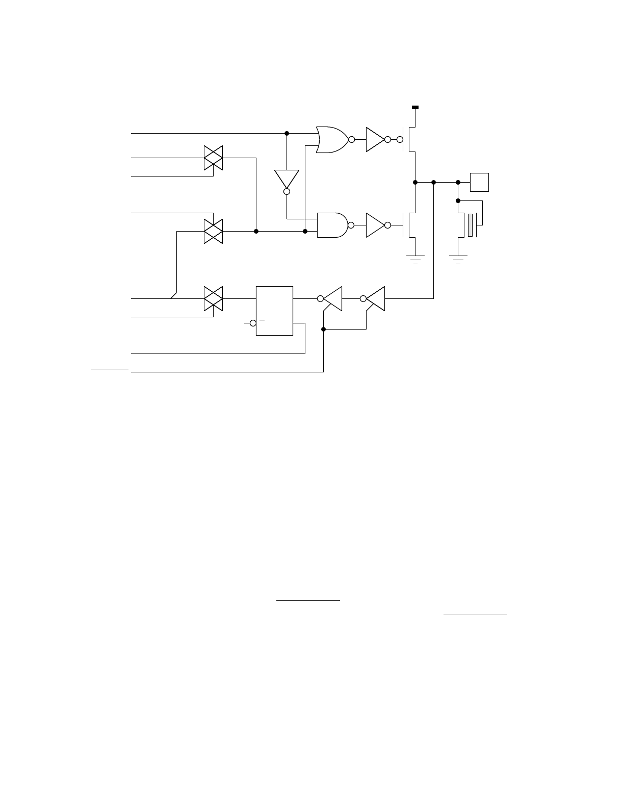
M68HC11 PARALLEL INPUT/OUTPUT MOTOROLA
REFERENCE MANUAL 7-17
pedance input pins (e.g., while data is being read into port C).
Figure 7-11 Port C Expanded Mode Pin Logic
Information to be driven out of port C can come from either transmission gate [2] or [3].
When the address enable (ADDREN) signal is one, transmission gate [2] is enabled
to couple address lines ADDR[7:0] to the output buffer of their associated port C pin.
When the write data enable (WDATEN) signal is one, transmission gate [3] is enabled
to couple data lines DATA[7:0] to the output buffer of their associated port C pin.
In the read direction, data comes from the port C pins to strobe input buffers [6]. Data
from buffers [6] is then clocked into HFF [5] during the E high time. Data is coupled to
the CPU through transmission gate [4] when the read data enable (RDATEN) signal
is one. Since the CPU actually uses the read data during the one-quarter cycle after E
goes low, HFF [5] also provides a level of synchronization for the incoming data.
In normal operation, the stop/wait (STOPWAIT) signal is logic one, which enables buff-
ers [6]. When the MCU is in the stop/wait low-power modes, the STOPWAIT is zero,
and buffers [6] are disabled. While buffers [6] are disabled, intermediate or switching
levels on the port C pins will not cause the relatively high currents normally expected
for CMOS inputs.
7.3.4.2 Summary of Port C Idealized Expanded-Mode Timing
Port C expanded-mode timing includes four types of bus cycles. Write cycles look
PC7–PC0
VDD
PROTECTION
PIN
N
P
Q
D
C
Q
HFF
PTCTSC
A7–A0
WDATEN
STOPWAIT
[5]
[1]
[2]
[4]
[3]
[6]
ADDREN
D7–D0
RDATEN
E

MOTOROLA PARALLEL INPUT/OUTPUT M68HC11
7-18 REFERENCE MANUAL
identical at port C regardless of the address written to. The second type cycle is a read
from an external address. The last two cycle types are reads of internal addresses —
that is, reads of a memory location or register inside the MC68HC11A8. For debug-
ging, the data read from the internal location is driven out of port C to be monitored
with a logic analyzer. For normal use of the MCU, the data from the internal reads is
not driven out of port C because it could conflict with some external device. There is
an internal read visibility (IRV) control bit in the MC68HC11A8 determining whether or
not internal read data will be driven out of port C. The IRV bit and the expansion bus
are described in greater detail in 2.6 Typical Expanded-Mode-System Connec-
tions.
Logic in the MC68HC11A8 generates the signals PTCTSC, ADDREN, WDATEN, and
RDATEN to control the activity of port C, depending on the type bus cycle to be per-
formed. The operation of these signals is explained in 7.3.4.1 Port C Pin Logic for
Expanded Modes.Figure 7-12 summarizes the idealized timing of these signals for
the four types of bus cycles.
7.3.4.3 Port C Single-Chip Mode Pin Logic
Refer to Figure 7-13 for the following discussion. During a write to DDRC, data is
clocked into HFF [1] by the write DDRC (WDDRC) signal. During a read of DDRC,
transmission gate [2] is enabled by the read DDRC (RDDRC) signal, which couples
the output of the DDRC HFF onto the internal data bus. During reset, HFF [1] is forced
to zero, which configures port C pins as high-impedance inputs. The state of DDRC at
the output of HFF [1] controls port C output buffer [3] via NOR gate [4]. The state of
DDRC also influences the source of data for reads of the PORTC register via NAND
gate [6].
The CWOM control bit allows the user to disable the P-channel driver of output buffer
[3]. CWOM simultaneously affects all eight bits of port C. Since the N-channel driver
is not affected by CWOM, CWOM equal one causes port C to become an open-drain-
type output port. When a port C bit is logic zero, it is actively driven low by the N-chan-
nel driver. When a port C bit is logic one, it becomes high impedance since neither the
N- nor P-channel devices are active. It is customary to have an external pull-up resistor
on lines that are driven by open-drain devices. Port C can only be configured for wired-
OR operation when the MCU is in a single-chip mode of operation.
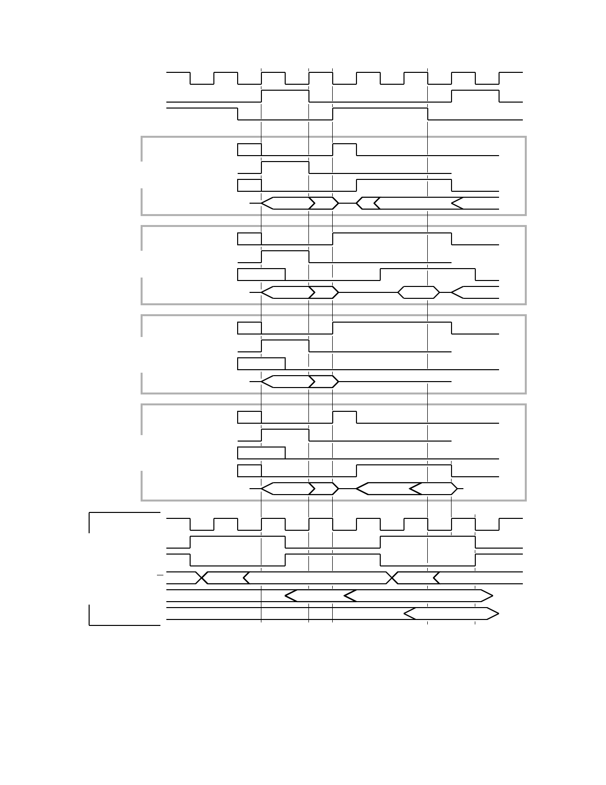
M68HC11 PARALLEL INPUT/OUTPUT MOTOROLA
REFERENCE MANUAL 7-19
Figure 7-12 Summary of Idealized Port C Expanded-Mode Timing
EXTAL
AS
E
INTERNAL SIGNALS
DATA TO CPU
DATA FROM CPU
ADDRESS, R/W
PH2
PH1
OSCCLK
PORT C
WDATEN
RDATEN
ADDREN
PTCTSC
READ FROM
INTERNAL
ADDRESS
(IRV=1)
PORT C
RDATEN
ADDREN
PTCTSC
READ FROM
INTERNAL
ADDRESS
(IRV=0)
PORT C
RDATEN
ADDREN
PTCTSC
READ FROM
EXTERNAL
ADDRESS
PORT C
WDATEN
ADDREN
PTCTSC
WRITE
TO ANY
ADDRESS
ADDR
ADDR
ADDR
ADDR DATA NEXT ADDR
NEXT ADDRDATA
DATA
VALID
VALID
MUST BE VALID
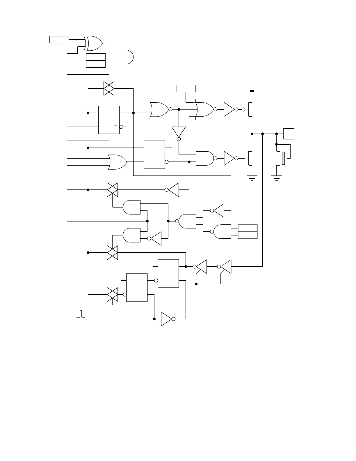
MOTOROLA PARALLEL INPUT/OUTPUT M68HC11
7-20 REFERENCE MANUAL
Figure 7-13 Port C Single-Chip Mode Pin Logic
AND gate [5] provides an override to DDRC during the three-state variation of full-out-
put handshake. In this handshake mode, the HNDS and OIN control bits are ones, en-
abling AND gate [5]. While AND gate [5] is enabled, a one from exclusive-OR gate [7]
will force output buffer [3] to be enabled, regardless of the state of the DDRC bit from
HFF [1]. The EGA control bit specifies the level required at the STRA pin to force port
C pins to be outputs.
CWOM
OIN
HNDS
PC7–PC0
VDD
PROTECTION
PIN
N
P
DQ
HFF
RPORTC
WDDRC
WPORTCL
STOPWAIT
[14]
[3]
[2]
[16]
[13]
RST
D7–D0
RPORTCL
STRAEDGE
Q
D
C
Q
HFF
[15]
[6]
[10]
[8]
D
C
Q
Q
HFF
D
C
Q
Q
HFFR
OIN
HNDS
EGA
WPORTC
RDDRC
STRA PIN
[7]
[5]
[4]
[1]
[12]
[17]
[11]
[9]
[18]
[19]
[20] QC
R

M68HC11 PARALLEL INPUT/OUTPUT MOTOROLA
REFERENCE MANUAL 7-21
While the output-handshake mode is specified, any of the port C bits having their cor-
responding DDRC bits set to zero are configured for the three-state variation of full-
output handshake. For those bits, the corresponding port C pins will appear as high-
impedance inputs while the STRA pin is at its selected inactive level. When the STRA
pin goes to its active level, AND gate [5] will force all port C pins to the output mode.
Any port C bits having their corresponding DDRC bits set to one will be driven outputs,
regardless of the logic at AND gate [5].
While the MCU is operating in output-handshake mode, NAND gate [14] outputs zero
and NAND gate [6] outputs one. When PORTC is read in this case, AND gate [10] en-
ables transmission gate [11] to couple the logic state from point [12] inside the output
buffer onto the internal data bus. When a port C pin is configured for output by its cor-
responding DDRC bit equal one at HFF [1], inverter [15] outputs zero and NAND gate
[6] outputs one. Again, when PORTC is read, AND gate [10] enables transmission
gate [11] to couple the logic state from point [12] inside the output buffer onto the in-
ternal data bus. When neither of the previous conditions are true, the port C pin is con-
figured for input and NAND gate [6] outputs a zero. In this case, when PORTC is read,
AND gate [8] enables transmission gate [9] to couple the buffered state of the corre-
sponding port C pin from the strobed buffers [13] onto the internal data bus.
On writes to port C, data is clocked into the HFF [16] by the output of OR gate [17]. A
write to either the PORTC register or the PORTCL register will enable HFF [16] via OR
gate [17]. The output of HFF [16] drives the port C pins through buffer [3] subject to
the controls on the buffer described in the previous paragraphs.
The port C latch register (PORTCL) is composed of HFFs [18] and [19]. Normally, the
strobe A edge signal (STRAEDGE) is low so HFF [19] is latched and HFF [18] is trans-
parent. When a selected edge is asynchronously detected at the strobe A pin, a short
active-high pulse is issued on STRAEDGE. While STRAEDGE is high, HFF [18] is
temporarily latched so stable data is transferred into HFF [19]. When the PORTCL reg-
ister is read, the RPORTCL signal enables transmission gate [20] to couple the output
of HFF [19] onto the internal data bus.
The STOPWAIT signal is normally high, enabling strobe buffers [13]. When the MCU
is in the stop or wait power-saving modes, STOPWAIT is low, and strobe buffers [13]
are disabled. This function was included to reduce power consumption mainly in the
expanded modes where port C is a multiplexed address/data bus, but there is a side
effect that can influence strobe and handshake input at port C in a very special case.
The wait mode definition states that any enabled interrupt source can be used to force
the MCU to return to normal operation. An active edge at the STRA pin is a possible
source of the interrupt that will wake the MCU from the wait standby mode. Although
the edge at STRA will wake the MCU from the wait mode, valid data will not be latched
into PORTCL because strobe input buffers [13] were disabled at the time of the asyn-
chronous edge at STRA.
7.3.4.4 Port C Idealized Single-Chip Mode Timing
Figure 7-14 shows the idealized timing for important port C control signals. Because
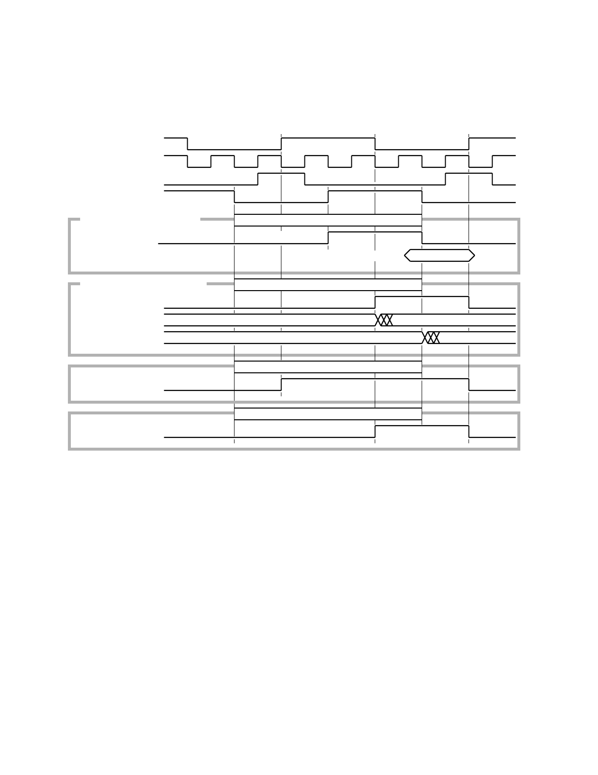
MOTOROLA PARALLEL INPUT/OUTPUT M68HC11
7-22 REFERENCE MANUAL
this timing diagram does not reflect any propagation delays, it cannot be used as a
substitute for data-sheet timing specifications. This information is useful for under-
standing the basis for data-sheet timing specifications so timing information can be ex-
trapolated for bus frequencies other than that used for the data sheet.
Figure 7-14 Idealized Port C Single-Chip Mode Timing
During a read of port C, the RPORTC signal enables transmission gates that drive port
C data onto the internal data bus. After the RPORTC signal is negated, data is held
stable on the self-latching internal data bus. The CPU actually requires data to be sta-
ble for a setup time before and a hold time after the rising edge of the internal PH2
clock. The RPORTC signal is negated one-quarter cycle before this time so data will
be stable while the CPU is actually reading it.
During a DDRC read, the RDDRC signal enables a transmission gate to couple the
state of the DDRC bit to the internal data bus. In contrast to the RPORTC signal, RD-
DRC is active while the CPU is actually reading the data from the internal data bus,
which does not pose potential problems because it is not possible for the DDRC value
to change in the same cycle it is being read.
The timing for the RPORTCL signal is the same as that for the RDDRC signal. Unlike
PORT C OUTPUT (SINGLE-CHIP MODE)
NEW PORT C DATA
VALID DATA REQUIRED AT CPU
WRITE TO PORT C
READ FROM PORT C
PH2 (INTERNAL)
EXTAL
AS
RPORTC
WPORTC OR WPORTCL
PORT C OUTPUT PINS
E
NEW PORT C DATA
PORT C OUTPUT PINS
(MC68HC24 ONLY)
RPORTCL OR RDDRC
READ PORTCL OR DDRC
WDDRC
WRITE TO DDRC
PORT C INPUT (SINGLE-CHIP MODE)

M68HC11 PARALLEL INPUT/OUTPUT MOTOROLA
REFERENCE MANUAL 7-23
DDRC data, data in the PORTCL register can change at any time since the strobe A
latching edge is asynchronous. Since it is undesirable for data to be changing at the
instant the CPU is latching in this data, the user should avoid this synchronization haz-
ard. Usually, the system design automatically solves the problem because an edge on
STRA cannot normally occur during a read of PORTCL. For example, in a full-input
handshake, PORTCL is only read in response to recognizing that the STAF has been
set. In such a case, the edge that caused STAF to be set and data to be latched into
PORTCL will have occurred several cycles before the PORTCL read could possibly
occur. Also, in the full-handshake protocol, the external device is inhibited from latch-
ing new data into PORTCL until the previous data is read from PORTCL. This inhibit
is accomplished by the STRB handshake output.
Writes to port C at PORTC or PORTCL and writes to DDRC are controlled by
WPORTC, WPORTCL, and WDDRC, respectively. All three signals are synchronized
to the falling edge of the internal PH2 clock, which corresponds to the center of the E
high time.
7.3.4.5 Special Considerations for Port C on MC68HC24 PRU
Since the external PRU does not have access to the internal PH2 clock of the
MC68HC11A8, there are slight differences in the timing of port B, port C, STRA, and
STRB activities. Figure 7-14 shows the differences between internal MC68HC11A8
writes to port C and MC68HC24 writes to port C.
7.3.5 AS (STRA) Pin
In expanded modes, this pin acts as the AS control signal, which is used to demultiplex
low-order addresses from data at port C. In single-chip modes, this pin acts as the
STRA input, which serves the handshake I/O subsystem on the MC68HC11A8. The
MC68HC24 can be used to regain the STRA functions when the MCU is operating in
an expanded mode.
7.3.5.1 AS (STRA) Pin Logic
Refer to Figure 7-15 for the following discussion. When the MC68HC11A8 is operat-
ing in a single-chip mode, the MDA control bit is zero; thus, both the P- and N-channel
output drivers are disabled. While the MCU is operating in an expanded mode, the
MDA control bit enables the output driver logic. As long as the MCU is not in stop
mode, the AS signal is buffered and driven out the AS pin.
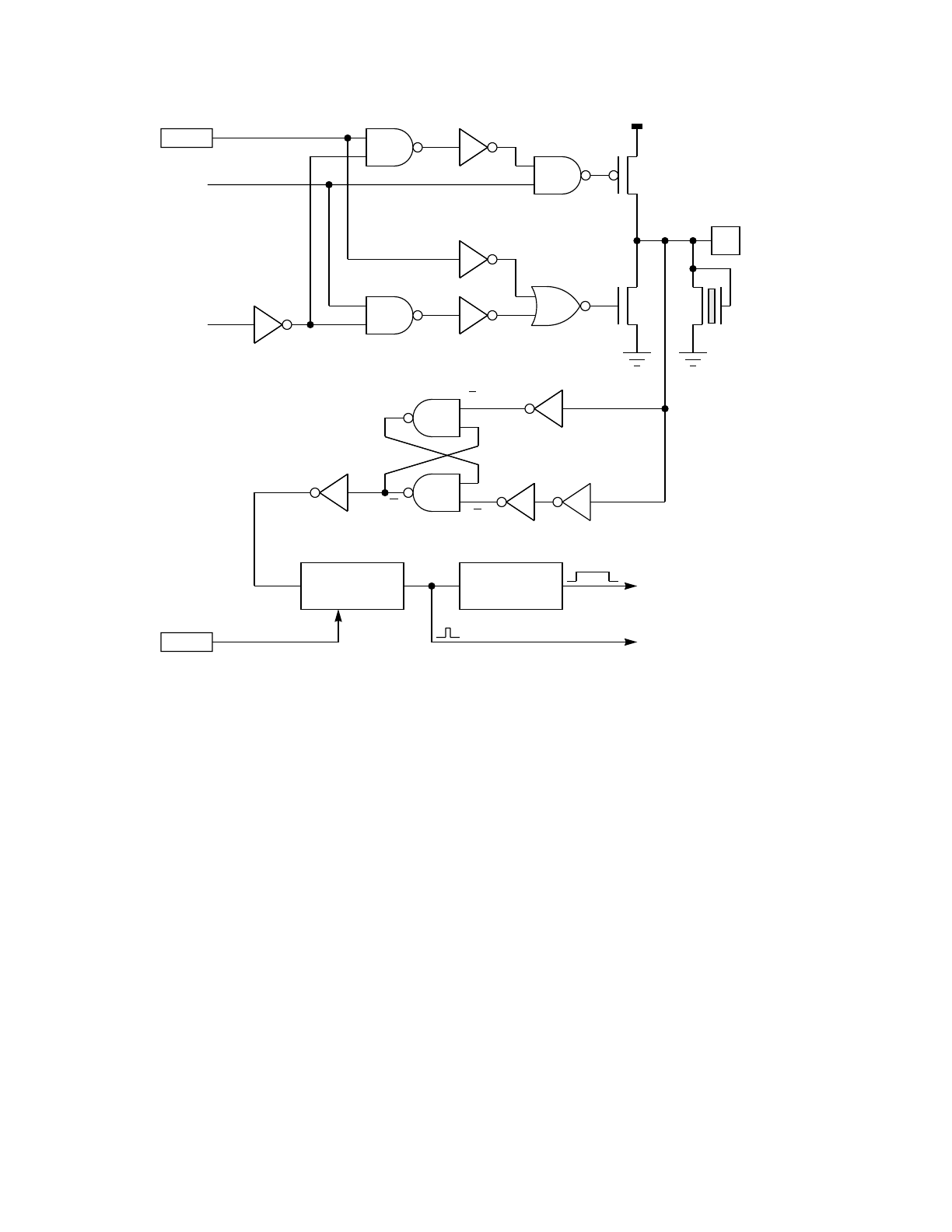
MOTOROLA PARALLEL INPUT/OUTPUT M68HC11
7-24 REFERENCE MANUAL
Figure 7-15 AS (STRA) Pin Logic
When the MC68HC11A8 is in stop mode, the STOP signal goes high, which forces the
AS pin to logic zero. A one on STOP forces a zero on one input of NAND gate [1],
which forces a zero on one input of NAND gate [2], which disables the P-channel driv-
er. The one on STOP also forces a one at the output of NAND gate [3], which places
a zero on the lower input of NOR gate [4]. Since the one on MDA forces the other input
of NOR gate [4] to zero, the output of this NOR gate will be one, which enables the N-
channel driver and forces the pin to zero.
Hysteresis buffer [5] is described in 7.3.1.1 PA[2:0] (IC[3:1]) Pin Logic. EGA controls
the block of logic [7], which detects asynchronous edges on the signal from inverter
[6], the buffered signal from the strobe A pin. The output from the block of logic [7] is
a short high-going asynchronous pulse, which is used to asynchronously latch data
from the port C pins into the PORTCL register.
In response to the asynchronous pulse from block [7], the block of logic [8] produces
a pulse that is synchronized to the internal PH2 clock. Provided the asynchronous
pulse meets a setup time before the rising edge of PH2, the output of block [8] will go
SYNCHRONIZE
TO PH2
USED TO SET STAF FLAG
AND TO TERMINATE STRB
Q
[5]
STOP
AS
MDA
[1]
EGA
DETECT
ACTIVE EDGE
ON STRA
SHORT ASYNCHRONOUS
PULSE USED TO TRIGGER
PORTCL LATCHES
[3]
[6]
[7] [8]
AS
(STRA)
VDD
PROTECTION
PIN
N
P
[2]
[4]
QR
S

M68HC11 PARALLEL INPUT/OUTPUT MOTOROLA
REFERENCE MANUAL 7-25
high at that PH2 rising edge and stay high until PH2 goes low. If the setup time is not
met, the pulse will appear at the next PH2, causing a delay from when an edge is pre-
sented at the STRA pin until it is recognized by the logic of block [8]. The delay could
be from a few nanoseconds to a full E-clock cycle, depending on where the edge oc-
curs relative to the clocks. The rising edge of the internal PH2 clock corresponds to
the center of the E-clock low time. A significant number of internal logic-gate delays
exists between the STRA pin and the block of logic [8].
The synchronized pulse from block [8] is used for several functions in the handshake
I/O subsystem. STAF is set by this pulse. The arming mechanism for automatically
clearing STAF is cleared by this pulse. This pulse can terminate the STRB output in
some handshake modes. These functions and their timing are discussed in greater de-
tail in 7.4 Handshake I/O Subsystem.
7.3.5.2 Special Considerations for STRA on MC68HC24 PRU
Because the external PRU does not have access to the internal PH2 clock of the
MC68HC11A8, slight differences exist in the timing of port B, port C, STRA, and STRB
activities. The differences for strobe A are associated with the block of logic [8] in Fig-
ure 7-15. Although Figure 7-15 depicts the MC68HC11A8, there is a similar block of
logic in the MC68HC24. In the MC68HC24, AS and E are used to synchronize the
strobe A pulse to the E clock. Any strobe A edge meeting a setup time to the falling
edge of AS results in a synchronized pulse that is high for the next E-clock high time.
This pulse is used for the same purposes as the PH2 synchronized pulse in the
MC68HC11A8.
7.3.6 Port D
Port D is a six-bit bidirectional data port. Two port D pins alternately serve as the re-
ceive and transmit data pins for the on-chip asynchronous SCI system. The other four
port D pins alternately serve the on-chip synchronous SPI system. Although the pin
logic for all six port D pins is essentially identical, each pin is described separately to
note subtle differences. The following paragraphs explain the detailed logic associated
with port D pins and the idealized timing of important port D control signals.
7.3.6.1 PD0 (RxD) Pin Logic
Refer to Figure 7-16 for the following discussion. The data direction specification for
this pin is held in HFF [1]. During a write to the DDRD register, the WDDRD signal is
asserted, which causes data to be transferred into HFF [1] from the internal data bus.
A read of DDRD causes the RDDRD signal to be asserted, which enables transmis-
sion gate [2] to couple the output of HFF [1] onto the internal data bus. During reset,
HFF [1] is cleared to zero, configuring this pin as a high-impedance input.
The state of DDRD controls the pin output buffer via AND gate [3], and DDRD affects
the source of data for port D reads via transmission gates [4] and [5]. When the DDRD
bit from HFF [1] is zero, AND gate [3] outputs a zero, which disables output driver [9].
When the DDRD bit from HFF [1] is zero, transmission gate [5] is enabled. In this case,
reads of port D enable transmission gate [6], coupling the buffered pin state from in-
verters [7] to the internal data bus. When the DDRD bit from HFF [1] is one, transmis-
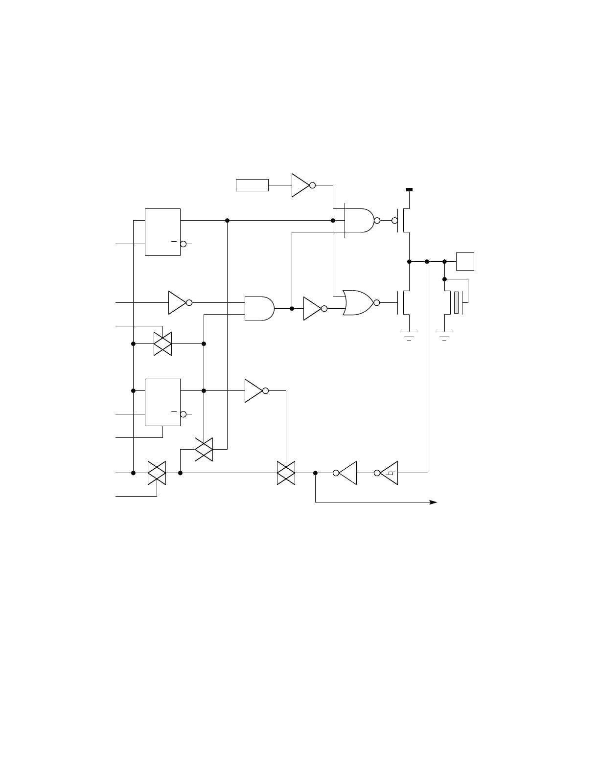
MOTOROLA PARALLEL INPUT/OUTPUT M68HC11
7-26 REFERENCE MANUAL
sion gate [4] is enabled. In this case, reads of port D enable transmission gate [6],
coupling the level from the output of HFF [8] to the internal data bus, which corre-
sponds to the output level for the pin before output driver [9]. Since output driver [9]
can be configured for wired-OR operation, some external source can force the pin low,
even if the logic for this pin is trying to output a one. In this case, a read of port D will
return the intended logic one from inside the output buffer rather than the zero from
the pin.
Figure 7-16 PD0 (RxD) Pin Logic
During a write to port D, the WPORTD signal is asserted, causing data from the inter-
nal data bus to be latched into HFF [8]. Written data is then buffered to the pin by out-
put driver [9] subject to data direction control from AND gate [3] and wired-OR control
from the DWOM control bit. When the DWOM control bit is one, the P-channel driver
is disabled so port D outputs act as open-drain drivers. The DWOM control bit simul-
taneously affects all port D pins.
When the output of AND gate [3] is zero, the output driver is completely disabled; thus,
this pin is configured as a high-impedance input. AND gate [3] will output a zero to dis-
able the output driver whenever the corresponding DDRD bit is zero from HFF [1].
HFF
D
C
Q
R
PD0
(RxD)
VDD
PROTECTION
PIN
N
P
[9]
[1]
DWOM
HFFR
D
C
Q
TO SCI RECEIVER
RDDRD
RCVON
WPORTD
D0
RST
WDDRD
RPORTD
[2]
[4]
[5] [7]
[6]
[3]
[8]
Q
Q

M68HC11 PARALLEL INPUT/OUTPUT MOTOROLA
REFERENCE MANUAL 7-27
AND gate [3] will also disable the output driver when the SCI receiver is enabled by
the receiver-on signal (RCVON). The state of the DDRD bit still influences the source
of read data when the RCVON signal is forcing the pin to a high-impedance state.
This pin alternately serves as the receive data (RxD) input pin for the asynchronous
SCI system. The SCI receiver is enabled by the receive enable (RE) control bit in an
SCI control register, which forces the RCVON signal to one, disabling pin output driver
[9], regardless of the state of the DDRD bit from HFF [1]. The state of the DDRD bit
allows the programmer to read the RxD pin (DDRD = 0) or the value in port D latch [8]
(when DDRD = 1). Data from the pin is buffered by inverters [7] and driven to the SCI
receive logic. The data path from the pin to the SCI receive logic is not affected by the
state of DDRD.
7.3.6.2 PD1 (TxD) Pin Logic
Refer to Figure 7-17 for the following discussion. The data direction specification for
this pin is held in HFF [1]. During a write to the DDRD register, the WDDRD signal is
asserted, causing data to be transferred into HFF [1] from the internal data bus. A read
of DDRD causes the RDDRD signal to be asserted, which enables transmission gate
[2] to couple the output of HFF [1] onto the internal data bus. During reset, HFF [1] is
cleared to zero, which configures this pin as a high-impedance input.
The state of DDRD controls the pin output buffer via OR gate [3], and DDRD affects
the source of data for port D reads via transmission gates [4] and [5]. When the DDRD
bit from HFF [1] is one, OR gate [3] outputs a one, which enables output driver [9]. Al-
so, when the DDRD bit from HFF [1] is one, transmission gate [4] is enabled. In this
case, reads of port D enable transmission gate [6], which couples the level from the
output of HFF [8] to the internal data bus. The value returned on such a read corre-
sponds to the last value written to the corresponding bit of port D. Since output driver
[9] can be configured for wired-OR operation, some external source can force the pin
low even if the pin logic for this pin is attempting to output a one. If the DDRD bit did
not affect the source of the read data, an erroneous zero could be read when the pin
logic is actually trying to output a one. When the DDRD bit from HFF [1] is zero, OR
gate [3] outputs a zero, which disables output driver [9]. Also, when the DDRD bit is
zero, transmission gate [5] is enabled. In this case, reads of port D enable transmis-
sion gate [6], which couples the buffered pin state from inverters [7] to the internal data
bus.
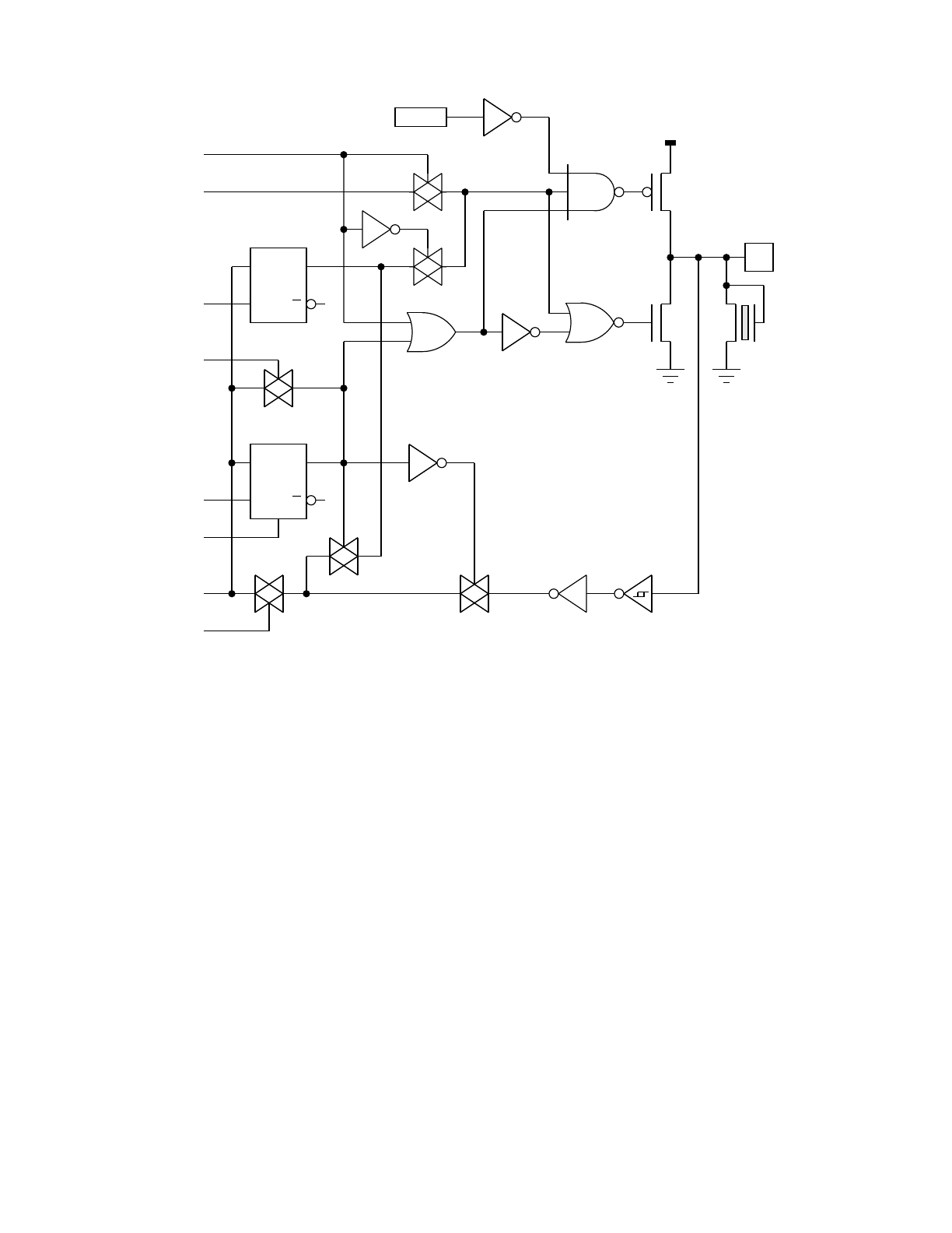
MOTOROLA PARALLEL INPUT/OUTPUT M68HC11
7-28 REFERENCE MANUAL
Figure 7-17 PD1 (TxD) Pin Logic
During a write to port D, the WPORTD signal is asserted, causing data from the inter-
nal data bus to be latched into HFF [8]. When the SCI transmitter is enabled, the trans-
mit-on (XMITON) signal is one and transmission gate [10] is enabled, which couples
serial transmit data (XMITDATA) to pin driver [9]. When the SCI transmitter is disabled,
the XMITON signal is zero, and transmission gate [11] is enabled, which couples port
D data from HFF [8] to pin driver [9]. Pin output driver [9] is enabled by data direction
logic from OR gate [3]. The DWOM control bit can optionally disable the P-channel
driver of output buffer [9].
When the DWOM control bit is one, the P-channel driver is disabled, causing port D
outputs to act as open-drain drivers. The DWOM control bit concurrently affects all port
D pins. When the output of OR gate [3] is zero, the output driver is completely disabled;
thus, this pin is configured as a high-impedance input. OR gate [3] will output a zero
to disable the output driver whenever the corresponding DDRD bit is zero from HFF
[1] and the SCI transmitter is disabled by the XMITON signal. The state of the DDRD
bit still influences the source of read data when the XMITON signal is forcing the pin
to the output configuration.
HFF
D
C
Q
R
PD1
(TxD)
VDD
PROTECTION
PIN
N
P
[9]
[1]
DWOM
HFFR
D
C
Q
RDDRD
WPORTD
D1
RST
WDDRD
RPORTD
[2]
[4]
[5] [7]
[6]
[3]
[8]
XMITON
XMITDATA
[10]
[11]
Q
Q

M68HC11 PARALLEL INPUT/OUTPUT MOTOROLA
REFERENCE MANUAL 7-29
This pin alternately serves as the transmit data (TxD) output pin for the asynchronous
SCI system. The SCI transmitter is enabled by the TE control bit in an SCI control reg-
ister. Enabling the transmitter forces the pin driver to be configured as an output by
forcing a one at the output of OR gate [3]. The state of the DDRD bit allows the pro-
grammer to read the TxD pin (DDRD = 0) or the value in port D latch [8] (when DDRD
equals one). The SCI transmitter retains control of the port D pin by keeping XMITON
equal to one as long as any information is being transmitted (even after the TE bit is
written to zero). This control assures that a transmission will not be cut off in the middle
of a serial character.
The user can control what happens to the TxD pin when the transmitter is finished.
When the transmitter is finished using the TxD pin, the XMITON signal switches from
one to zero, which causes the data direction to be controlled by the DDRD bit from
HFF [1] instead of the XMITON input to OR gate [3]. Disabling XMITON also causes
transmission gate [10] to be disabled and transmission gate [11] to be enabled. If the
corresponding DDRD bit is zero, the pin will revert to being a high-impedance input
when the transmitter is finished. If the DDRD bit is one and the last data written to the
corresponding bit of port D was a zero, the pin will revert to a driven logic zero when
the transmitter is finished. If the DDRD bit is one and the last data written to the corre-
sponding bit of port D was a one, the pin will revert to a driven logic one when the trans-
mitter is finished.
7.3.6.3 PD2 (MISO) Pin Logic
This pin alternately functions as the MISO pin when the synchronous SPI system is
enabled. Refer to Figure 7-18 for the following discussion. The data direction specifi-
cation for this pin is held in HFF [1], During a write to the DDRD register, the WDDRD
signal is asserted, which causes data to be transferred into HFF [1] from the internal
data bus. A read of DDRD causes the RDDRD signal to be asserted, enabling trans-
mission gate [2] to couple the output of HFF [1] onto the internal data bus.
When HFF [1] is cleared to zero, this pin is configured as a high-impedance input. OR
gate [13] causes HFF [1] to be cleared to zero during reset. OR gate [13] also causes
HFF [1] to be cleared if an SPI mode fault (MFAULT) occurs. An SPI mode fault is
caused when a device configured as a master SPI device is selected as if it were a
slave. This condition could indicate that more than one SPI device is attempting to
drive the common SPI lines, which could cause a bus conflict. To avoid the possibility
of latchup, the port D pins associated with the SPI are immediately forced to their input
configuration.
The actual data direction for this port D pin is determined by the logic output of NAND
gate [3]. When the SPI system is disabled, the DDRD bit from HFF [1] controls direc-
tion. When the SPI system is enabled in master mode, this pin is forced to a high-im-
pedance input. When the SPI system is enabled in slave mode, the DDRD bit from
HFF [1] controls direction. This last condition means that the user must set the corre-
sponding DDRD bit to one to enable slave data output from this pin when the SPI sys-
tem is enabled for slave operation. The uses and implications of this logic are
discussed in greater detail in SECTION 8 SYNCHRONOUS SERIAL PERIPHERAL
INTERFACE.
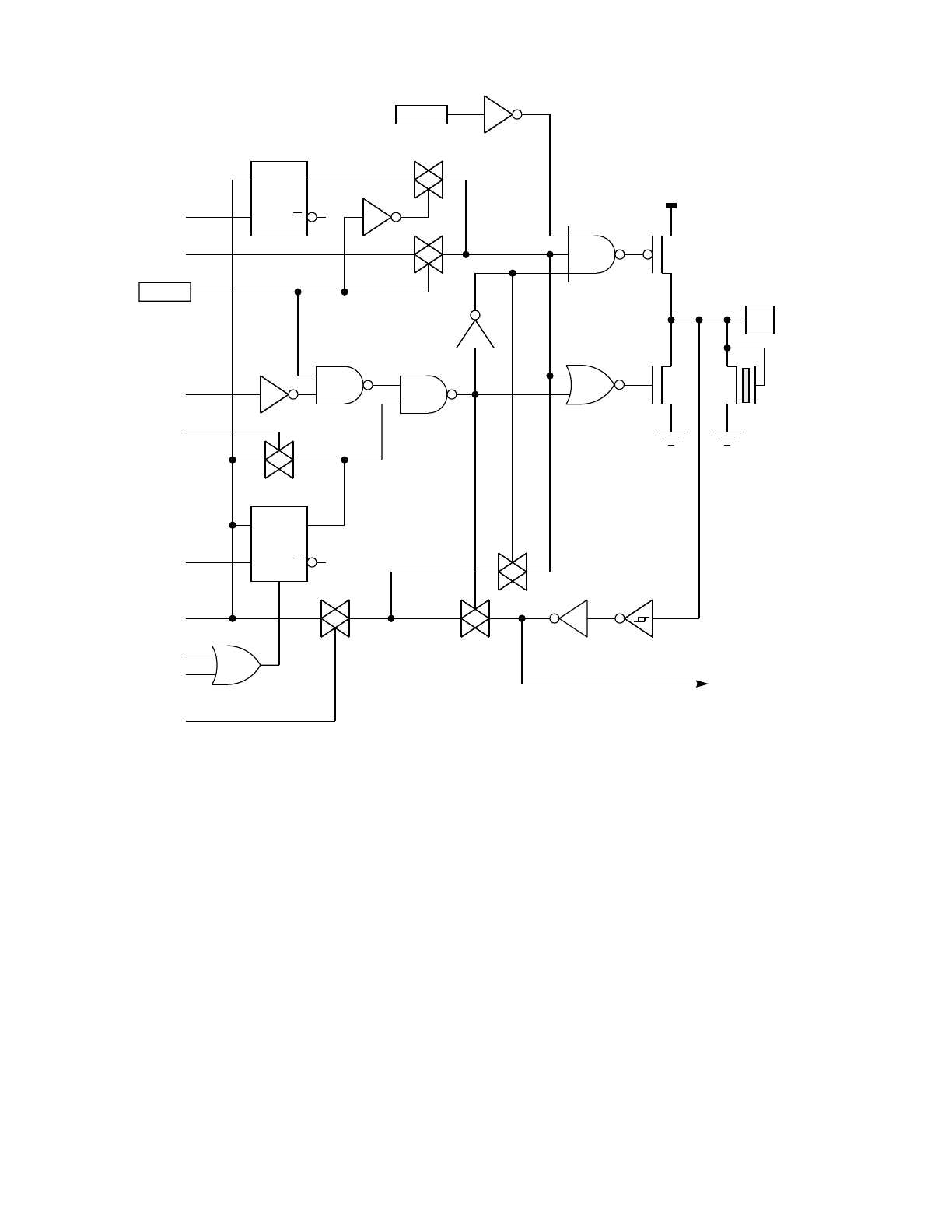
MOTOROLA PARALLEL INPUT/OUTPUT M68HC11
7-30 REFERENCE MANUAL
Figure 7-18 PD2 (MISO) Pin Logic
When the output of NAND gate [3] is one, driver [9] is disabled so the pin is configured
as a high-impedance input. To enable pin driver [9], both inputs to NAND gate [3] must
be ones. When the SPI system is disabled, SPE is zero, which makes the output of
NAND gate [12] a one. A logic one enables NAND gate [3] so that the DDRD bit from
HFF [1] can enable or disable driver [9]. When the SPI system is operating as a mas-
ter, SPE will be one and slave on (SLAVON) will be zero. This configuration causes
NAND gate [12] to output a zero, which disables output driver [9], regardless of the
state of the DDRD bit at HFF [1]. When the SPI system is enabled as a slave, SPE is
one and SLAVON is one. This configuration causes NAND gate [12] to output a one,
which enables NAND gate [3] to control the direction of output buffer [9] based on the
state of the DDRD bit from HFF [1].
Output driver [9] can be placed in a wired-OR configuration by the DWOM control bit.
This control bit simultaneously affects all six port D pins. When DWOM is one, the P-
HFF
D
C
Q
R
PD2
(MISO)
VDD
PROTECTION
PIN
N
P
[9]
[1]
DWOM
HFFR
D
C
Q
RDDRD
WPORTD
D2
MFAULT
WDDRD
RPORTD
[2]
[4]
[5] [7]
[6]
[3]
[8]
[10]
[11]
SLAVDO
SPE
RST
SLAVON
[12]
[13] TO SPI
MASTER DATA IN
Q
Q

M68HC11 PARALLEL INPUT/OUTPUT MOTOROLA
REFERENCE MANUAL 7-31
channel device in the output driver is disabled so the pin cannot be actively driven
high. When the pin attempts to output a logic one, the N-channel device is disabled;
thus, the pin appears as a high-impedance input. An external pull-up is used to pas-
sively pull the pin high.
The data for output driver [9] comes from transmission gate [10] or [11]. When the SPI
system is enabled, the SPE bit is one; thus, transmission gate [10] is enabled, and
data for the output driver comes from the SPI slave data output signal (SLAVDO).
When the SPI system is disabled, the SPE control bit is zero; thus, transmission gate
[10] is disabled and transmission gate [11] is enabled. In this case, port D data is cou-
pled from the output of HFF [8] to the input of output driver [9]. During a write to port
D, the WPORTD signal is asserted, which causes data to be latched into HFF [8] from
the internal data bus.
During a read of port D, transmission gate [6] is enabled by the RPORTD signal to cou-
ple data to the internal data bus. The source of data for port D reads depends on the
direction control for the output driver. If the output of NAND gate [3] is zero, output driv-
er [9] is enabled and transmission gate [4] is enabled. In this case, port D reads return
the data from a point inside the output driver. If the output of NAND gate [3] is one,
transmission gate [5] is enabled. In this case, reads of port D return the buffered state
from the pin through inverters [7].
The output of inverters [7] drives the serial master data input to the SPI system logic.
The source of this data is always from the MISO pin and is not affected by the data
direction logic.
7.3.6.4 PD3 (MOSI) Pin Logic
This pin alternately functions as the MOSI pin when the synchronous SPI system is
enabled. Refer to Figure 7-19 for the following discussion. The data direction specifi-
cation for this pin is held in HFF [1]. During a write to the DDRD register, the WDDRD
signal is asserted, causing data to be transferred into HFF [1] from the internal data
bus. A read of DDRD causes the RDDRD signal to be asserted, which enables trans-
mission gate [2] to couple the output of HFF [1] onto the internal data bus.
When HFF [1] is cleared to zero, this pin is configured as a high-impedance input. OR
gate [13] causes HFF [1] to be cleared to zero during reset. OR gate [13] also causes
HFF [1] to be cleared if an SPI mode fault occurs. An SPI mode fault is caused when
a device configured as a master SPI is selected as if it were a slave. This condition
could indicate that more than one SPI device is attempting to drive the common SPI
lines, which could cause a bus conflict. To avoid the possibility of latchup, the port D
pins associated with the SPI are immediately forced to their input configuration.
The actual data direction for this port D pin is determined by the logic output of NAND
gate [3]. When the SPI system is disabled, the DDRD bit from HFF [1] controls direc-
tion. When the SPI system is enabled in slave mode, this pin is configured as a high-
impedance input. When the SPI system is enabled in master mode, the DDRD bit from
HFF [1] controls direction. This last condition means that the user must set the corre-
sponding DDRD bit to one to enable master data output from this pin when the SPI
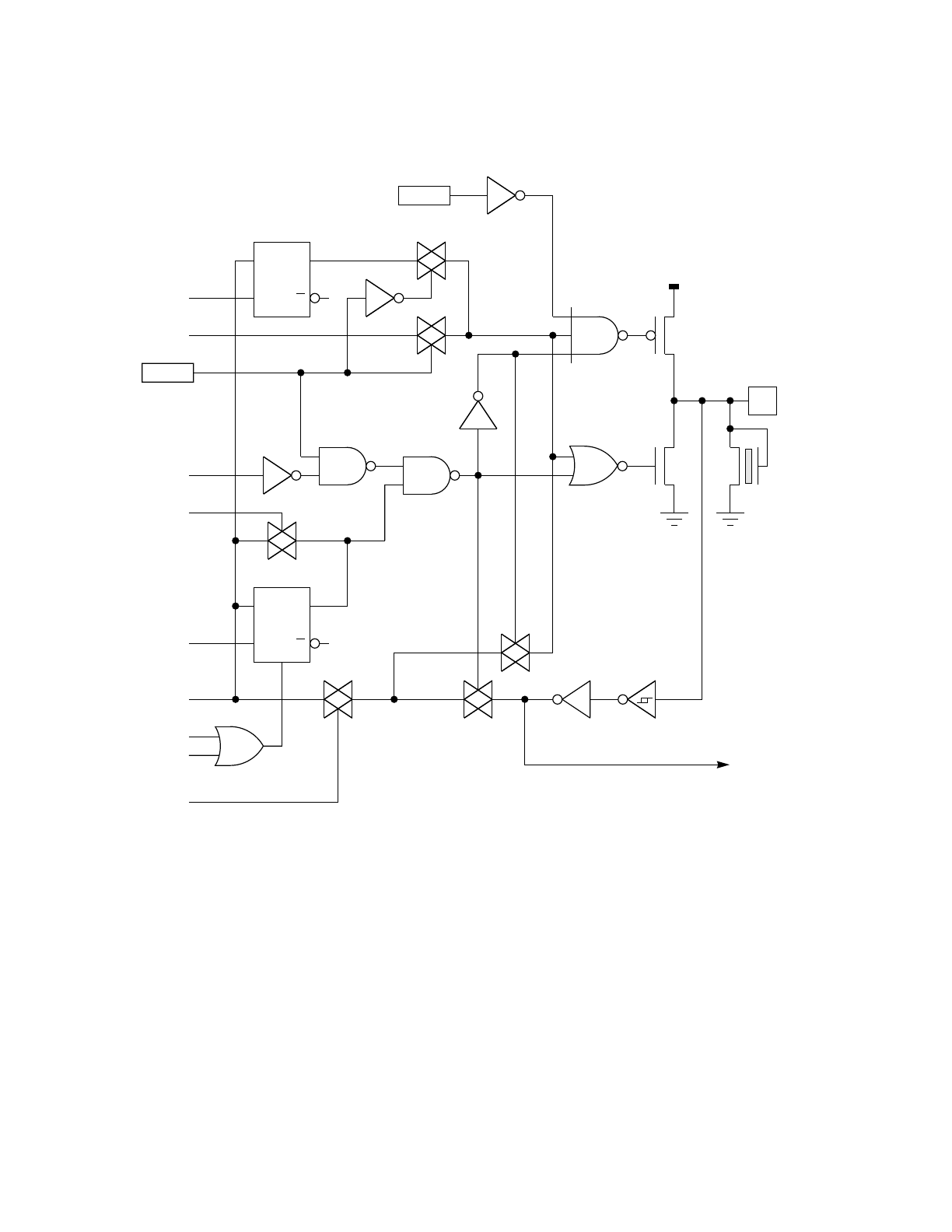
MOTOROLA PARALLEL INPUT/OUTPUT M68HC11
7-32 REFERENCE MANUAL
system is configured for master operation. The uses and implications of this logic are
discussed in greater detail in SECTION 8 SYNCHRONOUS SERIAL PERIPHERAL
INTERFACE.
Figure 7-19 PD3 (MOSI) Pin Logic
When the output of NAND gate [3] is one, driver [9] is disabled; thus, the pin is config-
ured as a high-impedance input. To enable pin driver [9], both inputs to NAND gate [3]
must be ones. When the SPI system is disabled, SPE is zero, making the output of
NAND gate [12] a one. This configuration enables NAND gate [3] so that the DDRD
bit from HFF [1] can enable or disable driver [9]. When the SPI system is enabled as
a slave, SPE is one and master on (MSTRON) is zero. This configuration causes
NAND gate [12] to output zero, which disables output driver [9], regardless of the state
of the DDRD bit at HFF [1]. When the SPI system is enabled as a master, SPE is one
and MSTRON is one. This configuration causes NAND gate [12] to output a one, which
enables NAND gate [3] to control the direction of output buffer [9] based on the state
HFF
D
C
Q
R
PD3
(MOSI)
VDD
PROTECTION
PIN
N
P
[9]
[1]
DWOM
HFFR
D
C
Q
RDDRD
WPORTD
D3
MFAULT
WDDRD
RPORTD
[2]
[4]
[5] [7]
[6]
[3]
[8]
[10]
[11]
MSTRDO
SPE
RST
MSTRON
[12]
[13] TO SPI
SLAVE DATA IN
Q
Q

M68HC11 PARALLEL INPUT/OUTPUT MOTOROLA
REFERENCE MANUAL 7-33
of the DDRD bit from HFF [1].
Output driver [9] can be placed in a wired-OR configuration by the DWOM control bit.
This control bit simultaneously affects all six port D pins. When DWOM is one, the P-
channel device in the output driver is disabled so the pin cannot be actively driven
high. When the pin attempts to output logic one, the N-channel device is disabled;
thus, the pin appears as high-impedance input. An external pull-up is used to passively
pull the pin high.
The data for output driver [9] comes from transmission gate [10] or [11]. When the SPI
system is enabled, the SPE bit is one; transmission gate [10] is enabled, and data for
the output driver comes from the SPI master data output signal (MSTRDO). When the
SPI system is disabled, the SPE control bit is zero; transmission gate [10] is disabled
and transmission gate [11] is enabled. In this case, port D data is coupled from the out-
put of HFF [8] to the input of output driver [9]. During a write to port D, the WPORTD
signal is asserted, which causes data to be latched into HFF [8] from the internal data
bus.
During a read of port D, transmission gate [6] is enabled by the RPORTD signal to cou-
ple data to the internal data bus. The source of data for port D reads depends on the
direction control for the output driver. If the output of NAND gate [3] is zero, output driv-
er [9] is enabled and transmission gate [4] is enabled. In this case, port D reads return
the data from a point inside the output driver. If the output of NAND gate [3] is one,
transmission gate [5] is enabled. In this case, reads of port D return the buffered state
from the pin through inverters [7].
The output of inverters [7] drives the serial slave data input to the SPI system logic.
Because the source of this data is always from the MOSI pin, it is not affected by the
data direction logic.
7.3.6.5 PD4 (SCK) Pin Logic
This pin alternately functions as the SPI SCK output pin when the synchronous SPI
system is enabled. Refer to Figure 7-20 for the following discussion. The data direc-
tion specification for this pin is held in HFF [1]. During a write to the DDRD register,
the WDDRD signal is asserted, causing data to be transferred into HFF [1] from the
internal data bus. A read of DDRD causes the RDDRD signal to be asserted, which
enables transmission gate [2] to couple the output of HFF [1] onto the internal data
bus.
When HFF [1] is cleared to zero, this pin is configured as a high-impedance input. OR
gate [13] causes HFF [1] to be cleared to zero during reset. OR gate [13] also causes
HFF [1] to be cleared if there is an SPI mode fault. An SPI mode fault is caused when
a device configured as a master SPI device is selected as if it were a slave. This con-
dition could indicate that more than one SPI device is attempting to drive the common
SPI lines, which could cause a bus conflict. To avoid the possibility of latchup, the port
D pins associated with the SPI are immediately forced to their input configuration.
The actual data direction for this port D pin is determined by the logic output of NAND
gate [3]. When the SPI system is disabled, the DDRD bit from HFF [1] controls direc-
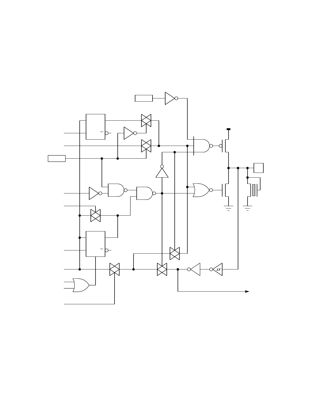
MOTOROLA PARALLEL INPUT/OUTPUT M68HC11
7-34 REFERENCE MANUAL
tion. When the SPI system is enabled in slave mode, this pin is forced to a high-im-
pedance input. When the SPI system is enabled in master mode, the DDRD bit from
HFF [1] controls direction. This last condition means that the user must set the corre-
sponding DDRD bit to one to enable the master clock output from this pin when the
SPI system is configured for master operation. The uses and implications of this logic
are discussed in greater detail in SECTION 8 SYNCHRONOUS SERIAL PERIPHER-
AL INTERFACE.
Figure 7-20 PD4 (SCK) Pin Logic
When the output of NAND gate [3] is one, driver [9] is disabled so the pin is configured
as a high-impedance input. To enable pin driver [9], both inputs to NAND gate [3] must
be ones. When the SPI system is disabled, SPE is zero, which makes the output of
NAND gate [12] a one. This enables NAND gate [3] so that the DDRD bit from HFF [1]
can enable or disable driver [9]. When the SPI system is enabled as a slave, SPE is
HFF
D
C
Q
R
PD4
(SCK)
VDD
PROTECTION
PIN
N
P
[9]
[1]
DWOM
HFFR
D
C
Q
RDDRD
WPORTD
D4
MFAULT
WDDRD
RPORTD
[2]
[4]
[5] [7]
[6]
[3]
[8]
[10]
[11]
SPISCK
SPE
RST
MSTRON
[12]
[13] TO SPI
SLAVE CLOCK
Q
Q

M68HC11 PARALLEL INPUT/OUTPUT MOTOROLA
REFERENCE MANUAL 7-35
one and MSTRON is zero. This configuration causes NAND gate [12] to output a zero,
which disables output driver [9], regardless of the state of the DDRD bit at HFF [1].
When the SPI system is enabled as a master, SPE is one and MSTRON is one. This
configuration causes NAND gate [12] to output a one, which enables NAND gate [3]
to control the direction of output buffer [9] based on the state of the DDRD bit from HFF
[1].
Output driver [9] can be placed in a wired-OR configuration by the DWOM control bit.
This control bit simultaneously affects all six port D pins. When DWOM is one, the P-
channel device in the output driver is disabled so the pin cannot be actively driven
high. When the pin attempts to output a logic one, the N-channel device is off; thus,
the pin appears as a high-impedance input. An external pull-up is used to passively
pull the pin high.
The data for output driver [9] comes from transmission gate [10] or [11]. When the SPI
system is enabled, the SPE bit is one; thus, transmission gate [10] is enabled, and
data for the output driver comes from the SPI master clock output signal (SPISCK).
When the SPI system is disabled, the SPE control bit is zero; transmission gate [10]
is disabled and transmission gate [11] is enabled. In this case, port D data is coupled
from the output of HFF [8] to the input of output driver [9]. During a write to port D, the
WPORTD signal is asserted, which causes data to be latched into HFF [8] from the
internal data bus.
During a read of port D, transmission gate [6] is enabled by the RPORTD signal to cou-
ple data to the internal data bus. The source of data for port D reads depends on the
direction control for the output driver. If the output of NAND gate [3] is zero, output driv-
er [9] is enabled and transmission gate [4] is enabled. In this case, port D reads return
the data from a point inside the output driver. If the output of NAND gate [3] is one,
transmission gate [5] is enabled. In this case, reads of port D return the buffered state
from the pin through inverters [7].
The output of inverters [7] drives the SPI slave clock input to the SPI system logic. Be-
cause the source of this clock is always from the SCK pin, it is not affected by the data
direction logic. When the SPI system is operating in master mode, the SPI clock is
generated by the SPI system logic, and the slave clock input from inverters [7] is ig-
nored.
7.3.6.6 PD5 (SS) Pin Logic
This pin alternately functions as the (SS) pin when the synchronous SPI system is en-
abled. Refer to Figure 7-21 for the following discussion. The data direction specifica-
tion for this pin is held in HFF [1]. During a write to the DDRD register, the WDDRD
signal is asserted, causing data to be transferred into HFF [1] from the internal data
bus. A read of DDRD causes the RDDRD signal to be asserted, which enables trans-
mission gate [2] to couple the output of HFF [1] onto the internal data bus. When HFF
[1] is cleared to zero during reset, this pin is configured as a high-impedance input. Un-
like the other three pins associated with the SPI system, the direction of this pin is not
affected by mode faults.
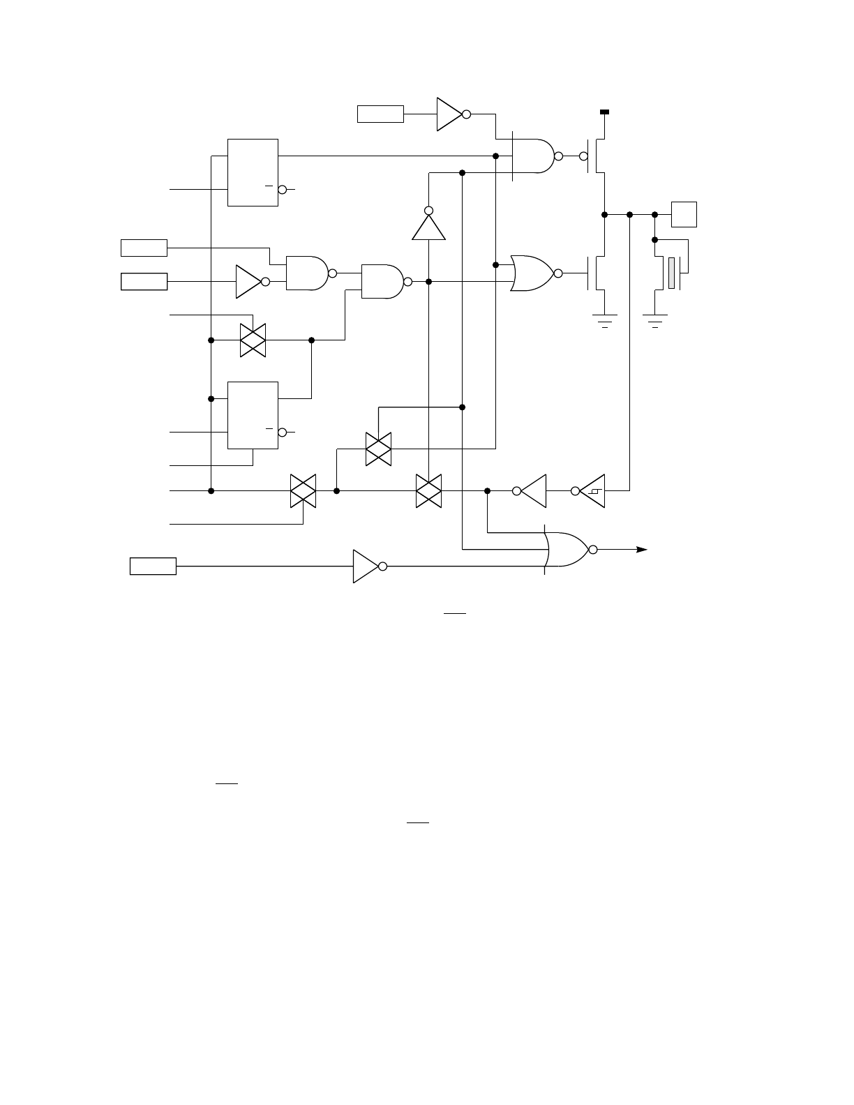
MOTOROLA PARALLEL INPUT/OUTPUT M68HC11
7-36 REFERENCE MANUAL
Figure 7-21 PD5 (SS) Pin Logic
The actual data direction for this port D pin is determined by the logic output of NAND
gate [3]. When the SPI system is disabled, the DDRD bit from HFF [1] controls direc-
tion. When the SPI system is enabled in slave mode, this pin is configured as a high-
impedance input. When the SPI system is enabled in master mode, the DDRD bit from
HFF [1] controls direction. This last condition allows a user to decide how this pin will
be used when the SPI system is configured for master mode. If the DDRD bit is cleared
to zero, this SS pin is used as an input to detect mode faults. If the SPI system is con-
figured so that mode faults would not occur, as in a single-master system, the user can
set the DDRD bit corresponding to the SS pin. In this case, the pin becomes a general-
purpose output pin not associated with the SPI system. The uses and implications of
this logic are discussed in greater detail in SECTION 8 SYNCHRONOUS SERIAL PE-
RIPHERAL INTERFACE.
When the output of NAND gate [3] is one, driver [9] is disabled; thus, the pin is config-
ured as a high-impedance input. To enable pin driver [9], both inputs to NAND gate [3]
must be ones. When the SPI system is disabled, SPE is zero, making the output of
NAND gate [10] a one. This configuration enables NAND gate [3] so that the DDRD
HFF
D
C
Q
R
PD5
VDD
PROTECTION
PIN
N
P
[9]
[1]
DWOM
HFFR
D
C
Q
RDDRD
WPORTD
D5
WDDRD
RPORTD
[2]
[4]
[5] [7]
[6]
[3]
[8]
SPE
RST
[10]
SLAVE ENABLE
TO SPI
SPE [11]
MSTR
Q
Q
[12]

M68HC11 PARALLEL INPUT/OUTPUT MOTOROLA
REFERENCE MANUAL 7-37
bit from HFF [1] can enable or disable driver [9]. When the SPI system is enabled as
a slave, SPE is one, and the master/slave control bit (MSTR) is zero. This configura-
tion causes NAND gate [10] to output zero, which disables output driver [9], regardless
of the state of the DDRD bit at HFF [1]. When the SPI system is enabled as a master,
SPE is one and MSTR is one. This causes NAND gate [10] to output one, which en-
ables NAND gate [3] to control the direction of output buffer [9] based on the state of
the DDRD bit from HFF [1].
Output driver [9] can be placed in a wired-OR configuration by the DWOM control bit.
This control bit simultaneously affects all six port D pins. When DWOM is one, the P-
channel device in the output driver is disabled so the pin cannot be actively driven
high. When the pin attempts to output logic one, the N-channel device is disabled;
thus, the pin appears as a high-impedance input. An external pull-up is used to pas-
sively pull the pin high. The data for output driver [9] comes from the output of HFF [8].
During a write to port D, the WPORTD signal is asserted, which causes data to be
latched into HFF [8] from the internal data bus.
During a read of port D, transmission gate [6] is enabled by the RPORTD signal to cou-
ple data to the internal data bus. The source of data for port D reads depends on the
direction control for the output driver. If the output of NAND gate [3] is zero, output driv-
er [9] is enabled and transmission gate [4] is enabled. In this case, port D reads return
the data from a point inside the output driver. If the output of NAND gate [3] is one,
transmission gate [5] is enabled. In this case, reads of port D return the buffered state
from the pin through inverters [7].
The slave enable signal to the SPI logic is developed by NOR gate [11]. The active-
low SS signal from the pin is buffered by inverters [7] and drives one input of NOR gate
[11]. The other two inputs to this NOR gate act as enables, and the output of the NOR
gate is an active-high slave select signal to the main SPI logic. When the SPI system
is disabled, SPE is zero, disabling NOR gate [11] by forcing its output to zero. When
pin output driver [9] is enabled by a zero at the output of NAND gate [3], NOR gate [11]
is also disabled by the output of inverter [12]. This disabled condition corresponds to
SPI being enabled as a master and the DDRD bit associated with the SS pin being set
to one. In this case, the PD5 pin is being used as a general-purpose output and has
nothing to do with the SPI system. To avoid an erroneous mode fault condition due to
a zero at this pin, the SS signal is disabled to the SPI logic.
7.3.6.7 Idealized Port D Timing
Figure 7-22 shows the idealized timing for important port D control signals. Since this
timing diagram does not consider any propagation delays, it cannot be used as a sub-
stitute for data-sheet timing specifications. This information is useful for understanding
the basis for data-sheet timing specifications so timing information can be extrapolated
for bus frequencies other than that used for the data sheet. Timing information con-
cerning the SPI system is included in SECTION 8 SYNCHRONOUS SERIAL PE-
RIPHERAL INTERFACE.
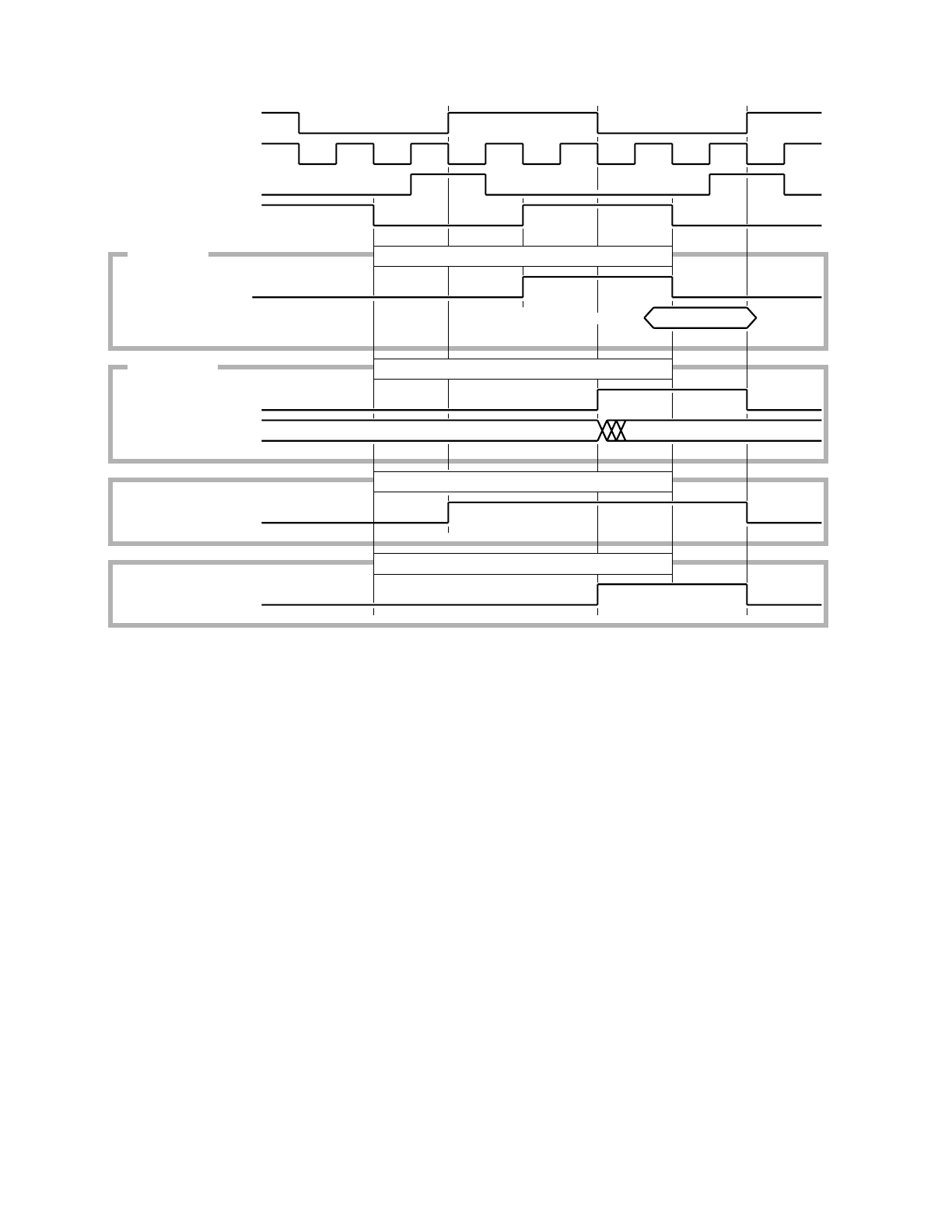
MOTOROLA PARALLEL INPUT/OUTPUT M68HC11
7-38 REFERENCE MANUAL
Figure 7-22 Idealized Port D Timing
On a port D read, the RPORTD signal enables transmission gates that drive port D
data onto the internal data bus. After the RPORTD signal is negated, data is held sta-
ble on the self-latching internal data bus. The CPU actually requires this data to be val-
id for a setup before and hold time after the rising edge of the internal PH2 clock.
Port D writes cause changes to the port D output pins at the falling edge of the internal
PH2 clock. This edge corresponds to the center of the E-clock high time.
During a DDRD read, the RDDRD signal enables a transmission gate to couple the
state of the DDRD bit to the internal data bus. In contrast to the RPORTD signal, RD-
DRD is active while the CPU is actually reading the data from the internal data bus.
Although it should pose no problems to the user, there is a remote chance that the
state of the DDRD bits associated with three of the SPI pins (MISO, MOSI, and SCK)
could change asynchronously with respect to a DDRD read due to a mode fault. In
such a case, the bits in transition could be read incorrectly.
The timing for writes to DDRD is such that the pin configuration will change at the fall-
ing edge of the internal PH2 clock. This edge corresponds to the middle of the E-clock
high time.
NEW PORT D DATA
VALID DATA REQUIRED AT CPU
WRITE TO PORT D
READ FROM PORT D
PH2 (INTERNAL)
EXTAL
AS
PORT D INPUT
RPORTD
PORT D OUTPUT
WPORTD
PORT D OUTPUT PINS
E
RDDRD
READ DDRD
WDDRD
WRITE TO DDRD

M68HC11 PARALLEL INPUT/OUTPUT MOTOROLA
REFERENCE MANUAL 7-39
7.3.7 Port E
The eight port E pins are fixed-direction input pins that also serve as A/D analog chan-
nel inputs. Each of the port E pins has this same logic. The following paragraphs de-
scribe the detailed port E pin logic and the idealized timing of important port E signals.
7.3.7.1 Port E Pin Logic
Figure 7-23 shows the detailed pin logic for one port E pin. When the internal A/D con-
verter system samples a port E pin, N-channel device [1] is enabled to couple the an-
alog level from the port E pin to the sample and hold capacitance in the A/D system.
The enable signal to device [1] is active for the first 12 E-clock cycles of a conversion
cycle for the associated analog channel. A more detailed discussion of the timing of
this enable signal is included in SECTION 12 ANALOG-TO-DIGITAL CONVERTER
SYSTEM. N-channel device [1] and the gate signal driving it are specially designed to
accurately pass analog levels over the full VREFL to VREFH range, even if VREFH is
slightly above VDD.
N- and P-channel devices [2] form an inverter whose input is connected to the pin and
whose output is connected to the similar inverter stage [3]. Unlike a usual CMOS in-
verter, the N-channel device is connected through another series N-channel device to
VSS. This extra device acts as a strobe enable for the inverter. Since the port E pins
are also used as analog inputs, there will be times when the pin is at an intermediate
level. Intermediate levels cause normal CMOS inverters to draw excessive power-sup-
ply currents because both the N- and the P-channel devices can be partially turned on
simultaneously, creating a low-impedance path between VDD and VSS. For port E pins,
this path is interrupted by extra N-channel device [4].
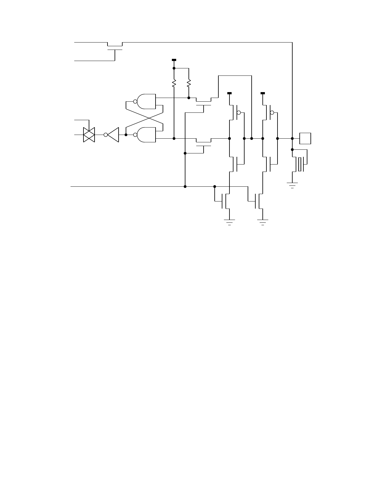
MOTOROLA PARALLEL INPUT/OUTPUT M68HC11
7-40 REFERENCE MANUAL
Figure 7-23 Port E Pin Logic
Four N-channel devices [4] and [5] are used to isolate the potential analog levels at
the port E pins from the digital logic associated with port E. When port E is read digi-
tally, the RPORTE signal is asserted to enable these devices. The devices [4] enable
inverters [2] and [3]. The devices [5] connect the outputs of inverters [2] and [3] to the
set and reset inputs of cross-coupled NAND latch [7]. The RPORTE signal is only as-
serted for one-fourth of an E-clock cycle for the cycle where port E is read. The cross-
coupled NAND latch holds this port E data until later in the read cycle when the CPU
actually reads the data. The A/D read signal (ATDREAD) is asserted during port E
reads to enable transmission gate [8] to couple the data from output latch [7] to the
internal data bus.
Digital reads of port E are not recommended during the sample portion of an A/D con-
version cycle when the gate signal to N-channel device [1] is enabled. The concern is
that enabling inverters [2] and [3] might disturb the analog sample that is occurring.
This disturbance is caused by very tiny gate-to-source and gate-to-drain capacitances
in N- and P-channel devices [2].
7.3.7.2 Idealized Port E Timing
Figure 7-24 shows the idealized timing for important port E control signals. This timing
diagram, which does not consider any propagation delays, cannot be used as a sub-
stitute for data-sheet timing specifications. This information is useful for understanding
PE7–PE0
VDD
PROTECTION
PIN
RPORTE
VDD
VDD
D7–D0
ATDREAD
SAMPLE 8–
SAMPLE 1
TO
CAPACITIVE
DAC
[1]
[2]
[3]
[4]
[5]
[6]
[7]
[8]
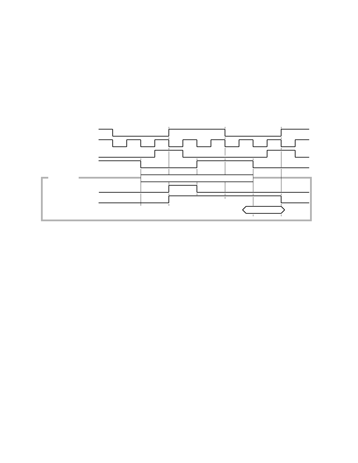
M68HC11 PARALLEL INPUT/OUTPUT MOTOROLA
REFERENCE MANUAL 7-41
the basis for data-sheet timing specifications so timing information can be extrapolated
for bus frequencies other than that used for the data sheet.
On a port E read, the RPORTE signal is asserted for one-fourth E-clock cycle to en-
able the pin input buffers and transfer the digital value from the port E pins into cross-
coupled NAND latches in the pin logic for each port E pin. The ATDREAD signal is also
asserted to enable transmission gates that couple the outputs of the NAND latches to
the internal data bus. Since the CPU does not actually use the data from the NAND
latches until after the RPORTE signal is disabled, the latches are actually acting as
synchronizers for port E data.
Figure 7-24 Idealized Port E Timing
7.4 Handshake I/O Subsystem
The handshake I/O subsystem involves ports B and C, STRA input, STRB output, and
the PIOC register. The following paragraphs explains the strobe and handshake pro-
tocols and the detailed operation of the PIOC register.
There are three primary modes of operation for the handshake I/O subsystem. The
first (default) mode of operation is the simple strobe mode, which uses port B as a sim-
ple strobe output port and port C as a simple latching input port. The second mode of
operation is a full-input handshake; the third mode is a full-output handshake. In the
full-handshake modes of operation, port B is not involved; therefore, it defaults to be-
ing a general-purpose output port.
If the application does not require handshake functions, these functions can generally
be ignored. Ports B and C can be used for simple general-purpose I/O; in fact, the
STRA and STRB pins can even be used for limited non-handshake functions. When
handshake functions are being used, it is usually possible to use any port C pins which
are not needed for handshake as general-purpose I/O pins, without interfering with the
handshake functions of the other port C pins. The one exception to this possibility is
that while full-output handshake is specified, port C pins cannot usually function as
general-purpose input pins. Examples of mixed use of port C pins is presented in 7.4.5
VALID DATA REQUIRED AT CPU
READ FROM PORT E
PH2 (INTERNAL)
EXTAL
AS
PORT E INPUT
RPORTE
ATDREAD
E
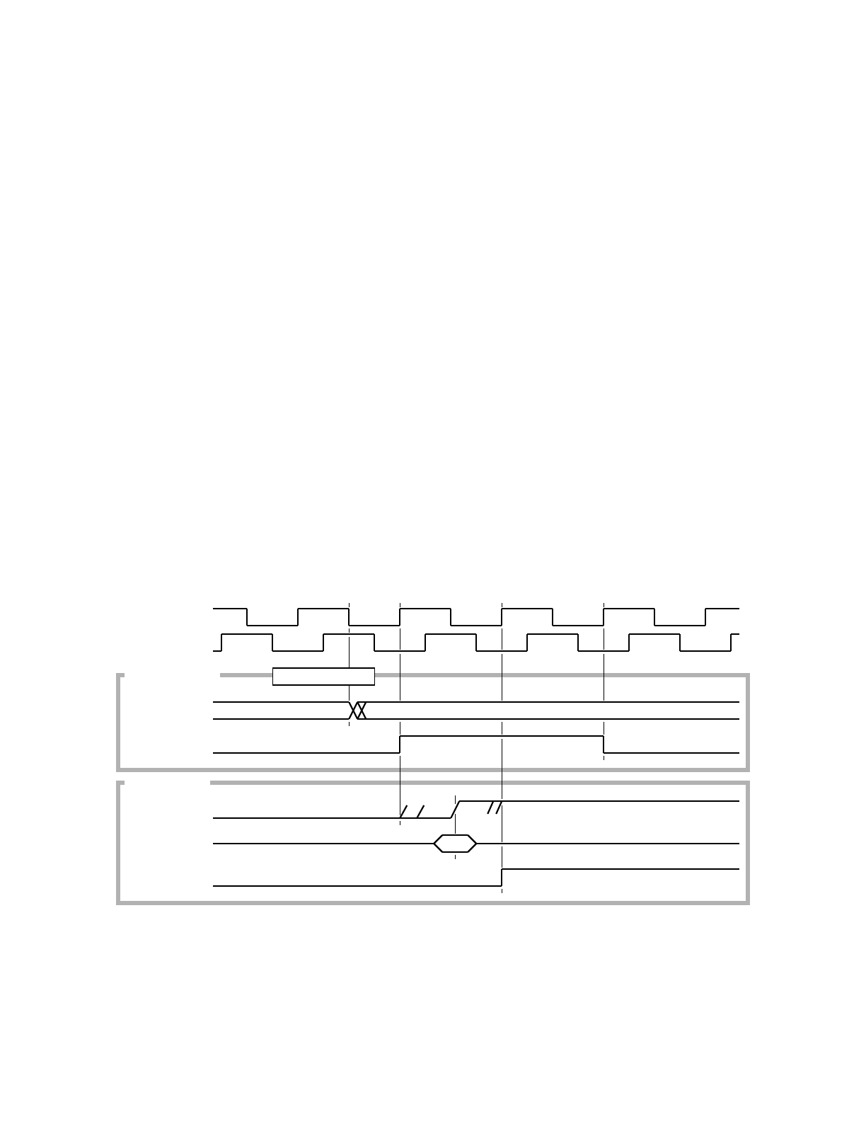
MOTOROLA PARALLEL INPUT/OUTPUT M68HC11
7-42 REFERENCE MANUAL
Non-Handshake Uses of STRA and STRB Pins.
7.4.1 Simple Strobe Mode
The simple strobe mode for the handshake I/O subsystem is selected by HNDS equal
to zero in the PIOC register. At reset, HNDS is forced to zero, which is the default
mode of operation for the handshake I/O subsystem. In this mode, the OIN and PLS
control bits in PIOC have no meaning or effect.
In simple strobe mode, port B is used as a strobe output port in conjunction with the
STRB output pin. Port C is simultaneously used as a latching input port in conjunction
with the STRA input pin. The strobe output function at port B is independent of the
latching input function at port C.
Figure 7-25 shows the idealized timing for simple strobe mode operations in the
MC68HC11A8. The timing for the MC68HC24 is slightly different because the
MC68HC24 does not have access to the internal PH2 clock of the MC68HC11A8. De-
tailed descriptions of the strobe A and strobe B pins are presented in 7.3.3.2 Special
Considerations for STRB on MC68HC24 PRU and 7.3.5.2 Special Considerations
for STRA on MC68HC24 PRU.
7.4.1.1 Port B Strobe Output.
In response to a write to PORTB, data is changed at port B, and then a two E-cycle
pulse is generated at the STRB pin. Although the INVB control bit in PIOC allows a
choice of polarity for strobe B pulses, Figure 7-25 only shows the INVB equals one
case, which selects active-high strobe B pulses.
Figure 7-25 Idealized Timing for Simple Strobe Operations
STROBED OUTPUT
LATCHED INPUT
STAF
PORT C
STROBE A
STROBE B
PORT B
E
PH2 (INTERNAL)
WRITE PORT B
NEW PORT B DATA

M68HC11 PARALLEL INPUT/OUTPUT MOTOROLA
REFERENCE MANUAL 7-43
7.4.1.2 Port C Simple Latching Input
Data at port C is required to be valid for a short setup time before and a short hold time
after the selected edge on the strobe A pin. Since the edge on strobe A is asynchro-
nous, it need not have any special relationship with the E clock. The internal STAF bit,
which indicates that port C data has been latched, must be synchronized with the in-
ternal clocks to avoid setting the flag in the portion of a cycle where it could be read.
This factor implies there may be a delay between when the actual port C data is
latched and when the MCU becomes aware of it. Not counting internal propagation de-
lays, the MC68HC11A8 would have a delay between zero nanoseconds and one E-
clock period. If the relationship between the strobe A edges and the E clock is known,
the user can predict the delay between port C data latching and setting STAF by a
careful study of the strobe A pin description.
7.4.2 Full-input Handshake Mode
Full-input handshake mode is selected when HNDS is one and OIN is zero. In this
mode, the strobe B output acts as a ready signal to an external system. The external
system should not attempt to strobe data into port C until the strobe B signal has been
asserted, indicating a ready condition. The strobe A input is an edge-sensitive latch
command, allowing the external system to asynchronously latch information into port
C.
When a ready condition is recognized, the external device places data on the port D
inputs, then pulses the strobe A input. The active edge on strobe A latches data into
the PORTCL register, sets STAF (optionally causing an interrupt), and negates strobe
B. Negation of strobe B automatically inhibits the external system from strobing any
new data into port C. Reading the latched data from PORTCL (independent of clearing
STAF) causes strobe B to be asserted, indicating new data may now be strobed into
port C.
Control bits allow flexibility to adapt to the requirements of a particular application. The
INVB control bit selects the polarity of the strobe B signals. The EGA determines
whether rising or failing edges will be the active edges for the strobe A input. The PLS
bit determines whether strobe B will operate in pulsed mode or interlocked mode. In
the interlocked mode, strobe B is asserted when the PORTCL register is read and is
negated when an active edge is detected at the strobe A input. In the pulsed mode,
strobe B is asserted when the PORTCL register is read but only remains asserted for
two E-clock cycles.
Figure 7-26 illustrates the full-input handshake protocol. Separate wave forms are in-
cluded to clarify the pulsed versus interlocked modes of strobe B. Although the polarity
of strobe B and the active edge for strobe A can be selected, the figure only shows the
case where INVB and EGA are ones. This configuration specifies strobe A to be sen-
sitive to rising edges and the active level on strobe B to be high. The timing shown in
Figure 7-26 is the idealized timing for the MC68HC11A8. The idealized timing for the
MC68HC24 port replacement unit has small differences, which do not concern most
users.
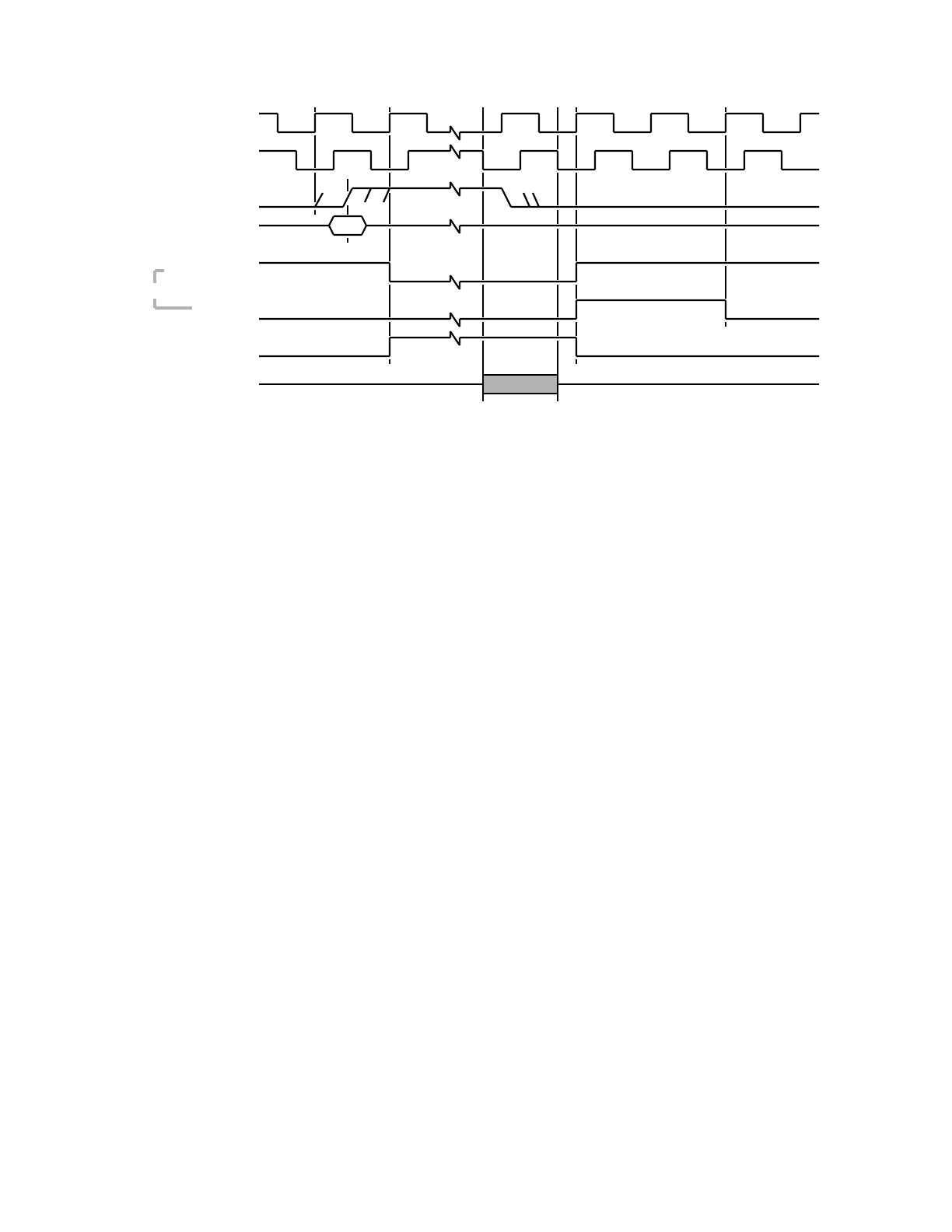
MOTOROLA PARALLEL INPUT/OUTPUT M68HC11
7-44 REFERENCE MANUAL
Figure 7-26 Idealized Timing for Full-Input Handshake
7.4.3 Full-Output Handshake Mode
Full-output handshake mode is selected when HNDS and OIN are ones. In this mode,
port C is used to output data to some external system. The strobe B output signal in-
dicates that port C data is ready for the external system. The strobe A input is pulsed
by the external system to acknowledge that it has accepted the data on port C. In the
three-state variation of output handshake, strobe A also acts like the output enable of
a 74HC244 buffer.
Figure 7-27 illustrates the full-output handshake protocol. This figure shows strobe B
waveforms for both interlocked and pulsed modes. Waveforms are also provided to
show the three-state variation of the output-handshake protocol. Although the polari-
ties for strobes A and B are software programmable, only the case in which EGA and
INVB are ones is shown. This case specifies strobe B is active high, strobe A responds
to rising edges, and the active level on strobe A is low for the three-state variation of
output handshake.
READ PORTCL
(AFTER READING
PIOC WITH STAF=1)
STAF
(PULSED)
(INTERLOCKED)
STROBE B
PORT C
STROBE A
E
PH2 (INTERNAL)
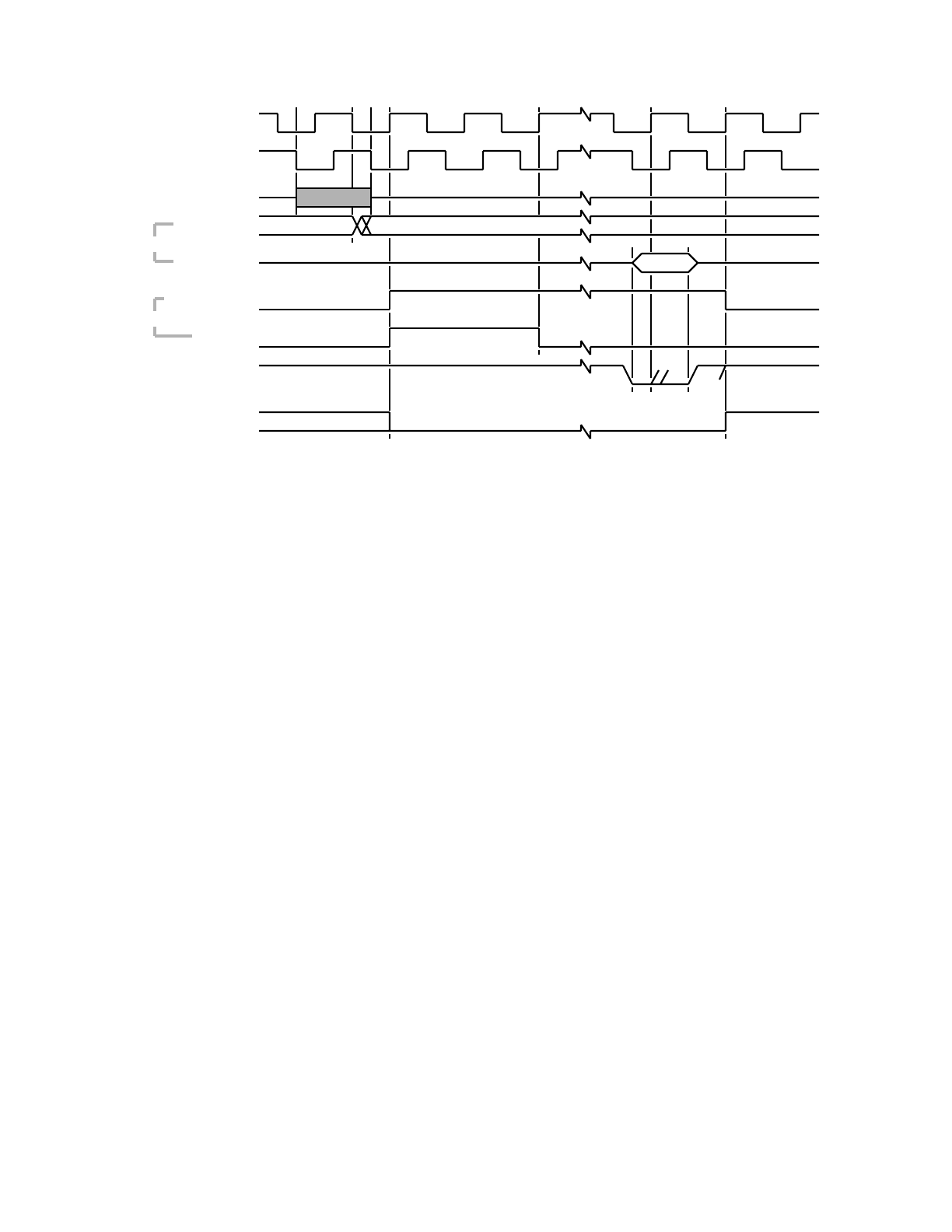
M68HC11 PARALLEL INPUT/OUTPUT MOTOROLA
REFERENCE MANUAL 7-45
Figure 7-27 Idealized Timing for Full-Output Handshake
7.4.3.1 Normal Output Handshake
In an output-handshake transaction, data is output to port C pins by writing to the
PORTCL register, which automatically causes strobe B to be asserted. The external
system recognizes this strobe B signal as a ready indication. After accepting the data
from port C, the external system pulses the strobe A input to acknowledge the receipt
of data. The active edge on strobe A causes strobe B to be negated and STAF to be
set. STAF signals that the MCU can begin the next transaction by writing the next byte
of data to PORTCL.
7.4.3.2 Three-State Variation of Output Handshake
The three-state variation of output handshake can be thought of as if a 74HC244 buffer
had been placed in series with the port C outputs with its output enable connected to
the strobe A signal. The transaction sequence is identical to the normal output hand-
shake protocol previously described.
Port C pins, which are to act as three-state outputs, have their corresponding DDRC
control bits cleared to zero. As long as the strobe A input is at its inactive level, all port
C pins obey their corresponding DDRC specification. When strobe A goes to its active
level, all port C pins act as driven outputs, regardless of their corresponding DDRC
specification. The active level is automatically specified when EGA is selected. If EGA
is zero, failing edges are selected and the active level is high. If EGA is one, rising edg-
es are selected and the active level is low. The relationship between the active edge
and the active level at strobe A was chosen so that the active edge will correspond to
the trailing edge of a port C output enable pulse to strobe A.
E
PH2 (INTERNAL)
(PULSED)
(INTERLOCKED)
STROBE B
(DDR BITS = 0)
(DDR BITS = 1)
PORT C
STROBE A
STAF
WRITE PORTCL
NEW PORT C DATA
DRIVEN

MOTOROLA PARALLEL INPUT/OUTPUT M68HC11
7-46 REFERENCE MANUAL
7.4.4 Parallel I/O Control Register (PIOC)
The PIOC register is used to configure and control the handshake I/O subsystem in
the MC68HC11A8. The following register and paragraphs describe each of the control
or status bits in greater detail.
STAF — Strobe A Flag
This status flag is a key element of the handshake I/O subsystem. Independent of the
strobe or handshake mode, STAF is always set as a result of a selected active edge
at the STRA pin. The edge at STRA, which is asynchronous to the MCU E-clock, caus-
es data to be asynchronously latched into the PORTCL register. The STAF bit is syn-
chronized to the internal PH2 clock. Provided the asynchronous edge occurs at least
a setup time before the rising edge of PH2, STAF will become set at that PH2 rising
edge. If this setup time is not met, then STAF would not be set until the next PH2. The
rising edge of PH2 corresponds to the center of the E-clock low time. The active edge
at STRA is software selectable by the EGA bit in the PIOC register.
The STAF bit is cleared by a two-step, automatic clearing sequence. The first step
arms the clearing mechanism; the second step clears STAF to zero. To arm the clear-
ing mechanism, software reads the PIOC register while the STAF bit is set to one. The
second step depends upon the strobe or handshake mode in effect. In simple strobe
mode (HNDS = 0), the second step of the clearing sequence is to read the PORTCL
register. In full-input handshake mode (HNDS = 1 and OIN = 0), the second step of the
clearing sequence is to read the PORTCL register. In full-output handshake mode
(HNDS = 1 and OIN = 1), the second step of the clearing sequence is to write to the
PORTCL register. The handshake mode can be changed between the arming and
clearing steps of this sequence. If the mode is changed, the action required for the sec-
ond step of the clearing sequence is governed by the state of HNDS and OIN at the
time the second step is performed. Although any amount of delay is permitted between
the two steps of this clearing sequence, it is best to keep the steps as close together
as possible. The arming mechanism is automatically cleared whenever the selected
edge is detected at the STRA pin. If an edge is recognized after the arming step but
before the clearing step, the internal arming signal will be negated, and the clearing
step will not clear STAF.
STAI — Strobe A Interrupt Enable
This control bit determines whether STAF will cause interrupts. When STAI is one, a
hardware interrupt request is generated whenever the STAF bit is set. When STAI is
zero, STAF interrupts are inhibited.
CWOM — Port C Wired-OR Mode
This bit is used to configure all port C outputs for wired-OR operation. When CWOM
is zero, port C outputs operate as active push-pull drivers. When CWOM is one, the
P-type pull-up devices are disabled, causing port C outputs to act as open-drain driv-
PIOC — Parallel I/O Control Register $1002
BIT 7 654321BIT 0
STAF STAI CWOM HNDS OIN PLS EGA INVB
RESET: 00000U11

M68HC11 PARALLEL INPUT/OUTPUT MOTOROLA
REFERENCE MANUAL 7-47
ers. The CWOM bit simultaneously affects all eight port C bits. The P-channel device
forms a P-N junction between the VDD supply and the output pin so that the pin cannot
be pulled more than a diode drop above the VDD supply. For this reason, the wired-
OR mode cannot be used for level conversion the way open-collector TTL devices are
sometimes used. In a TTL system, a brief contention between two push-pull drivers,
though not good practice, generally has no serious consequences. In a CMOS sys-
tem, a brief contention between push-pull drivers can induce destructive latchup. In
cases where two CMOS output drivers could be in contention, they should be config-
ured for wired-OR operation. If there is a brief contention between the time one driver
is turned on and the other is turned off, there will be no danger of latchup damage.
HNDS — Handshake/Simple Strobe Mode Select
When HNDS is zero, the simple strobe mode is selected. In the simple strobe mode,
the STRB pin is pulsed for two E-clock cycles after each write to port B. Also, port C
data is asynchronously latched into the PORTCL register each time the selected edge
is detected at the STRA pin. When HNDS is set to one, either full-input or full-output
handshake mode is selected. All full-handshake modes use port C, the STRA strobe
input pin, and the STRB handshake output pin. Since the handshake I/O subsystem
does not use port B when a full-handshake mode is selected, port B defaults to being
a general-purpose output port.
OIN — Output/Input Handshake Select
This bit has no effect unless HNDS is one. When HNDS is one, OIN further qualifies
the handshake mode. When OIN is one, full-output handshake is selected. When OIN
is zero, full-input handshake is selected.
PLS — Strobe B Pulse Mode Select
This control bit determines whether the STRB pin is configured for pulsed or inter-
locked operation. In interlocked mode, once STRB is asserted, it will remain active un-
til an acknowledge edge is detected at the STRA pin. The interlocked mode is selected
when PLS is zero. Interlocked mode cannot be specified unless HNDS is logic one. In
pulsed mode, STRB is negated exactly two E-clock cycles after it is asserted. When
the simple strobe mode is selected (HNDS = 0), the pulsed mode is assumed, even if
PLS is set to one. Additional information about strobe B can be found in 7.3.3 R/W
(STRB) Pin.
EGA — Edge Select for Strobe A
This control bit selects which polarity edge will be recognized at the STRA input pin.
When EGA is zero, falling edges are detected and rising edges are ignored. When
EGA is one, only rising edges are recognized at the STRA pin. When the three-state
variation of the full-output handshake mode is being used, EGA also specifies the level
on STRA that will cause port C output buffers to be enabled. The output enable for port
C pins is an active-high internal signal, which is the exclusive OR of EGA with the level
at the STRA pin. Thus, the trailing edge of the enable signal on the STRA pin will be
the selected active edge used by the handshake sequence.
INVB — Invert Strobe B
The STRB signal is developed in an S/R flip-flop in the STRB pin logic. The INVB con-
trol bit selects either the Q or Q output of this flip-flop to be coupled out of the STRB

MOTOROLA PARALLEL INPUT/OUTPUT M68HC11
7-48 REFERENCE MANUAL
pin. If INVB is zero, the Q of this latch is coupled out of the STRB pin, and STRB sig-
nals are active low. If INVB is one, the Q of this latch is used, and STRB signals are
active high. Changes to INVB do not affect the state of the internal S/R flip-flop.
7.4.5 Non-Handshake Uses of STRA and STRB Pins
When not being used for handshake functions, the STRA pin can be used as a gener-
al-purpose edge-detection interrupt source, which is fairly common use for the STRA
pin. The STAF is set each time a selected edge is recognized. The STAI control bit
allows strobe A edges to force a maskable interrupt to the IRQ vector. The EGA control
bit allows the user to select either rising edges or falling edges as the triggering edge
for the strobe A input.
Though not a very common practice, the STRB pin can be used as an extra static out-
put. When full-input handshake mode is selected, STRB remains at its inactive level
until the PORTCL register is read. If PORTCL is never read, STRB stays at its inactive
level indefinitely. The INVB control bit allows the user to switch the inactive level from
one to zero by writing to the PIOC register. In this scheme, it is important never to read
the PORTCL register because this would cause STRB to automatically go to its active
level. Other similar schemes may be developed to meet specific application needs.
Usually when the STRA and STRB pins are being used for non-handshake functions,
the handshake I/O subsystem would be configured for full-input handshake mode be-
cause the other two modes result in interactions between the strobe pins and the port
B and C pins. If simple strobe mode is selected, any write to port B will generate a
pulse on the STRB pin. If full-output handshake is selected, each time the STRA pin
goes to its selected active level, all port C pins are forced to be outputs (even if the
DDRC bits indicate they should be inputs). These interactions are a normal conse-
quence of the handshake I/O functions but could interfere with non-handshake use of
the STRA and STRB pins. For this reason, users are encouraged to study the opera-
tion of the handshake I/O subsystem carefully if they plan to use STRA and STRB for
non-handshake functions.

M68HC11 SYNCHRONOUS SERIAL PERIPHERAL INTERFACE MOTOROLA
REFERENCE MANUAL 8-1
SECTION 8
SYNCHRONOUS SERIAL PERIPHERAL INTERFACE
The serial peripheral interface (SPI) is one of two independent serial communications
subsystems included on the MC68HC11A8. As the name implies, the SPI is primarily
used to allow the microcontroller unit (MCU) to communicate with peripheral devices.
The SPI is also capable of interprocessor communications in a multiple-master sys-
tem. Peripheral devices are as simple as an ordinary transistor-transistor logic (TTL)
shift register or as complex as a complete subsystem, such as a liquid crystal diode
(LCD) display driver or an analog-to-digital (A/D) converter subsystem. The SPI sys-
tem is flexible enough to interface directly with numerous standard product peripherals
from several manufacturers. The system can be configured as a master or a slave de-
vice. Data rates as high as 1 Mbit per second are accommodated when the system is
configured as a master; rates as high as 2 Mbits per second are accommodated when
the system is operated as a slave.
Clock control logic allows a selection of clock polarity and a choice of two fundamen-
tally different clocking protocols to accommodate most available synchronous serial
peripheral devices. When the SPI is configured as a master, software selects one of
four different bit rates for the serial clock.
Error-detection logic is included to support interprocessor communications. A write-
collision detector indicates when an attempt is made to write data to the serial shift reg-
ister while a transfer is in progress. A multiple-master mode-fault detector automatical-
ly disables SPI output drivers if more than one MCU simultaneously attempts to
become bus master.
The I/O pin control logic on the MC68HC11A8 is more flexible than that of other Mo-
torola MCUs. This added I/O pin control allows the MC68HC11A8 to implement sys-
tems with a single, bidirectional data line or other unusual synchronous serial
configurations.
8.1 SPI Transfer Formats
During an SPI transfer, data is simultaneously transmitted (shifted out serially) and re-
ceived (shifted in serially). A serial clock line synchronizes shifting and sampling of the
information on the two serial data lines. A slave select line allows individual selection
of a slave SPI device; slave devices that are not selected do not interfere with SPI bus
activities. On a master SPI device, the slave select line can optionally be used to indi-
cate a multiple-master bus contention.
8.1.1 SPI Clock Phase and Polarity Controls
Software can select any of four combinations of serial clock (SCK) phase and polarity
using two bits in the SPI control register (SPCR). The clock polarity is specified by the
CPOL control bit, which selects an active high or active low clock and has no signifi-
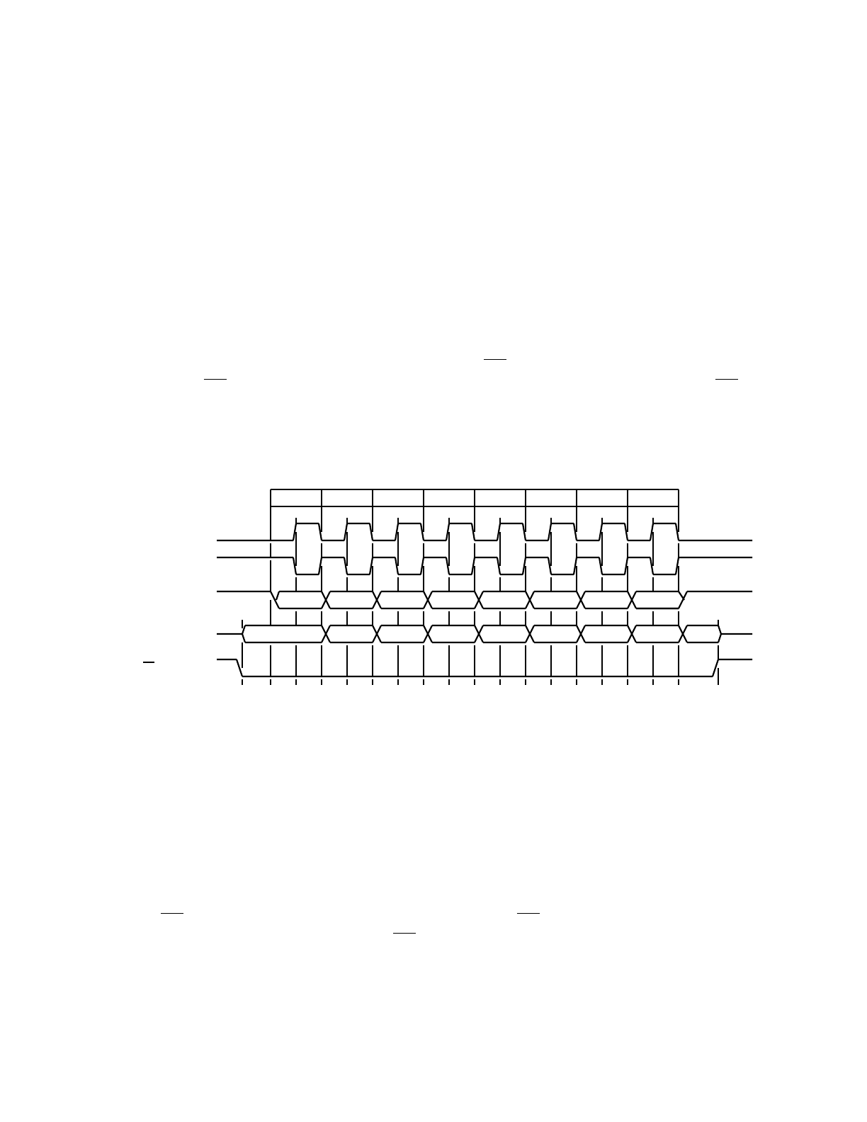
MOTOROLA SYNCHRONOUS SERIAL PERIPHERAL INTERFACE M68HC11
8-2 REFERENCE MANUAL
cant effect on the transfer format. The clock phase (CPHA) control bit selects one of
two fundamentally different transfer formats. The clock phase and polarity should be
identical for the master SPI device and the communicating slave device. In some cas-
es, the phase and polarity are changed between transfers to allow a master device to
communicate with peripheral slaves having different requirements. The flexibility of the
SPI system on the MC68HC11A8 allows direct interface to almost any existing syn-
chronous serial peripheral.
8.1.2 CPHA Equals Zero Transfer Format
Figure 8-1 is a timing diagram of an SPI transfer where CPHA is zero. Two waveforms
are shown for SCK: one for CPOL equals zero and another for CPOL equals one. The
diagram may be interpreted as a master or slave timing diagram since the SCK, mas-
ter in/slave out (MISO), and master out/slave in (MOSI) pins are directly connected be-
tween the master and the slave. The MISO signal is the output from the slave, and the
MOSI signal is the output from the master. The SS line is the slave select input to the
slave; the SS pin of the master is not shown but is assumed to be inactive. The SS pin
of the master must be high or must be reconfigured as a general-purpose output not
affecting the SPI. This timing diagram functionally depicts how a transfer takes place;
it should not be used as a replacement for data-sheet parametric information.
Figure 8-1 CPHA Equals Zero SPI Transfer Format
8.1.3 CPHA Equals One Transfer Format
Figure 8-2 is a timing diagram of an SPI transfer where CPHA is one. Two waveforms
are shown for SCK: one for CPOL equals zero and another for CPOL equals one. The
diagram may be interpreted as a master or slave timing diagram since the SCK, MISO,
and MOSI pins are directly connected between the master and the slave. The MISO
signal is the output from the slave, and the MOSI signal is the output from the master.
The SS line is the slave select input to the slave; the SS pin of the master is not shown
but is assumed to be inactive. The SS pin of the master must be high or must be re-
configured as a general-purpose output not affecting the SPI. This timing diagram
functionally illustrates how a transfer takes place; it should not be used as a replace-
ment for data-sheet parametric information.
MSB 654321LSB
*
654321LSB
Not defined but normally MSB of character just received.
23456781
MSB
MISO
(FROM SLAVE)
MOSI
(FROM MASTER)
SCK (CPOL=1)
SCK (CPOL=0)
SCK CYCLE #
(FOR REFERENCE)
SS (TO SLAVE)
LSB
*
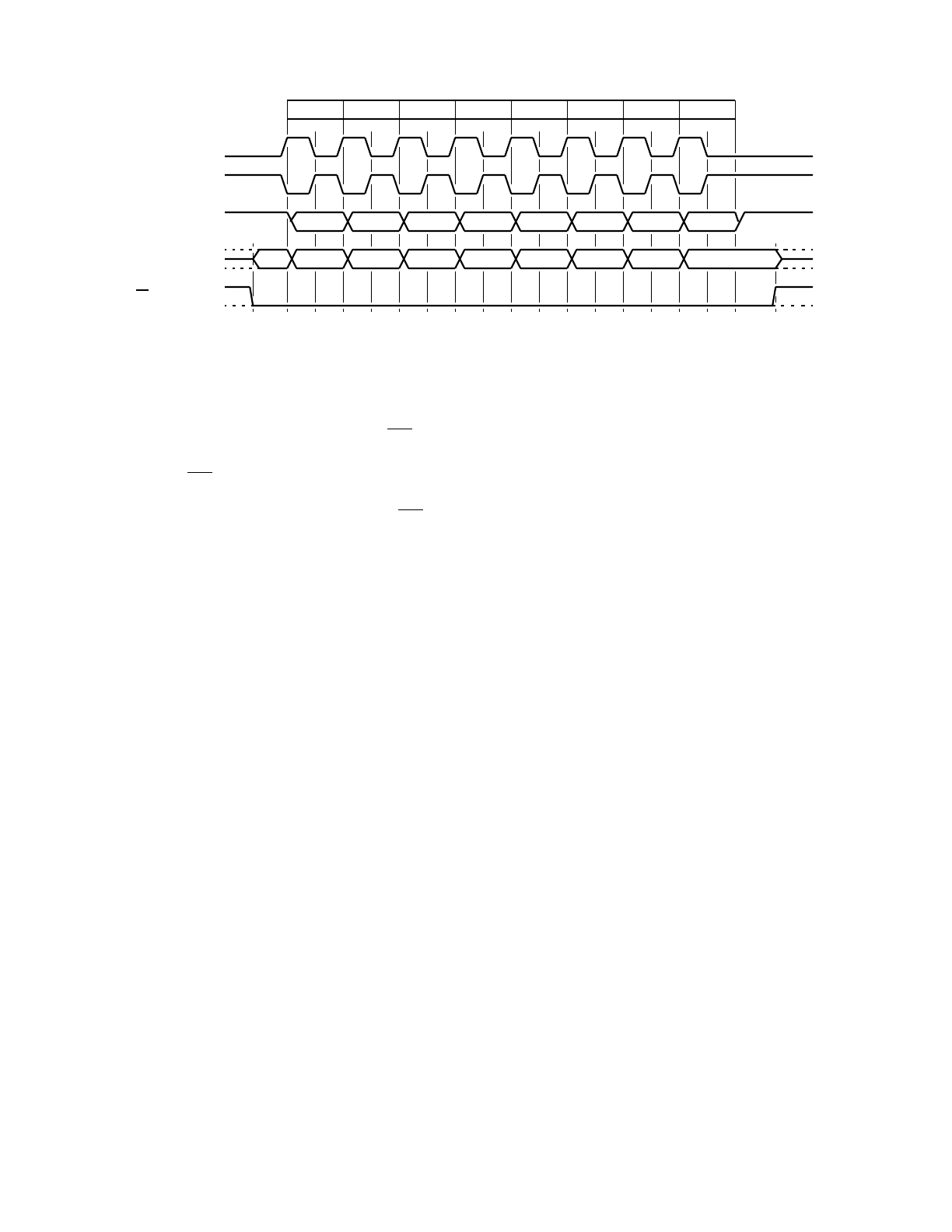
M68HC11 SYNCHRONOUS SERIAL PERIPHERAL INTERFACE MOTOROLA
REFERENCE MANUAL 8-3
Figure 8-2 CPHA Equals One SPI Transfer Format
When CPHA equals zero, the SS line must be negated and reasserted between each
successive serial byte. Also, if the slave writes data to the SPI data register (SPDR)
while SS is active low, a write-collision error results.
When CPHA equals one, the SS line may remain active low between successive
transfers (can be tied low at all times). This format is sometimes preferred in systems
having a single fixed master and a single slave driving the MISO data line.
8.2 SPI Block Diagram
Figure 8-3 is a block diagram of the SPI subsystem. When an SPI transfer occurs, an
8-bit character is shifted out one data pin while a different 8-bit character is simulta-
neously shifted in a second data pin. Another way to view this transfer is that an 8-bit
shift register in the master and another 8-bit shift register in the slave are connected
as a circular 16-bit shift register. When a transfer occurs, this distributed shift register
is shifted eight bit positions; thus, the characters in the master and slave are effectively
exchanged.
The central element in the SPI system is the block containing the shift register and the
read data buffer. The system is single buffered in the transmit direction and double
buffered in the receive direction. This fact means new data for transmission cannot be
written to the shifter until the previous transaction is complete; however, received data
is transferred into a parallel read data buffer so the shifter is free to accept a second
serial character. As long as the first character is read out of the read data buffer before
the next serial character is ready to be transferred, no overrun condition will occur. A
single MCU register address is used for reading data from the read data buffer and for
writing data to the shifter.
Not defined but normally LSB of previously transmitted character.
654321 LSB
654321LSB
23456781
MSB
MISO
(FROM SLAVE)
MOSI
(FROM MASTER)
SCK (CPOL=1)
SCK (CPOL=0)
SCK CYCLE #
(FOR REFERENCE)
SS (TO SLAVE)
MSB
∗
∗
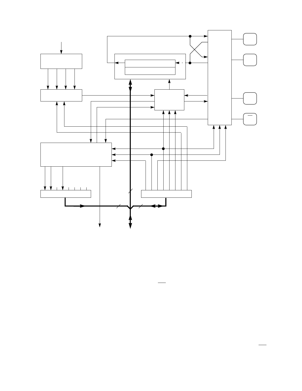
MOTOROLA SYNCHRONOUS SERIAL PERIPHERAL INTERFACE M68HC11
8-4 REFERENCE MANUAL
Figure 8-3 SPI System Block Diagram
8.3 SPI Pin Signals
There are four I/O pin signals associated with SPI transfers: the SCK, the MISO data
line, the MOSI data line, and the active low SS pin. When the SPI system is disabled,
the four pins are configured for general-purpose I/O, and the primary direction of data
is controlled by a data direction control bit corresponding to each I/O pin. When the
SPI system is enabled, the data direction control bits still influence the direction of data
at the pins. Detailed logic for these pins is included in SECTION 7 PARALLEL INPUT/
OUTPUT. The following rules will answer the most common questions. When the SPI
system is on and expects a pin to be an input, the pin will be configured as an input
regardless of the state of its data direction control bit. When the SPI system is on and
expects a pin to be an output, the pin will be configured as an output only if its data
direction control bit is set to one. When the SPI is configured as a master, the PD5/SS
SPR0
SPR1
CPHA
CPOL
MSTR
DWOM
SPE
SPIE
SPI CONTROL REGISTER
MODF
WCOL
SPIF
SPI STATUS REGISTER
8/16-BIT SHIFT REGISTER
READ DATA BUFFER
MSB LSB
INTERNAL
DATA BUS
SPI INTERRUPT
REQUEST
MSTR
SPE
MSTR
DWOM
SPE
SPR0
SPI CLOCK (MASTER)
SPI CONTROL
SELECT
DIVIDER
INTERNAL
MCU CLOCK
CLOCK
LOGIC
CLOCK
PIN CONTROL LOGIC
S
M
S
M
M
S
MISO
PD2
MOSI
PD3
SCK
PD4
SS
PD5
SPR1
÷2÷4÷16 ÷32
8 8
8

M68HC11 SYNCHRONOUS SERIAL PERIPHERAL INTERFACE MOTOROLA
REFERENCE MANUAL 8-5
pin is a special case.
NOTE
SPI transfers will not occur unless the outputs are enabled by setting
the corresponding DDRD bits. SPI outputs are disabled (high imped-
ance) unless their corresponding DDRD bits are set to one. SPI
inputs are configured as high-impedance inputs even if their corre-
sponding DDRD bits are set to one.
The SCK pin is an output when the SPI is configured as a master and an input when
the SPI is configured as a slave. When the SPI is configured as a master, the SCK
signal is derived from the internal MCU bus clock. When the master initiates a transfer,
eight clock cycles are automatically generated on the SCK pin. When the SPI is con-
figured as a slave, the SCK pin is an input, and the clock signal from the master syn-
chronizes the data transfer between the master and slave devices. Slave devices
ignore the SCK signal unless the slave select pin is active low. In both the master and
slave SPI devices, data is shifted on one edge of the SCK signal and is sampled on
the opposite edge where data is stable. Edge polarity is determined by the SPI transfer
protocol.
The MISO and MOSI data pins are used for transmitting and receiving serial data.
When the SPI is configured as a master, MISO is the master data input line, and MOSI
is the master data output line. When the SPI is configured as a slave, these pins re-
verse roles. In a multiple-master system, all SCK pins are tied together, all MOSI pins
are tied together, and all MISO pins are tied together. A single SPI device is configured
as a master; all other SPI devices on the SPI bus are configured as slaves. The single
master drives data out its SCK and MOSI pins to the SCK and MOSI pins of the slaves.
One selected slave device optionally drives data out its MISO pin to the MISO master
pin. The automatic control of the direction of these pins makes reconfiguration through
external logic unnecessary when a new device becomes the master.
The SS pin behaves differently on master and slave devices. On a slave device, this
pin is used to enable the SPI slave for a transfer. If the SS pin of a slave is inactive
(high), the device ignores SCK clocks and keeps the MISO output pin in the high-im-
pedance state. On a master device, the SS pin can optionally serve as an error-detec-
tion input for the SPI or as a general-purpose output not affecting the SPI. The choice
is based on the corresponding data direction control bit (DDRD5). When DDRD5 is
logic one and the SPI is configured as a master, the PD5/SS pin acts as a general-
purpose output that is independent of SPI activities. When the DDRD5 bit is logic zero
and the SPI system is configured as a master, the SS pin acts as an error-detection
input, which should remain high. If the SS pin goes low while the SPI is a master and
is using the SS pin as an error-detection input, it indicates that some other device on
the SPI bus is attempting to be a master. This attempt causes the master device sens-
ing the error to immediately exit the SPI bus to avoid potentially damaging driver con-
tentions. This detection is called a mode fault and is discussed in 8.5.1 SPI Mode-
Fault Error.
The port D I/O pins, including the four SPI pins, can be configured to behave as open-

MOTOROLA SYNCHRONOUS SERIAL PERIPHERAL INTERFACE M68HC11
8-6 REFERENCE MANUAL
drain drivers. The port D wired-OR mode (DWOM) control bit is used to enable this
option. An external pull-up resistor is required on each port D output pin while this op-
tion is selected. In multiple-master systems, this option provides extra protection
against CMOS latchup because, even if more than one SPI device tries to simulta-
neously drive the same bus line, there will be no destructive contention. Other unusual
SPI system configurations also benefit from this option (e.g., when MISO and MOSI
are tied together to form a single, bidirectional data line).
8.4 SPI Registers
The SPI control register (SPCR), SPI status register (SPSR), and SPDR are software-
accessible registers used to configure and operate the SPI system. Because the port
D data direction control register (DDRD) influences SPI activities, it will be discussed
briefly. Detailed logic diagrams of the port D pins can be found in SECTION 7 PAR-
ALLEL INPUT/OUTPUT.
8.4.1 Port D Data Direction Control Register (DDRD)
This register, which may be read or written at any time, is used to control the primary
direction of port D pins. Bits 5, 4, 3, and 2 of port D are used by the SPI system when
the SPI enable (SPE) control bit is one. The serial communications interface (SCI) sys-
tem uses the other two bits of port D when the SCI receiver and transmitter are en-
abled. This description of DDRD is only intended to cover material related to the SPI
system.
DDRD5 — Data Direction Control for Port D Bit 5 (SS)
When the SPI system is enabled as a slave (SPE = 1; MSTR = 0), the PD5/SS pin is
the slave select input, regardless of the value of DDRD5. When the SPI system is en-
abled as a master (SPE = 1; MSTR = 1), the function of the PD5/SS pin depends on
the value in DDRD5.
0 = The SS pin is used as an input to detect mode-fault errors. A low on this pin
indicates that some other device in a multiple-master system has become a
master and is trying to select this MCU as a slave. To prevent harmful conten-
tions between output drivers, a mode fault is generated, which causes the de-
vice sensing the fault to immediately change all of its SPI pins to high
impedance. Additional information on mode faults is given in 8.5.1 SPI Mode-
Fault Error.
1 = The PD5/SS pin acts as a general-purpose output not affected by the SPI sys-
tem. Because the mode-fault detection logic in the SPI is disabled, changing
this PD5 output pin to zero does not affect the SPI system.
DDRD4 — Data Direction Control for Port D Bit 4 (SCK)
DDRD — Port D Data Direction Register $1009
BIT 7 654321BIT 0
— — DDRD5 DDRD4 DDRD3 DDRD2 DDRD1 DDRD0
RESET: 00000000
REFER-
ENCE: — — TS SCK MOSI MISO TxD RxD

M68HC11 SYNCHRONOUS SERIAL PERIPHERAL INTERFACE MOTOROLA
REFERENCE MANUAL 8-7
When the SPI system is enabled as a slave, the PD4/SCK pin acts as the SPI serial
clock input, regardless of the state of DDRD4. When the SPI system is enabled as a
master, the DDRD4 bit must be set to one to enable the SCK output.
DDRD3 — Data Direction Control for Port D Bit 3 (MOSI)
When the SPI system is enabled as a slave, the PD3/MOSI pin acts as the slave serial
data input, regardless of the state of DDRD3.
When the SPI system is enabled as a master, the DDRD3 bit must be set to one to
enable the master serial data output. If a master device wants to initiate an SPI transfer
to receive a byte of data from a slave without transmitting a byte, it might purposely
leave the MOSI output disabled. SPI systems that tie MOSI and MISO together to form
a single bidirectional data line also need to selectively disable the MOSI output.
DDRD2 — Data Direction Control for Port D Bit 2 (MISO)
When the SPI system is enabled as a slave, the DDRD2 bit must be set to one to en-
able the slave serial data output. A master SPI device can simultaneously broadcast
a message to several slaves as long as no more than one of the slaves tries to drive
the MISO line. SPI systems that tie MOSI and MISO together to form a single bidirec-
tional data line also need to selectively disable the MISO output.
When the SPI system is enabled as a master, the PD2/MISO pin acts as the master
serial data input, regardless of the state of DDRD2.
8.4.2 SPI Control Register (SPCR)
This register, which may be read or written at any time, is used to configure the SPI
system. The DDRD register must also be properly configured before SPI transfers can
occur.
SPIE — SPI Interrupt Enable
0 = SPI interrupts are disabled. Polling is used to sense the SPIF and MODF flags.
1 = SPI interrupt is requested if SPIF or MODF set (provided I bit in condition code
register (CCR) is zero).
SPE — SPI System Enable
0 = SPI system is off.
1 = SPI system is on.
DWOM — Port D Wired-OR Mode Select
0 = Port D outputs are push-pull.
1 = P-channel pull-ups on all six port D output drivers are disabled so port D outputs
act as open-drain drivers.
MSTR — Master/Slave Mode Select
0 = SPI is configured as a slave.
SPCR — SPI Control Register $1028
BIT 7 654321BIT 0
SPIE SPE DWOM MSTR CPOL CPHA SPR1 SPR0
RESET: 000001UU
MOTOROLA SYNCHRONOUS SERIAL PERIPHERAL INTERFACE M68HC11
8-8 REFERENCE MANUAL
1 = SPI is configured as a master.
CPOL — Clock Polarity Select
0 = Active high clocks selected; SCK idles low.
1 = Active low clocks selected; SCK idles high.
CPHA — Clock Phase Select
This control bit selects one of two fundamentally different transfer formats (see 8.1 SPI
Transfer Formats).
SPR1, SPR0 — SPI Bit Rate Select
The following table shows the relationship between the SPR1 and SPR0 control bits
and the bit rate for transfers when the SPI is operating as a master. When the SPI is
operating as a slave, the serial clock is input from the master; therefore, the SPR1 and
SPR0 control bits have no meaning.
8.4.3 SPI Status Register (SPSR)
This read-only register contains status flags indicating the completion of an SPI trans-
fer and the occurrence of certain SPI system errors. The flags are automatically set by
the occurrence of the corresponding SPI events; the flags are cleared by automatic
software sequences.
SPIF — SPI Transfer Complete Flag
This flag is automatically set to one at the end of an SPI transfer. SPIF is automatically
cleared by reading the SPSR with SPIF set, followed by an access of the SPDR. The
definition of end of a transfer varies with master versus slave and the transfer format
specified by CPHA. This subject is discussed in 8.6 Beginning and Ending SPI
Transfers.
WCOL — Write Collision Error Flag
This flag is automatically set if the SPDR is written while a transfer is in progress.
WCOL is automatically cleared by reading the SPSR with WCOL set, followed by an
access of the SPDR. The details of when a transfer technically begins and ends de-
pend on the configuration of the SPI system, which is discussed in 8.6 Beginning and
Ending SPI Transfers.
SPR1 SPR0 E Clock
Divided By
002
014
1016
1132
SPSR — SPI Status Register $1029
BIT 7 654321BIT 0
SPIF WCOL — MODF ————
RESET: 00000000

M68HC11 SYNCHRONOUS SERIAL PERIPHERAL INTERFACE MOTOROLA
REFERENCE MANUAL 8-9
Bit 5 — Not implemented; always reads zero.
MODF — Mode-Fault Error Flag
This flag is set if the SS signal goes to active low while the SPI is configured as a mas-
ter (MSTR = 1). MODF is automatically cleared by reading the SPSR with MODF set,
followed by a write to the SPCR. Because the mode-fault mechanism is intended to
prevent damage due to conflicts between output drivers, it takes effect immediately,
regardless of the SPI system configuration at the time of the fault. The MSTR control
bit in the SPCR and all four DDRD control bits associated with the SPI are cleared,
and an interrupt is generated subject to masking by the SPIE control bit and the I bit
in the CCR. Mode-fault errors are discussed in greater detail in the following para-
graphs.
Bits [3:0] — Not implemented; always read zero.
8.5 SPI System Errors
Two system errors can be detected by the SPI system in the MC68HC11A8. The first
type error arises in a multiple-master system when more than one SPI device simulta-
neously tries to be a master. This error is called a mode fault. The second type error,
a write collision, indicates that an attempt has been made to write data to the SPDR
while a transfer was in progress.
8.5.1 SPI Mode-Fault Error
When the SPI system is configured as a master and the SS input line goes to active
low, a mode-fault error has occurred. Only an SPI master can experience a mode-fault
error, caused when a second SPI device becomes a master and selects this device as
if it were a slave. In cases where more than one device is concurrently configured as
a master, there is a chance of contention between two pin drivers. For push-pull CMOS
drivers, this contention can cause catastrophic latchup. When this type error is detect-
ed, the following actions are taken immediately:
1. The DDRD bits corresponding to the four SPI-related I/O pins are forced to zero
to disable all SPI output drivers.
2. The MSTR control bit is forced to zero to reconfigure the SPI as a slave.
3. The SPE control bit is forced to zero to disable the SPI system.
4. The MODF status flag is set, and an SPI interrupt is generated subject to mask-
ing by the SPIE bit and the I bit in the CCR.
After software has corrected the problems that led to the mode fault, MODF is cleared
and the system is returned to normal operation. The MODF flag is automatically
cleared by reading SPSR while MODF is set, followed by a write to the SPDR. The
DDRD must also be restored before SPI transfers can resume.
In some cases, the mode-fault mechanism does not fully protect multiple-master sys-
tems from driver contention. For example, suppose a second device becomes a mas-
ter but does not immediately drive the SS pin of this master low. Perhaps a system
fault selects two slave devices, and these slave devices try to simultaneously drive the

MOTOROLA SYNCHRONOUS SERIAL PERIPHERAL INTERFACE M68HC11
8-10 REFERENCE MANUAL
MISO line. Both these cases result in output driver contentions, but neither causes a
mode-fault error. Too many system configurations are possible to discuss all the pos-
sibilities, but some suggestions will help the system designer find practical ways to
prevent problems.
Under normal conditions, a moderate resistance, (i.e., 1 to 10K ohms) in series with
an SPI pin does not adversely affect SPI transfer operations. If a driver contention oc-
curs, this series resistance will protect the drivers against latchup. Another way to pro-
tect against latchup would be to employ the DWOM option, which transforms the SPI
output drivers into open-drain-type drivers. When the DWOM option is selected, it af-
fects all six port D pins; therefore, pull-up resistors are needed on the PD0 and PD1
pins if they are being used as outputs. Both of these suggestions affect the maximum
usable data rate, depending on the loading capacitance on the SPI lines.
8.5.2 SPI Write-Collision Errors
A write collision occurs if the SPDR is written while a transfer is in progress. Since the
SPDR is not double buffered in the transmit direction, writes to SPDR cause data to
be written directly into the SPI shift register. Because this write corrupts any transfer
in progress, a write-collision error is generated. The transfer continues undisturbed,
and the write data that caused the error is not written to the shifter.
A write collision is normally a slave error because a slave has no control over when a
master will initiate a transfer. A master knows when a transfer is in progress; thus,
there is no excuse for a master to generate a write-collision error, although the SPI log-
ic can detect write collisions in a master as well as in a slave.
The details of what constitutes a transfer in progress depend on the SPI configuration.
For a master, a transfer starts when data is written to SPDR and ends when SPIF is
set. For a slave with CPHA equals zero, a transfer starts when SS goes low and ends
when SS returns high. In this instance, SPIF is set at the middle of the eighth SCK cy-
cle when data is transferred from the shifter to the parallel data register, but the trans-
fer is still in progress until SS goes high. For a slave with CPHA equals one, a transfer
starts when the SCK line goes to its active level, which is the edge at the beginning of
the first SCK cycle. The transfer ends in a slave in which CPHA equals one when SPIF
is set.
8.6 Beginning and Ending SPI Transfers
The two basic SPI transfer formats are described in 8.1 SPI Transfer Formats.A
transfer includes the eight SCK cycles plus an initiation period at the beginning and
ending period of the transfer. The details of the beginning and ending periods depend
on the CPHA format selected and whether the SPI is configured as a master or a
slave. The initiation delay period is also affected by the SPI clock rate selection when
the SPI is configured as a master.
It may be useful to refer to the transfer format illustrated in Figure 8-1 and Figure 8-2
to understand how the beginning and ending details fit into a complete transfer oper-
ation.

M68HC11 SYNCHRONOUS SERIAL PERIPHERAL INTERFACE MOTOROLA
REFERENCE MANUAL 8-11
8.6.1 Transfer Beginning Period (Initiation Delay)
All SPI transfers are started and controlled by a master SPI device. As a slave, the
MC68HC11A8 considers a transfer to begin with the first SCK edge or the falling edge
of SS, depending on the CPHA format selected. When CPHA equals zero, the falling
edge of SS indicates the beginning of a transfer. When CPHA equals one, the first
edge on the SCK indicates the start of the transfer. In either CPHA format, a transfer
can be aborted by taking the SS line high, which causes the SPI slave logic and bit
counters to be reset. The SCK rate selected has no effect on slave operations since
the clock from the master is controlling transfers.
When the SPI is configured as a master, transfers are started by a software write to
the SPDR. CPHA has no effect on the delay to the start of the transfer, but it does af-
fect the initial state of the SCK signal. When CPHA equals zero, the SCK signal re-
mains inactive for the first half of the first SCK cycle. When CPHA equals one, the first
SCK cycle begins with an edge on the SCK line from its inactive to its active level. The
SPI clock rate (selected by SPR[1:0]) affects the delay from the write to SPDR and the
start of the SPI transfer (see Figure 8-4). The internal SPI clock in the master is a free-
running derivative of the internal MCU clock (PH2). SCK edges occur a small propa-
gation delay after the rising edge of PH2. The rising edge of PH2 occurs at the middle
of the E-clock low period. Since the SPI clock is free-running, there is an uncertainty
about where the write to SPDR will occur relative to the slower SCK. This uncertainty
causes the variation in the initiation delay shown in Figure 8-4.
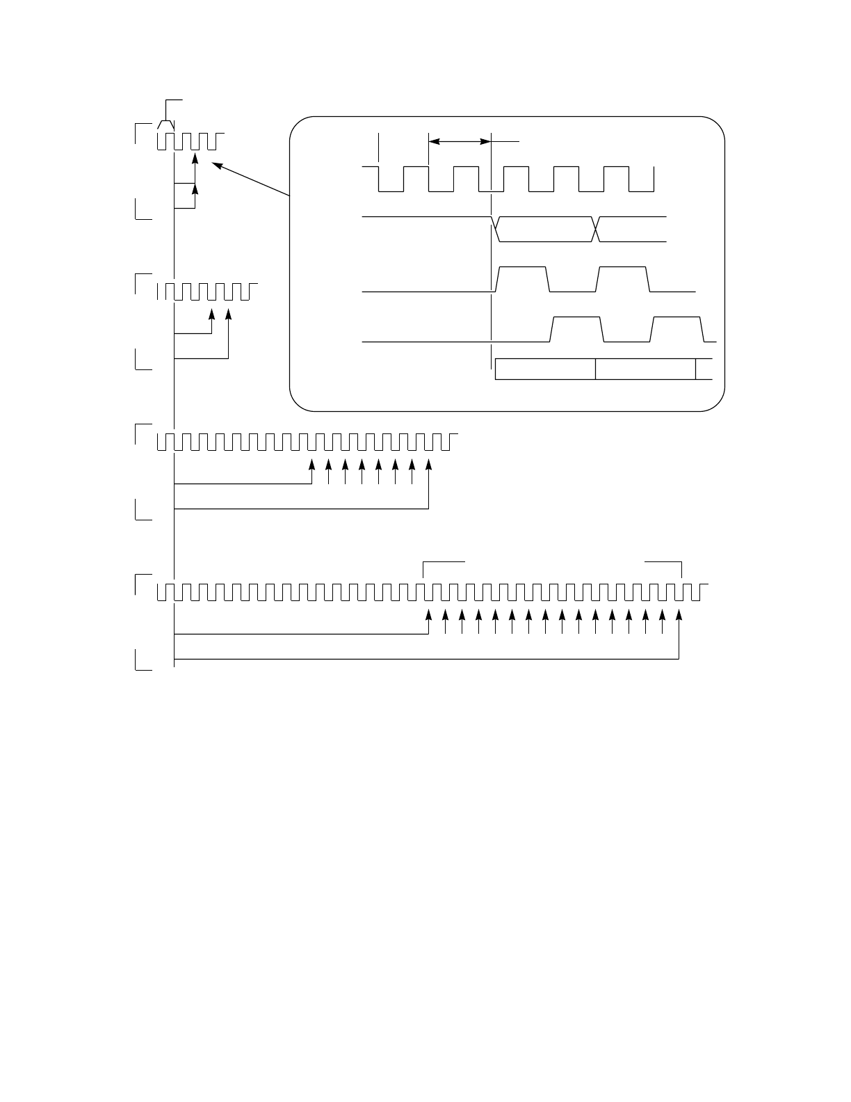
MOTOROLA SYNCHRONOUS SERIAL PERIPHERAL INTERFACE M68HC11
8-12 REFERENCE MANUAL
Figure 8-4 Delay from Write SPDR to Transfer Start (Master)
8.6.2 Transfer Ending Period
An SPI transfer is technically complete when the SPIF flag is set, but, depending on
the configuration of the SPI system, there may be additional tasks. Because the SPI
bit rate does not affect timing of the ending period, only the fastest rate will be consid-
ered in discussions of the ending period.
When the SPI is configured as a master, SPIF is set at the end of the eighth SCK cycle.
When CPHA equals one, SCK is inactive for the last half of the eighth SCK cycle. Fig-
ure 8-5 shows the transfer ending period for a master. The SCK waveforms in this fig-
ure show only the CPOL equals zero case, since clock polarity does not affect timing
of the ending period.
MIN
MAX
E CYCLE WHERE SPDR WRITTEN
MAX
MIN
MAX
MIN
MAX
SCK=E÷32 SCK=E÷16 SCK=E÷4 SCK=E÷2
SCK CYCLE
NUMBER
SCK
(CPHA=0)
SCK
(CPHA=1)
MOSI
E
WRITE
TO SPDR INITIATION DELAY
MSB BIT 6
12
INSET: Detailed view of initiation delay from write SPDR to transfer begin.
POSSIBLE TRANSFER START POINTS
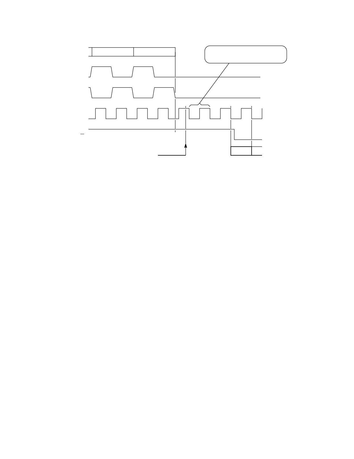
M68HC11 SYNCHRONOUS SERIAL PERIPHERAL INTERFACE MOTOROLA
REFERENCE MANUAL 8-13
Figure 8-5 Transfer Ending for an SPI Master
When the SPI is operating as a slave, the ending period is different because the SCK
line can be asynchronous to the MCU clocks of the slave and because the slave does
not have access to as much information about SCK cycles as the master. For exam-
ple, when CPHA equals one, where the last SCK edge occurs in the middle of the
eighth SCK cycle, the slave has no way of knowing when the end of the last SCK cycle
is. For these reasons, the slave considers the transfer complete after the last bit of se-
rial data has been sampled, which corresponds to the middle of the eighth SCK cycle.
A synchronization delay is required so the setting of the SPIF flag is properly posi-
tioned relative to the internal PH2 clock of the slave. Figure 8-6 shows the ending pe-
riod for a slave. The SCK waveforms in this figure show only the CPOL equals zero
case, since clock polarity does not affect timing of the ending period.
SCK CYCLE #
SCK (CPHA=0)
SCK (CPHA=1)
78
PC (LOW) PC (HIGH)
EARLIEST POSSIBLE STACKING
DUE TO SPIF INTERRUPT
(NO OTHER INTERRUPT PENDING)
SPIF SET
E
NEW OPCODE
(NOT EXECUTED DUE TO INTERRUPT)
R/W
•••
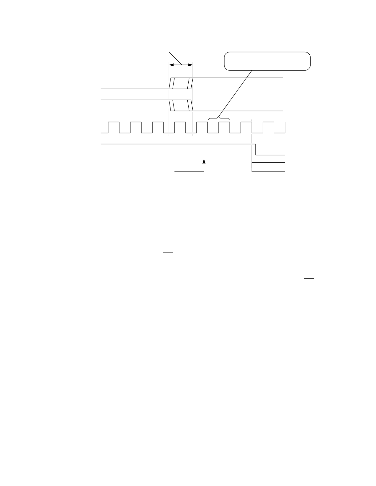
MOTOROLA SYNCHRONOUS SERIAL PERIPHERAL INTERFACE M68HC11
8-14 REFERENCE MANUAL
Figure 8-6 Transfer Ending for an SPI Slave
When CPHA equals zero, there is a potential problem that can be avoided by proper
software but is sometimes overlooked. The SPIF flag is set at the end of a transfer, but
the slave is not permitted to write new data to the SPDR while the SS line is still low.
If the master device is busy, the SS line to the slave can remain low longer than the
slave expects. The proper way for the slave to manage this problem is to read the state
of the port D bit 5 pin, (SS), before writing to SPDR. If this procedure is not followed
(slave mode and CPHA = 0) and an attempt is made to write to SPDR before SS goes
high, a write collision will result.
8.7 Transfers to Peripherals with Odd Word Lengths
The SPI system in the MC68HC11A8 is oriented toward 8-bit transfers, but not all pe-
ripherals use eight bits. Some peripherals use multiples of eight bits, but a few use odd
word lengths. When a peripheral uses an odd number of bits, it is usually possible to
send it some multiple of eight bits, and the peripheral will ignore the extra bits. Serial
peripherals are commonly designed for cascading. In these devices, only the most re-
cent bits received will be important, and extra leading bits pass through the peripheral.
In more unusual peripheral designs, the leading bits can alter the way the peripheral
will interpret the remaining bits in a serial stream. In all cases, the requirements of
each peripheral in the system must be considered.
The MC144110 six-channel, 6-bit, D/A converter peripheral is an example of a periph-
eral with an odd word length. This device requires six 6-bit words (a total of 36 bits) to
update all six channels. The following examples show two possible approaches for
managing this device to illustrate some of the possible trade-off decisions found in un-
SCK (CPHA=1)
LAST EDGE
SCK (CPHA=0)
SECOND LAST EDGE
PC (LOW) PC (HIGH)
EARLIEST POSSIBLE STACKING
DUE TO SPIF INTERRUPT
(NO OTHER INTERRUPT PENDING)
SPIF SET
E
NEW OPCODE
(NOT EXECUTED DUE TO INTERRUPT)
SYNCHRONIZATION
UNCERTAINTY
R/W
•••
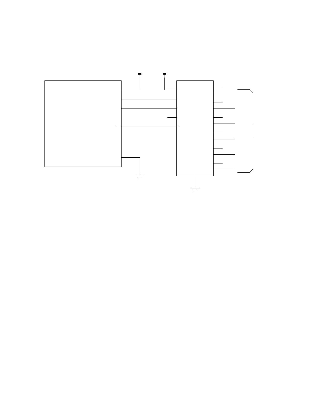
M68HC11 SYNCHRONOUS SERIAL PERIPHERAL INTERFACE MOTOROLA
REFERENCE MANUAL 8-15
usual peripherals. The hardware hookup, which is identical for both examples, is
shown in Figure 8-7. A software program includes the routines needed for both exam-
ples. Figure 8-8 shows the register definitions and RAM variables used by both exam-
ple programs.
Figure 8-7 Hardware Hookup for Examples 8–1 and 8–2
D
D
DD
V
MC68HC11EVB BOARD
3
2
5
4
7
17
12
11
14
13
16
15
R1
Q1
R2
Q2
R3
Q3
R4
Q4
R5
Q5
R6
Q6
MEASURE WITH
HIGH-IMPEDANCE
VOLTMETER
CLK
IN
OUT
1
10
18
8EN
MC144110 D/A
P1-26
P1-24
P1-23
P1-1
P1-25
CLK
PD3/MOSI
PD5/SS
VSS
NOTE: Pin numbers on P1 of the MC68HC11EVB board are the same as those for a 52-pin MC68HC11A8.
DD
V
DD
VDD
V
VSS
6

MOTOROLA SYNCHRONOUS SERIAL PERIPHERAL INTERFACE M68HC11
8-16 REFERENCE MANUAL
* Register definitions for 68HCll registers (used for Ex 8-1 & 8-2)
1008 PORTD EQU $1008 Port D data register
* " - , - ,SS* ,SCK ;MOSI,MISO,TxD ,RxD "
1009 DDRD EQU $1009 Port D data direction
1028 SPCR EQU $1028 SPI control register
* "SPIE,SPE ,DWOM,MSTR;CPOL,CPHA,SPR1,SPR0"
1029 SPSR EQU $1029 SPI status register
* "SPIF,WCOL, - ,MODF; - , - , - , - "
102a SPDR EQU $102A SPI data register; Read-Buffer; Write-Shifter
* RAM variables (DAx used by Ex 8-1 & 8-2, SPIx used only by 8-1)
0000 DA1 EQU $00 6-bit val for D/A ch 1 "-,-,15,14;13,12,11,10"
0001 DA2 EQU $01 6-bit val for D/A ch 2 "-,-,25,24;23,22,21,20"
0002 DA3 EQU $02 6-bit val for D/A ch 3 "-,-,35,34;33,32,31,30"
0003 DA4 EQU $03 6-bit val for D/A ch 4 "-,-,45,44;43,42,41,40"
0004 DA5 EQU $04 6-bit val for D/A ch 5 "-,-,55,54;53,52,51,50"
0005 DA6 EQU $05 6-bit val for D/A ch 6 "-,-,65,64;63,62,61,60"
* Upper 2 bits of DAx should be 0 but will be ignored.
0006 SPI1 EQU $06 SPI packed byte 1 "--,--,--,--;65,64,63,62"
0007 SPI2 EQU $07 SPI packed byte 2 "61,60,55,54;53,52,51,50"
0008 SPI3 EQU $08 SPI packed byte 3 "45,44,43,42;41,40,35,34"
0009 SPI4 EQU $09 SPI packed byte 4 "33,32,31,30;25,24,23,22"
000a SPI5 EQU $0A SPI packed byte 5 "21,20,15,14;13,12,11,10"
* NOTE: Upper 4 bits of SPI1 are unused extras but will be 0.
Figure 8-8 Register Definitions and RAM Variables for Examples 8–1 and 8–2
8.7.1 Example 8–1: On-Chip SPI Driving an MC144110 D/A
In this example, software must reformat (pack) the six 6-bit data values into five 8-bit
words, which can then be transferred to the MC144110 D/A using the on-chip SPI. Fig-
ure 8-9 is the software listing for the Example 8–1 routines.
In the Example 8–1 setup, the MCU is running at 2-MHz E-clock frequency. To meet
the timing requirements of the MC144110 D/A, the slowest SPI clock rate (E÷32) is
used. Figure 8-10 shows a detailed analysis of important timing parameters. These
timing details are derived from knowledge of the cycle-by-cycle activity of software in-
structions and detailed SPI system timing. This timing analysis depicts the strong in-
terdependence of software and hardware in MCU systems.
8.7.2 Example 8–2: Software SPI Driving an MC144110 D/A
Sometimes it is easier and/or more efficient to use software to emulate an SPI to allow
even more flexibility than the on-chip SPI system allows (e.g., odd word lengths). As
Example 8–2 shows, it is not necessarily difficult to manipulate I/O pins to create an
SPI-like interface. In this example, a software SPI allows 6-bit transfers so the six D/A
values can be used without any packing or reformatting (needed in the previous ex-
ample). Figure 8-11 is the software listing for Example 8–2.

M68HC11 SYNCHRONOUS SERIAL PERIPHERAL INTERFACE MOTOROLA
REFERENCE MANUAL 8-17
**********************************************************************
* Example 8-1 *
* This example program uses the on-chip hardware SPI to drive an *
* MC144110 six channel D to A converter peripheral. *
* To try Ex 8-1, connect MC144110 to Port D pins on EVB, load *
* program into EVB RAM, manually enter data for DA1 to DA6 and *
* execute a GO to $COOO. *
*********************************************************************
c000 ORG $C000 Start of user’s RAM in EVB
c000 Be cf ff [3] INIT1 LDS #$CFFF Top of C page RAM
c003 86 2f [2] LDAA #$2F
* SS*-Hi, SCK-Lo, MOSI-Hi
c005 b7 10 08 [4] STAA PORTD So SS* stays high when DDRD5 set
c008 86 38 [2] LDAA #$38 -,-,1,1;1,0,0,0
c00a b7 10 09 [4) STAA DDRD SS*, SCK, MOSI - Outs
* MISO, TxD, RxD - Ins
* DDRD5=1 so SS* pin is a general-purpose output
c00d 86 57 [2] LDAA #$57
c00f b7 10 28 [4] STAA SPCR SPI on as Master, CPHA=1, CPOL=0
* E/32 Clk rate
***
* Following two instructions call main routine for Ex 8-1
***
c012 8d 38 [6] BSR UPDAT1 Xfer 5 8-bit words to MC144110
c014 7e e0 00 [3] JMP $E000 Restart BUFFALO
***
c04c 3c [4] UPDAT1 PSHX Save registers X and A
c04d 18 3c [5] PSHY
c04f 36 [3] PSHA
c050 8d c5 [6] BSR REFORM Reformat data so SPI can xfer it
c052 ce 00 06 [3] LDX #SPI1 Point at 1st byte to send via SPI
c055 18 ce 10 00[4] LDY #$1000 Point at on-chip registers
c059 18 1d 08 20[8] BCLR PORTD,Y %00100000 Drive SS* low
c05d a6 00 [4] TFRLP1 LDAA 0,X Get a byte to transfer via SPI
c05f b7 10 2a [4] STAA SPDR Write SPI data reg to start xfer
c062 b6 10 29 [4] WAIT1 LDAA SPSR Loop to wait for SPIF
c065 2a fb [3] BPL WAIT1 SPIF is in MSB of SPSR
* (when SPIF set, SPSR neg)
c067 08 [3] INX Point to next SPI byte
c068 0c 00 0b [4] CPX #SPI5+1 Done yet ?
c06b 26 f0 [3] BNE TFRLP1 If not, tfr another byte
c06d 18 1c 08 20[8] BSET PORTD,Y %00100000 Drive SS* high
c071 32 [4] PULA When done, restore regs X, Y & A
c072 18 38 [6] PULY
c074 38 [5] PULX
c075 39 [5] RTS ** Return **
Figure 8-9 Example 8–1 Software Listing (Sheet 1 of 2)

MOTOROLA SYNCHRONOUS SERIAL PERIPHERAL INTERFACE M68HC11
8-18 REFERENCE MANUAL
********************************************************************************
* REFORM - This subroutine reformats six 6-bit values into five 8-bit *
* values so they can be sent by the SPI system. *
* *
* The MC144110 needs 36 bits of information, which is not a multiple *
* of 8 bits; however, we can send five 8 bit words (40 bits) and the *
* MC144110 will use only the last 36 bits. *
* *
* Original format Change to this format *
* DA1 "-,-,15,14;13,12,11,10" SPI1 "--,--,--,--;65,64,63,62" *
* DA2 "-,-,25,24;23,22,21,20" SPI2 "61,60,55,54;53,52,51,50" *
* DA3 "-,-,35,34;33,32,31,30" SPI3 "45,44,43,42;41,40,35,34" *
* DA4 "-,-,45,44;43,42,41,40" SPI4 "33,32,31,30;25,24,23,22" *
* DA5 "-,-,55,54;53,52,51,50" SPI5 "21,20,15,14;13,12,11,10" *
* DA6 "-,-,65,64;63,62,61,60 *
********************************************************************************
c017 37 [3] REFORM PSHB Save registers B and A
c018 36 [3] PSHA
c019 96 00 [3] IDAA DA1 A="--,--,15,14;13,12,11,10"
c01b 48 [2] ASLA A="--,15,14,13;12,11,10, 0"
c01c 48 [2] ASLA A="15,14,13,12;11,10, 0, 0"
c01d d6 01 [3] LDAB DA2 B="--,--,25,24;23,22,21,20"
c01f c4 3f [2] ANDB #$3F B=" 0, 0,25,24;23,22,21,20"
c021 54 [2] LSRB B=" 0, 0, 0,25;24,23,22,21" C="20
c022 46 [2] RORA A="20,15,14,13;12,11,10, 0"
c023 54 [2] LSRB B=" 0, 0, 0, 0;25,24,23,22" C="21
c024 46 [2] RORA A="21,20,15,14;13,12,11,10"
c025 97 0a [3] STAA SPI5 SPI5 is done
c027 d7 09 [3] STAB SPI4 SPI4 intermediate value
c029 96 03 [3] LDAA DA4 A="--,--,45,44;43,42,41,40"
c02b d6 02 [3] LDAB DA3 B="--,--,35,34;33,32,31,30"
c02d 58 [2] ASLB B="--,35,34,33;32,31,30, 0"
c02e 58 [2] ASLB B="35,34,33,32;31,30, 0, 0"
c02f 58 [2] ASLB B="34,33,32,31;30, 0, 0, 0" C="35
c030 49 [2] ROLA A="--,45,44,43;42,41,40,35"
c031 58 [2] ASLB B="33,32,31,30; 0, 0, 0, 0" C="34
c032 49 [2] ROLA A="45,44,43,42;41,40,35,34"
c033 da 09 [3] ORAB SPI4 B="33,32,31,30;25,24,23,22"
c035 d7 09 [3] STAB SPI4 SPI4 now complete
c037 97 08 [3] STAA SPI3 SPI3 done
c039 96 04 [3] LDAA DA5 A="--,--,55,54;53,52,51,50"
c03b 48 [2] ASLA A="--,55,54,53;52,51,50, 0"
c03c 48 [2] ASLA A="55,54,53,52;51,50, 0, 0"
c03d d6 05 [3] LDAB DA6 B="--,--,65,64;63,62,61,60"
c03f c4 3f [2] ANDB #$3F B=" 0, 0,65,64;63,62,61,60"
c041 54 [2] LSRB B=" 0, 0, 0,65;64,63,62,61" C="60
c042 46 [2] RORA A="60,55,54,53;52,51,50, 0"
c043 54 [2] LSRB B=" 0, 0, 0, 0;65,64,63,62" C="61
c044 46 [2] RORA A="61,60,55,54;53,52,51,50"
c045 97 07 [3] STAA SPI2 SPI2 done
c047 d7 06 [3] STAB SPI1 SPI1 done
c049 32 [4] PULA Restore registers A and B
c04a 33 [4] PULB
c04b 39 [5] RTS ** Return **
Figure 8-9 Example 8–1 Software Listing (Sheet 2 of 2)
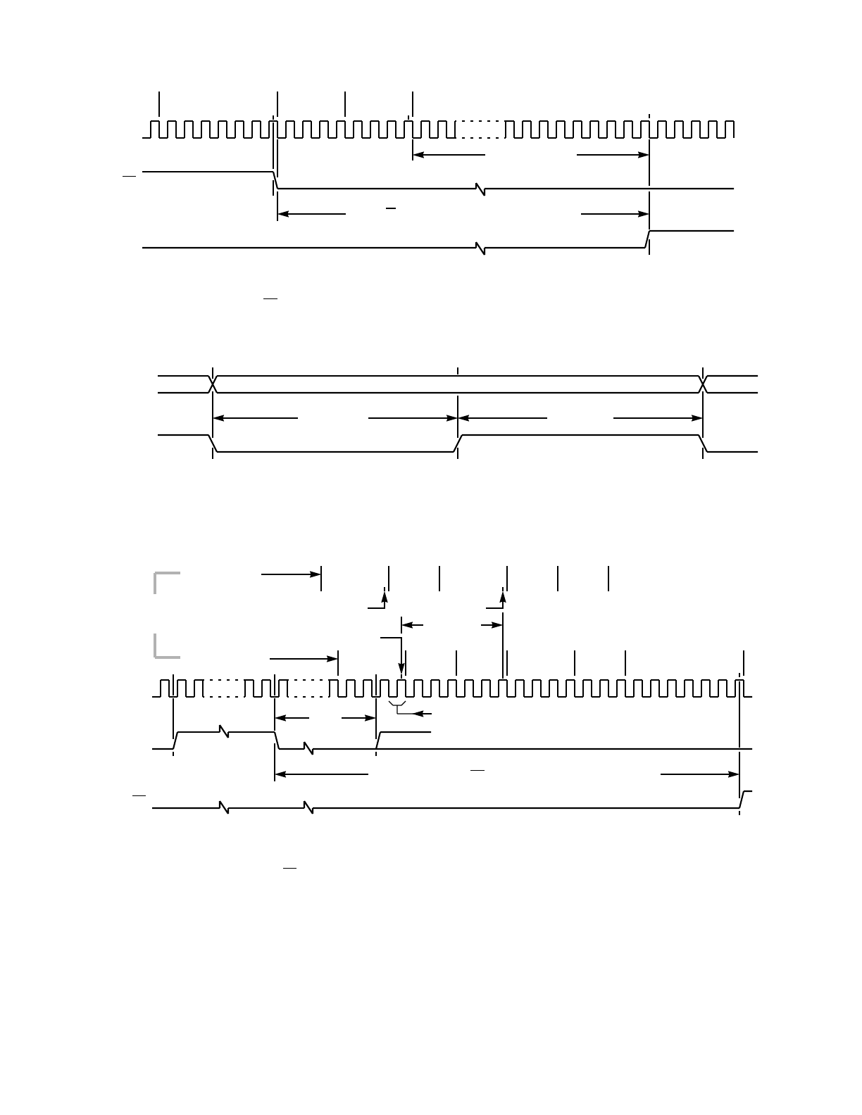
M68HC11 SYNCHRONOUS SERIAL PERIPHERAL INTERFACE MOTOROLA
REFERENCE MANUAL 8-19
Figure 8-10 Timing Analysis for Example 8–1
6 E CYCLES
DELAY; EN LOW TO CLK (MIN 11.5 µS/MAX 19.5 µS)
E
LDAA 0,X
15 TO 31 E CYCLES
(SEE FIGURE 8-4)
a) EN low to clock start delay (MC144110 needs 5 µS)
BNE
TFRLP1
c) Last SCK edge to EN release timing (MC144110 needs 5 µS)
b) Data valid vs. clock timing (MC144110 needs 1 µS setup/ 5 µS hold)
CPX #SP15+1
BCLR PORTD,X $20 STAA SPDR
EN
SCK
LAST SCK EDGE TO EN RELEASE (MIN 19.5 µS/MAX 22.5 µS)
E
LDAA SPSR
EARLIEST READ OF SPIF = 1
SCK
SS
~8µS SETUP
MOSI
SCK
VALID DATA
~8µS HOLD
BSET PORTD,X $40INX
BPL
WAIT1
• • •LDAA SPSR INX
BPL
WAIT1
LDAA SPSR BPL
WAIT1
SPIF NOT SET YET SPIF SET NOW
SPIF SET NOW
(REFER TO FIGURE 8-5 FOR SPI TRANSFER ENDING DETAILS)
LONGEST CASE
SHORTEST CASE
(VARIES WITH SCK
ALIGNMENT TO
SOFTWARE)
~8µS

MOTOROLA SYNCHRONOUS SERIAL PERIPHERAL INTERFACE M68HC11
8-20 REFERENCE MANUAL
****************************************************************************
* Example 8-2 *
* *
* This example program uses a software equivalent of the SPI to *
* drive an MC144110 six channel D to A converter peripheral. The *
* physical hookup is the same as that of the previous example to make *
* comparisons easier. *
* *
* To try Ex 8-2, connect MC144110 to Port D pins on EVB, load *
* program into EVB RAM, manually enter data for DA1 to DA6 and *
* execute a GO to $CI00 *
****************************************************************************
c100 ORG $C100
c100 8e cf ff [3] INIT2 LDS #$CFFF Top of C page RAM
c103 86 2f [2] LDAA #$2F -,-,1,0;1,1,1,1
c105 b7 10 08 [4] STAA PORTD PD5/SS*-Lo,PD4/SCK-Lo,PD3/MOSI-Hi
c108 86 38 [2] LDAA #$38 -,-,1,1;1,0,0,0
c10a b7 10 09 [4] STAA DDRD PD5, PD4, PD3 =Outs; Others =Ins
c10d 86 04 [2] LDAA #$04
* "SPIE,SPE,DWOM,MSTR;CPOL,CPHA,SPR1,SPR0"
c10f b7 10 28 [4] STAA SPCR Make sure SPI off
***
* Following two instructions call main routine for Ex 8-2
***
c112 8d 03 [6] BSR UPDAT2 Xfer six 6 bit words to MC144110
c114 7e e0 00 [3] JMP $E000 Restart BUFFALO
***
c117 3c [4] UPDAT2 PSHX Save X, Y and A
c118 18 3c [5] PSHY
c11a 36 [3] PSHA
c11b 18 ce 00 05[4] LDY #DA6 Point at 1st D/A value to xfer.
c11f ce 10 00 [3] LDX #$1000 Point at register area.
c122 86 20 [2] TFRLP2 LDAA #$20 1st pntr to MSB of 6 bit data val
c124 1d 08 20 [7] BCLR PORTD,X %00100000 PD5(SS*) Falling edge
c127 01 [2] NOP Need more dly for MC144110 specs.
c128 01 [2] NOP
c129 1c 08 10 [7] NXTBIT BSET PORTD,X %00010000 PD4(SCK) Rising edge
c12c 18 a5 00 [5] BITA 0,Y Test sense of bit to be sent
c12f 27 05 [3] BEQ ZBIT If zero skip around
c131 1c 08 08 [7] BSET PORTD,X %00001000 PD3(MOSI) Hi bit
c134 20 05 [3] BRA ENDBIT
c136 1d 08 08 [7] ZBIT BCLR PORTD,X %00001000 PD3(MOSI) Lo bit
c139 20 00 [3] BRA ENDBIT Want Lo time to match Hi time
c13b 1d 08 10 [7] ENDBIT BCLR PORTD,X %00010000 PD4(SCK) Falling edge
c13e 44 [2] LSRA Pointer to nxt lower bit position
c13f 26 e8 [3] BNE NXTBIT Done if pointer shifted past LSB
c141 18 09 [4] DEY Point at next value to send
c143 18 8c ff ff[5] CPY #DA1-1 Done yet?
c147 26 db [3] BNE TFRLP2 If not go back to top of loop
c149 1c 08 20 [7] BSET PORTD,X %00100000 PD5(SS*) Rising edge
c14c 32 [4] PULA Restore X, Y and A
c14d 18 38 [6] PULY
c14f 38 [5] PULX
c150 39 [5] RTS ** RETURN **
Figure 8-11 Example 8–2 Software Listing
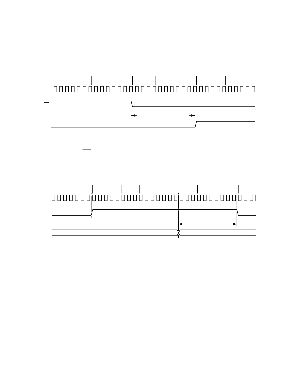
M68HC11 SYNCHRONOUS SERIAL PERIPHERAL INTERFACE MOTOROLA
REFERENCE MANUAL 8-21
Figure 8-12 shows a detailed analysis of important timing parameters. These timing
details are derived from knowledge of the cycle-by-cycle activity of software instruc-
tions. This timing analysis illustrates the strong interdependence of software and hard-
ware in MCU systems.
(a) EN Low to SCK Start Delay (MC144110 Needs 5 µs)
(b) Data to SCK Setup (MC144110 Needs 1 µs)
Figure 8-12 Timing Analysis for Example 8–2 (Sheet 1 of 2)
DELAY; EN LOW TO CLK (5.5 µS)
E
NOP
BCLR PORTD,X $20 BITA 0,Y
EN
SCK
• • •NOP BSET PORTD,X $10
~5µS SETUP
E
BRA
ENDBIT
BSET PORTD,X $10
SCK
MOSI
• • •
BSET PORTD,X $08 BCLR PORTD,X $10
BCLR PORTD,X $08
BEQ
ZBIT
BITA 0,Y
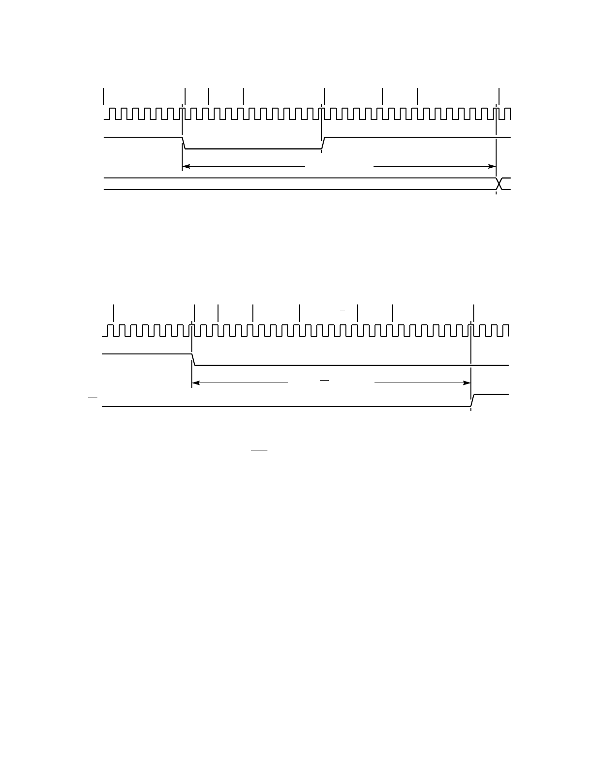
MOTOROLA SYNCHRONOUS SERIAL PERIPHERAL INTERFACE M68HC11
8-22 REFERENCE MANUAL
(c) Data Hold vs. SCK (MC144110 Needs 5 µs)
(d) SCK Low to EN Hold (MC144110 Needs 5 µs)
Figure 8-12 Timing Analysis for Example 8-2 (Sheet 2 of 2)
DATA HOLD (13.5 µS)
E
LSRA
BCLR PORTD,X $10
SCK
MOSI
BITA 0,YBSET PORTD,X $10 BEQ
ZBIT BSET PORTD,X $08
BCLR PORTD,X $08
BNE
NXTBIT
SCK TO EN HOLD (12 µS)
E
CPY #DA1 1BCLR PORTD,X $10
SCK
EN
BNE
TFRLP2 BSET PORTD,X $20LSRA BNE
NXTBIT DEY

M68HC11 ASYNCHRONOUS SERIAL COMMUNICATIONS INTERFACE MOTOROLA
REFERENCE MANUAL 9-1
SECTION 9
ASYNCHRONOUS SERIAL COMMUNICATIONS INTERFACE
This section describes the universal asynchronous receiver transmitter (UART) type
serial communications interface (SCI) system, which is one of two independent serial
I/O subsystems in the M68HC11. The other serial I/O subsystem (called SPI) provides
for high-speed synchronous serial communication to peripherals or other microcontrol-
ler units (MCUs), usually located on the same printed circuit board as the M68HC11.
This SCI system can be used to connect a CRT terminal or personal computer to the
MCU, or several widely distributed MCUs can use their SCI subsystems to form a se-
rial communication network.
9.1 General Description
The SCI is a full-duplex UART-type asynchronous system, using standard non-return-
to-zero (NRZ) format (one start bit, eight or nine data bits, and a stop bit). An on-chip
baud rate generator derives standard baud-rate frequencies from the MCU oscillator.
Both the transmitter and the receiver are double buffered; thus, back-to-back charac-
ters can be handled easily, even if the central processing unit (CPU) is delayed in re-
sponding to the completion of an individual character. The SCI transmitter and
receiver are functionally independent but use the same data format and baud rate. In
this reference manual, baud rate and bit rate are used synonymously. The user will
usually have to provide external level-shifter buffers to translate the RS232 or RS422
levels (typically ± 12 V) to the 0- to 5-V logic levels used by the MCU.
This SCI receiver includes a number of advanced features to assure high-reliability
data reception and to assist development of efficient communications networks. The
M68HC11 resynchronizes the receiver bit clock on all one-to-zero transitions in the bit
stream rather than just at the beginning of the start bit time; therefore, differences in
baud rate between the sending device and the MCU are not as likely to cause recep-
tion errors. Three logic-level samples are taken near the middle of each bit time, and
majority logic decides the sense for the bit. Even if noise causes one of these samples
to be incorrect, the bit will still be received correctly. The receiver also has the ability
to enter a temporary standby mode (called receiver wake up) to ignore messages in-
tended for a different receiver. Logic automatically wakes up the receiver in time to see
the first character of the next message. This wake-up feature greatly reduces CPU
overhead in multi-drop SCI networks.
The SCI transmitter can produce queued characters of idle (whole characters of all
logic one) and break (whole characters of all logic zero). In addition to the usual trans-
mit data register empty (TDRE) status flag, this SCI also provides a transmit complete
(TC) indication that can be used in applications with a modem.
9.1.1 Transmitter Block Diagram
Figure 9-1 is a block diagram of the transmitter section of the SCI subsystem. The de-
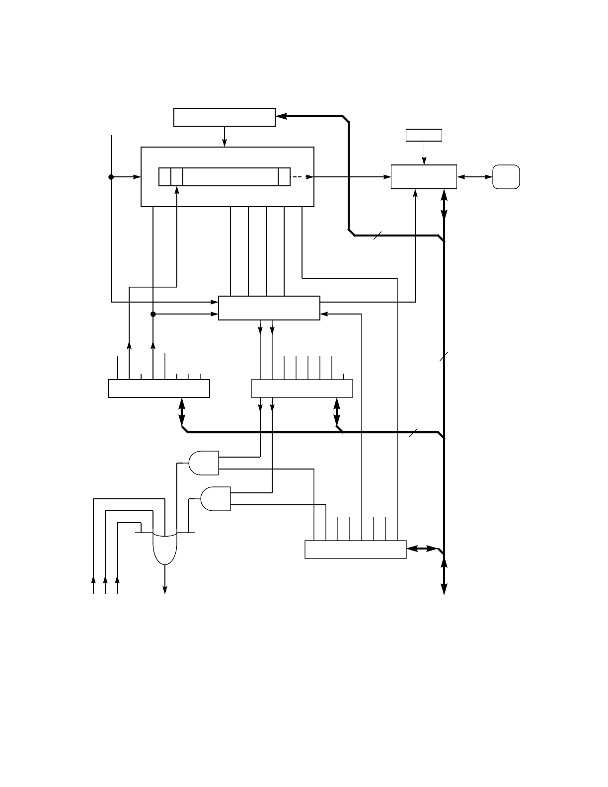
MOTOROLA ASYNCHRONOUS SERIAL COMMUNICATIONS INTERFACE M68HC11
9-2 REFERENCE MANUAL
scription given in the following paragraphs is an overview; a more detailed discussion
of the SCI transmitter is given in 9.3 SCI Transmitter.
Figure 9-1 SCI Transmitter Block Diagram
The heart of the transmitter is the transmit serial shift register near the top of the figure.
Usually, this shift register gets its data from the write-only transmit buffer. Data gets
FE
NF
OR
IDLE
RDRF
TC
TDRE
SCSR INTERRUPT STATUS
SBK
RWU
RE
TE
ILIE
RIE
TCIE
TIE
SCCR2 SCI CONTROL 2
TRANSMITTER
CONTROL LOGIC
TCIE
TC
TIE
TDRE
SCI Rx
REQUESTS
SCI INTERRUPT
REQUEST
INTERNAL
DATA BUS
PIN BUFFER
AND CONTROL
H(8)76543210L
10 (11) - BIT Tx SHIFT REGISTER
DDD1
PD1
TxD
SCDR Tx BUFFER
TRANSFER Tx BUFFER
SHIFT ENABLE
JAM ENABLE
PREAMBLE—JAM 1s
BREAK—JAM 0s
(WRITE ONLY)
FORCE PIN
DIRECTION (OUT)
SIZE 8/9
WAKE
M
T8
R8
SCCR1 SCI CONTROL 1
TRANSMITTER
BAUD RATE
CLOCK
8
8
8

M68HC11 ASYNCHRONOUS SERIAL COMMUNICATIONS INTERFACE MOTOROLA
REFERENCE MANUAL 9-3
into the transmit buffer when software writes to the SCI data register (SCDR). When-
ever data is transferred into the shifter from the transmit buffer, a zero is loaded into
the least significant bit (LSB) of the shifter to act as a start bit, and a logic one is loaded
into the last bit position to act as a stop bit. In the case of a preamble, the shifter is
jammed to all ones, including the bit position usually holding the logic zero start bit. A
preamble is jammed each time the transmit enable bit is written from zero to one. In
the case of a send break command, the shifter is jammed to all zeros, including the
last bit position usually holding the logic one stop bit.
The T8 bit in SCI control register 1 (SCCR1) acts like an extra high-order bit (ninth bit)
of the transmit buffer register. This ninth bit is only used if the M bit in SCCR1 is one
to select the 9-bit data character format. The M bit also controls the length of idle and
break characters. The R8 and WAKE bits in SCCR1 are associated with the SCI re-
ceiver and are only shown in Figure 9-1 for reference.
The pin buffer logic is quite flexible and useful in some SCI systems. This block
diagram is not detailed enough to show all of the functions of this block. 9.3.6 TxD Pin
Buffer Logic describes this logic in greater detail, and a complete MOS transistor-lev-
el schematic and explanation of this logic is included in 7.3.6.2 PD1 (TxD) Pin Logic.
The status flag and interrupt generation logic is shown in Figure 9-1. The TDRE and
TC status flags in the SCI status register (SCSR) are automatically set by the trans-
mitter logic. These two bits can be read at any time by software. The transmit interrupt
enable (TIE) and transmit complete interrupt enable (TCIE) interrupt control bits en-
able the TDRE and TC bits, respectively, to generate SCI interrupt requests.
9.1.2 Receiver Block Diagram
Figure 9-2 is a block diagram of the receiver section of the SCI subsystem. The de-
scription given in the following paragraphs is an overview; a more detailed discussion
of the SCI receiver is given in 9.4 SCI Receiver.
SCI receive data comes in the RxD pin, is buffered, and drives the data recovery block.
The data recovery block is actually a high-speed shifter operating at 16 times the bit
rate; whereas, the main-receive serial shifter operates at one times the bit rate. This
higher speed sample rate allows the start-bit leading edge to be located more accu-
rately thana1xclock would allow. The high-speed clock also allows several samples
to be taken within a bit time so logic can make an intelligent decision about the logic
sense of a bit (even in the presence of noise). The data recovery block provides the
bit level to the main receiver shift register and also provides a noise flag status indica-
tion.
This block diagram is not detailed enough to show all of the subtleties of the RxD pin
buffer logic; a complete schematic and explanation of this pin logic can be found in
7.3.6.1 PD0 (RxD) Pin Logic.
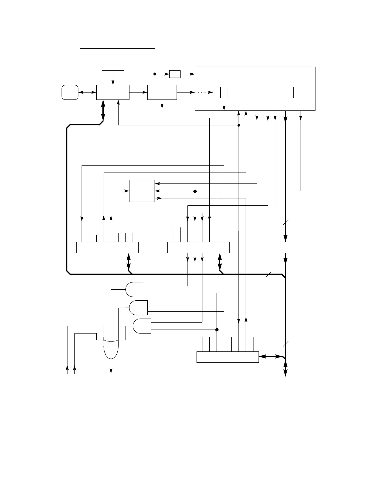
MOTOROLA ASYNCHRONOUS SERIAL COMMUNICATIONS INTERFACE M68HC11
9-4 REFERENCE MANUAL
Figure 9-2 SCI Receiver Block Diagram
The heart of the receiver is the receive serial shift register shown in Figure 9-2. This
FE
NF
OR
IDLE
RDRF
TC
TDRE
SCSR SCI STATUS 1
SBK
RWU
RE
TE
ILIE
RIE
TCIE
TIE
SCCR2 SCI CONTROL 2
WAKE
M
T8
R8
WAKEUP
LOGIC
RIE
OR
ILIE
IDLE
SCI Tx
REQUESTS
SCI INTERRUPT
REQUEST INTERNAL
DATA BUS
PIN BUFFER
AND CONTROL
DDD0
PD0
RxD
SCDR Rx BUFFER
STOP
(8)76543210
10 (11) - BIT
Rx SHIFT REGISTER
(READ ONLY)
SCCR1 SCI CONTROL 1
RIE
RDRF
START
MSB ALL ONES
DATA
RECOVERY
÷16
RWU
RE
M
DISABLE
DRIVER
RECEIVER
BAUD RATE
CLOCK
8
8
8

M68HC11 ASYNCHRONOUS SERIAL COMMUNICATIONS INTERFACE MOTOROLA
REFERENCE MANUAL 9-5
shifter is enabled by the receive enable (RE) bit from the SCI control register 2
(SCCR2). The M bit from the SCCR1 register determines whether the shifter will be 10
or 11 bits long. After detecting the stop bit of a character, the received data is trans-
ferred from the shifter to the SCDR, and the receive data register full (RDRF) status
flag is set. When a character is ready to be transferred to the receive buffer but the
previous character has not yet been read, an overrun condition occurs. In the overrun
condition, data is not transferred and the overrun (OR) status flag is set to indicate the
error.
The wake-up block uses the WAKE control bit from SCCR1 to decide whether to use
the most significant bit (MSB) signal (address mark) or the ALL ONES signal (idle line)
to wake up the receiver. When the selected condition is detected, the wake-up logic
clears the receiver wake-up (RWU) bit in SCCR2, which wakes up the receiver.
There are three receiver-related interrupt sources in the SCI. These flags can be
polled by software or optionally cause an SCI interrupt request. The receive interrupt
enable (RIE) control bit enables the RDRF and the OR status flags to generate hard-
ware interrupt requests. The idle line interrupt enable (ILIE) control bit allows the IDLE
status flag to generate SCI interrupt requests.
9.2 SCI Registers and Control Bits
Primarily, the SCI system is configured and controlled by five registers (BAUD,
SCCR1, SCCR2, SCSR, and SCDR). In addition, the port D register, data direction
register for port D (DDRD), and the port D wired-OR mode bit in the SPI control regis-
ter (SPCR) are secondarily related to the SCI system. First, the main function of each
of these registers is presented, and then detailed descriptions of each bit are present-
ed.
When the SCI receiver and/or transmitter is enabled, the SCI logic takes control of the
pin buffers for the associated port D pin(s). Data directions for the RxD and TxD pins
are overridden to input and output, respectively. Even though it does not control the
direction of port D pins while the SCI has control, the DDRD can be important to a user
because it influences what will be read when port D is read by software. The DDRD
also determines how the pin will behave when the SCI gives up control. The port D
register is important to an SCI user because the value written to port D can determine
what will be driven out of port D when the SCI gives up control.
The port D wired-OR mode bit in the SPCR modifies the driver functions of port D pins,
even if they are being used for SCI or SPI functions.
The baud-rate control register (BAUD) is used to select the baud rate for SCI opera-
tions and contains two control bits for factory testing.
SCCR1 includes three bits associated with the optional 9-bit data format. The WAKE
bit is used to select one of two methods of receiver wake up.
SCCR2 contains the main SCI controls. The upper four bits are local interrupt enable
controls, which determine whether SCI status flags will be polled or will generate hard-
ware interrupt requests. The TE and RE bits are the respective transmitter and receiv-

MOTOROLA ASYNCHRONOUS SERIAL COMMUNICATIONS INTERFACE M68HC11
9-6 REFERENCE MANUAL
er subsystem enable controls. The RWU bit allows software to put the receiver to sleep
and hardware to automatically wake it up by clearing this bit. The send break SBK bit
allows software to generate break characters on the TxD line.
The SCSR contains two transmitter status flags and five receiver-related status flags.
The transmitter generates flags for TDRE and TC. The receiver generates flags for
RDRF, OR, idle-line detect (IDLE), a noise flag (NF), and a framing error (FE) indica-
tion.
The SCDR is actually two separate registers. TDR is a write-only transmit data buffer
register, and RDR is a read-only receive data buffer register. When software reads
SCDR, it is accessing RDR; when software writes to SCDR, it is accessing TDR.
9.2.1 Port D Related Registers and Control Bits (PORTD, DDRD, SPCR)
The following registers are the port D related registers. Because the SCI system uses
the two LSBs of this port, only the interactions between general-purpose I/O and the
use of these pins by the SCI will be discussed. The actual MOS logic for port D pins is
shown and discussed in 7.3.6 Port D.
Each internal peripheral subsystem interacts with port I/O pins in different ways. In
some cases, such as the SCI system, the internal subsystem overrides other pin con-
trols to actively take charge of the pin. In other cases, such as the SPI and pulse ac-
cumulator, the pin controls (data direction and others) still influence the configuration
of the pin logic. The user must never assume that all pins in a port are affected in the
same way by data direction controls.
When the SCI receiver is enabled (by the RE bit in the SCCR2 register), bit 0 of DDRD
is overridden, and the output buffer is disabled. Writes to port D bit 0 while the SCI has
control of the pin do not alter the logic state at the pin; however, any value written is
remembered in an internal latch. If the SCI receiver later relinquishes control of the pin,
the logic value in this latch will drive the PD0/RxD pin. Although the DDRD0 bit does
not affect the pin while the SCI receiver is enabled, it still affects what is returned when
port D is read. If DDRD0 is zero, the pin is read. If DDRD0 is one (suggesting the pin
should be an output), the value in the internal port D bit 0 latch is returned.
Bit 7 6 5 4 3 2 1 Bit 0
RESET: 0 0 0 0 0 0 0 0
REFER-
ENCE: — — PD5/SS PD4/SCK PD3/
MOSI PD2/
MISO PD1/TxD PD0/RxD
$1009 0 0 DDRD5 DDRD4 DDRD3 DDRD2 DDRD1 DDRD0 DDRD
RESET: 0 0 0 0 0 0 0 0
$1028 SPIE SPE DWOM MSTR CPOL CPHA SPR1 SPR0 SPCR
RESET: 0 0 0 0 0 1 U U

M68HC11 ASYNCHRONOUS SERIAL COMMUNICATIONS INTERFACE MOTOROLA
REFERENCE MANUAL 9-7
When the SCI transmitter is active, bit 1 of DDRD is overridden, and the corresponding
output buffer is forced on and is driven by SCI logic (as opposed to port output logic).
The transmitter is active (controlling the PD1/TxD pin) whenever the transmitter en-
able bit (TE in the SCCR2 register) is one or an unfinished character is being transmit-
ted after the TE bit is disabled. Writes to bit 1 of port D while the SCI has control of the
pin do not alter the logic state at the pin; however, any value written is remembered in
an internal latch. If the SCI transmitter later relinquishes control of the pin, the logic
value in this latch will drive the PD1/TxD pin. Although the DDRD1 bit does not affect
the pin while the SCI transmitter is active, it still affects what is returned when port D
is read. If DDRD1 is zero, the pin is read (reflects what the SCI transmitter is currently
driving out of the pin). If DDRD1 is one (suggesting the pin should be an output), the
value in the internal port D bit 1 latch is returned (reflects what the pin would revert to
if the SCI transmitter relinquishes control of the pin).
All six bits of port D are affected by the port D wired-OR mode control bit (DWOM in
the SPCR). Whenever DWOM is one, the high-side driver (P-channel device) for all
port D pins is disabled. This disabling makes port D pins behave somewhat like open-
collector outputs; thus, an external pull-up resistor is needed for any port D pin being
used as an output (general-purpose or peripheral subsystem outputs). The DWOM bit
does not affect the use of port D pins as inputs.
9.2.2 Baud-Rate Control Register (BAUD)
The following register and paragraphs describe the BAUD control register, which is
used to set the bit rate for the SCI system. Normally, this register is written once during
initialization to set the baud rate for SCI communications. Both the receiver and the
transmitter use the same baud rate, which is derived from the MCU bus rate clock. A
two-stage divider is used to develop customary baud rates from normal MCU crystal
frequencies; therefore, it is not necessary to use special baud-rate crystal frequencies.
Table 9-1 and Table 9-2 should be adequate for most users, but a more comprehen-
sive tabulation of baud rates is provided in Table 9-3 to help users with unusual re-
quirements.
TCLR — Clear Baud-Rate Timing Chain (Test Modes Only)
This bit is disabled and remains low in any mode other than test or bootstrap modes.
Reset clears this bit. While in test or bootstrap modes, writing a one to this bit causes
the baud-rate counter chains to be reset. Because the one state of this bit is transitory,
reads always return a logic zero. This control bit is intended only for factory testing of
the MCU.
SCP[1:0] — SCI Baud-Rate Prescale Selects
These two bits select a prescale factor for the SCI baud-rate generator. The output fre-
quency of this prescaler determines the highest available baud rate in the system. The
BAUD — Baud Rate Control Register $102D
BIT 7 654321BIT 0
TCLR 0 SCP1 SCP0 RCKB SCR2 SCR1 SCR0
RESET: 00000UUU
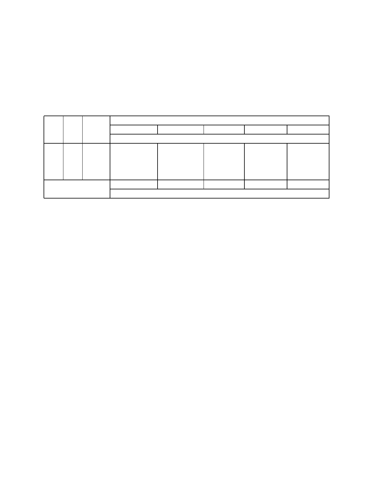
MOTOROLA ASYNCHRONOUS SERIAL COMMUNICATIONS INTERFACE M68HC11
9-8 REFERENCE MANUAL
actual 16 x baud rate will be a binary submultiple (÷1, ÷2, ÷4,... ÷128) of this pres-
caler output as selected by the SCR[2:0] bits. Table 9-1 shows the highest baud rates
that result for various combinations of crystal frequency and prescaler select control
bit values. The actual frequency coming out of this prescaler stage is 16 times the
baud rates listed. Since not all of these entries are of practical use, the ones of interest
have been highlighted in bold. This prescaler is set to its fastest rate by default out of
reset and may be changed at any time. Of course, it makes no sense to change the
baud rate while any SCI transfer is in progress.
RCKB — SCI Baud-Rate Clock Test (Test Modes Only)
This bit is disabled and remains low in any mode other than test or bootstrap modes.
Reset clears this bit. While in test or bootstrap modes, this bit may be written but not
read (reads always return a logic zero). Writing a one to this bit enables a baud-rate
counter test mode where the exclusive-OR of the receiver clock (16 x the baud rate)
and the transmit clock (1 x the baud rate) is driven out the PD1/TxD pin. This control
bit is intended only for factory testing of the MCU.
SCR[2:0] — SCI Baud-Rate Selects
These three bits are used in conjunction with the SCI prescaler bits (see Table 9-1)to
specify the SCI baud rate. The prescale bits, SCP[1:0], determine the highest baud
rate; whereas, the SCR[2:0] bits select an additional binary submultiple (÷1, ÷2, ÷4,
... ÷128) of this highest baud rate. The result of these two dividers working in series
is the 16 x receiver baud-rate clock. Table 9-2 shows the SCI baud rates that result
for various settings of SCR[2:0] and the highest baud rates from Table 9-1. Since not
all of these entries are of practical use, the ones of interest have been highlighted in
bold. The SCR[2:0] bits are not affected by reset and may be changed at any time. Of
course, it makes no sense to change the baud rate while any SCI transfer is in
progress.
Table 9-1 Baud-Rate Prescale Selects
SCP1 SCP0 Division
Factor
Crystal Frequency
223 Hz 8 MHz 4.9152 MHz 4 MHz 3.6864 MH
Highest Baud Rate
0 0 1 131.072K Baud 125.000K Baud 76.80K Baud 62.50K Baud 57.60K Baud
0 1 3 43.691K Baud 41.667K Baud 25.60K Baud 20.833K Baud 19.20K Baud
1 0 4 32.768K Baud 31.250K Baud 19.20K Baud 15.625K Baud 14.40K Baud
1 1 13 10.082K Baud 9600 Baud 5.908K Baud 4800 Baud 4431K Baud
2.1 MHz 2 MHz 1.2288 MHz 1 MHz 921.6 kHz
Bus Frequency (E clock)
M68HC11 ASYNCHRONOUS SERIAL COMMUNICATIONS INTERFACE MOTOROLA
REFERENCE MANUAL 9-9
9.2.3 SCI Control Register 1 (SCCR1)
The SCCR1 contains control bits relate to the 9-bit data character format and the re-
ceiver wake-up feature. Four of the bits in this register are not used and always read
as zeros.
R8 — Receive Data Bit 8
When the SCI system is configured for 9-bit data characters, this bit acts as an extra
(ninth) bit of the RDR. The MSB of received characters is transferred into this bit at the
same time the remaining eight bits are transferred from the serial receive shifter to the
SCDR.
T8 — Transmit Data Bit 8
When the SCI system is configured for 9-bit data characters, this bit acts as the extra
(ninth) bit of the TDR. When the low-order eight bits of a transmit character are trans-
ferred from the SCDR to the serial transmit shift register, this bit is transferred to the
ninth bit position of the shifter. In cases where the sense of this bit is the same as it
was for the previous character, it is not necessary to write to this bit before transmis-
sion of the new character. For example, if the 9-bit format is used to get an extra stop
bit (logic one), the T8 bit is written to one before transmitting the first character, and no
other writes are needed.
M — SCI Character Length
0 = One start bit, eight data bits, one stop bit
1 = One start bit, nine data bits, one stop bit
The M bit controls the character length for both the transmitter and receiver at the
same time. The 9-bit data format is most commonly used for an extra stop bit or in con-
junction with the address-mark wake-up method, but it can also be used for parity.
Table 9-2 Baud-Rate Selects
SCR
2SCR
1SCR
0
Divi-
sion
Factor
Highest Baud Rate (from Table 9-1)
131.072K
Baud 32.768K
Baud 76.80K
Baud 19.20K
Baud 9600
Baud
SCI Baud Rate
0 0 0 1 131.072K Baud 32.768K Baud 76.80K Baud 19.20K Baud 9600 Baud
0 0 1 2 65.536K Baud 16.384K Baud 38.40K Baud 9600 Baud 4800 Baud
0 1 0 4 32.768K Baud 8192 Baud 19.20K Baud 4800 Baud 2400 Baud
0 1 1 8 16.384K Baud 4096 Baud 9600 Baud 2400 Baud 1200 Baud
1 0 0 16 8192 Baud 2048 Baud 4800 Baud 1200 Baud 600 Baud
1 0 1 32 4096 Baud 1024 Baud 2400 Baud 600 Baud 300 Baud
1 1 0 64 2048 Baud 512 Baud 1200 Baud 300 Baud 150 Baud
1 1 1 128 1024 Baud 256 Baud 600 Baud 150 Baud 75 Baud
SCCR1 — SCI Control Register 1 $102C
BIT 7 654321BIT 0
R8 T8 0 M WAKE 0 0 0
RESET: U U 000000

MOTOROLA ASYNCHRONOUS SERIAL COMMUNICATIONS INTERFACE M68HC11
9-10 REFERENCE MANUAL
Mark and space parity are trivial, but odd and even parity require software calcula-
tions.
WAKE — Wake-Up Method Select
0 = Idle line; detection of at least a full character time of idle line causes the receiver
to wake up.
1 = Address mark; a logic one in the MSB position (eighth or ninth data bit depend-
ing on character size selected by M bit) causes the receiver to wake up.
9.2.4 SCI Control Register 2 (SCCR2)
The SCCR2 is the main control register for the SCI subsystem.
TIE — Transmit Interrupt Enable
0 = TDRE interrupts disabled (software polling mode).
1 = An SCI interrupt is requested when TDRE is set to one.
TCIE — Transmit Complete Interrupt Enable
0 = TC interrupts disabled (software polling mode).
1 = An SCI interrupt is requested when TC is set to one.
RIE — Receive Interrupt Enable
0 = RDRF and OR interrupts disabled (software polling mode).
1 = An SCI interrupt is requested when either RDRF or OR is set to one.
ILIE — Idle-Line Interrupt Enable
0 = IDLE interrupts disabled (software polling mode).
1 = An SCI interrupt is requested when IDLE is set to one.
The idle-line function is inhibited while the receiver wake-up function is enabled.
TE — Transmit Enable
0 = SCI transmitter disabled
1 = SCI transmitter enabled
The transmitter does not turn off in the middle of a character. When TE is written to
zero, the transmitter keeps control of the TxD pin until any character in progress (in-
cluding preambles or break characters) is finished. When TE is written from zero to
one, the transmitter sends a preamble character consisting of 10 (11 if M = 1) bits of
logic one. This mechanism can be used to queue an idle character time between the
last character of one message and the first character of the succeeding message. The
procedure would be to wait for TDRE to be set after writing the last character to the
SCDR (this signals that the character has transferred to the shifter to be sent serially).
Then write TE to zero and back to one. Since the last character is still being shifted
out, the transmitter will not relinquish control of the TxD pin, but the act of writing TE
from zero to one causes an idle preamble character to be queued to be sent as soon
SCCR2 — SCI Control Register 2 $102D
BIT 7 654321BIT 0
TIE TCIE RIE ILIE TE RE RWU SBK
RESET: 00000000

M68HC11 ASYNCHRONOUS SERIAL COMMUNICATIONS INTERFACE MOTOROLA
REFERENCE MANUAL 9-11
as the last character from the previous message finishes being shifted out. Finally,
write the first character of the next message to the SCDR. This new character will start
transmitting as soon as the queued idle character finishes.
RE — Receive Enable
0 = SCI receiver disabled
1 = SCI receiver enabled
While the SCI receiver is disabled, the RDRF, IDLE, OR, NF, and FE status flags can-
not become set. If these flags were set, turning off RE does not cause them to be
cleared.
RWU — Receiver Wake Up
0 = Normal SCI receiver operation (wake-up feature not enabled).
1 = Places the SCI receiver in a standby mode where receiver-related interrupts
are inhibited until some hardware condition is met to wake up the sleeping re-
ceiver.
The condition that wakes the receiver up depends on which method of wake up was
specified with the WAKE bit in SCCR1.
Although it is possible for software to write the RWU bit to zero, is very unusual to do
so. The normal sequence is for software to set the RWU bit after deciding that a par-
ticular SCI message is of no interest. Setting the RWU bit causes the receiver to go to
sleep (ignore further receiver interrupt sources) until the start of the next message. Re-
ceiver wake-up logic recognizes when the unimportant message is over and automat-
ically clears the RWU bit to wake up the sleeping receiver.
SBK — Send Break
0 = Normal transmitter operation.
1 = Enable transmitter to send synchronous break characters.
Whenever the SBK bit is written to one, at least one character time of break will be
queued and sent. In the context of the M68HC11, a break character causes the TxD
line to go to logic zero for 10 (11 if M = 1) bit times.
In old teletype systems, a break was caused by simply disconnecting the serial line,
which caused the line to go to logic zero for some asynchronous length of time (usually
as long as the break key was pressed). A receiver seeing a break character produced
by an M68HC11 would receive an all-zero character with a framing error (FE) because
the line would be low where the receiver expected to see a logic-high stop bit.
The break characters in the M68HC11 are synchronous because no partial character
times of the break condition are ever produced. When SBK is set to one, a break char-
acter is queued pending completion of any character currently shifting out of the trans-
mit shift register. When the transmit shift register becomes available, the queued
break character is jammed into the shift register to be serially sent, and, if the SBK bit
is still one, another break is queued. It will always be at least one character time from
when the SBK bit is written back to zero before the transmitter can resume sending
normal characters.
9.2.5 SCI Status Register (SCSR)
The seven status bits associated with the SCI system are located in the SCSR, which
is depicted in the following register. Some of these bits optionally generate hardware

MOTOROLA ASYNCHRONOUS SERIAL COMMUNICATIONS INTERFACE M68HC11
9-12 REFERENCE MANUAL
interrupt requests; whereas, others simply indicate errors in the reception of a charac-
ter. These status bits are automatically set by the corresponding conditions having
been met in the SCI logic. Once set, these bits remain set until software completes a
clearing sequence. The clearing sequences are somewhat automatic in that they are
satisfied by performing functions normally done anyway. For example, to clear the
TDRE flag, software must read the SCSR while TDRE is set, and then write to the
TDR. Since these are exactly the normal steps in response to the TDRE, no instruc-
tions are needed to clear the flag.
TDRE — Transmit Data Register Empty
0 = Not empty; a character was previously written to the SCDR and has not yet
transferred to the transmit shift register to be serially sent.
1 = Indicates a new character may now be written to the SCDR.
In normal transmit operations, this bit is checked before each new character is sent to
see if the SCDR can accept the new data. The SCI transmitter is double buffered so
the TDR holds the second character in line while the transmit serial shift register holds
the character in the process of being transmitted serially. The TDRE flag is cleared by
reading SCSR, followed by a write to the SCDR. TDRE must be read as one during
the read of SCSR, or the first step of the clearing sequence is not satisfied. The TDRE
bit is set to one during reset to indicate that there is no meaningful data in the SCDR.
TC — Transmit Complete
0 = The transmitter is busy sending a character, preamble, or break character.
1 = The transmitter has completed sending and has reached an idle state.
This bit is useful in systems where the SCI is driving a modem. When TC is set at the
end of a transmission, the modem can be disabled. In older ACIA and SCI systems,
the TDRE status bit was the only indication that a transmission was near completion.
Since TDRE only indicated that the last character had transferred to the transmit shift
register, software had to delay an amount of time greater than or equal to the time it
took for this last character to finish transmitting serially. Since the delay time depended
on the baud rate, it was relatively difficult to know when it was safe to disable the mo-
dem. The TC bit on the M68HC11 offers a much more convenient way to tell when the
transmitter has completed sending. The TC flag is cleared by reading SCSR, followed
by a write to the SCDR. TC must be read as one during the read of SCSR, or the first
step of the clearing sequence is not satisfied. The TC bit is set to one during reset to
indicate that the transmitter is not busy transmitting anything.
RDRF — Receive Data Register Full
0 = Not full; nothing has been received since the last character was read out of the
SCDR.
1 = A character has been received and has transferred from the receive shift reg-
ister to the parallel SCDR where software can read it.
SCSR — SCI Status Register $102E
BIT 7 654321BIT 0
TDRE TC RDRF IDLE OR NF FE 0
RESET: 11000000

M68HC11 ASYNCHRONOUS SERIAL COMMUNICATIONS INTERFACE MOTOROLA
REFERENCE MANUAL 9-13
This is the normal indication that a character has been received by the SCI. The NF
and FE status bits provide additional information about this normally received charac-
ter in the SCDR. If set, the OR flag would indicate that another character was serially
received and was ready to be transferred to the SCDR, but the previously received
character was not yet read. Software should check RDRF, OR, NF, and FE to tell if
there was any error in the reception of a character (RDRF should be set and the other
three flags should be clear). The RDRF flag is cleared by reading SCSR, followed by
a read of the SCDR. RDRF must be read as one during the read of SCSR, or the first
step of the clearing sequence is not satisfied. Since the NF and FE flags are set at the
same time as RDRF, the clearing sequence for RDRF will also clear NF and FE if they
were set for this received character.
IDLE — Idle-Line Detect
0 = The RxD line is either active now or has never been active since IDLE was last
cleared.
1 = The RxD line has become idle.
The idle condition is defined as at least a full character time of logic one on the RxD
line. A character time is 10 bit times if M = 0 or 11 bit times ifM=1.TheIDLE flag is
cleared by reading SCSR, followed by a read of the SCDR. IDLE must be read as one
during the read of SCSR, or the first step of the clearing sequence is not satisfied.
Once IDLE has been cleared, it cannot be set again until the RxD line has been active
and then becomes idle again. The idle-line function is inhibited while the receiver
wake-up function is enabled (RWU = 1).
OR — Overrun Error
0 = No overrun error.
1 = Indicates that another character was serially received and was ready to be
transferred to the SCDR, but the previously received character was not yet
read.
Since the SCI receiver is double buffered, there is a full character time between recep-
tion of a character and when it must be read from the SCDR to avoid an OR caused
by a subsequent character. In an OR condition, the character that caused the OR is
lost, but the previously received character in the SCDR is not disturbed. The NF and
FE status bits are associated with the normally received character in the SCDR (never
the character that caused an OR). The OR flag is cleared by reading SCSR, followed
by a read of the SCDR. OR must be read as one during the read of SCSR, or the first
step of the clearing sequence is not satisfied.
NF — Noise Flag
0 = No noise detected during reception of the character in the SCDR.
1 = Data recovery logic detected noise during reception of the character in the
SCDR.
NF does not generate interrupt requests because it is always associated with the set-
ting of RDRF, which does cause interrupts. Even if the noise is detected early in the
reception of the character, NF is not set until RDRF is set at the end of reception of a
character. Perceived noise in any of the data bit times or the start or stop bit times will
cause NF to be set. During data bit times and the stop bit time, noise is indicated if the
three samples taken near the middle of the bit time do not unanimously agree. During

MOTOROLA ASYNCHRONOUS SERIAL COMMUNICATIONS INTERFACE M68HC11
9-14 REFERENCE MANUAL
reception of the start bit, four additional samples are taken during the first half of the
bit time to detect the leading edge of the bit time and to verify that it is a start bit. If all
seven samples taken during the start bit time are not zero, noise is indicated and NF
is set. Many systems ignore the NF because the data recovery logic has already made
a good first-order attempt to correct the problem. In critical applications, the NF could
be used to generate a request for retransmission of the questionable data. The NF flag
is cleared by reading SCSR followed by a read of the SCDR. NF must be read as one
during the read of SCSR, or the first step of the clearing sequence is not satisfied.
FE — Framing Error
0 = No framing error detected.
1 = A framing error was detected for the character in the SCDR.
Asynchronous serial data reception requires the receiver to properly align the charac-
ter reception frame with the incoming serial data. This alignment is achieved by asyn-
chronously searching for the falling edge of the start bit; alignment is verified by looking
for the expected logic high during the last bit time (stop bit) of the character. If a logic
zero is detected where the stop bit was expected, the FE flag is set. The FE indicator
is not a foolproof indication of improper framing. It is possible for the receiver to be mis-
framed without there being any FE indication because the RxD line could by chance
be high when the receiver expected to see the stop bit.
The FE flag is cleared by reading SCSR followed by a read of the SCDR. FE must be
read as one during the read of SCSR, or the first step of the clearing sequence is not
satisfied.
9.2.6 SCI Data Register (SCDR)
The SCDR shown in the following register is actually two separate registers. When
SCDR is read, the read-only RDR is accessed; when SCDR is written, the write-only
TDR is accessed. In discussions of the SCI system, any of the mnemonics SCDR,
TDR, or RDR might be used to refer to this register location.
9.3 SCI Transmitter
The SCI transmitter (see Figure 9-1) uses an internally generated bit-rate clock to se-
rially shift data out of the TxD pin. A normal transmission is initiated by enabling the
transmitter (setting TE to one) and then writing data to be transmitted to the SCDR.
Since the SCI transmitter is double buffered, a new character may be written to the
transmit queue whenever the TDRE status flag is set to one.
The transmit bit-rate clock is free running, and there is normally no way to know where
a bit clock transition will occur relative to the software instructions that write data to the
TDR. Since transfers to the transmit shift register and transmission of data must be
SCDR — SCI Data Register $102F
BIT 7 6 5 4 3 2 1 BIT 0
R7 R6 R5 R4 R3 R2 R1 R0 RDR (READ)
T7 T6 T5 T4 T3 T2 T1 T0 TDR (WRITE)
RESET: U U U U U U U U

M68HC11 ASYNCHRONOUS SERIAL COMMUNICATIONS INTERFACE MOTOROLA
REFERENCE MANUAL 9-15
synchronized to this bit-rate clock, there will be an uncertainty about exactly when a
character will start being transmitted relative to when it was written to the TDR. The
transmit bit-rate clock is free running as opposed to being started when a character is
written to the TDR.
Transmitter logic adds a zero start bit and a one stop bit to the data characters pre-
sented by the CPU for transmission. The transmitter can be configured to send char-
acters with eight (M = 0) or nine (M = 1) data bits. When the TDR is able to accept a
new data character, the TDRE status flag is set, and an interrupt can optionally be gen-
erated. Another status flag (TC) and optional interrupt are produced when the trans-
mitter has finished sending everything in its queue. In addition to data characters, the
transmitter is capable of sending idle-line characters and break characters, which are
useful in multi-drop SCI networks. The transmitter is double buffered, which means
that one character can be in the parallel TDR while another is in the transmit shift reg-
ister being sent. In the case of queued idle and break characters, three characters can
be in the queue, but no more than two can be data characters. The last topic of dis-
cussion for the transmitter will be the TxD pin buffer. This flexible buffer can be used
to control what happens to the TxD pin when the transmitter is finished using the pin.
9.3.1 Eight- and Nine-Bit Data Modes
The M bit in the SCCR1 determines the length of SCI characters for both the transmit-
ter and receiver. The most common configuration is one start bit, eight data bits, and
one stop bit, which is selected by M equals zero. When M equals one, characters are
composed of one start bit, nine data bits, and one stop bit. In this 9-bit data mode, the
low-order eight bits come from the normal TDR, and the ninth bit comes from the T8
bit of SCCR1. Data is transmitted LSB first, and this ninth bit becomes the new MSB,
which is transmitted just before the stop bit. Since this bit is adjacent to the stop bit, it
can be used as an extra stop bit by setting T8 to one.
Another common use for the 9-bit data format is in conjunction with the address-mark
variation of receiver wake up. In a multi-drop SCI network, all receivers evaluate the
first characters of a message to decide whether or not this message is important to this
receiver. If not, receiver wake up may be activated by writing a one to the RWU bit in
SCCR2. A one in RWU causes the receiver to ignore any other characters in the mes-
sage, thus allowing the MCU to perform more useful functions than responding to in-
terrupts from the SCI. The SCI receiver is still monitoring characters normally except
that status flags and interrupts are not being produced. When address-mark wake up
is being used, the SCI receive logic automatically clears RWU when it sees a character
whose MSB is one. The one in the MSB of a character indicates that this character is
the first addressing character of a new message; thus, all receivers should wake up
and evaluate this character. The 9-bit data format allows for full 8-bit data characters
to be used in the body of a message while the ninth bit acts as the address marker.
The first character of each message will have this ninth bit set to one; whereas, the
remaining characters in the message will have a zero in this ninth bit. Address-mark
wake up can be used with 8-bit data format, but message characters could only use
the lower seven bits for information.
The ninth bit can also be used as a parity bit. Mark or space parity can be produced

MOTOROLA ASYNCHRONOUS SERIAL COMMUNICATIONS INTERFACE M68HC11
9-16 REFERENCE MANUAL
by simply making T8 equals one or T8 equals zero, respectively. Odd and even parity
require software calculations with the resulting parity-bit value stored in T8. A new T8
value will have to be calculated for each serial character.
9.3.2 Interrupts and Status Flags
Two status flags are associated with the SCI transmitter. These flags are read by soft-
ware to tell when the corresponding condition exists. This technique is called polling.
Alternatively, a local interrupt enable bit can be set to enable each of these status con-
ditions to generate interrupt requests when the corresponding condition is present.
This technique is called an interrupt-driven operation. Status flags are automatically
set by hardware logic conditions, but software clears these flags, which provides an
interlock mechanism for logic to know when software has noticed the status indication.
The software clearing sequence for these status flags is automatic in that functions
normally performed in response to the status flags also satisfy the conditions of the
clearing sequence.
When the transmitter is first enabled (TE written to one), the TDRE and TC flags are
normally already set. The SCI transmitter should be initialized in such a manner that
the system can handle these interrupts before the TE bit is written to one because an
immediate interrupt can occur from these sources.
The TDRE flag indicates that there is room in the transmit queue to store another data
character in the TDR. The TIE bit is the local interrupt mask for TDRE. When TIE is
zero, TDRE must be polled; when TIE is one, an interrupt is requested whenever
TDRE is one. To clear TDRE, the user must read SCSR while TDRE is one, then write
to SCDR.
The TC flag indicates that the transmitter has finished transmitting everything in its
queue, including any idle preamble or break character that has been queued. The
TCIE bit is the local interrupt mask for TC. When TCIE is zero, TC must be polled;
when TCIE is one, an interrupt is requested whenever TC is one. To clear TC, the user
must read SCSR while TC is one, then write to SCDR.
One interrupt vector is associated with the SCI system; therefore, the interrupt service
routine must begin by reading the SCSR to determine which interrupt(s) caused the
service routine to be called. Possible interrupt sources include the two transmitter
sources previously discussed and three receiver-related sources.
9.3.3 Send Break
In the M68HC11, break characters are character-length periods where the TxD line
goes to zero. The character length for all characters, including idle and break charac-
ters, is influenced by the M bit in SCCR1. When M equals zero, all characters are 10
bit times long; when M equals one, all characters are 11 bit times long. Break charac-
ters have no start or stop bits. As long as the SBK control bit is one, break characters
will be queued and sent. The TxD line will continuously remain at zero while break
characters are being sent. When SBK is written back to zero, at least one bit time of
logic one will appear on the TxD line as soon as the last break character is finished.
This high bit time assures that a receiver can detect the falling edge at the beginning

M68HC11 ASYNCHRONOUS SERIAL COMMUNICATIONS INTERFACE MOTOROLA
REFERENCE MANUAL 9-17
of the start bit for the next data character.
If the transmitter is busy transmitting a character when SBK is toggled on and back off
by software, exactly one break character will be produced following completion of the
character that was being transmitted. If the transmitter is idle at the time the SBK bit is
toggled on and off, it is not certain whether one or two break characters will be sent.
When SBK is set to one, a break character is queued. When the transmit shift register
becomes available and synchronization requirements are met with respect to the in-
ternal 1 x baud-rate clock, the queued break character is jammed into the shift register
to be serially sent and, if the SBK bit is still one, another break is queued. The transfer
mechanism from the queue to the shifter is internally synchronized to the 1 x baud-rate
clock; however, the relationship of this clock to operating software is not normally
known. The instructions to write one and then write zero to the SBK bit execute very
quickly relative to a normal baud-rate frequency, but there is still a small probability
that the baud-rate clock edge could occur between writing the one and writing the zero
to SBK.
9.3.4 Queued Idle Character
When the SCI transmitter is not sending some character, it is idle and the TxD line
rests at logic one. This idle-line condition can last for essentially any length of time and
should not be confused with idle characters. Idle characters are character-length pe-
riods where the TxD line goes to logic one. The character length for all characters, in-
cluding idle and break characters, is influenced by the M bit in SCCR1. When M equals
zero, all characters are 10 bit times long; when M equals one, all characters are 11 bit
times long. Idle characters have no start or stop bits.
Idle characters are only produced when the transmitter is enabled from a disabled
state (TE changed from zero to one). The first time the transmitter is enabled, this idle
character acts as a preamble. The character-length period of logic one assures that
any receiver connected to this transmitter will be resynchronized so that it can properly
recognize the leading edge of the start bit for the next character.
Software can queue an idle character into a serial data stream by momentarily turning
TE off and then back on again. This queueing function is useful when using the idle-
line variation of receiver wake up. In a multi-drop SCI network, all receivers evaluate
the first characters) of a message to decide whether or not this message is important
to this receiver. If not, receiver wake up is invoked by writing a one to the RWU bit in
SCCR2. A one in RWU causes the receiver to ignore any other characters in the mes-
sage, thus allowing the MCU to perform more useful functions than responding to in-
terrupts from the SCI. The SCI receiver is still monitoring characters normally except
that status flags and interrupts are not being produced. When idle-line wake up is be-
ing used, the SCI receive logic automatically clears RWU (waking up the receiver)
when it sees a full character time of logic one. During a message, there must never be
any gap between characters within a message because even a single bit time of idle
can trigger wake up if the previous character was $FF. The queued idle function allows
exactly one character time of idle to be inserted into the data steam to maintain max-
imum efficiency and data throughput. Before queued idle was available, software had
to avoid writing to the TDR for two or more character times after seeing TDRE go high,

MOTOROLA ASYNCHRONOUS SERIAL COMMUNICATIONS INTERFACE M68HC11
9-18 REFERENCE MANUAL
which caused the TxD line to go idle for enough time to trigger RWU. The new queued
idle function is much cleaner and easier to use.
The procedure for queueing an idle character is as follows. Write the last character to
the TDR and wait for TDRE to become set (indicates the last character has transferred
to the transmit shifter to be transmitted serially). Write zero and then write one to TE.
Since the last character is still being transmitted, the transmitter will not give up control
of the TxD pin, and the character being transmitted is undisturbed. The zero-to-one
transition of TE queues the idle character to be sent as soon as the transmit shifter
becomes available. As soon as TE is written back to one, the first character of the next
message may be written to the TDR. In this unusual case, the transmit queue can be
three characters deep: the last data character of the previous message still transmit-
ting, the queued idle character, and the first character of the next message in the par-
allel TDR.
One subtle aspect of the TxD pin buffer logic can be especially useful with the queued
idle function. In the previous queued idle discussion, it was assumed that the transmit-
ter would not relinquish control of the TxD pin because the last character was still be-
ing transmitted, but what if this character is completed while TE is zero? This
completion could occur if the user is using a fast baud rate and the system is so busy
that there is a delay in responding to the TDRE request. The TxD pin will revert to the
general-purpose I/O function. If this scenario is a possibility, write bit 1 of PORTD and
DDRD to one. This configures the PD1/TxD pin to behave as an output and drive a
one if the transmitter relinquishes control of the pin. Since this pin state is identical to
an idle TxD line, the system would see a slightly longer than expected idle character
time.
Since the queuing of an idle character occurs at the rising edge of the TE bit, exactly
one idle character results from the queueing procedure. There is never any possibility
of a second idle character being produced because of uncertainty about the relation-
ship between the software and the internal baud-rate clock (as there was with queued
break characters).
9.3.5 Disabling the SCI Transmitter
Writing a zero to TE requests that the transmitter stop when it can. The transmitter will
finish any transmission in progress before actually shutting down. Only an MCU reset
can cause the transmitter to stop and shut down immediately.
If TE is written to zero when the transmitter is already idle, the pin will revert to its gen-
eral-purpose I/O function (synchronized to the bit-rate clock). If anything is being trans-
mitted when TE is written to zero, that character is completed before the pin reverts to
general-purpose I/O, but any other characters waiting in the transmit queue are lost.
The TC and TDRE flags are set at the completion of this last character even though
TE has been disabled.
9.3.6 TxD Pin Buffer Logic
Several features of the TxD pin buffer logic are especially important to an SCI user.
When the SCI transmitter is enabled, the data direction control is overridden, and the
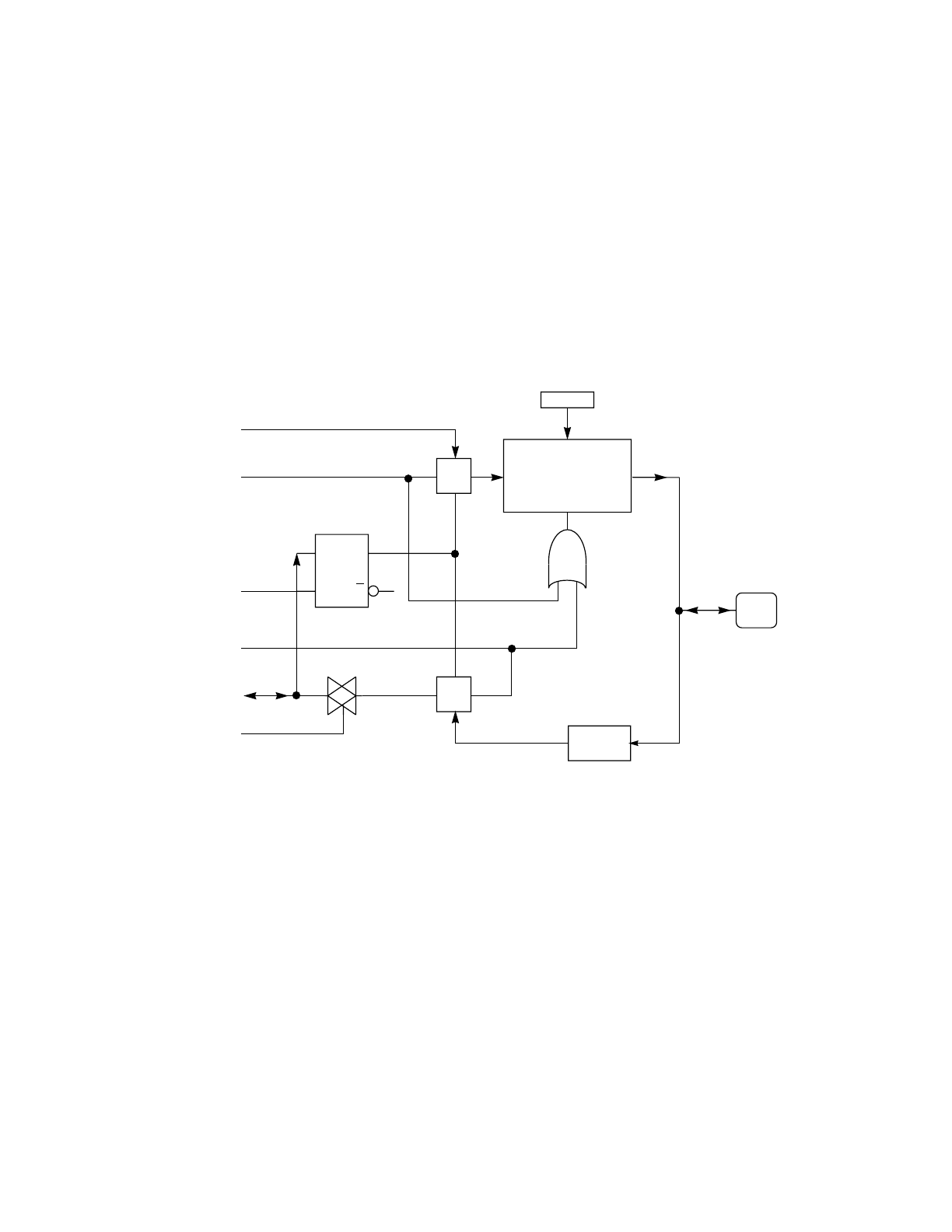
M68HC11 ASYNCHRONOUS SERIAL COMMUNICATIONS INTERFACE MOTOROLA
REFERENCE MANUAL 9-19
output buffer is forced on. When the transmitter is disabled and the transmission in
progress is completed, the pin reverts to being a general-purpose I/O pin controlled by
the PORTD and DDRD registers. In some systems, it is very important to know just
what will happen to the pin when the SCI stops controlling it. Another feature of this
pin buffer allows it to act like an open-collector-type buffer, which helps prevent other-
wise catastrophic problems if two or more drivers connected to this same TxD line
were to become enabled at the same time. Finally, the DDRD1 control bit still influenc-
es what is returned on reads of PORTD even though it is overridden in terms of con-
trolling the output buffer enable.
Figure 9-3 is a simplified block diagram of the TxD pin logic that illustrates the points
of the following discussion. The MOS transistor-level schematic and a more detailed
description of the TxD pin logic are found in 7.3.6 Port D.
Figure 9-3 TxD Pin Logic Block Diagram
Output buffer [1] is enabled by DDRD or by the SCI transmitter on (XMITON) signal.
The XMITON signal is active while the TE bit is one and long enough after TE is written
to zero to allow any currently transmitting character to finish. The DWOM signal deter-
mines whether port D pins will act as open-collector-type drivers or as totem-pole-type
drivers. DWOM simultaneously controls all six port D pins; thus, if open-collector-type
operation is needed on any port D pin(s), it must be used on all six. A fairly common
case might be where the SPI needed open-collector operation so DWOM is set to one.
In this case, the TxD pin needs a pull-up resistor since the internal high-side driver was
disabled.
The data driven out the TxD pin is selected by multiplexer [2]. When the transmitter is
enabled, SCI transmit data will drive the pin buffer. When the transmitter is disabled,
D
C
Q
Q
HFF
OUTPUT
BUFFER
DWOM
PD1
TxD
MUX
A
B
A/B
MUX
A
B
A/B
INPUT
BUFFER
[2]
[4]
[6]
[1]
[3]
XMITON
WPORTD
DDRD1
INTERNAL
DATA BUS
RPORTD
SCI
TRANSMIT
DATA
ENABLE
OPEN DRAIN/TOTEM
[5]

MOTOROLA ASYNCHRONOUS SERIAL COMMUNICATIONS INTERFACE M68HC11
9-20 REFERENCE MANUAL
latched port D data from half flip-flop (HFF) [3] drives the pin buffer. HFF [3] holds the
last data written to PORTD even if the transmitter was enabled at the time.
The DDRD1 control bit provides an enable for pin output buffer [1] and a select to mul-
tiplexer [4]. When PORTD is read, analog switch [5] couples the output of multiplexer
[4] onto the data bus to the CPU. Multiplexer [4] determines what will be returned on
reads of port D. If DDRD1 is one, the output of the port D bit 1 latch [3] is read. If
DDRD1 is zero, pin input buffer [6] is read. When the SCI transmitter is enabled, set-
ting DDRD1 to zero allows software to directly read the current state of the TxD pin as
data is being serially transmitted. In unusual cases, port D bit 1 latch [3] can be used
as a software flag bit that can be written and read without disturbing SCI transmis-
sions.
Probably the most commonly used aspect of the TxD pin logic is the ability to control
what the pin does after the SCI gives up control. For the pin to revert to a driven high,
write DDRD1 and port D bit 1 to ones. For the pin to revert to high impedance, write a
zero to DDRD1. This high-impedance choice is useful in multidrop systems where
more than one transmitter is connected to a common transmit line but no more than
one transmitter is ever simultaneously using the line. The high-impedance choice can
also be used to make a two-wire SCI system where the TxD and RxD pins of the
M68HC11 are tied together and data travels in only one direction at a time (half du-
plex).
Since the M68HC11 is a CMOS device, it is a good idea to select the wired-OR option
with DWOM whenever more than one output driver could potentially try to drive the
same line.
9.4 SCI Receiver
The SCI receiver is responsible for synchronization to the serial data stream and re-
covery of data characters. Since the data stream has no clock, data recovery depends
on the transmitting device and the receiving device operating at close to the same
baud rate. The SCI system can tolerate a moderate amount of system noise without
losing any information.
The SCI receive function is somewhat more difficult than the transmit function due to
the asynchronous nature of incoming serial data. A significant amount of discussion
will be devoted to the way the M68HC11 recognizes a start bit because this procedure
determines the amount of baud-rate frequency mismatch that can be tolerated and
gives an indication of how well this SCI receiver can handle noise. Second, basic dou-
ble-buffered receive functions are discussed. Finally, the two variations of the receiver
wake-up function are explained.
9.4.1 Data Sampling Technique
The receiver front-end logic uses a sampling clock that is 16 times the baud-rate fre-
quency. This sampling clock is called the RT clock in the following discussion, and one
RT is understood to be one-sixteenth of a bit time. In the following figures, the RT clock
cycles are numbered from one (start of a bit time) to 16 (end of a bit time).

M68HC11 ASYNCHRONOUS SERIAL COMMUNICATIONS INTERFACE MOTOROLA
REFERENCE MANUAL 9-21
When the receiver is first enabled and after the reception of a stop bit at the end of a
frame, an asynchronous search is initiated to find the leading edge of the next start bit.
The goal of this asynchronous search is to gain bit-time synchronization between the
serial data stream and the internal RT clock. Once synchronization has been estab-
lished, the RT clock controls where the MCU perceives the bit-time boundaries to be.
The first step in locating a start bit is to find a sample where RxD is zero preceded by
three consecutive samples of logic one. These four samples are called start-bit quali-
fiers. Until the start-bit qualifiers are detected, the RT clock is reset to state RT1 after
each sample. Once the qualifiers are found, the beginning of a start bit is tentatively
assumed, and subsequent samples are assigned successive RT state numbers. Next,
start-bit verification samples are taken at RT3, RT5, and RT7. If any two of the three
verification samples are logic ones, the low at RT1 is assumed to have been noise,
and the asynchronous search is started again. When the start-bit qualifiers and the
start-bit verification requirements are met, synchronization has been achieved, and
the RT count state is used to determine the position of bit-time boundaries.
During each bit time, including the start and stop, data samples are taken at RT8, RT9,
and RT10 to determine the logic sense of the bit time and to (possibly) set a working
NF. The logic sense of the bit time is considered to be the majority of all samples taken
during the bit time. If any sample disagrees with the rest, the working NF is set. Even
if the samples at RT8, RT9, and RT10 suggest it should be one, the start bit time is
always assumed to be zero. The primary reason for this assumption is to avoid an ac-
cidental wake up while using the idle-line variation of receiver wake up. If the previous
character had been all ones ($FF), the stop bit and the erroneous logic high in the new
start bit would combine to make a full character time of logic one and would errone-
ously wake up the receiver. Also, at least three of the four samples at RT1, RT3, RT5,
and RT7 were logic zero, which would contradict a decision of logic one based on the
samples at RT8, RT9, and RT10.
If there is any disagreement among the samples taken during any bit time in a frame
(including the start and stop), the working NF is set. At the end of a character recep-
tion, data is transferred from the receive shifter to the parallel RDR, and the RDRF flag
is set. If noise was detected during reception of the character, the NF is set at the same
time as RDRF.
Figure 9-4 shows the details of the ideal case of start-bit recognition. All samples tak-
en at [1] detect logic ones on the RxD line and correspond to the idle-line time or a
stop-bit time prior to this start bit. At [2] a logic-zero sample is preceded by three logic-
one samples. These four samples are called the start-bit qualifiers. The beginning of
the start bit time is tentatively perceived to occur between the third logic-one sample
and the logic-zero sample of the start qualifiers. Next, the samples at RT3, RT5, and
RT7 [3] are taken to verify that this bit time is indeed the start bit. The samples at RT8,
RT9, and RT10 are called the data samples [4]. In any bit time other than the start bit,
these samples would drive a majority voting circuit to determine the logic sense of the
bit time. In the special case of the start bit time, the bit value is forced to be zero inde-
pendent of what the data samples at RT8, RT9, and RT10 suggest.
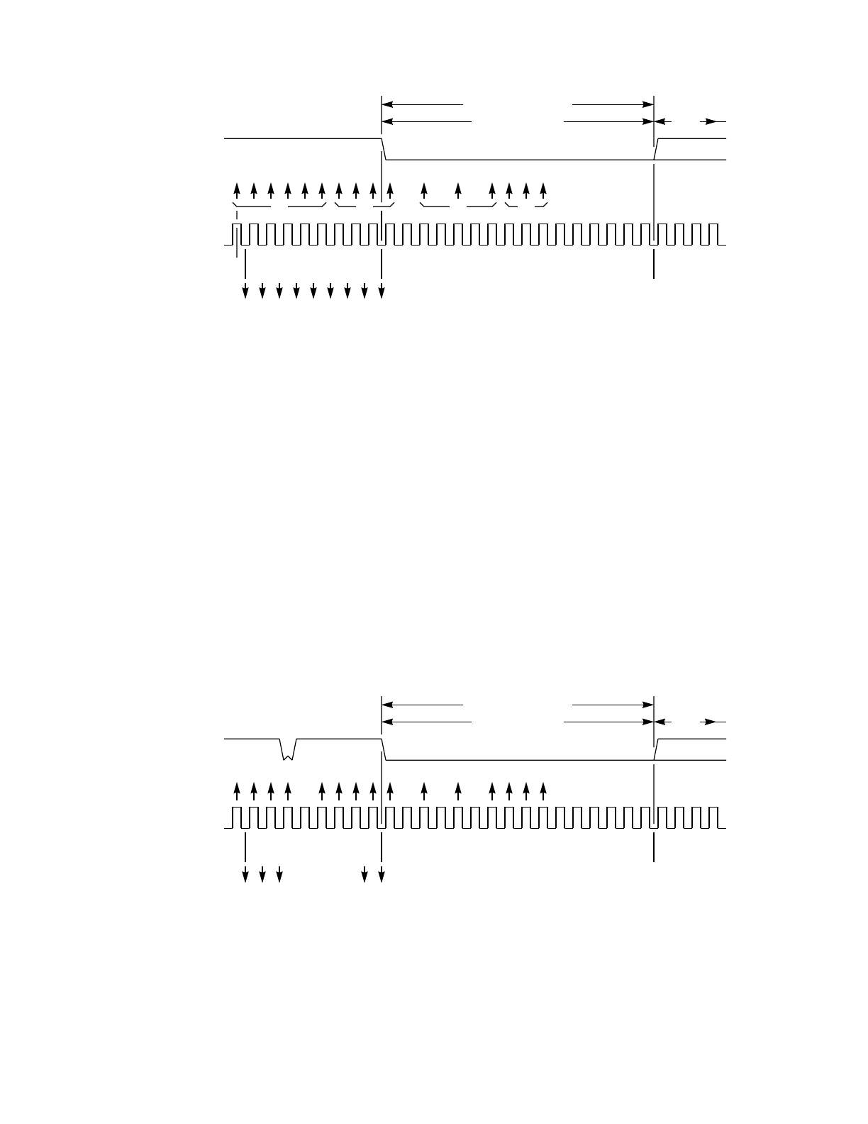
MOTOROLA ASYNCHRONOUS SERIAL COMMUNICATIONS INTERFACE M68HC11
9-22 REFERENCE MANUAL
Figure 9-4 Start Bit — Ideal Case
In this ideal case, the actual start bit and the perceived start bit match. The resolution
of the RT clock leads to an uncertainty about the exact placement of the leading edge
of the start bit. The uncertainty in the placement of the edge will be one-sixteenth of a
bit time.
Figure 9-5 shows what occurs if noise causes a sample to be erroneously detected
as a zero before the actual beginning of the start bit. Logic-zero sample [1] in conjunc-
tion with the three preceding samples of logic one meet the conditions for start quali-
fication; thus, logic tentatively perceives the start bit as beginning here. Subsequent
start-verification samples at RT3 and RT5 [2] are both ones; therefore, the tentative
placement of the start edge is rejected, and the search is restarted. When the sample
at the actual beginning of the start bit is detected, the preceding three samples are
ones; the start bit is now perceived to begin here. In this case, the three samples taken
at RT3, RT5, and RT7 now verify that the start bit has been found.
Figure 9-5 Start Bit — Noise Case One
Figure 9-6 is similar to the previous case except noise [1] is now closer to the actual
beginning of the start bit. The noise sample and the preceding three ones meet the
RT1
RT1
RT1
RT1
RT1
RT1
RT1
RT1
RT1
RT1
RT1
RT2
RT3
RT4
RT5
RT6
RT7
RT8
RT9
RT10
RT11
RT12
RT13
RT14
RT15
RT16
RT2
RT3
[1] [2] [3] [4]
0101011 011 010101
ACTUAL START BIT
PERCEIVED START BIT
LSB
RT4
RxD PIN
SAMPLES
RT CLOCK
(16X BAUD RATE)
RT CLOCK
STATE
RESET RT
RT1
RT1
RT1
RT1
RT1
RT2
RT3
RT4
RT5
RT1
RT1
RT2
RT3
RT4
RT5
RT6
RT7
RT8
RT9
RT10
RT11
RT12
RT13
RT14
RT15
RT16
RT2
RT3
0101010 01010101
ACTUAL START BIT
PERCEIVED START BIT
LSB
RT4
RxD PIN
SAMPLES
RT CLOCK
(16X BAUD RATE)
RT CLOCK
STATE
RESET RT [2]
[1]
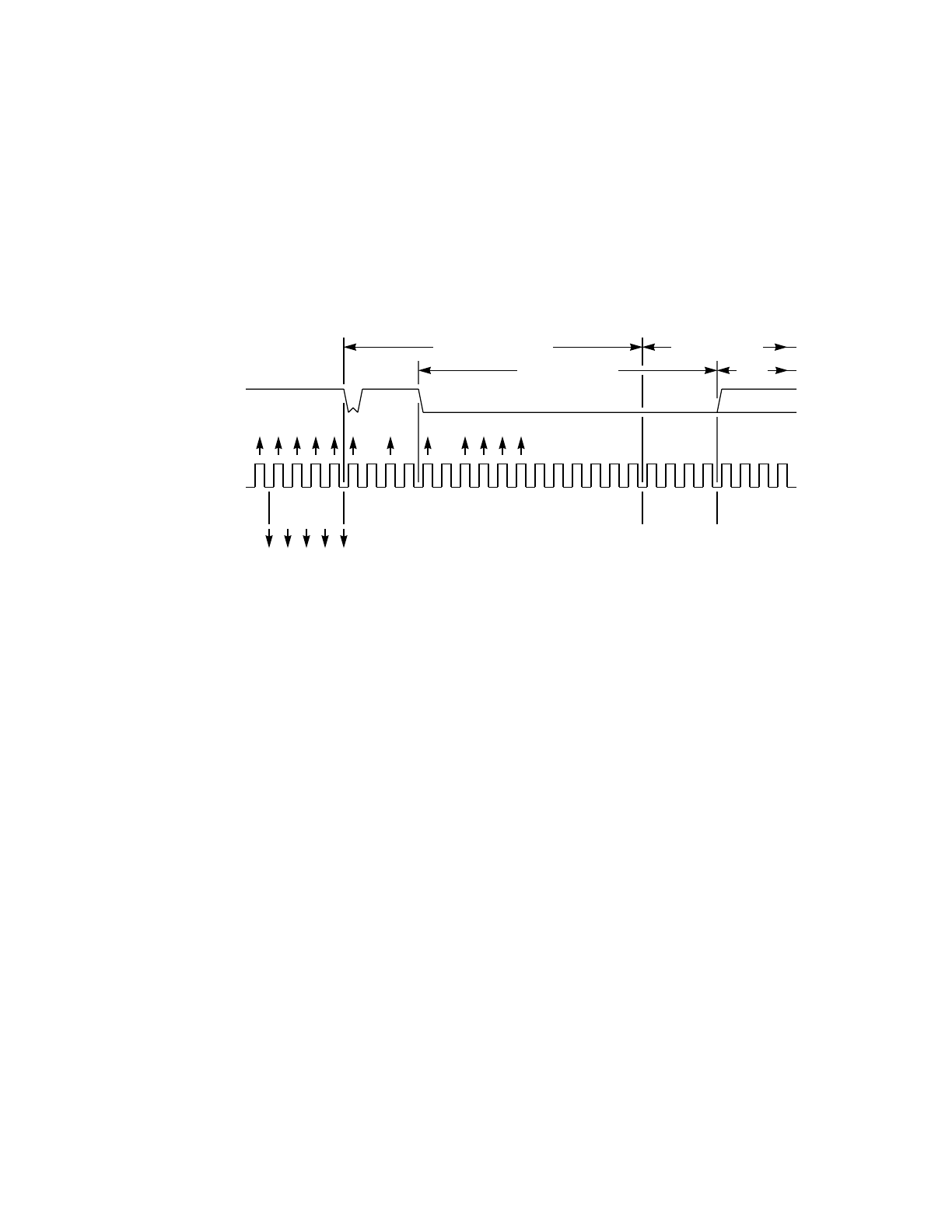
M68HC11 ASYNCHRONOUS SERIAL COMMUNICATIONS INTERFACE MOTOROLA
REFERENCE MANUAL 9-23
start qualification requirements. The start-verification sample at RT3 [2] is one, which
will cause the working NF to be set. The samples at RT5 and RT7 [3] are zeros. Since
two out of three of the start-verification samples are correct, the original perceived po-
sition for the beginning of the start bit is accepted. The RT clock will roll over from state
16 to state 1 [4], and bit-time misalignment [5] will continue for the remainder of this
character. (A one-to-zero transition in the data character would cause the alignment
to be readjusted.) Even though the perceived alignment of the serial data to the RT
clock is technically incorrect, the data samples at RT8, RT9, and RT10 fall well within
the actual bit time. This character would almost certainly be received correctly; how-
ever, the NF will be set to inform the user of the questionable character.
Figure 9-6 Start Bit — Noise Case Two
Figure 9-7 shows a burst of noise [1] causing two samples to detect erroneous zeros.
The sample at RT5 would cause the working NF to set. Even though this example
shows a worst-case alignment of perceived bit-time boundaries to actual bit-time
boundaries, the data samples taken at RT8, RT9, and RT10 will fall within the actual
bit time, and data recovery should still be successful. Perceived bit-time boundary [2]
is almost half a bit time too soon; however, the data samples for LSB [3] still fall within
the actual LSB bit time. This example is a theoretical case, and such gross noise
should never be seen in an actual application. This case is an indication of how toler-
ant the SCI receiver is to system noise.
RT1
RT1
RT1
RT1
RT1
RT1
RT1
RT2
RT3
RT5
RT6
RT7
RT8
RT4
RT5
RT6
RT7
RT8
RT9
RT10
RT11
RT12
RT13
RT14
RT15
RT16
RT2
RT3
0101010 011 01
ACTUAL START BIT
PERCEIVED START BIT
LSB
RT4
RxD PIN
SAMPLES
RT CLOCK
(16X BAUD RATE)
RT CLOCK
STATE
RESET RT
[2]
[1]
[3]
[4]
PERCEIVED LSB
[5]
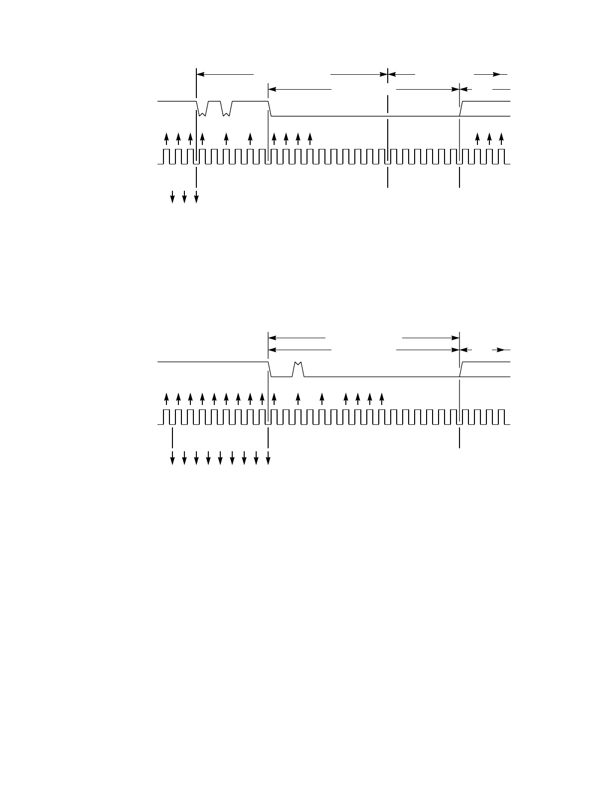
MOTOROLA ASYNCHRONOUS SERIAL COMMUNICATIONS INTERFACE M68HC11
9-24 REFERENCE MANUAL
Figure 9-7 Start Bit — Noise Case Three
Figure 9-8 depicts the case of noise causing an erroneous sample of one early in the
start bit. In this case, the NF would be set due to the one at sample RT3. The alignment
of the perceived bit-time boundary matches that of the actual bit-time boundary.
Figure 9-8 Start Bit — Noise Case Four
Figure 9-9 shows a gross burst of noise [1] during the start-verification samples. The
two logic-one samples at RT5 and RT7 cause the one-to-zero transition at the actual
beginning of the start bit to be rejected as the perceived start bit. Since there are no
more cases of three logic-one samples in a row [2], the start bit is never detected. Be-
cause the circuit could not locate the start bit, the frame will be received as a framing
error, be improperly received, or be missed entirely, depending on the data in the
frame and when the start search logic synchronized on what it thought was a start bit.
This example shows two independent noise incidents that are specifically positioned
within a frame. Of the six cases of noise during the start-bit search, this case is the
only one that causes incorrect data reception.
RT1
RT1
RT1
RT1
RT1
RT2
RT3
RT5
RT6
RT7
RT8
RT4
RT5
RT6
RT7
RT8
RT9
RT10
RT11
RT12
RT13
RT14
RT15
RT16
RT2
RT3
0101010010
ACTUAL START BIT
PERCEIVED START BIT
LSB
RT4
RxD PIN
SAMPLES
RT CLOCK
(16X BAUD RATE)
RT CLOCK
STATE
RESET RT
[1]
PERCEIVED LSB
RT9
RT10
[2]
[3]
000
RT1
RT1
RT1
RT1
RT1
RT1
RT1
RT2
RT3
RT4
RT5
RT6
RT7
RT8
RT9
RT10
RT11
RT12
RT13
RT14
RT15
RT16
RT2
RT3
01011101010101
ACTUAL START BIT
PERCEIVED START BIT
LSB
RT4
RxD PIN
SAMPLES
RT CLOCK
(16X BAUD RATE)
RT CLOCK
STATE
RESET RT
11
RT1
RT1
RT1
RT1
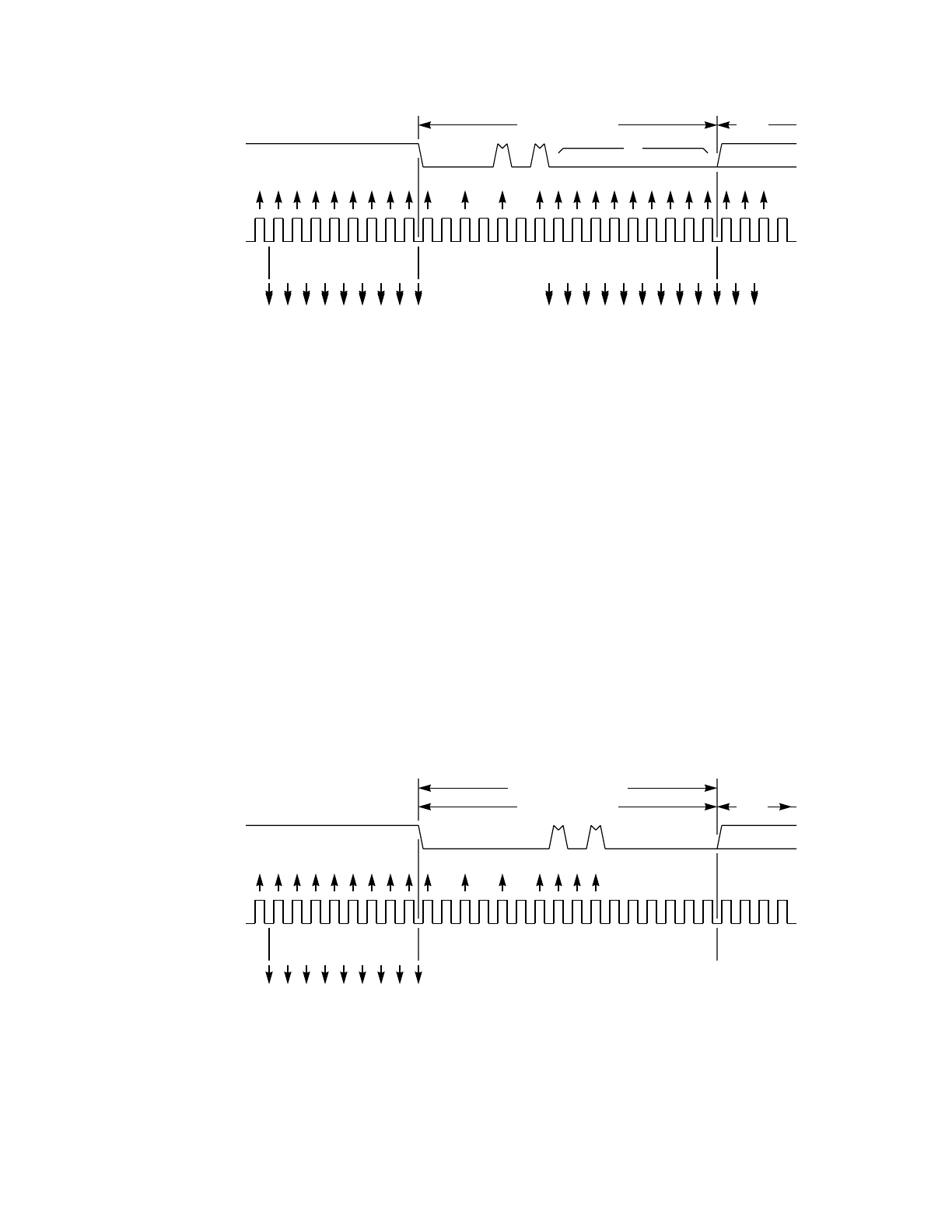
M68HC11 ASYNCHRONOUS SERIAL COMMUNICATIONS INTERFACE MOTOROLA
REFERENCE MANUAL 9-25
Figure 9-9 Start Bit — Noise Case Five
The final start-bit case shown in Figure 9-10 shows a burst of noise in the middle of
the start bit time. The noise [1] causes two out of three data samples to be erroneously
detected as ones. The start-bit logic forces this bit to be detected as a zero even
though the majority of samples RT8, RT9, and RT10 suggest it should be one. The
majority of all seven samples taken during the start bit time agree with the forced zero.
Another advanced feature of the data sampling technique allows the RT clock to be
resynchronized on any valid one-to-zero transition in a frame. Data is constantly being
sampled and shifted into a 16 x baud-rate shift register. A one-to-zero transition is in-
dicated by the pattern (1110d0d0d0), which corresponds to three logic-one samples
preceding the falling edge and logic-zero samples at RT1, RT3, RT5, and RT7. (As
long as no more than one of the samples at RT3, RT5, and RT7 was a one, the falling
edge would be recognized.) This feature does not help a worst-case analysis. Howev-
er, this feature improves the probability of proper alignment between perceived bit
times and actual bit times in the data stream, thus improving the reliability of normal
data reception.
Figure 9-10 Start Bit — Noise Case Six
After a framing error is detected (provided a break was not detected at the same time),
RT1
RT1
RT1
RT1
RT1
RT1
RT1
RT2
RT3
RT4
RT5
RT6
RT7
010101111 0101
ACTUAL START BIT
NO START BIT FOUND—SEE TEXT
LSB
RxD PIN
SAMPLES
RT CLOCK
(16X BAUD RATE)
RT CLOCK
STATE
RESET RT
11
RT1
RT1
RT1
RT1
[2]
[1] 1 000000ddd
RT1
RT1
RT1
RT1
RT1
RT1
RT1
RT1
RT1
RT1
RT1
RT1
RT1
RT1
RT1
RT1
RT1
RT1
RT2
RT3
RT4
RT5
RT6
RT7
RT8
RT9
RT10
RT11
RT12
RT13
RT14
RT15
RT16
RT2
RT3
01111101010101
ACTUAL START BIT
PERCEIVED START BIT
LSB
RT4
RxD PIN
SAMPLES
RT CLOCK
(16X BAUD RATE)
RT CLOCK
STATE
RESET RT
11
RT1
RT1
RT1
RT1
[1]

MOTOROLA ASYNCHRONOUS SERIAL COMMUNICATIONS INTERFACE M68HC11
9-26 REFERENCE MANUAL
the three logic-one samples leading to start-bit qualification are forced into the high-
speed shift register. This procedure is analogous to pretending the stop bit of the mis-
framed character was really a logic one. The forced logic-one samples are positioned
at RT14, RT15, and RT16 of the perceived stop bit in an attempt to permit normal re-
ception to proceed. If the samples were not forced to ones, the subsequent start bit
could be missed. A break is detected when a framing error occurs and the data char-
acter associated with it is all zeros. In the case of a break detect, the artificial start edge
is not forced.
From an understanding of how character alignment is achieved and where the logic
sense of a bit time is sampled, it is possible to calculate the worst-case baud-rate mis-
match that can be tolerated between two SCI devices. In this worst-case analysis, no
one-to-zero transitions are assumed to occur within the character to cause realign-
ment. The noise cases discussed previously are ignored because they do not apply to
normal reception. In the case of baud-rate mismatch, the data sampling technique
may be unable to recover correct data in the presence of gross noise.
9.4.2 Worst-Case Baud-Rate Mismatch
Two cases must be considered and each of these cases must be modified for normal
8-bit data format and optional 9-bit data format. In the first case, a too-slow transmitting
device sends characters to this SCI receiver. In the second case, a too-fast transmit-
ting device is operating above the ideal baud rate. When the accumulated bit-time
alignment error causes more than one of the three data samples for the stop bit time
to fall outside the actual stop bit time, an error has occurred. In both cases, assume
the receiver is operating at the ideal baud rate for reference, which should provide the
basis for any worst-case baud-rate analysis. For most users, the amount of mismatch
that can be tolerated is much more than the amount that is ever likely to be encoun-
tered.
Figure 9-11(a) shows a worst-case slow signal on RxD relative to the RT clock states
of the 16 x receiver RT clock. The alignment of the falling edge of start bit [1] in Figure
9-11(a) and [3] in Figure 9-11(b) shows the uncertainty resulting from the resolution
of the RT clock. Only two out of the three data samples for the stop bit fall within actual
stop bit [2]. Majority sampling can still correctly detect the stop-bit value of one, even
if the MSB had been a zero. Of course, this worst-case analysis is not considering oth-
er errors or noise.
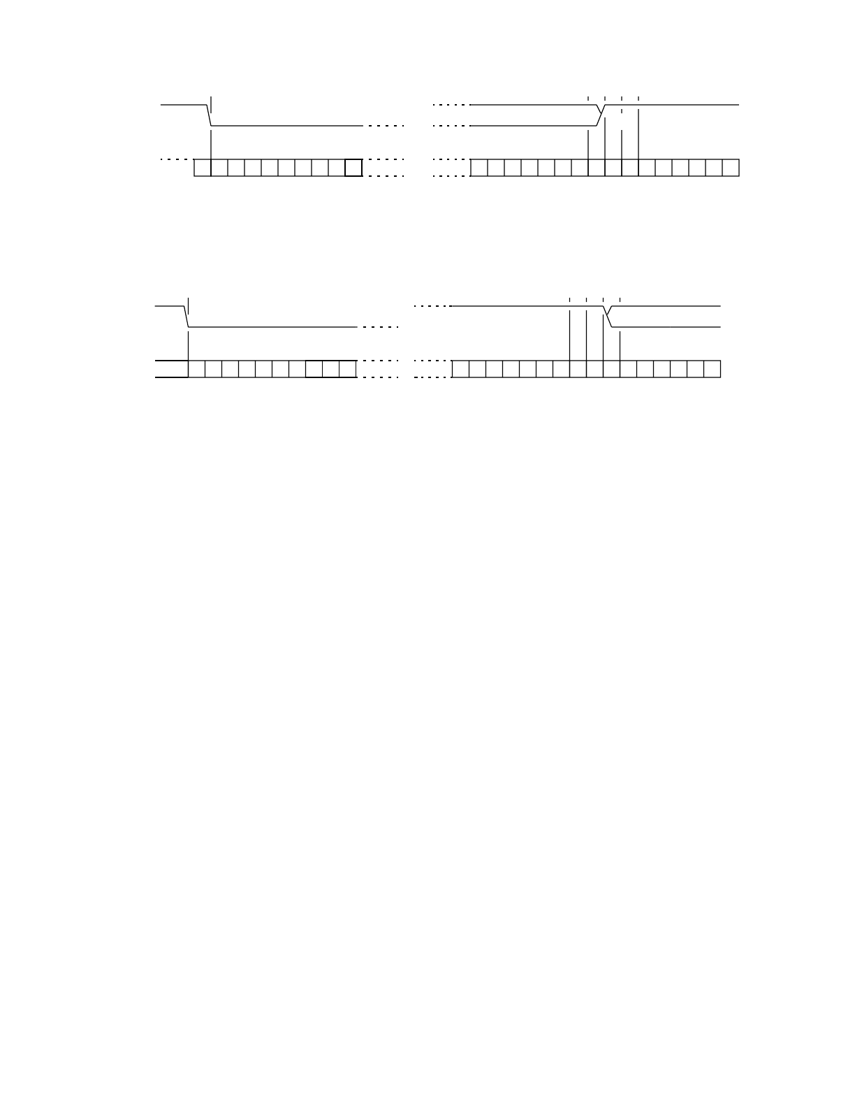
M68HC11 ASYNCHRONOUS SERIAL COMMUNICATIONS INTERFACE MOTOROLA
REFERENCE MANUAL 9-27
(a) Receive Data Slower Than Receiver Baud Rate
(b) Receive Data Faster Than Receiver Baud Rate
Figure 9-11 Baud-Rate Frequency Tolerance
For 8-bit data format, the ratio of the frequency of incoming data to the frequency of
the receiver baud-rate clock can be written as follows:
(9 bit times) ÷ [15/16 + 8(16/16) + 8/16]
The nine bit times are measured from the leading edge of the start bit to the trailing
edge of the MSB (the stop bit was not measured although it could have been if a dif-
ferent denominator time had been used). The 15/16 is the amount of overlap between
the actual start bit and the perceived start bit. For convenience, multiply everything by
16 to obtain measurements in terms of RT clock cycles as opposed to baud-rate clock
cycles. The 8(16/16) corresponds to the eight bit times of data between the perceived
start and stop bits. The 8/16 corresponds to the portion of the perceived stop bit time
to the boundary between the actual MSB and stop bit. This ratio calculates as follows:
(9 x 16)/(15 + 8 x 16 + 8) = 144/(15 + 128 + 8) = 144/151 = 95.36%
The equivalent calculation for 9-bit data format would be
(10 x 16)/(15 + 9 x 16 + 8) = 160/(15 + 144 + 8) = 160/167 = 95.81%
Figure 9-11(b) can be used in a similar way to derive the calculations for the fastest
serial data rate that can be tolerated. The actual start bit and the perceived start bit
both begin at [3]. In this case, measure the time for the complete actual frame, which
ends between RT clock states 9 and 10 of the perceived stop bit. The calculation for
8-bit data format is
PERCEIVED START BIT
RxD PIN
1234567891011121314151612345678910
RECEIVER
RT CLOCK
STATE
[2] STOPMSBSTART
PERCEIVED STOP BIT
[1]
PERCEIVED START BIT
RxD PIN
1234567891011121314151612345678910
RECEIVER
RT CLOCK
STATE
[4]
STOP IDLE OR NEXT CHARACTER
START
PERCEIVED STOP BIT
[3]

MOTOROLA ASYNCHRONOUS SERIAL COMMUNICATIONS INTERFACE M68HC11
9-28 REFERENCE MANUAL
(10 x 16)/(9 x 16 + 9) = 160/153 = 104.56%
The equivalent calculation for 9-bit data format is
(11 x 16)/(10 x 16 + 9) = 176/169 = 104.14%
For 8-bit data format, the baud-rate variation that can be tolerated is about ±4.5%; for
9-bit data format, the variation is about ±4%. This analysis assumes one of the devices
was operating at the exact baud-rate frequency, and the calculations show how much
the other device could vary from this. One device operating four percent too slow can-
not communicate with another device operating four percent too fast.
9.4.3 Double-Buffered Operation
The SCI receiver in the M68HC11 is double buffered, which means that the receiver
can have up to two characters in it at any given moment. One of the characters is in a
readable parallel receive data buffer (SCDR); another could be shifting into the receive
serial shift register. This double-buffered arrangement gives software some time to no-
tice a received character and read it before the next serial character is finished. With-
out double buffering, the transmitting device would be required to insert delays
between transmitted characters to avoid a receiver overrun. An overrun occurs in a
double-buffered M68HC11 if a serial character is received and is ready to transfer into
the parallel RDR while there is still a previously received character in the RDR. The
transfer could not occur without destroying the previously received character.
9.4.4 Receive Status Flags and Interrupts
Five status flags are associated with the SCI receiver. RDRF is set and optionally gen-
erates an interrupt request when a character has been received and transferred into
the parallel RDR. The OR flag is set and optionally generates an interrupt request in-
stead of RDRF (if RDRF was already set when a new character was ready to be trans-
ferred into the parallel RDR). When an overrun takes place, the new character is lost,
and the character that was in its way in the parallel RDR is undisturbed. The NF and
FE flags provide additional information about the character in the parallel RDR. Since
NF and FE are always accompanied by RDRF and since RDRF already generates an
interrupt request, NF and FE do not. The last receiver status flag and interrupt source
comes from the IDLE flag. The RxD line is idle if it has constantly been at logic one for
a full character time. The IDLE flag is set only after the RxD line has been busy and
becomes idle, which prevents repeated interrupts for the whole time RxD remains
idle.
Status flags are set by the SCI logic in response to specific conditions in the receiver.
These flags can be read (polled) at any time by software. Three of the flags (RDRF,
OR, and IDLE) can also optionally generate an automatic interrupt request. The RIE
is a local enable for both RDRF and OR. If RIE is set to one, RDRF and OR generate
interrupts whenever either is set to one. If RIE is zero, RDRF and OR do not generate
interrupts, and the receiver operates in polled mode. ILIE works similarly as a local en-
able for the IDLE status flag. When ILIE is set to one, an interrupt request is generated
whenever IDLE is a one. When ILIE is zero, the IDLE status flag does not generate
interrupt requests. When the receiver wake-up function is enabled (RWU = 1), setting

M68HC11 ASYNCHRONOUS SERIAL COMMUNICATIONS INTERFACE MOTOROLA
REFERENCE MANUAL 9-29
the IDLE flag is inhibited.
9.4.5 Receiver Wake-Up Operation
The M68HC11 receiver logic hardware also supports a receiver wake-up function,
which is intended for systems having more than one receiver. With this function, a
transmitting device directs messages to an individual receiver or group of receivers by
passing addressing information as the initial byte(s) of each message. Receivers not
addressed activate the receiver wake-up function, which makes these receivers dor-
mant for the remainder of the unwanted message and eliminates any further software
overhead to service the remaining characters of the unwanted message.
The receiver is placed in wake-up mode by writing a one to the RWU bit in the SCCR2
register. While RWU is one, all of the receiver-related status flags (RDRF, IDLE, OR,
NF, and FE) are inhibited (cannot become set). Although RWU can be cleared by a
software write to SCCR2, to do so would be unusual. Normally, RWU is set by soft-
ware and is cleared automatically with hardware by one of the two following methods.
9.4.5.1 Idle-Line Wake Up
To use this receiver wake-up method in an actual system, a software addressing
scheme is established to allow the transmitting device(s) to direct messages to indi-
vidual receivers or groups of receivers. This addressing scheme is purely a software
device and may take any form as long as all transmitting and receiving devices are
programmed to understand the same scheme. The addressing information is usually
the first frame(s) in a message; therefore, uninterested receivers are burdened only
with these minimum addressing frames. All receivers are awake (RWU = 0) when each
message begins. As soon as a receiver determines that the message is not intended
for it, software sets the RWU bit (RWU = 1), which inhibits further flag setting until the
RxD line goes idle at the end of the message. As soon as an idle line is detected by
receiver logic, hardware automatically clears the RWU bit so that the first frame of the
next message can be received. This method of receiver wake up requires a minimum
of one idle-line frame time between messages and no idle time between frames in a
message.
9.4.5.2 Address-Mark Wake Up
In this method of receiver wake up, all serial characters consist of seven (eight if M =
1) information bits and an MSB, which is used to indicate an address character (when
set to one (mark)). The first character of each message is an addressing character
(MSB is one). All receivers in the system evaluate this character to determine if the
remainder of the message is directed toward this particular receiver. As soon as a re-
ceiver determines that a message is not intended for it, the receiver activates the RWU
function by setting (with a software write) the RWU bit. Since setting RWU inhibits re-
ceiver-related flags, there is no further software overhead for the rest of this message.
When the next message begins, its first character will have its MSB set, which auto-
matically clears the RWU bit and enables normal character reception. The first char-
acter whose MSB is set will also be the first character to be received after wake up
because RWU gets cleared before the stop bit for that frame is serially received. This

MOTOROLA ASYNCHRONOUS SERIAL COMMUNICATIONS INTERFACE M68HC11
9-30 REFERENCE MANUAL
method of wake up allows messages to include gaps of idle time, unlike the earlier idle-
line method, but there is an efficiency loss due to the extra bit time per character (ad-
dress bit) required in all characters.
9.5 Baud-Rate Generator
This discussion, which provides a more detailed description of the baud-rate genera-
tor, is useful to those users who have an odd crystal frequency or some other unusual
requirement. The usual approach to selecting a baud rate is to start from a particular
crystal frequency and select one of the 32 available division factors to arrive at a de-
sired baud rate. If a system uses equipment from other manufacturers (such as a CRT
terminal or host computer), a standard baud rate, such as 9600 baud, is used. Many
applications include SCI networks that do not have to communicate with ordinary
RS232-type sources. In these cases, any frequency can be used as long as all of the
devices in the network use the same baud rate — for example, in the automotive in-
dustry, 32.768K baud has commonly been used. These systems include separate
controllers for various parts of the car and test equipment interfaces. All of the custom
equipment is controlled by the automobile manufacturer. In this environment, high
throughput on the SCI and maximum bus frequency are more important than a cus-
tomary baud rate.
9.5.1 Timing Chain Block Diagram
Figure 9-12 is a block diagram of the SCI baud-rate timing chain. The crystal frequen-
cy is divided by four to get the bus rate PH2 clock. PH2 is the same frequency as E
(but leads E by 90°). The prescale select bits, SCP[1:0], select an initial division factor
of 1, 3, 4, or 13 that drives a series of divide-by-two stages. The rate select bits
(SCR[2:0]) determine where the RT clock will be tapped off of this divider chain. The
RT clock is 16 times the baud-rate frequency. This 16 x baud-rate clock is finally divid-
ed by 16 to get the transmitter baud-rate clock. The actual baud-rate generator func-
tions like this block diagram although the implementation is slightly different to
overcome potential circuit-delay problems. (It is important to the overall SCI circuit de-
sign to maintain minimum delays from PH2 to baud rate clock edges.)
9.5.2 Baud Rates vs. Crystal Frequency
Table 9-3 is a complete listing of all possible baud rates that can be achieved for five
crystal frequencies. The entries most likely to be of interest are in bold.
9.6 SCI Timing Details
The timing information presented in the following paragraphs is much more detailed
than most users need but will help normal users better understand the SCI system.
For rare applications needing this much detail, this discussion is an authoritative ref-
erence source although it is not intended to replace guaranteed data-sheet timing in-
formation.
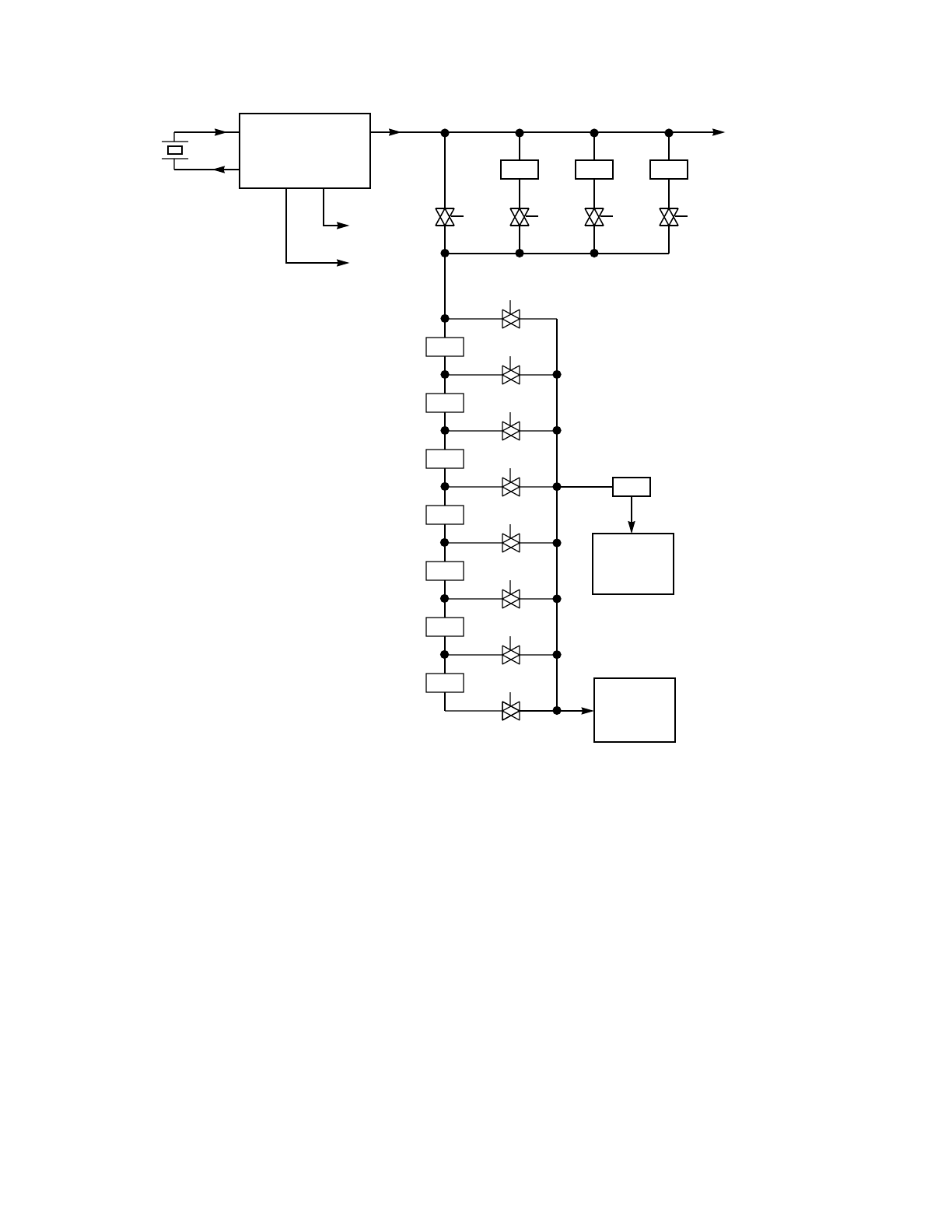
M68HC11 ASYNCHRONOUS SERIAL COMMUNICATIONS INTERFACE MOTOROLA
REFERENCE MANUAL 9-31
Figure 9-12 Baud-Rate Generator Block Diagram
9.6.1 Operation As Transmitter Is Enabled
When the transmitter is initially enabled (writing one to TE), the SCI logic overrides
DDRD control of the PD1/TxD pin, and an initial preamble character is sent. This pre-
amble character is 10 (11 ifM=1)bittimes of continuous logic high at the pin. An un-
certainty arises because all transmissions are synchronized to the relatively slow
baud-rate clock, and the relationship of this clock to running software is normally not
known. Figure 9-13 summarizes the timing details related to transmitter enable.
÷3÷4÷13
OSCILLATOR
AND
CLOCK GENERATOR
(÷4)
XTAL
EXTAL
E
AS
INTERNAL BUS CLOCK (PH2)
1:1
SCP[1:0]
1:00:10:0
÷2
0:0:0
÷2
0:0:1
÷2
0:1:0
÷2
0:1:1
÷2
1:0:0
÷2
1:0:1
÷2
1:1:0
1:1:1
÷16
SCI
RECEIVE
BAUD RATE
(16X)
SCR[2:0]
SCI
TRANSMIT
BAUD RATE
(1X)
MOTOROLA ASYNCHRONOUS SERIAL COMMUNICATIONS INTERFACE M68HC11
9-32 REFERENCE MANUAL
TE can be written to one anytime in the interval from [1] to [3]; it will be recognized at
the falling edge of Tx clock [4]. The rising edge of TE [1] is too late relative to the falling
edge of internal Tx clock [2]. The rising edge of TE [3] is in time to be recognized at
the falling edge of internal Tx clock [4]. This reflects an uncertainty about the delay
from writing TE to one and when the SCI transmitter actually takes control of the TxD
pin. The pin functions as the general-purpose I/O pin (PD1) until [5] where the SCI
Table 9-3 Baud Rates by Crystal Frequency, SCP[1:0] and SCR[2:0]
SCP
1SCP
0SCR
2SCR
1SCR
0
Crystal Frequency
223 Hz 8 MHz 4.9152 MHz 4 MHz 3.6864 MHz
Baud Rates
0 0 0 0 1 65.536K Baud 62.50K Baud 38.40K Baud 31.25K Baud 28.80K Baud
0 0 0 1 0 32.768K Baud 31.25K Baud 19.20K Baud 15.625K Baud 14.40K Baud
0 0 0 1 1 16.384K Baud 15.625K Baud 9600 Baud 7812.5 Baud 7200 Baud
0 0 1 0 0 8192 Baud 7812.5 Baud 4800 Baud 3906 Baud 3600 Baud
0 0 1 0 1 4096 Baud 3906 Baud 2400 Baud 1953 Baud 1800 Baud
0 0 1 1 0 2048 Baud 1953 Baud 1200 Baud 977 Baud 900 Baud
0 0 1 1 1 1024 Baud 977 Baud 600 Baud 488 Baud 450 Baud
0 1 0 0 0 43.691K Baud 41.666K Baud 25.60K Baud 20.833K Baud 19.20K Baud
0 1 0 0 1 21.845K Baud 20.833K Baud 12.80K Baud 10.417K Baud 9600 Baud
0 1 0 1 0 10.923K Baud 10.417K Baud 6400 Baud 5208 Baud 4800 Baud
0 1 0 1 1 5461 Baud 5208 Baud 3200 Baud 2604 Baud 2400 Baud
0 1 1 0 0 2731 Baud 2604 Baud 1600 Baud 1302 Baud 1200 Baud
0 1 1 0 1 1365 Baud 1302 Baud 800 Baud 651 Baud 600 Baud
0 1 1 1 0 683 Baud 651 Baud 400 Baud 326 Baud 300 Baud
0 1 1 1 1 341 Baud 326 Baud 200 Baud 163 Baud 150 Baud
1 0 0 0 0 32.768K Baud 31.250K Baud 19.20K Baud 15.625K Baud 14.40K Baud
1 0 0 0 1 16.384K Baud 15.625K Baud 9600 Baud 7812.5 Baud 7200 Baud
1 0 0 1 0 8192 Baud 7812.5 Baud 4800 Baud 3906 Baud 3600 Baud
1 0 0 1 1 4096 Baud 3906 Baud 2400 Baud 1953 Baud 1800 Baud
1 0 1 0 0 2048 Baud 1953 Baud 1200 Baud 977 Baud 900 Baud
1 0 1 0 1 1024 Baud 977 Baud 600 Baud 488 Baud 450 Baud
1 0 1 1 0 512 Baud 488 Baud 300 Baud 244 Baud 225 Baud
1 0 1 1 1 256 Baud 244 Baud 150 Baud 122 Baud 112.5 Baud
1 1 0 0 0 10.082K Baud 9600 (+0.16%) 5908 Baud 4800 (+0.16%) 4431 Baud
1 1 0 0 1 5041 Baud 4800 Baud 2954 Baud 2400 Baud 2215 Baud
1 1 0 1 0 2521 Baud 2400 Baud 1477 Baud 1200 Baud 1108 Baud
1 1 0 1 1 1260 Baud 1200 Baud 738 Baud 600 Baud 554 Baud
1 1 1 0 0 630 Baud 600 Baud 369 Baud 300 Baud 277 Baud
1 1 1 0 1 315 Baud 300 Baud 185 Baud 150 Baud 138 Baud
1 1 1 1 0 158 Baud 150 Baud 92 Baud 75 Baud 69 Baud
1 1 1 1 1 79 Baud 75 Baud 46 Baud 38 Baud 35 Baud
2.1 MHz 2 MHz 1.2288 MHz 1 MHz 921.6 kHz
Bus Frequency (E clock)
M68HC11 ASYNCHRONOUS SERIAL COMMUNICATIONS INTERFACE MOTOROLA
REFERENCE MANUAL 9-33
transmitter takes over and begins sending the preamble character.
Figure 9-13 Transmitter Enable Timing Details
9.6.2 TDRE and Transfers from SCDR to Transmit Shift Register
To transmit information, data is written to the SCDR, which places data in the write-
only TDR. This parallel buffer register holds the character until the transmit serial shift
register is available. When any previously queued characters have finished, the data
from the parallel TDR is transferred into the transmit shift register, and a start and stop
bit are added to it. Figure 9-14 shows the case where data was written to the SCDR
some time before the middle of the last bit time of a previous character. From this fig-
ure and a functional understanding of the transmitter, a user could develop a similar
timing diagram for cases where the transmitter is idle when SCDR is written.
A sequence of events begins at the middle of the last bit time of the previous character
frame [1]. The inset of Figure 9-14 shows an expanded view of this sequence. The
rising edge of internal Tx clock [2] occurs at a falling edge of the internal PH2 clock. At
the next falling edge of PH2 [3], a one-half cycle transfer signal is generated. This in-
ternal pulse causes the data waiting in the parallel TDR to be transferred into the trans-
mit shift register. TxD pin [5] finishes sending the stop bit from the previous character
even though the next character is already in the transmit shift register to transmit im-
mediately after the stop bit ends. At the next falling edge of PH2 [4], the TDRE flag is
set to indicate that the parallel TDR is available for another character.
In a case where no data is waiting, in the parallel TDR, the TDRE flag would already
be one prior to [4]. No transfer pulse would be generated as there is nothing available
to transfer. Whenever data is finally written to the parallel TDR, it will transfer almost
immediately to the shift register subject to synchronization delays. All transfers are
synchronized to rising edges of the internal free-running Tx clock signal. Normally, the
relationship between this internal baud-rate clock and running software is not known.
SYNCHRONIZATION
UNCERTAINTY
TE
Tx CLOCK
[1]
PIN ACTS AS PD1
GENERAL PURPOSE I/O FIRST BIT TIME
OF PREAMBLE
TxD PIN
[3]
[2] [4]
[5]
MOTOROLA ASYNCHRONOUS SERIAL COMMUNICATIONS INTERFACE M68HC11
9-34 REFERENCE MANUAL
Figure 9-14 Write SCDR to Serial Data Start
9.6.3 TC vs. Character Completion
The last timing detail for the transmitter involves the end of a transmission. When the
transmitter is disabled by writing TE to zero, any character in progress finishes being
transmitted before TC is set and the TxD pin reverts to the PD1 general-purpose I/O
function. Figure 9-15 shows a case where TE is cleared while a character is being
transmitted.
Some time before completion of a transmit character, TE is written to zero to disable
the SCI transmitter. The transmitter does not relinquish control of the PD1 pin until the
end of the character that is in progress. At the end of stop bit [1] (the last bit time in the
frame), TC is set, and the TxD pin reverts to the PD1 general-purpose I/O function.
The inset, an expanded view of the end of the stop bit, shows how these events are
related to the PH2 clock. All bit-time boundaries are aligned to falling edges of the in-
ternal Tx clock. A falling edge of the Tx clock occurs at a falling edge of the PH2 clock.
TRANSFER TO
Tx SHIFTER
TxD PIN
Tx CLOCK
[1]
STOP BIT
[3]
[2]
[4]
[5]
TDRE
NEXT
START BIT
TRANSFER TO
Tx SHIFTER
TxD PIN
PH2
TDRE
INSET: Expanded Timing Diagram.
M68HC11 ASYNCHRONOUS SERIAL COMMUNICATIONS INTERFACE MOTOROLA
REFERENCE MANUAL 9-35
Figure 9-15 Ending Details of Transmission
9.6.4 RDRF Flag Setting vs. End of a Received Character
A user is not generally concerned with timing relationships between an operating pro-
gram and the serial receive data until a character has been completely received. After
receiver logic detects the stop bit of a serial character, the character is transferred to
the parallel RDR and the RDRF flag is set to one. Figure 9-16 shows the details relat-
ed to receive character completion.
Although the bit-time sampling is performed about the middle of a bit time, the RDRF
flag is not set until the end of the perceived stop bit. Small differences can exist be-
tween the perceived and actual bit-time boundaries. The inset for Figure 9-16 is ex-
panded to show how the signals of interest relate to the relatively fast PH2 clock. In
reality, bit times are not aligned with the falling edge of PH2, but perceived bit times
are specifically aligned with the falling edge of PH2. The falling edge of PH2 [1] at the
perceived end of the stop bit sets RDRF [2]. At the same time, a half-cycle transfer
pulse is generated. This half-cycle active-low pulse [3] causes a received character to
be transferred from the RX shifter to the parallel RDR.
TxD PIN
Tx CLOCK
[1]
STOP BIT
TC
TxD PIN
TC
PH2
INSET: Expanded Timing Diagram.
PIN REVERTS
TO PD1
FUNCTION
Tx CLOCK
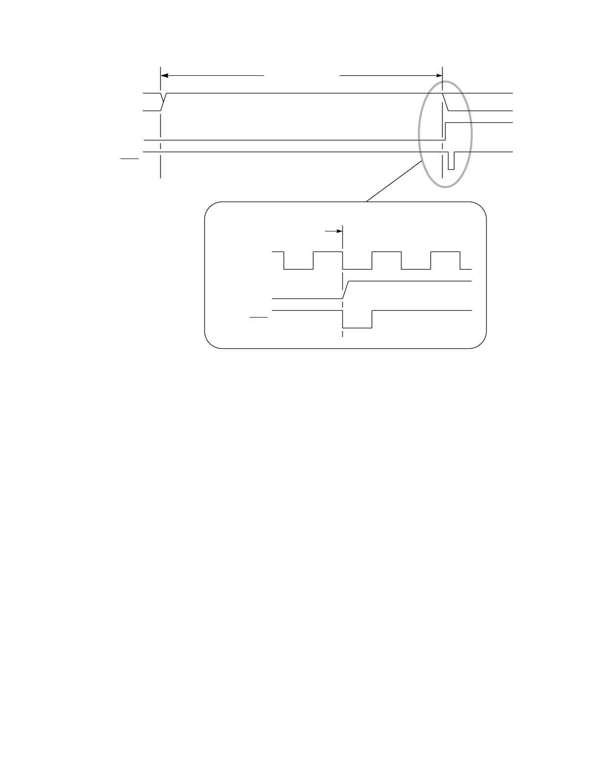
MOTOROLA ASYNCHRONOUS SERIAL COMMUNICATIONS INTERFACE M68HC11
9-36 REFERENCE MANUAL
Figure 9-16 RDRF Flag-Setting Details
PERCEIVED RxD
RDRF
[1]
PERCEIVED STOP BIT
PH2
INSET: Expanded Timing Diagram.
RDRF
XFER
[2]
[3]
XFER
PERCEIVED END
OF STOP BIT

M68HC11 MAIN TIMER AND REAL-TIME INTERRUPT MOTOROLA
REFERENCE MANUAL 10-1
SECTION 10
MAIN TIMER AND REAL-TIME INTERRUPT
This section describes the main timer system of the MC68HC11A8. Because the
clocking chains associated with the real-time interrupt and computer operating prop-
erly (COP) watch dog timer branch off the main timer counter, these timing functions
are also discussed in this section. All major clock divider chains in the microcontroller
unit (MCU) are illustrated from the oscillator to the serial baud-rate generators, which
helps put the timer counter chain in context with the rest of the MCU system.
Since the architecture of the main timer is primarily a software-driven system, several
application examples are included throughout this section. Some examples demon-
strate how to measure pulse widths and frequencies. Other examples demonstrate
techniques for controlling timer output signals. Still other examples depict how output
compares can be used for software timing.
10.1 General Description
This timer system is based on a free-running 16-bit counter with a four-stage program-
mable prescaler. A timer overflow function allows software to extend the timing capa-
bility of the system beyond the 16-bit range of the counter. Three independent input-
capture functions are used to automatically record (latch) the time when a selected
transition is detected at a respective timer input pin. Five output-compare functions are
included for generating output signals or for timing software delays. Since the input-
capture and output-compare functions may not be familiar to all users, these concepts
are explained in greater detail.
A programmable periodic interrupt circuit called the real-time interrupt (RTI) is tapped
off of the main 16-bit timer counter. Software can select one of four rates for the RTI,
which is most commonly used to pace the execution of software routines.
The computer operating properly (COP) watchdog function is loosely related to the
main timer in that the clock input to the COP system (E÷215) is tapped off the free-
running counter chain. The clocking structure for this system will be discussed briefly
in this section, but the overall COP system is explained in greater detail in SECTION
5 RESETS AND INTERRUPTS.
The timer subsystem involves more registers and control bits than any other sub-
system on the MCU. Each of the three input-capture functions has its own 16-bit time
capture latch (input-capture register) and each of the five output-compare functions
has its own 16-bit compare register. All timer functions, including the timer overflow
and RTI have their own interrupt controls and separate interrupt vectors. Additional
control bits permit software to control the edge(s) that trigger each input-capture func-
tion and the automatic actions that result from output-compare functions. Although
hardwired logic is included to automate many timer activities, this timer architecture is
essentially a software-oriented system. This structure is easily adaptable to a very

MOTOROLA MAIN TIMER AND REAL-TIME INTERRUPT M68HC11
10-2 REFERENCE MANUAL
wide range of applications although it is not as efficient as dedicated hardware for
some specific timing applications.
10.1.1 Overall Timer Block Diagram
Figure 10-1 is an overall block diagram of the main timer system. It will be helpful to
refer to this figure as the detailed explanations of the various control registers and bits
are discussed in the remainder of this section, which helps put these details in context
with the overall timer system.
The port A pin control block includes logic for timer functions and for general-purpose
I/O. For pins PA0, PA1, and PA2, this block contains edge-detection logic as well as
control logic that allows the user to select which edges will trigger an input capture.
The digital level on these pins can be read at any time (read PORTA register) even if
the pin is being used for the input-capture function. Pins PA[6:3] are used for general-
purpose output or as output-compare pins. When one of these pins is being used for
an output-compare function, it cannot be written directly as if it were a general-purpose
output. Each of the output-compare functions (OC[5:2]) is related to one of the port A
output pins. Output compare one (OC1) has extra control logic, allowing it to optionally
control any combination of the PA[7:3] pins. This extra logic is presented in 10.4.2 Ad-
vanced I/O Pin Control Using OC1. The PA7 pin can be used as a general-purpose
I/O pin, as an input to the pulse accumulator, or as an OC1 output pin.
The timer functions of these pins are discussed in detail throughout this section. In
some cases, a user may need more detailed information about the logic associated
with these pins, especially when part of port A is being used for timer I/O and the rest
is being used for general-purpose I/O. The best source for such details appears in
7.3.1 Port A, which includes complete logic diagrams for all of the port A pins.
10.1.2 Input-Capture Concept
The input-capture function is a fundamental element of the timer architecture of the
MC68HC11A8. For the MCU, physical time is represented by the count in the 16-bit
free-running counter. This counter is the central element in the main timer system. In-
put-capture functions, used to record the time at which some external event occurred,
are accomplished by latching the contents of the free-running counter when a selected
edge is detected at the related timer input pin. The time at which the event occurred is
saved in the input capture register (16-bit latch); therefore, although it may take an un-
determined variable amount of time to respond to the event, software can tell exactly
when the event occurred.
By recording the times for successive edges on an incoming signal, software can de-
termine the period and/or pulse width of the signal. To measure a period, two succes-
sive edges of the same polarity are captured. To measure a pulse width, twoalternate
polarity edges are captured. For example, to measure the pulse width for a high-going
pulse, the user would capture at a rising edge and subtract this time from the time cap-
tured for the subsequent falling edge. When the period or pulse width is less than a full
16-bit counter overflow period, the measurement is very straightforward. In practice,
software usually has to keep track of the overflows of the 16-bit counter to extend its
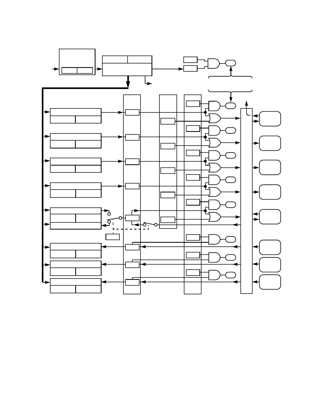
M68HC11 MAIN TIMER AND REAL-TIME INTERRUPT MOTOROLA
REFERENCE MANUAL 10-3
range.
Figure 10-1 Main Timer System Block Diagram
Another important use for the input-capture functions is to establish a time reference.
In this case, an input-capture function is used in conjunction with an output-compare
function. For example, if the user wishes to activate an output signal a certain number
of clock cycles after detecting an input event (edge), the input-capture function would
be used to record the time at which the edge occurred. A number corresponding to the
MCU
E CLK
16-BIT LATCH CLK
PA0/IC3
4
3
5
6
7
8
2
1
BIT 7
BIT 6
BIT 5
BIT 4
BIT 3
BIT 2
BIT 1
BIT 0
PORT A
PIN CONTROL
OC1I
OC2I
OC3I
OC4I
I4/O5I
IC1I
IC2I
IC3I
TFLG 1
STATUS
FLAGS
FOC1
FOC2
FOC3
FOC4
FOC5
OC1F
OC2F
OC3F
OC4F
I4/O5F
IC1F
IC2F
IC3F
PA1/IC2
PA2/IC1
PA3/OC5/
IC4/OC1
PA4/OC4/
OC1
PA5/OC3/
OC1
PA6/OC2/
OC1
PA7/OC1/
PAI
I4/O5
16-BIT COMPARATOR =
TOC1 (HI) TOC1 (LO)
16-BIT COMPARATOR =
TOC2 (HI) TOC2 (LO)
16-BIT COMPARATOR =
TOC3 (HI) TOC3 (LO)
16-BIT COMPARATOR =
TOC4 (HI) TOC4 (LO)
16-BIT LATCH
TIC1 (HI) TIC1 (LO)
CLK
16-BIT LATCH
TIC2 (HI) TIC2 (LO)
CLK
16-BIT LATCH
TIC3 (HI) TIC3 (LO)
CLK
16-BIT COMPARATOR =
TI4/O5(HI) TI4/O5 (LO)
16-BIT FREE RUNNING
COUNTER
TCNT (HI) TCNT (LO) 9
TOI
TOF
INTERRUPT REQUESTS
(FURTHER QUALIFIED BY
I BIT IN CCR)
TAPS FOR RTI,
COP WATCHDOG, AND
PULSE ACCUMULATOR
PRESCALER
DIVIDE BY
1, 4, 8, OR 16
PR1 PR0
16-BIT TIMER BUS
OC5
IC4
TO PULSE
ACCUMULATOR
TMSK 1
INTERRUPT
ENABLES
CFORC
FORCE OUTPUT
COMPARE
PIN
FUNCTIONS

MOTOROLA MAIN TIMER AND REAL-TIME INTERRUPT M68HC11
10-4 REFERENCE MANUAL
desired delay would be added to this captured value and stored to an output-compare
register. Since both input captures and output compares are referenced to the same
16-bit counter, the delay can be controlled to the resolution of the free-running counter
independent of software latencies. Details about the implementation of the input-cap-
ture functions as well as more specific examples of how to use input-capture functions
in the MC68HC11A8 are included in 10.3 Input-Capture Functions.
10.1.3 Output-Compare Concept
The output-compare function is also a fundamental element of the timer architecture
of the MC68HC11A8. For the MCU, physical time is represented by the count in the
16-bit free-running counter. This counter is the central element in the main timer sys-
tem. Output-compare functions are used to program an action to occur at a specific
time (when this 16-bit counter reaches a specific value). For each of the five output-
compare functions, there is a separate 16-bit compare register and a dedicated 16-bit
comparator. The value in the compare register is compared to the value of the free-
running counter on every bus cycle. When the compare register matches the counter
value, an output is generated, which sets an output-compare status flag and initiates
the automatic actions for that output-compare function. Optional automatic actions ini-
tiated by an output compare include generation of a hardware interrupt request and
state changes at the related timer output pin(s).
One of the easiest uses of an output-compare function is to produce a pulse of a spe-
cific duration. First, a value corresponding to the leading edge of the pulse is written
to the output-compare register. The output compare is configured to automatically set
the corresponding output either high or low, depending on the polarity of the pulse be-
ing produced. After this compare occurs, the output compare is reprogrammed to au-
tomatically change the output pin back to its inactive level at the next compare. A value
corresponding to the width of the pulse is added to the original output-compare regis-
ter value, and this result is written to the output-compare register. Since the pin-state
changes occur automatically at specific values of the free-running counter, the pulse
width can be controlled accurately to the resolution of the free-running counter inde-
pendent of software latencies. By repeating the actions for generating pulses, an out-
put signal of a specific frequency and duty cycle can be generated.
Another use of the output-compare function is to generate a specific delay. For exam-
ple, to produce a 10-ms delay to time programming of an EEPROM byte, follow the
initial programming steps to the point where the programming supply has been en-
abled (EEPGM bit has been written to one). Read the current value of the main timer
counter and add a number corresponding to 10 ms (if the count rate is 2 MHz, the val-
ue corresponding to 10 ms would be 20,00010 or $4E20). Write this sum to the output-
compare register so that an interrupt will occur when the counter gets to this value. In
this example, the actual EEPROM programming time started just before the current
time was read from the counter and ended after responding to the output compare and
turning off EEPGM. The small delays for setting up the output compare and the latency
for responding to the output compare are not considered because they only make the
EEPROM programming time longer by a few microseconds. A more advanced user of
output-compare functions will learn how to correct for these details, although it is often

M68HC11 MAIN TIMER AND REAL-TIME INTERRUPT MOTOROLA
REFERENCE MANUAL 10-5
not necessary. Details about the implementation of the output-compare functions and
specific examples of how to use output-compare functions in the MC68HC11A8 are
included in 10.4 Output-Compare Functions.
10.2 Free-Running Counter and Prescaler
The central element of the main timer system in the MC68HC11A8 is a 16-bit free-run-
ning counter. This counter starts from a count of $0000 as the MCU is coming out of
reset and then counts up continuously. When the maximum count is reached ($FFFF),
the counter rolls over to a count of $0000, sets an overflow flag, and continues to count
up. As long as the MCU is running in a normal operating mode, there is no way to re-
set, change, or interrupt the counting of this counter. This counter may be read at any
time to tell what time it is. All activities of the main timer system are referenced to this
one free-running counter; therefore, all timer functions have a known relationship to
each other.
The timer counter (TCNT) register is meant to be read using a double-byte read in-
struction such as load D (LDD) or load X (LDX). The low-order half of the counter pass-
es through a normally transparent buffer to the TCNT register. When the low-order half
of the counter is read using a single-byte read instruction, the value returned is simply
the value of the low-order eight bits of the main timer counter. When the high-order
byte of the TCNT register is read, the transparent buffer on the low-order byte of the
TCNT register is inhibited for one bus cycle. In the case of a double-byte read of
TCNT, the high-order byte is accessed first, which returns the high-order count value
and, at the same time, freezes the low-order count value buffer, which is read during
the next bus cycle. This procedure assures that the two bytes read from TCNT belong
with each other. The count value that is returned on a double-byte read corresponds
to the value of the free-running counter at the second-to-last cycle of the double-byte
read instruction. This and other subtle timing details related to the main timer are dis-
cussed in 10.5 Timing Details For The Main Timer System.
10.2.1 Overall Clock Divider Structure
The following figures, registers, and paragraphs describe the major clock divider
chains for the entire MCU system. The largest chain includes the 16-bit timer counter
and its associated prescaler. Clocks for the pulse accumulator system, RTI, and COP
watchdog branch off the main timer clocking chain. The alternative to tapping these
slower clocks off the main timer chain would have been to build additional clock divider
chains, which would have used expensive chip area. These taps off the main timer
clocking chain have special circuitry to compensate for the main timer prescaler so that
the clock frequency at these taps is independent of the prescale factor. These
postscaler circuits make it practical to share portions of the timer clocking chain in a
way that still allows the rates of the various systems to be selected independent of
TCNT — Timer Counter $100E–$100F
BIT 7 654321BIT 0
Bit 15 Bit 8 $100E
Bit 7 Bit 0 $100F
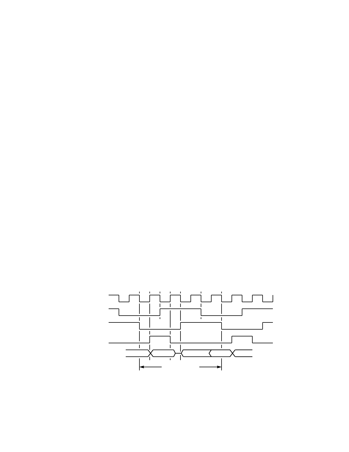
MOTOROLA MAIN TIMER AND REAL-TIME INTERRUPT M68HC11
10-6 REFERENCE MANUAL
each other.
There is a relatively complex block of logic that divides the 4 x oscillator clock down to
the internal phase 2 (PH2) clocks and the external E clock. The address strobe (AS)
signal for demultiplexing the low-order address from data is also developed in this first
oscillator divider block. Almost everything that happens inside the MCU is referenced
to the internal PH2 clocks rather than the E clock, which lags 90°behind the internal
PH2 clocks. Users who are familiar with the older MC6800 and MC6801 Families
should note that this phase shift between E and PH2 is different from what they are
used to. From an external point of view, they can still think of bus cycles as starting
and ending on falling edges of E, but they will notice a big improvement in address and
data hold times relative to this edge.
Figure 10-2 shows idealized timing relationships for the clocks and AS that are devel-
oped in the initial oscillator divider block. Since this section is devoted to the main timer
system, these clocks will not be discussed in any great detail; Figure 10-2 is presented
for reference only. For more information concerning these signals, refer to SECTION
2 PINS AND CONNECTIONS and Figure 7-12.
The logic associated with the STOP power-saving mode also contributes to the com-
plexity of the initial oscillator divider block. When the STOP mode is exited, the internal
clocks resume before the external E clock starts.
The pulse accumulator can be clocked by an external source (event counting mode)
or an internal source (time accumulation mode). The internal clocking source is an E
divided by 64 rate clock, which is tapped off of the main timer clocking chain. The pulse
accumulator is described in more detail in SECTION 11 PULSE ACCUMULATOR, but
the E divided by 64 tap is discussed in this section since it is tapped off the main timer.
The pulse accumulator tap is also used to inhibit write permission to the time-protected
control registers and bits. Certain registers and bits, such as the timer prescaler control
bits in the TMSK2 register, can only be written within the first 64 E-clock cycles after
reset.
Figure 10-2 Timing Summary for Oscillator Divider Signals
ONE BUS CYCLE
EXTAL
PH2
E
AS
ADDRESS/DATA DATA
ADDR

M68HC11 MAIN TIMER AND REAL-TIME INTERRUPT MOTOROLA
REFERENCE MANUAL 10-7
The divider chains for the serial peripheral interface (SP[) clock rate and the serial
communications interface (SCI) baud-rate generator are the last two major clock divid-
er chains in the MCU. The 4,064 bus-cycle oscillator startup delay at powerup and af-
ter STOP is derived from the SCI baud-rate counter. Like the main timer divider chain,
this divider is free running and uninterruptable except by special commands available
only in special test modes.
Figure 10-3, which illustrates all of the major clock divider chains in the
MC68HC11A8, will help the user understand how the timer fits into the overall MCU
system. The main timer counter and its prescaler and derived clock chains for RTI and
COP watchdog are described in more detail in subsequent paragraphs.
10.2.1.1 Prescaler
A programmable prescaler allows the user to select one of four clocking rates to drive
the 16-bit main timer counter. This choice allows the programmer to make a trade-off
between timer resolution and timer range. The default fastest rate causes the main
timer counter to clock at the E-clock rate, which results in a timer resolution of 500 ns
and a timer range of 32.77 ms between overflows (forE=2MHz). The slowest rate
(largest prescale factor) causes the main timer counter to clock at an E divided by 16
rate, which results in timer resolution of 8 µs and a timer range of 524.3 ms between
overflows (for E = 2 MHz).
The timer range is important because the software needed for timing functions is more
complex if timer overflows must be considered. If time periods are known to be less
than the time between successive overflows, then the overflows can be ignored, and
time periods are calculated using simple 16-bit arithmetic instructions (even if an over-
flow occurs within the timed period). The overflow from 16-bit arithmetic instructions
behaves just like an overflow from the 16-bit counter. To illustrate this point, if the timer
counter is near its maximum count ($FFF0) and an output compare is desired in 10010
cycles, add $FFF0 plus $0064 (modulo $FFFF) to get $0054 (in base ten modulo
65,536, that would be 65,520 + 100 = 84). Then write this result ($0054) to an output-
compare register. In 100 cycles, the timer counter will have overflowed and counted
up to $0054 where the output compare will occur. When overflow has to be consid-
ered, timing calculations become much more complicated.
Another factor to consider in selecting the prescaler rate is power consumption. Since
CMOS power consumption is directly proportional to its frequency of operation, power
is saved by reducing frequency. The amount of logic driven by the prescaled timer
clock is fairly small compared to the amount of logic driven by the PH2 clock, but some
savings will still result from selecting a slower count rate.
The user should consider resolution needed and the longest time period needed (or
the length of the longest pulse needed). As an example, consider measuring periods
between 10 ms and 100 ms. For an E-clock frequency of 2 MHz, a prescale division
factor of 4 would result in a timing range of 131.1 ms; therefore, overflows could be
ignored in calculations. Since the resolution would be 2 µs, an error of one count would
represent an error of 0.02 percent of the shortest expected pulse (10 ms). For most
applications, this accuracy is more than required.

MOTOROLA MAIN TIMER AND REAL-TIME INTERRUPT M68HC11
10-8 REFERENCE MANUAL
When software has to handle overflows, the latency and execution time of the overflow
service routine can become a factor in the overall accuracy of timer output functions.
For example, consider the case where an output compare coincidentally occurs short-
ly after a timer overflow. In the most straightforward approach to generating pulses
that are longer than the range of the timer counter, the output compare is not resched-
uled until after a certain number of overflows. If the output compare occurs on a very
low counter value (shortly after an overflow), the value could pass by while the over-
flow routine is being executed. Since the desired time for the output compare has al-
ready passed, the output compare is forced rather than being scheduled. Because this
forced compare is subject to software latencies rather than being strictly referenced to
the timer counter, an error will occur in the timing of the generated output signal. These
errors can be avoided by careful software treatment; however, this example demon-
strates some of the costs of using an unnecessarily small prescaler value.
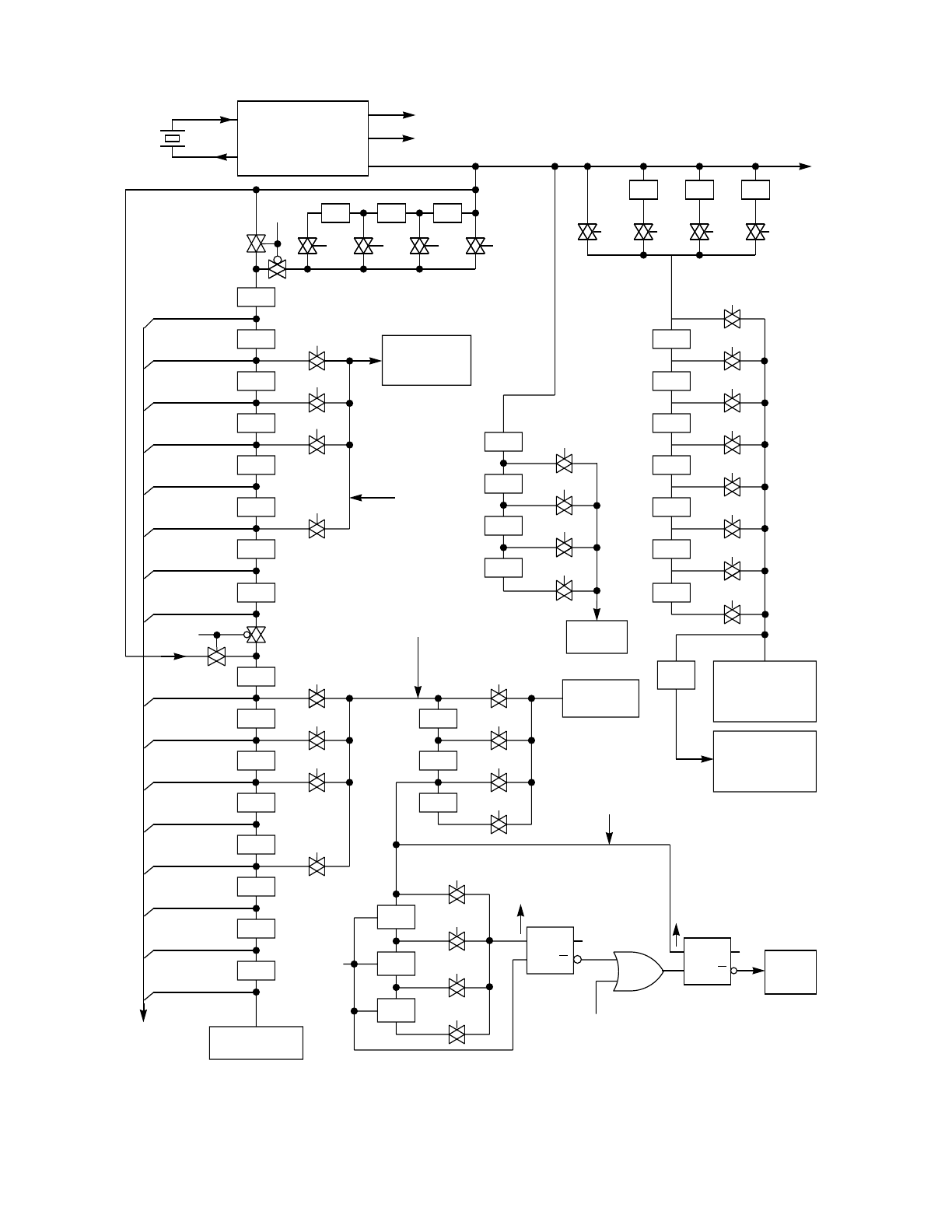
M68HC11 MAIN TIMER AND REAL-TIME INTERRUPT MOTOROLA
REFERENCE MANUAL 10-9
Figure 10-3 Major Clock Divider Chains in the MC68HC11A8
OSCILLATOR
AND
CLOCK GENERATOR
(÷4)
XTAL
EXTAL
÷2
÷21:0
÷21:1
÷2
÷2
÷2
÷21:1
0:1
÷2
÷2
÷2
÷2
÷2
÷2
÷2
÷2
÷2
TIMER
OVERFLOW
TIMER BUS
(16 BITS)
POSTSCALER
PR1:PR0
1:0
1:1
0:0
0:1
POSTSCALER
PR1:PR0
CBYP ÷2÷2÷4
0:0
PR1:PR0
0:11:01:1
EXTERNAL BUS CLOCK (E)
ADDRESS STROBE (AS)
PH2
INTERNAL BUS CLOCK (PH2)
÷3÷4÷13
0:0
SCP1:SCP0
0:1 1:0 1:1
PRESCALER
÷2
÷20:0:1
0:0:0
0:1:0
÷20:1:1
SCR2:SCR1:SCR0
÷2
÷21:0:1
1:0:0
1:1:0
÷2
÷21:1:1
÷4
÷20:1
0:0
1:0
÷21:1
SPR1:SPR0
÷2
÷2
÷20:1
0:0
1:0
÷21:1
RTR1:RTR0
0:1
1:0
÷41:1
÷4
÷4
0:0
CLEAR
COP
TIMER
SYSTEM
RESET
CR1:CR0
÷16 SCI
RECEIVE
BAUD RATE
(16X)
SCI
TRANSMIT
BAUD RATE
(1X)
SPI
BIT RATE
REAL TIME
INTERRUPT
TO PULSE
ACCUMULATOR
(E ÷ 64)
S
R
Q
Q
FF1
S
R
Q
Q
FF2
FORCE
COP
RESET
ALWAYS
E÷ 26
ALWAYS
E÷215
ALWAYS
E÷213
CBYP

MOTOROLA MAIN TIMER AND REAL-TIME INTERRUPT M68HC11
10-10 REFERENCE MANUAL
The following register and paragraphs explain the prescaler select bits, PR1 and PR0,
which are in the timer mask register 2 (TMSK2). The other bits in this register are not
related to the timer prescaler.
PR[1:0] — Timer Prescaler Select
These two bits select the prescale rate for the main 16-bit free-running timer system.
Table 10-1 shows the relationship between the prescale factor and the value of these
control bits. A prescale factor of one corresponds to an E divided by one rate for the
main timer; whereas, a prescale factor of 16 corresponds to a timer count rate of E
divided by 16. In normal modes, this prescale rate can only be changed once within
the first 64 bus cycles after reset, and the resulting count rate stays in effect until the
next reset.
10.2.1.2 Overflow
In cases where periods greater than the range of the timer counter have to be mea-
sured or produced, the timer overflow must be used, which is similar to measuring
times greater than 60 seconds by using the seconds display of a digital clock. The
minute and hour displays can be thought of as software counters, which extend the
range of the seconds counter. Each time the seconds counter overflows (goes from 59
to 0), the minutes counter is incremented. If a period less than 60 seconds is desired,
add (modulo 60) the desired number of seconds to the starting time to get the ending
time.
In the MC68HC11A8, the timer overflow flag (TOF) status bit is set each time the timer
counter overflows from $FFFF to $0000. This bit can optionally generate an automatic
interrupt request each time it is set by setting the timer overflow interrupt (TOI) enable
bit in the timer mask register 2 (TMSK2). Software must acknowledge that it has seen
the overflow condition by clearing the TOF status indicator. The free-running counter
continues to run even if the TOF status indicator is not cleared. If overflow indications
are not important to a particular application, they may be ignored. The following regis-
ters and paragraphs describe the TOF status bit and the TOI interrupt enable. The oth-
TMSK2 — Timer Interrupt Mask Register 2 $1024
BIT 7 654321BIT 0
TOI RTII PAOVI PAII 0 0 PR1 PR0
RESET: 00000000
Table 10-1 Crystal Frequency vs. PR1, PR0 Values
PR1 PR0 Prescale Fac-
tor
Crystal Frequency
223 Hz 8 MHz 4 MHz
One Count (Resolution)/Overflow (Range)
0
1
1
1
0
0
0
1
1
4
8
16
477 ns/31.25 ms
191 µs/125 ms
3.81 µs/250 ms
7.63 µs/.05 s
500 ns/32.77 ms
2µs/131.1 ms
4µs/62.1 ms
8µs/524.3 ms
1µs/65.54 ms
4µs/262.1 ms
8µs/524.3 ms
16 µs/1.049 s
2.1 MHz 2 MHz 1 MHz
Bus Frequency (E Clock)

M68HC11 MAIN TIMER AND REAL-TIME INTERRUPT MOTOROLA
REFERENCE MANUAL 10-11
er bits in these registers are not associated with the timer overflow.
TOI, TOF — Timer Overflow Interrupt Enable, Timer Overflow Flag
The TOF status bit is automatically set to one each time the free-running 16-bit counter
rolls over from $FFFF to $0000. This status bit is cleared by writing to the TFLG2 reg-
ister with a one in the corresponding data bit position (bit 7). The TOI control bit allows
the user to configure the timer overflow for polled or interrupt-driven operation but
does not affect the setting or clearing of the TOF bit. When TOI is zero, timer overflow
interrupts are inhibited, and the timer overflow is operating in a polled mode. In this
mode, the TOF bit must be polled (read) by user software to determine when an over-
flow has occurred. When the TOI control bit is one, a hardware interrupt request is
generated whenever the TOF bit is set to one. Before leaving the interrupt service rou-
tine, software must clear the TOF bit by writing to the TFLG2 register (see 10.2.4 Tips
for Clearing Timer Flags).
10.2.1.3 Counter Bypass (Test Mode)
In special modes of operation (test and bootstrap), there is a counter bypass function
to simplify testing of the main timer functions. This function is activated by writing a one
to the counter bypass (CBYP) control bit in the TEST1 control register, which can only
be written in the special modes. When CBYP is one, the main timer counter is recon-
figured so that the prescaler is bypassed and the upper and lower halves of the 16-bit
counter are simultaneously driven by the internal PH2 clock. This dramatically reduces
testing time for the main timer.
The functions that are tapped off of the main timer would have erroneous timing while
the CBYP function is enabled. Since this configuration is only possible in special test
modes, it does not interfere with any use of the systems in normal modes.
10.2.2 Real-Time Interrupt (RTI) Function
The RTI function can be used to generate hardware interrupts at a fixed periodic rate.
A common software practice is to organize the routines that compose the software for
an application into a sequence of major subroutine calls. The length of time required
to execute all of the routines is a variable, which depends upon how much each routine
had to do, but the worst-case time to execute the entire sequence of routines should
be known. After completing a pass through all the routines, software enters a delay
mode until a time reference signal is detected. Upon detecting this signal, a jump is
TMSK2 — Timer Interrupt Mask Register 2 $1024
BIT 7 654321BIT 0
TOI RTII PAOVI PAII 0 0 PR1 PR0
RESET: 00000000
TFLG2 — Timer Interrupt Flag Register 2 $1025
BIT 7 654321BIT 0
TOF RTIF PAOVF PAIF 0000
RESET: 00000000

MOTOROLA MAIN TIMER AND REAL-TIME INTERRUPT M68HC11
10-12 REFERENCE MANUAL
performed to the top of the sequence, and all the subroutines are again executed in
sequence. By knowing the time between successive time reference signals, a routine
can measure real time by noting the number of times it is executed and multiplying by
the time between successive time reference signals (in this case, the RTI period).
In the MC68HC11A8, the RTI system can be used to provide this periodic time refer-
ence signal. To accommodate the needs of a variety of applications, four different
rates are available for the RTI signal. These rates are a function of the MCU oscillator
frequency and the value of two software-accessible control bits (RTR1 and RTR0). Al-
though the rate can be changed at any time, it is typically established shortly after reset
and left alone.
The clock source for the RTI function is a free-running clock that cannot be stopped or
interrupted. This clock causes the time between successive RTI time-outs to be a con-
stant, which is independent of the software latencies associated with flag clearing and
service. Thus, an RTI period starts from the previous RTI time-out, not from when RTIF
is cleared.
The most common problem users encounter with the RTI system is that they forget to
clear RTIF after it is recognized. If the flag is not cleared by a specific software write
to the TFLG2 register, it will already be pending the next time it is checked. If the sys-
tem is being used in an interrupt-driven mode, the interrupt will be requested and ser-
viced immediately after the return from interrupt (RTI) instruction is executed at the
end of the RTI service routine. This sequence results in a system lockup where the
RTI service routine is executed continuously to the exclusion of all else. The only way
out of this infinite loop is a system reset. If the RTI system is operating in a polled
mode, the main routine sequence will operate correctly the first time and wait until
RTIF is set the first time. As soon as RTIF is set, the jump is executed back to the top
of the sequence as expected. The routines will be executed the second time and soft-
ware should wait for the end of the next RTI period, but, since RTIF is still set, software
thinks the RTI period has already expired. The result will be that the main sequence is
repeated too quickly.
The following registers and paragraphs explain the RTI flag and RTI enable. The other
bits in these registers are not related to the RTI system.
RTII, RTIF — Real-Time Interrupt Enable, Real-Time Interrupt Flag
The RTIF status bit is automatically set to one at the end of every RTI period. This sta-
TMSK2 — Timer Interrupt Mask Register 2 $1024
BIT 7 654321BIT 0
TOI RTII PAOVI PAII 0 0 PR1 PR0
RESET: 00000000
TFLG2 — Timer Interrupt Flag Register 2 $1025
BIT 7 654321BIT 0
TOF RTIF PAOVF PAIF 0000
RESET: 00000000

M68HC11 MAIN TIMER AND REAL-TIME INTERRUPT MOTOROLA
REFERENCE MANUAL 10-13
tus bit is cleared by writing to the TFLG2 register with a one in the corresponding data
bit position (bit 6). The RTII control bit allows the user to configure the RTI system for
polled or interrupt-driven operation but does not affect the setting or clearing of RTIF.
When RTII is zero, interrupts are inhibited, and the RTI system is operating in a polled
mode. In this mode, the RTIF bit must be polled (sampled) by user software to deter-
mine when an RTI period has elapsed. When the RTII control bit is one, a hardware
interrupt request is generated each time RTIF is set to one. Before leaving the interrupt
service routine, software must clear RTIF by writing to the TFLG2 register (see 10.2.4
Tips for Clearing Timer Flags).
The following register and paragraphs explain the RTI rate select bits in the pulse ac-
cumulator control register (PACTL). The other bits in this register are not related to the
RTI system.
RTR1, RTR0 — Real-Time Interrupt Rate Selects
These two bits determine the rate at which interrupts will be requested by the RTI sys-
tem. The RTI system is driven by an E divided by 213 rate clock compensated so that
it is independent of the timer prescaler. These two control bits select an additional di-
vision factor. Table 10-2 shows the RTI rates that result for various combinations of
crystal frequency and RTI rate-select control bit values. RTI is set to its fastest rate by
default out of reset and may be changed at any time.
10.2.3 COP Watchdog Function
The COP watchdog function is only superficially related to the main timer system. The
clocking chain for the watchdog function is tapped off of the main timer divider chain.
Figure 10-3 illustrates how the COP clock is derived from the main timer clocking
chain. Although the COP clocking chain is discussed briefly, the COP system is ex-
plained in greater detail in SECTION 5 RESETS AND INTERRUPTS.
The counter stages up to the E divided by 215 tap have no reset input; whereas, the
divider stages after this tap are reset each time the COP clearing sequence is execut-
PACTL — Pulse Accumulator Control $1026
BIT 7 654321BIT 0
DDRA7 PAEN PAMOD PEDGE 0 0 RTR1 RTR0
RESET: 00000000
Table 10-2 RTI Rates vs. RTR1, RTR0 for Various Crystal Frequencies
RTR1 RTR0 E÷213 Divided By
Crystal Frequency
223 Hz 8 MHz 4 MHz
Nominal RTI Rate
0 0 1 3.91 ms 4.10 ms 8.19 Ms
0 1 2 7.81 ms 8.19 Ms 16.38 ms
1 0 4 15.62 ms 16.38 ms 32.77 ms
1 1 8 31.25 ms 32.77 ms 65.54 ms
2.1 MHz 2 MHz 1 MHz
Bus Frequency (E Clock)

MOTOROLA MAIN TIMER AND REAL-TIME INTERRUPT M68HC11
10-14 REFERENCE MANUAL
ed (see Figure 10-3). This structure determines the uncertainty of the COP time-out
period because software has no practical way of knowing when the first clocking edge
will appear at the E divided by 215 tap relative to the COP clearing sequence. For a
bus frequency of 2 MHz (E), the first clock can appear at the E divided by 215 tap any-
where between ~0 to 16.4 ms after a COP clearing sequence. This tolerance or un-
certainty depends on the bus frequency (E) but does not vary with respect to the rate
selects (CR1, CR0).
The following register and paragraphs explain the COP timer rate select bits located
in the options control register (OPTION). The other bits in this register are not related
to the main timer system or the COP system.
CR1, CR0 — COP Timer Rate Select Bits
The MCU internal E clock is first divided by 215 before it enters the COP watchdog sys-
tem. The CR1 and CR0 control bits regulate a further scaling factor for the watchdog
timer as shown in Table 10-3. The columns at the right of the table show the resulting
watchdog time-out periods for three typical oscillator frequencies. After reset, the time-
out period is configured for the shortest time-out period by default. In normal operating
modes, these bits can only be written once, and that write must be within 64 bus cycles
after reset.
10.2.4 Tips for Clearing Timer Flags
The most common method of clearing a status flag bit in the timer flag registers is to
load an accumulator with a mask that has a one in the bit(s) corresponding to the
flag(s) to be cleared; then write this value to TFLG1 or TFLG2. A bit clear (BCLR) in-
struction can also be used to clear a flag in TFLG1 or TFLG2. The mask, which is sup-
plied with the BCLR instruction, should have zeros in the bit positions corresponding
to the flags to be cleared and ones in all other bits. To clear the TOF flag, execute
BCLR TFLG2 with a mask of %01111111. The BCLR instruction will read TFLG2, AND
it with the inverse of the supplied mask (%10000000 in this case), and write the result
OPTION — System Configuration Options $1039
BIT 7 654321BIT 0
ADPU CSEL IRQE DLY CME 0 CR1 CR0
RESET: 00000000
Table 10-3 COP Time-Out vs. CR1, CR0 Values
CR1 CR0 E÷ 215 Divided
By
Crystal Frequency
223 Hz 8 MHz 4 MHz
Nominal Time-Out
0 0 1 15.625 ms 16.384 ms 32.768 ms
0 1 4 62.5 ms 65.536 ms 131.07 ms
1 0 16 250 ms 262.14 ms 524.29 ms
1 1 64 1 s 1.049 s 2.1 s
2.1 MHz 2 MHz 1 MHz
Bus Frequency (E Clock)

M68HC11 MAIN TIMER AND REAL-TIME INTERRUPT MOTOROLA
REFERENCE MANUAL 10-15
back to TFLG2. The condition of the other flags in the register is not important, even if
they become set in the middle of the BCLR instruction, because the write cycle of the
instruction will write zeros to all bits except those corresponding to flags that are to be
cleared. Writing a zero to a bit corresponding to a flag that is set does not disturb the
flag.
It is not appropriate to use the bit set (BSET) instruction to clear flags in the timer flag
registers because this could inadvertently clear one or more of the other flags in the
register. Again, consider the case of clearing the TOF bit. Suppose RTIF is set after
the TOF interrupt is recognized but before the BSET instruction is started. The BSET
instruction is a read-modify-write instruction that reads the operand, ORs this with a
mask having ones in the bit(s) to be set, and writes the resulting value back to the op-
erand address. Using this instruction on TFLG1 or TFLG2 will clear all flags that are
set at the time the operand (in this case, the TFLG2 register) is read.
There are many instruction sequences that can be used to clear timer flags. In general,
each sequence takes a different number of bytes of object code and a different number
of cycles of execution time. The best sequence depends on a number of factors, in-
cluding (but not limited to) whether the user wants minimum execution time or mini-
mum program memory space. In many cases, the subtle differences in program size
and execution time are unimportant, and any of the sequences shown would be equal-
ly acceptable. Some sequences require registers to be in the direct addressing mode
memory space ($0000–$00FF), which is not practical in many applications. Since oth-
er sequences use indexed addressing, their efficiency will depend on whether or not
the index register already points to the register space (extra instructions and time are
required if the index register has to be changed). Table 10-4 illustrates seven different
instruction sequences that could be used to clear the TOF status bit in TFLG2.
10.3 Input-Capture Functions
Each input-capture function includes a 16-bit latch, input edge-detection logic, and in-
terrupt generation logic. The 16-bit latch captures the current value of the free-running
counter when a selected edge is detected at the corresponding timer input pin. The
Table 10-4 Instruction Sequences To Clear TOF
Instruction
Sequence Opcode Operand(s) Address
Mode Bytes Cycles Total Sequence
Bytes Cycles
1LDAA
STAA #$80
<TFLG2 (IMM)
(DIR) 2
22
345
2 BCLR <TFLG2 $7F (DIR) 3636
3LDAA
STAA #$80
TFLG2 (IMM)
(EXT) 2
32
456
4LDAA
STAA #$80
TFLG2,X (IMM)
(IND,X) 2
22
446
5 BCLR TFLG2,X $7F (IND,X) 3737
6LDAA
STAA #$80
TFLG2,Y (IMM)
(IND,Y) 2
32
557
7 BCLR TFLG2,Y $7F (IND,Y) 4848

MOTOROLA MAIN TIMER AND REAL-TIME INTERRUPT M68HC11
10-16 REFERENCE MANUAL
edge-detection logic includes control bits so that user software can select the edge po-
larity that will be recognized. Each of the three input-capture functions can be indepen-
dently configured to detect rising edges only, falling edges only, or any edge (rising or
falling). The interrupt generation logic includes a status flag, which indicates that an
edge has been detected, and a local interrupt enable bit, which determines whether or
not the corresponding input-capture function will generate a hardware interrupt re-
quest. If the interrupt request is inhibited, the input capture is operating in polled mode
where software must read the status flag to recognize that an edge was detected.
Input-capture edges are generally asynchronous to the internal timer counter, which
is clocked relative to the PH2 clock. These asynchronous capture requests are then
synchronized to PH2 so that the actual latching will occur on the opposite half cycle of
PH2 from when the timer counter is being incremented. This synchronization process
introduces a delay from when the actual edge occurs to when the counter value is
latched. In almost all cases, this very short delay should be ignored. When the time
between two edges is being measured, both edges are subject to the same delay;
therefore, these delays will offset each other. When an input capture is being used in
conjunction with an output compare, there will be a similar delay between the actual
compare point and when the output pin actually changes state. When a prescale factor
other than one is being used, the capture delay is smaller than the uncertainty due to
timer resolution. Detailed information about timer system delays is given in 10.5 Tim-
ing Details For The Main Timer System. The central element of each input-capture
function is the input-capture latch, which can be read by software as a pair of 8-bit reg-
isters (see the following input-capture registers). The TLCx registers are not affected
by reset and cannot be written by software. When an edge has been detected and syn-
chronized, the 16-bit free-running counter value is transferred into the input-capture
register pair as a single 16-bit parallel transfer. Timer-counter value captures and tim-
er-counter incrementing occur on opposite half cycles of the PH2 clock so that the
count value is stable whenever a capture occurs. The input-capture functions operate
independently of each other, and all three functions can capture the same 16-bit count
value if the input edges are all detected within the same timer count cycle.
A read of the high-order byte of an input-capture register pair inhibits a new capture
transfer for one bus cycle. As long as a double-byte read instruction such as load D
(LDD) is used to read input-capture values, the user is assured that the two bytes be-
long with each other. If a new input-capture occurs so that a transfer would have oc-
curred immediately after the high-byte read, it will be delayed for one more cycle but
will not be lost.
Bit 7 654321Bit 0
$1010 Bit 15 ——————Bit 8 TIC1
$1011 Bit 7 ——————Bit 0
$1012 Bit 15 ——————Bit 8 TIC2
$1013 Bit 7 ——————Bit 0
$1015 Bit 7 ——————Bit 0

M68HC11 MAIN TIMER AND REAL-TIME INTERRUPT MOTOROLA
REFERENCE MANUAL 10-17
The latching action of an input-capture function occurs every time a selected edge is
detected on the corresponding timer input pin (even if the corresponding input-capture
flag is already set). This means that the value read from the input-capture register cor-
responds to the most recent edge at the pin, which may not be the edge that caused
the input-capture flag to be set. In a few applications, there could be a number of close-
ly spaced edges (i.e., an unfiltered bouncing switch contact). In cases where these ex-
tra captures are undesirable, software can write to the edge-select control bits to
inhibit further captures until after the current capture has been handled.
The following registers and paragraphs explain the input-capture status flags and the
local interrupt enable control bits for the input-capture functions.
ICxI, ICxF — Input Capture Interrupt Enables and Input Capture Flags (x = 1, 2, or 3)
The ICxF status bit is automatically set to one each time a selected edge is detected
at the corresponding input-capture pin. This status bit is cleared by writing to the
TFLG1 register with a one in the corresponding data bit position. The ICxI control bit
allows the user to configure each input-capture function for polled or interrupt-driven
operation but does not affect the setting or clearing of the corresponding ICxF bit.
When ICxI is zero, the corresponding input-capture interrupt is inhibited, and the input
capture is operating in a polled mode. In this mode, the ICxF bit must be polled (read)
by user software to determine when an edge has been detected. When the ICxI control
bit is one, a hardware interrupt request is generated whenever the corresponding ICxF
bit is set to one. Before leaving the interrupt service routine, software must clear the
ICxF bit by writing to the TFLG1 register (see 10.2.4 Tips for Clearing Timer Flags).
10.3.1 Programmable Options
The user can program each input-capture function to detect a particular edge polarity
on the corresponding timer input pin. A pair of control bits (EDGXB, EDGxA) in the tim-
er control register 2 (TCTL2) are used to select the edge(s) detected by each input-
capture function.
TMSK1 — Timer Interrupt Mask 1 Register $1022
BIT 7 654321BIT 0
OC1I OC2I OC3I OC4I OC5I IC1I IC2I IC3I
RESET: 00000000
TFLG1 — Timer Interrupt Flag 1 Register $1023
BIT 7 654321BIT 0
OC1F OC2F OC3F OC4F OC5F IC1F IC2F IC3F
RESET: 00000000
TCTL2 — Timer Control Register $1021
BIT 7 654321BIT 0
0 0 EDG1B EDG1A EDG2B EDG2A EDG3B EDG3A
RESET: 00000000

MOTOROLA MAIN TIMER AND REAL-TIME INTERRUPT M68HC11
10-18 REFERENCE MANUAL
EDGxB, EDGxA — Input Capture Edge Control (x = 1, 2, or 3)
These pairs of bits determine which edge(s) the input-capture functions will be sensi-
tive to. These bit pairs are encoded as shown in the following table:
10.3.2 Using Input Capture to Measure Period and Frequency
Timer Examples 10–1(a) and 10–1(b) show how to measure a period using an input-
capture function. A complete assembly listing for all timer section examples is shown
in 10.6 Listing of Timer Examples. Timer Example 10–1(a) measures the time be-
tween two successive rising edges on an input signal at the PA2/IC1 pin. This program
uses the input-capture function in polled mode for demonstration because it is a little
simpler than the interrupt-driven operation. Other examples in this section will demon-
strate interrupt-driven operation, which is often a more flexible approach because the
MCU can be performing other tasks while waiting for a particular timer event.
Example 10–1(b) changes the period obtained from Example 10–1(a) into a frequency
to display the results in a more familiar form. Also, support routines are provided to
convert hexadecimal numbers into decimal numbers. When running the example, a
period is measured at the IC1 pin and displayed as a decimal period (in E cycles) and
as a frequency (in Hz). After printing the result, the program returns to its start and re-
peats continuously. Depending on the display-device speed and the signal at IC1, a
screen can be filled with results very quickly. To stop, just press the reset button on
the EVB board.
Figure 10-4 shows the critical instructions in the measurement of the period of the sig-
nal at the PA2/IC1 pin. The numbers in square brackets in the listings indicate the
number of MCU E cycles needed to execute each instruction. This information is used
in the timing analysis presented in Figure 10-5.
The timing analysis for Example 10–1 is shown in Figure 10-5, which is very detailed
to show exactly what occurs in an input capture. Software instructions are used to read
the first captured value, to prepare for the second capture, and to reset the input-cap-
ture flag. These instructions require a finite amount of time. If the period of the signal
being measured is too short, the second edge can come before the program is ready
for it. This period will determine the highest frequency that can be measured with this
example program. If the signal period being measured is longer than the range of the
16-bit timer counter, then two periods, which are exactly one overflow time apart, are
not distinguishable. Since this program does not consider overflows, this period will
determine the lowest frequency that can be measured with this program. These limi-
tations are program limits, and, as shown in other examples, the input-capture func-
tions can be used to measure much shorter or much longer periods.
EDGxB EDGxA Configuration
0 0 Capture Disabled
0 1 Capture on Rising Edges Only
1 0 Capture on Falling Edges Only
1 1 Capture on Any Edge (Rising or Falling)
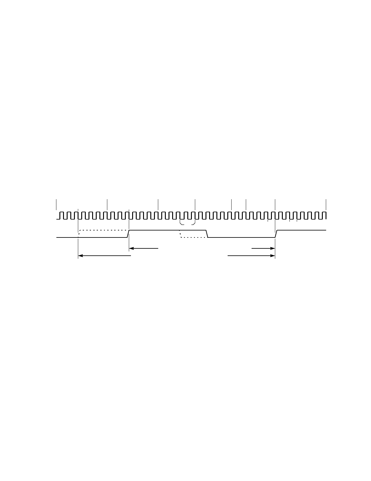
M68HC11 MAIN TIMER AND REAL-TIME INTERRUPT MOTOROLA
REFERENCE MANUAL 10-19
* Ready to detect first rising edge
c00e 1f 23 04 fc[7] BRCLR TFLG1,X $04 *Loop here until edge
* First edge detected
c012 ec 10 [5] LDD TIC1,X Read time of first edge
c014 fd d00d [5] STD FRSTE Save first capture value
c017 86 04 [2] LDAA #$04
c019 a7 23 [4] STAA TFLG1,X Clear IC1F before next edge
* Ready to capture time of second edge
c01b 1f 23 04 fc[7] BRCLR TFLG1,X $04 *Loop here until edge
* Second edge detected
c01f ec 10 [5] LDD TIC1,X Read time of second edge
c021 b3 d0 0d [6] SUBD FRSTE 2nd - 1st -> D
c024 fd d0 0f [5] STD PERC Save result (period in cycles)
Figure 10-4 Measuring a Period with Input Capture
Figure 10-5 Timing Analysis for Example 10–1
As shown in Example 10–1(a), the CPU repeats the BRCLR instruction continuously,
waiting for the first rising edge. Since the edge is asynchronous to the program exe-
cution, where the edge will occur relative to this program is uncertain. This uncertainty
leads to a best-case and a worst-case minimum period that can be measured by this
program. The worst case arises if the edge is detected too late to be seen by the
BRCLR instruction at [1]. The best case arises when the edge is detected in time to be
seen by the BRCLR instruction at [2]. From the cycle-by-cycle description of the
BRCLR instruction, the read of the operand (TFLG1 register in this case) is shown to
occur in the third cycle of the instruction. The captured value is read during the last two
cycles of the LDD instruction at [3], and the IC1F status flag is cleared during the last
cycle of the STAA TFLG1,X instruction at [4]. Although a new capture could occur be-
tween [3] and [4], it would be cleared by the STAA at [4] and would not be recognized
by the program. The earliest place the second edge could occur and be properly han-
dled is during the cycle after the status flag clear instruction [4].
This timing analysis is based on a detailed knowledge of timer logic and instruction tim-
BEST CASE MINIMUM PERIOD (20 CYCLES)
E
IC1
PIN
BRCLR TFLG1,X $04∗LDAA
#$04
LDD TIC1,XBRCLR TFLG1,X $04∗STD FRSTE STAA
TFLG1,X BRCLR TFLG1,X $04∗
[1] [2] [3] [4] [5]
WORST CASE MINIMUM PERIOD (27 CYCLES)

MOTOROLA MAIN TIMER AND REAL-TIME INTERRUPT M68HC11
10-20 REFERENCE MANUAL
ing. Instruction timing tells which cycle within the instruction actually reads or writes a
register. Instruction details can be found in APPENDIX A INSTRUCTION SET DE-
TAILS. Detailed information concerning timer captures is given in 10.5 Timing Details
For The Main Timer System. For most applications, it is not necessary to study the
timing in this much detail, but at least one detailed example should be studied.
Example 10–1(b), which converts the period from Example 10–1(a) into frequency, is
more of a demonstration of FDIV and XGDX than anything else. In a real application,
the user would normally work with the period value rather than converting it to a fre-
quency. Some shortcuts were taken since the results were not that critical. For exam-
ple, the partial sums were truncated rather than rounding or extending the precision of
the calculations. Although these shortcuts lead to small errors in the results, these er-
rors were not important, considering the resolution of the measurements. To measure
the frequency of an incoming signal, a user could accumulate the time of many cycles
of the signal and calculate an average period, which would yield much finer resolution
than the single-cycle measurement taken in Example 10–1.
After working with the timer and pulse accumulator for a while, a good exercise might
be to develop a way to measure the signal frequency to five digits of accuracy. The
following discussion presents a proposed technique that could be tried, although it has
not been proven. First, connect the signal to the pulse accumulator input and to an in-
put-capture input. Capture the time of a first edge and start the pulse accumulator at
a count of 256 minus 200. While waiting for 199 cycles of the incoming signal, monitor
timer overflows, like Example 10–3 does, because 200 cycles of the signal are very
likely to take longer than one timer overflow. When the pulse accumulator has counted
199 cycles of the signal, clear the input-capture flag and wait for a capture of the time
of the 200th cycle. From the number of overflows and the difference between the final
capture value and the first capture value, the user can determine the period of 200 cy-
cles of the incoming signal. Finally, convert this into frequency. The accuracy is basi-
cally one E cycle in 200 cycles of the signal, which corresponds to about ±1Hzat20
kHz, and the accuracy improves for lower frequencies. For very low frequencies, it is
not necessary to measure many periods to get the accuracy. Try to include a prelimi-
nary trial measurement to decide how many cycles should be measured to get the
needed accuracy (auto ranging).
10.3.3 Using Input Capture to Measure Pulse Width
Timer Example 10–2 shows how to measure a pulse width with an input capture, which
is almost the same as measuring a period, except that the input-capture edge sensi-
tivity must be reconfigured between the capture of the first edge and the second edge.
Since this particular program measures the period of a high-going pulse, the input cap-
ture is first configured to capture on a rising edge at the input. After detecting the first
edge, the input capture is reconfigured to detect a falling edge.
Since this program is interrupt driven, it must have an interrupt service routine, which
is automatically called as a result of an interrupt, an initialization portion, and a main-
line program portion. Since this example is only demonstrating the input-capture func-
tion, the mainline program will be a trivial two-instruction loop that repeats until a pulse
has been measured. In a practical application, the mainline portion would be every-

M68HC11 MAIN TIMER AND REAL-TIME INTERRUPT MOTOROLA
REFERENCE MANUAL 10-21
thing other than initialization and interrupt service routines.
This example is intended to run on an M68HC11EVB evaluation board; thus, the inter-
rupt vector will be treated in a somewhat unusual way. The actual interrupt vector for
input capture 1 is at $FFEE and $FFEF, which is in the monitor program EPROM on
the EVB board. To allow use of these vectors, they have been initialized to point at
specific RAM locations called pseudo-vectors. To use a vector, put a jump (JMP) in-
struction to the address of the interrupt service routine at the RAM pseudo-vector lo-
cations ($00E8, E9, and EA for timer input-capture 1).
In a normal application, the address of the service routine would be hard coded into
the double-byte vector location rather than writing a jump instruction into RAM during
initialization. For additional information about interrupts, see SECTION 5 RESETS
AND INTERRUPTS.
The partial listing shown in Figure 10-6 depicts the important parts of the pulse-width
measurement illustrated in Example 10–2.
A detailed timing analysis for Example 10–2 is shown in Figure 10-7. Unlike the pre-
vious example, interrupt latencies must be considered to determine the minimum
pulse width that can be measured by this program. The instructions in the main pro-
gram do not affect the minimum measurable pulse except that the execution time of
the longest instruction executing at the time of the interrupt determines the longest
possible latency from an input-capture edge to when it can be serviced. The interrupt
operation does not begin until the currently executing instruction is completed. If the
pulse width being measured is too short, the second edge can come before the pro-
gram is ready for it. This time will determine the shortest pulse that can be measured
with this example program. As in the previous example, if the signal being measured
is longer than the range of the 16-bit timer counter, then two pulse widths, which were
different by an exact multiple of the overflow period, are not distinguishable. Since this
program does not consider overflows, the overflow period of the 16-bit timer will deter-
mine the longest pulse that can be measured correctly with this program. These limi-
tations are program limits and, as shown in other examples, the input-capture
functions can be used to measure much shorter or much longer times.
As shown in Example 10–2, the CPU repeats the WAITL2 loop continuously, waiting
for the first rising edge. Since the edge is asynchronous to the program execution,
where the edge will occur relative to this program is uncertain. This uncertainty leads
to a best-case and a worst-case minimum period that can be measured by this pro-
gram. The worst case arises when the first edge is not recognized before the end of
the BEQ WAITL2 instruction at [1]. In this worst case, the LDAA IC1DUN instruction
would have to finish, which causes an extra four-cycle delay. The best case arises
when the edge is recognized just before the end of an instruction in the main program.
In this best case, interrupt processing starts almost immediately. A more obscure pos-
sibility would exist if there were other lower priority interrupts enabled in the system.
In that case, a lower priority interrupt could initiate stacking leading to the interrupt. The
priority resolution to decide which vector to take does not occur until the stacking op-
erations are finished. If the IC1 edge is recognized before the condition code register
(CCR) is stacked, it will be serviced rather than the lower priority interrupt that started

MOTOROLA MAIN TIMER AND REAL-TIME INTERRUPT M68HC11
10-22 REFERENCE MANUAL
the interrupt process. In this unusual case, the best-case minimum response could be
much shorter. This case does not arise in Example 10–2 because no lower priority in-
terrupts are enabled.
*** initialization - (see full listing) ***
c09c ce 10 00 [3] PWTOP LDX #REGBAS Point to register block
c09f 86 10 [2] LDAA #%00010000 EDG1B:EDG1A - 0:1
c0a1 a7 21 [4] STAA TCTL2,X IC1 rising edges
c0a3 86 ff [2] LDAA # $FF
c0a5 b7 d0 06 [4] STAA IC1MOD FF-off; 0-lst edge; 1-last edge
c0a8 7f d0 05 [6] CLR IC1DUN Signal pulse not done
c0ab 1d 23 fb [7] SCLR TFLG1,X $FB clear IC1F (if any)
c0ae 1c 22 04 [7] BSET TMSK1,x $04 enable IC1 interrupts
c0b1 0e [2] CLI Enable Interrupts
c0b2 b6 d0 05 [4] WAITL2 LDAA IC1DUN Sets after pulse done
c0b5 27 fb [3] BEQ WAITL2 Loop till pulse has been timed
c0b7 0f [2] SEI Pulse done, disable interrupts
*** display results - (see full listing)
***
* SV2IC1 - Input Capture 1 service routine
*
* Called first when a rising edge is detected and again
* when a falling edge is detected.
***
c0d8 ce 10 00 [3] SV2IC1 LDX #REGBAS point at top of register block
c0db 7c d0 06 [6] INC IC1MOD $FF->0 at 1st edge; 0->1 at 2nd
c0de 26 0d [3] BNE NO1ST2 if not 0, this is trailing edge
* Process leading edge of pulse
c0e0 ec 10 [5] LDD TIC1X read time of first edge
c0e2 fd d0 0d [5] STD FRSTE save till next capture
* Reconfigure IC1 for trailing falling edge
c0e5 1d 21 30 [7] BCLR TCTL2,X $30 EDG1B:EDG1A->0:0
c0e8 1c 21 20 [7] BSET TCTL2,X $20 EDG1B:EDG1A->1:0
c0eb 20 10 [3] BRA OU2IC1 done processing first edge
* Process trailing edge of pulse
c0ed ec 10 [5] NO1ST2 LDD TIC1,X got time of trailing edge
c0ef b3 d0 0d [6] SUBD FRSTE (time of last) - (time of 1st)
c02f dd 01 5 [5] STD HPW update result
c0f5 1d 21 30 [7] BCLR TCTL2,X $30 disable IC1
c0f8 86 01 [2] LDAA #1
c0fa b7 d0 05 [4] STAA IC1DUN signal pulse measured
c0fd 1d 23 fb [7] OU2IC1 BCLR TFLG1,X $FB clear IC1F
c100 3b [12] RTI ** Return from IC1 service
Figure 10-6 Measuring a Pulse Width with Input Capture
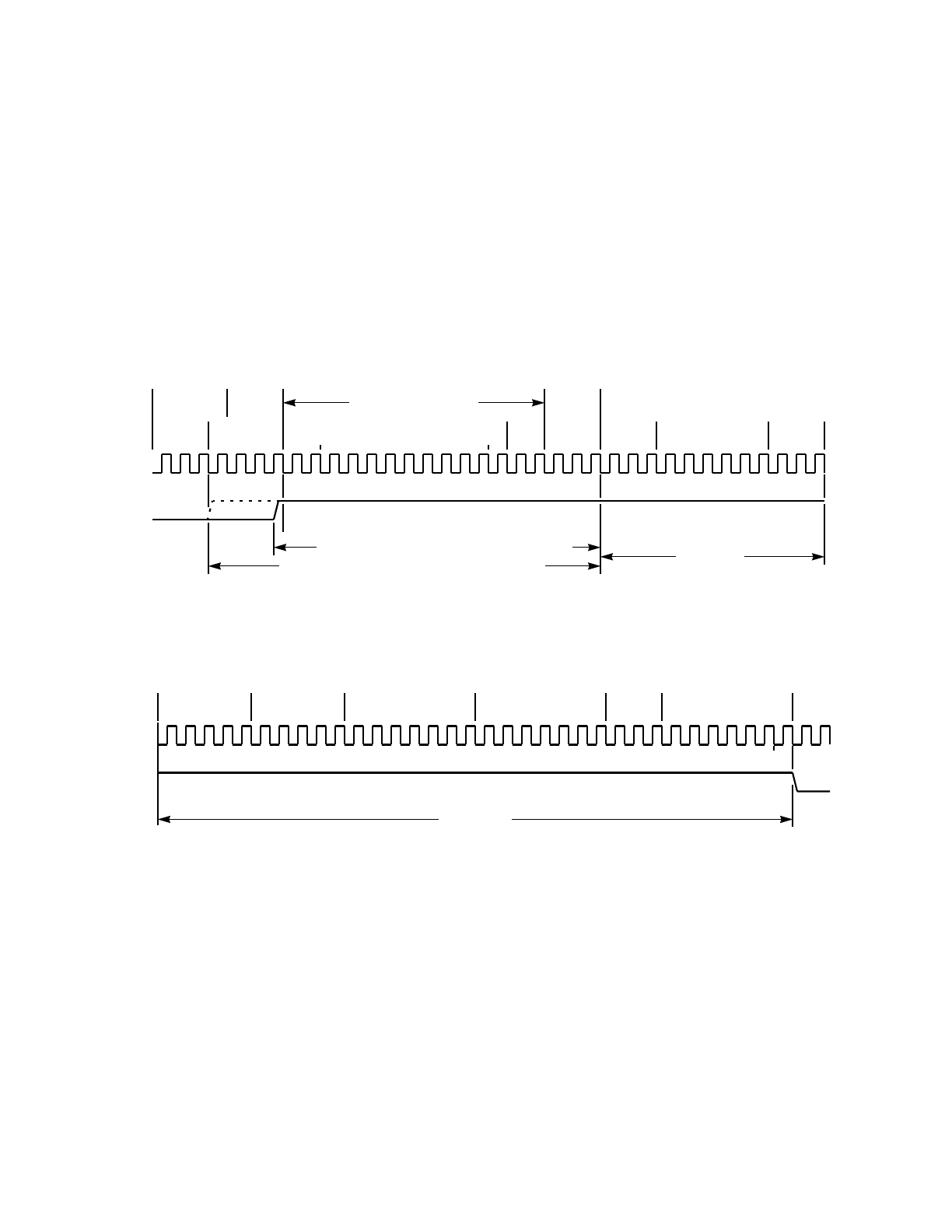
M68HC11 MAIN TIMER AND REAL-TIME INTERRUPT MOTOROLA
REFERENCE MANUAL 10-23
The response time in Figure 10-7 is slightly longer than it would be for a normal pro-
gram because of the pseudo-vector mechanism in the EVB board. The JMP instruc-
tion at [3] is not shown in Example 10–2 because it is actually constructed by program
instructions during the initialization portion of this example program. This indirect vec-
toring is done in the EVB board because the vectors are located in the monitor
EPROM and are not accessible to an EVB user. To allow use of the interrupts in an
EVB, the vectors were purposely pointed at specific RAM locations called pseudo-vec-
tors. A JMP instruction would be stored in these RAM locations, which points to the
start of the interrupt service routine. In a normal application, the starting address of the
interrupt service routine would be hard coded into the vector locations at the top of
memory. When an interrupt occurs, the user would vector directly to the service routine
rather than having to execute the extra JMP instruction.
(a) Leading Edge Latency
(b) Process First Edge, Earliest Opportunity for Second Edge
Figure 10-7 Timing Analysis for Example 10–2
The BNE NO1ST2 instruction at [5] will not branch during processing of the leading
edge of the pulse being measured. Execution continues with the LDD instruction in
Figure 10-7(b). The BCLR; BSET sequence at [6] is not as fast as a simple LDAA #,
STAA TCTL2, but the longer sequence was chosen because it does not disturb the
other bits in the register.
BEST CASE MINIMUM RESPONSE (17 CYCLES)
E
IC1
PIN
LDX
#REGBAS
INTERRUPT RESPONSE
[1]
[2]
[4] [5]
WORST CASE MINIMUM RESPONSE (21 CYCLES)
BEQ
WAITL2 LDAA
IC1DUN
LDAA
IC1DUN BEQ
WAITL2
VECT
PC
LHLHLHBACC
YYXX
EVB
PSEUDO
VECTOR
JMP
SV2IC1 INC IC1MOD BNE
NO1ST2
[3]
(12 CYCLES)
(34 CYCLES)
E
IC1
PIN
BRA
OU2IC1
BCLR TCTL2,X $30STD FRSTE
[6]
[7]
[8]
[9]
LDD TIC1,X BSET TCTL2,X $20 BCLR TFLG1,X $FB

MOTOROLA MAIN TIMER AND REAL-TIME INTERRUPT M68HC11
10-24 REFERENCE MANUAL
The earliest place the second edge could occur and be properly handled is during the
cycle after the status flag clear instruction [7], which occurs before returning from the
interrupt service routine after processing the leading edge of the pulse. If the second
edge came before this time, it would still be captured, but the IC1F flag would be
cleared by the clearing instruction intended to clear the flag from the first edge. The
minimum pulse width that can be measured by this program would be the time from
[1] or [2] through [7]. This time is a total of 63 to 67 cycles or about 34 µs.
This timing analysis is based on this specific example running by itself in the EVB
board and is not intended to show the smallest pulse that can be measured. Since no
other tasks are being performed in this example, the interrupt latency is somewhat
shorter than it would be in a realistic system. In a normal system, the user would not
have to work through the EVB’s pseudo-vector mechanism and would save three cy-
cles of latency time (because of the JMP in the pseudo-vector locations). Conversely,
in a real system, the user could get this interrupt just as a multiply instruction had start-
ed; thus, there could be a wait of up to 10 cycles (MUL takes 10 cycles) for that instruc-
tion to finish before servicing the input-capture interrupt. Worse yet, the user may have
just started servicing another interrupt source when the edge was recognized; thus,
the input capture would have to wait for that interrupt service routine to be completed
before it could be serviced. A much more detailed discussion of interrupts is presented
in SECTION 5 RESETS AND INTERRUPTS. The shortest pulse the user would be
able to measure in a realistic system will be a few hundred cycles rather than the few
dozen cycles shown in this isolated example.
This timing analysis is based on a detailed knowledge of timer logic and instruction tim-
ing. Instruction timing tells which cycle within the instruction actually reads or writes a
register. Instruction details can be found in APPENDIX A INSTRUCTION SET DE-
TAILS. Detailed information concerning timer captures is given in 10.5 Timing Details
For The Main Timer System. Detailed operation of the interrupt mechanism is pre-
sented in SECTION 5 RESETS AND INTERRUPTS.
10.3.4 Measuring Very Short Time Periods
Since the MC68HC11A8 has three input-capture functions, it is theoretically possible
to measure pulse widths as short as one timer count by connecting the signal to two
input-capture pins. One input capture is configured to detect the leading edge of the
pulse; whereas, the other is configured to detect the trailing edge. Although this func-
tion is possible, it is not commonly used.
10.3.5 Measuring Long Time Periods with Input Capture and Overflow
There are at least two ways to measure time periods that are longer than the range of
the 16-bit free-running timer. The following paragraphs discuss an example based on
input capture and counting timer overflows, which is accurate to ±1 timer count (500
ns in this case). If the user were measuring times in the seconds range to a resolution
of ±100 ms, a software approach might be easier than the input-capture/overflow
method. In the software approach, the user sets up a real-time loop structure where
the main program is executed once each tenth of a second. Other real-time periods
could be used, but a tenth of a second is easier. The user starts a software counter

M68HC11 MAIN TIMER AND REAL-TIME INTERRUPT MOTOROLA
REFERENCE MANUAL 10-25
when the signal first changes, increments the count once each time through the main
loop, and stops the count at the end of a period. This method is very simple and yields
an accuracy of ± 100 ms, which is quite reasonable for many applications.
To measure a time greater than the range of the 16-bit main timer counter with an input
capture, timer overflows must be considered. A program is presented that extends the
range of the timer to 24 bits by keeping track of overflows in an 8-bit software counter.
By increasing the size of this software counter, the user could measure even longer
periods. At 2-MHz bus speed and a divide by one prescale factor, 24 bits allow the
user to measure periods up to about 8.38 s.
The most difficult part of this procedure is deciding whether or not to count an overflow
when a capture occurs very close to a timer overflow. Given some assumptions, the
user can tell if the capture happened before or after the overflow by looking at the MSB
of the captured value. Once the user knows which happened first, the case can be
treated accordingly.
First, assume that all timer overflow conditions (TOF= 1) will be handled before the
MSB of the free-running counter becomes set again (that is, in less than half the time
between successive overflows). If TOF and ICxF are both set and the captured value
has a one in its MSB, then the user knows the capture occurred before the overflow.
Conversely, if TOF and ICxF are both set and the captured value is positive (MSB =
0), then the capture occurred after the overflow. Servicing an overflow interrupt takes
less than 15 ms, even in a busy system.
Second, assume that if a capture and an overflow happen in the vicinity of each other,
the input capture will be serviced before the overflow. Vicinity means so close together
that both are pending when the user reaches the input-capture service routine. The
input-capture routine checks for a close overflow; therefore, if an overflow occurred
just after the leading edge or just before a trailing edge of a measurement period, it
can be included correctly. This assumption is needed to avoid the possibility of missing
an overflow that should have been counted or to avoid counting one that occurred just
outside the period being measured. Again, this condition is easy to service because
timer overflow is a lower priority interrupt than input captures. The only way an over-
flow can be serviced before an input capture that occurred in the vicinity is if the over-
flow happened enough before the input capture for the stacking and vector selection
to be completed before the capture is detected. Such a case, which is no different from
having the overflow occur long before the capture, is treated correctly without taking
any special action.
Example 10–3 uses input capture and counts overflows in an 8-bit software counter to
allow measurement of periods between about 70 and 16,777,215 cycles (35 RSto
8.38 s). The program runs on an EVB board and displays results on the EVB terminal
display. The important parts of the program are shown in Figure 10-8; see 10.6 List-
ing of Timer Examples for a complete listing. Example 10–3 was specifically struc-
tured to allow easy expansion to other functions. For example, two more period
measurement functions can be added by adding a few instructions to the overflow ser-
vice routine and basically duplicating the IC1 service routine for IC2 and IC3. The fol-
lowing lines of code are from Example 10–3:

MOTOROLA MAIN TIMER AND REAL-TIME INTERRUPT M68HC11
10-26 REFERENCE MANUAL
c191 a6 25 [4] LDAA TFLG2,X Check for TOF in MSB
c193 2a 23 [3] BPL OU3IC1 If no overflow, you’re done
c195 7a d0 07 [6] DEC OVCNT1 This TOF shouldn’t count
* decrement OVCNT1 to -1, TOF svc routine will inc to 0
This example demonstrates the idea of indicating the TOF should not count rather
than directly clearing it to make it not count. Although the TOF is not needed for this
period measurement function, it may be needed for some other function that might be
in progress. Although the three input-capture functions and the five output-compare
functions are effectively independent of each other, they are all specifically related to
the single, 16-bit, free-running counter and thus share the overflow mechanism. The
capture and compare functions can independently monitor the overflow, but they
should not directly interfere with its operation.
*** initialization - (see full listing) ***
c114 ce 10 00 [3] PER24T LDX #REGBAS Point to register block
c117 86 10 [2] LDAA #%00010000 EDG1B:EDGIA - 0:1
c119 a7 21 [4] STAA TCTL2,X IC1 rising edges
c11b 86 ff [2] LDAA #$FF
c11d b7 d0 06 [4] STAA IC1MOD FF-IC1 off; 0-1st edge; 1-last
c120 7f d0 05 [6] CLR IC1DUN Signal period not done
c123 1d 23 fb [7] BCLR TFLG1,X $FB clear IC1F (if any)
c126 1d 25 7f [7] BCLR TFLG2,X $7F clear TOF (if any)
c129 1c 22 04 [7] BSET TMSK1,X $04 enable IC1 interrupts
c12c 1c 24 80 [7] BSET TMSK2,X $80 enable TOF interrupts
c12f 0e [2] CLI Enable Interrupts
c130 b6 d0 05 [4] WAITL3 LDAA IC1DUN Sets after period done
c133 27 fb [3] BEQ WAITL3 Loop till period has been timed
c135 0f [2] SEI Done, disable interrupts
** display results - (see full listing)
***
* SV3TOF - Timer Overflow service routine
*
* Called whenever any timer overflow is detected.
* If the IC1 period measurement is in progress
* (IC1MOD positive) then the overflow counter
* (upper 8-bits of period) is incremented.
***
c171 7d d0 06 [6] SV3TOF TST IC1MOD 0 or 1, IC1 active; count TOFs
c174 2b 03 [3] BMI OU3TOF if neg, IC1 not active
c176 7c d0 07 [6] INC OVCNT1 increment IC1 overflow count
c179 86 80 [2] OU3TOF LDAA #$80
c17b b7 10 25 [4] STAA REGBAS+TFLG2Clear overflow flag
c17e 3b [12] RTI ** Return from TOF service **
Figure 10-8 Measuring Long Periods with Input Capture and TOF (Sheet 1 of 2)
***

M68HC11 MAIN TIMER AND REAL-TIME INTERRUPT MOTOROLA
REFERENCE MANUAL 10-27
* SV3IC1 - Input Capture 1 service routine
*
* Called at start and end of a period being measured
***
c17f ce 10 00 [3] SV3IC1 LDX #REGBAS point at top of register block
c182 7c d0 06 [6] INC IC1MOD $FF->O at 1st edge; 0->1 at 2nd
c185 26 13 [3] BNE NO1ST3 if not 0, this is second edge
* Process first edge of period
c187 7f d0 07 [6] CLR OVCNT1 Zero the overflow count
c18a ec 10 [5] LDD TIC1,X Read time of first edge
c18c fd d0 08 [5] STD RES1 Save till next capture
c18f 2b 27 [3] BMI OU3IC1 If IC was before any overflow
c191 a6 25 [4] LDAA TFLG2,X Check for TOF in MSB
c193 2a 23 [3] BPL OU3IC1 If no overflow, you’re done
c195 7a d0 07 [6] DEC OVCNT1 This TOF shouldn’t count
* decrement OVCNT1 to -1, TOF svc routine will inc to 0
c198 20 1e [3] BRA OU3IC1 Done processing first edge
* Process second edge of period
c19a ec 10 [5] NO1ST3 LDD TIC1,X Get time of second edge
c19c 2b 07 13] BMI ARNOV1 If MSB-1, skip TOF check
c19e 6d 25 [6] TST TFLG2,X Check for overflow
c1a0 2a 03 [3] BPL ARNOV1 If no TOF, skip increment
c1a2 7c d0 07 [6] INC OVCNT1 TOF was before edge so count it
c1a5 b3 d0 08 [6] ARNOV1 SUBD RES1 (Time of last) - (time of 1st)
c1a8 fd d0 08 [5] STD RES1 Update result
c1ab 24 03 [3] BCC RES1OK Check for borrow
c1ad 7a d0 07 [6] DEC OVCNT1 If borrow, fix overflow count
c1b0 1d 21 30 [7] RES1OK BCLR TCTL2,X $30 Disable IC1
c1b3 86 01 [2] LDAA #1
c1b5 b7 d0 05 [4] STAA lC1DUN Signal period measured
c1b8 1d 23 fb [7] OU3IC1 BCLR TFLG1,X $FB Clear IC1F
c1bb 3b [12] RTI ** Return from IC1 service
Figure 10-8 Measuring Long Periods with Input Capture and TOF (Sheet 2 of 2)
10.3.6 Establishing a Relationship between Software and an Event
In common MCU applications, a software program must generate various output con-
trol signals as a result of various input signals or events. A software program monitors
the input signals and produces output signals as needed. Sometimes it is important for
the output signals to be in some strict timing relationship to an input signal. A problem,
which is called latency, arises when software requires some time to notice and re-
spond to an input event. In many MCU systems, this latency determines the worst-
case uncertainty in the ability of software to know exactly when an event occurred and
the accuracy of the timing relationship between the event and a resulting output signal.
In the MC68HC11A8, the timer system allows much more accurate control of the re-
lationship between events and resulting output signals.
The critical input signal will drive one of the input-capture pins of the MCU. When an
event (edge) occurs on this pin, the input-capture function automatically latches the
current value of the free-running timer counter. Even though software takes a variable

MOTOROLA MAIN TIMER AND REAL-TIME INTERRUPT M68HC11
10-28 REFERENCE MANUAL
amount of time to respond to the event, the time at which it took place was latched (re-
corded), thus eliminating uncertainty due to software latency. Now software can read
the timer counter to determine the present timing relationship between the program
and when the event occurred. Better yet, an output-compare function can be set up to
produce the desired output signal action at another specific value of the timer counter
(i.e., at another specific time relative to the input event). Since both the input event and
the output action are referenced to the same timer counter, the resolution of the
counter determines the worst-case uncertainty in the timing relationship. Although
software latency still determines the minimum controllable delay between the input
event and the output action, it no longer influences the accuracy of the timing relation-
ship.
10.3.7 Other Uses for Input-Capture Pins
At any time, software can read the logic levels on the pins used for input-capture func-
tions (even if the input-capture function is enabled). These three pins may also be
used as flexible interrupt input pins when the timer input-capture functions are not
needed. Each of these pins can be used as a separate edge-triggered interrupt with
its own interrupt vector. The significant edge(s) can be individually selected by the
control bits in the TCTL2 register. An important advantage of these interrupt pins over
the IRQ pin is that these interrupts can be enabled/disabled with the local interrupt en-
able bits (ICxI) in the TMSK1 register. Another advantage of these pins is that there is
a readable status indicator (ICxF) so software can tell if an interrupt request is pending
from these sources. Software can also choose to clear any pending interrupt from one
of these sources before enabling it. As with all maskable interrupt sources, interrupts
can be disabled from these pins by setting the I bit in the CCR in the CPU.
10.4 Output-Compare Functions
Rather than being specifically configured to perform a single function, such as vari-
able-frequency square-wave generation, the output-compare functions in the
MC68HC11A8 are configured and controlled by software-accessible control registers
and bits so they can perform a wide variety of tasks. Although some software overhead
exists for some common timing functions, such as pulse-width modulation (PWM) sig-
nals, these software-controlled output-compare functions are easily adaptable to a
much wider range of applications than dedicated timer functions would be.
There are five output-compare functions in the MC68HC11A8. Each output compare
has a 16-bit compare register and a dedicated 16-bit comparator. The comparator
checks the free-running timer value against the 16-bit compare register during every
timer count. When a match is detected, a status flag is set (OCxF), an interrupt is op-
tionally generated, and timer output pins are automatically changed according to soft-
ware-accessible control bits. Since each of the five interrupts is separately maskable
with a local interrupt enable control bit and since each has its own interrupt vector,
there is no need to perform any software polling to determine the cause of an interrupt.
Four of the output compares operate much like the output compares on the M6801
Family of MCUs except that the M68HC11 has more output-compare channels and
has slightly more control over the timer output pins. The fifth output compare on the

M68HC11 MAIN TIMER AND REAL-TIME INTERRUPT MOTOROLA
REFERENCE MANUAL 10-29
MC68HC11A8 (OC1) can control any combination of the five timer output pins even if
another output compare is already controlling the pin(s). The value and implications of
this feature will be explained in greater detail.
For OC[5:2], a pair of control bits in the timer control register 1 (TCTL1) control the au-
tomatic action that will occur at the respective timer output pin when an output com-
pare happens (16-bit OCx register matches the free-running timer). The control bit
pairs (OMx, OLx, x = 2, 3, 4, or 5) are encoded to allow the four following possibilities:
1) timer output compare causes no pin change; 2) toggle pin on each successful com-
pare; 3) force pin to zero on a successful compare; and 4) force pin to one on a suc-
cessful compare. Each of the output compares (OC[5:2]) is associated with a separate
port A pin, and the automatic pin actions for each output compare are independently
controlled.
For OC1, the automatic pin actions are controlled by the OC1 mask (OC1M) and OC1
data (OC1D) registers. The OC1M register specifies which port A pins are to be affect-
ed by OC1. The OC1D register specifies the data to be sent to the affected port A
pin(s) when there is a successful OC1 match. If OC1 and another output compare are
both controlling the same pin and if both attempt to change the pin simultaneously,
OC1 will have priority.
Output pins for the five output-compare functions can be used as general-purpose out-
put pins having nothing to do with the timer system or as timer outputs directly con-
trolled by the timer system. When one of these pins is configured for timer use, it
cannot be written directly from software as a general-purpose port A output line. If the
user needs to change a timer output pin without waiting for an actual output compare,
the force output-compare function can be used. This function may be used to initialize
the state of timer outputs or to force an output change before it was scheduled to occur
by the associated output-compare register. Another way to change the state of a timer
output pin is to temporarily disengage the timer by changing the timer control registers.
This method requires a more detailed understanding of the actual port A pin logic. De-
tailed schematics of the port A output pins are shown and explained in SECTION 7
PARALLEL INPUT/OUTPUT.
The 16-bit output-compare register for each output-compare function can be read or
written by software as a pair of 8-bit registers. The TOCx registers are forced to $FFFF
during reset.
A write to the high-order byte of an output-compare register pair inhibits the output-
compare function for one bus cycle. This inhibit prevents erroneous comparisons us-
ing a 16-bit value whose high-order half was just written and whose low-order half still
contains data from the previous output-compare value. Consider the case where an
output-compare register is $FF0F and the user tries to write it to $00FF as the free-
running timer is counting through the value $000F. Without the one-cycle inhibit after
writing to the upper half of the output-compare register, an erroneous compare could
occur at $000F. As long as the user utilizes a double-byte write instruction, such as
store D (STD), to update output-compare registers, this one-cycle inhibit mechanism
will assure that no unintentional compares will result after the write of the high-order
half but before the write of the low-order half.

MOTOROLA MAIN TIMER AND REAL-TIME INTERRUPT M68HC11
10-30 REFERENCE MANUAL
As long as an output-compare function is configured to change a pin state or to gen-
erate an interrupt, the action occurs every time the timer-count value matches the
compare register (not just the first time a match occurs). To generate a single interrupt
after some delay, read the TCNT register, add a value corresponding to the desired
delay, write that value to the output-compare register, and write the appropriate con-
trols to enable the interrupt. When the interrupt occurs, write the appropriate controls
to disable the interrupt, or another interrupt will occur as soon as the free-running timer
rolls around to the output-compare register value again.
The following registers and paragraphs explain the output-compare status flags and
the local interrupt enable control bits for the output-compare functions.
OCxI, OCxF — Output Compare Interrupt Enables and Output Compare Flags (x= 1, 2,
3, 4, or 5)
The OCxF status bit is automatically set to one each time the corresponding output-
compare register matches the free-running timer. This status bit is cleared by writing
to the TFLG1 register with a one in the corresponding data bit position. The OCxI con-
trol bit allows the user to configure each output-compare function for polled or inter-
rupt-driven operation but does not affect the setting or clearing of the corresponding
OCxF bit. When OCxl is zero, the corresponding output-compare interrupt is inhibited,
and the output compare is operating in a polled mode. In this mode, the OCxF bit must
be polled (read) by user software to determine when a match has been detected.
Bit 7 654321Bit 0
$1016 Bit 15 ——————Bit 8 TOC1
$1017 Bit 7 ——————Bit 0
$1018 Bit 15 ——————Bit 8 TOC2
$1019 Bit 7 ——————Bit 0
$101B Bit 7 ——————Bit 0
$101C Bit 15 ——————Bit 8 TOC4
$101D Bit 7 ——————Bit 0
$101E Bit 15 ——————Bit 8 TOC5
$101F Bit 7 ——————Bit 0
TMSK1 — Timer Interrupt Mask Register 1 $1022
BIT 7 654321BIT 0
OC1I OC2I OC3I OC4I OC5I IC1I IC2I IC3I
RESET: 00000000
TFLG1 — Timer Interrupt Flag Register 1 $1023
BIT 7 654321BIT 0
OC1F OC2F OC3F OC4F OC5F IC1F IC2F IC3F
RESET: 00000000

M68HC11 MAIN TIMER AND REAL-TIME INTERRUPT MOTOROLA
REFERENCE MANUAL 10-31
When the OCxl control bit is one, a hardware interrupt request is generated whenever
the corresponding OCxF bit is set to one. Before leaving the interrupt service routine,
software must clear the OCxF bit by writing to the TFLG1 register (see 10.2.4 Tips for
Clearing Timer Flags).
Example 10–4 is a very simple program that uses an output compare to control a soft-
ware time delay. For simplicity, this example uses polled mode and does not cause
any automatic pin changes as the result of the output compare. The program gener-
ates a 10-ms delay like the user might utilize to time an EEPROM program or erase
operation; however, instead of actually programming EEPROM, it will just produce a
pulse on an output port pin so the results can be studied on an oscilloscope. Output-
compare functions can also cause automatic pin changes and generate interrupt re-
quests (see Examples 10–5 and 10–6). A partial listing of the program for Example
10–4 is shown in Figure 10-9.
c1bc ce 10 00 [3] INZA LDX #REGBAS Point to register block
c1bf 86 80 [2] LDAA #$80
c1c1 a7 23 [4] STAA TFLG1,X Clear any pending OC1F flag
c1c3 6f 04 [6] CLR PORTB,X Initialize port B to zeros
c1c5 86 01 [2] TOP4A LDAA #1 Top of Ex10-4a
c1c7 a7 04 [4] STAA PORTB,X Set LSB of port B
* This is where the 10mS delay part actually starts
*
c1c9 ec 0e [5] LDD TCNT,X Get current timer count
c1cb c3 4e 20 [4] ADDD #20000 What will count be in 10mS?
c1ce ed 16 [5] STD TOC1,X Set OC1 to trigger then
c1d0 1f 23 80 fc[7] LP1 BRCLR TFLG1,X $80 LP1 Loop here till OC1F=1
*Delay is actually done here; rest is just support
c1d4 1d 23 7f [7] BCLR TFLG1,X $7F Clear OC1F
c1d7 6f 04 [6] CLR PORTB,X Clear PB0 pin
c1d9 18 ce 16 4e[4] LDY #5710 5710*(7~/loop) = about 20ms
c1dd 18 09 [4] DLP1 DEY Top of software delay loop
c1df 26 fc [3] BNE DLP1 Loop ’till Y is zero
c1e1 20 e2 [3] BRA TOP4A Repeat continuously for O-scope
Figure 10-9 Simple Output-Compare Example
This example is only intended to show the most basic use of an output-compare func-
tion. It is not intended to be an especially efficient way to delay a fixed period of time.
The following three instructions are a simpler way to delay if no other tasks are to be
performed during the delay:
c1d9 18 ce 16 4e[4] LDY #5710 5710*(7~/loop)= about 2Oms
c1dd 18 09 [4] DLP1 DEY Top of software delay loop
c1df 26 fc [3] BNE DLP1 Loop ’till Y is zero
By contrast, an output compare in interrupt-driven mode has the advantage of allowing
MOTOROLA MAIN TIMER AND REAL-TIME INTERRUPT M68HC11
10-32 REFERENCE MANUAL
the user to perform other tasks while waiting for the delay.
10.4.1 Normal I/O Pin Control Using OC[5:2]
The user can independently program the automatic pin actions to occur for each out-
put-compare function. For OC[5:2], a pair of control bits (OMx, OLx) in TCTL1 are used
to control the automatic pin actions.
OMx, OLx — Output Compare Pin Control (x = 1, 2, 3, 4, or 5)
This pair of bits determines the automatic actions that occur on the port A timer output
pin when there is a successful output compare. Each OC[5:2] function corresponds to
a specific pin of port A. Each pair of bits controls the action for the corresponding out-
put-compare function. These bit pairs are encoded as shown in the following table:
Example 10–5 uses OC2 to generate a square wave at the PA6/OC2 pin. The program
runs on an EVB board, and the results are monitored with an oscilloscope. Before run-
ning this program, manually set the half-cycle delay time (as a number of cycles) in the
double-byte location HDLY ($D000,D001). For example, if $01,00 is stored at
$D000,D001, a square wave with a period of 256 µs would be generated (half period
= 256 cycles x 500 ns/cyc). Figure 10-10 shows the program for Example 10–5.
The initialization of the pseudo-vector at the top of Example 10–5 is done for the EVB
board and would not be a normal part of a practical application. The three cycles need-
ed for the extra JMP instruction are shown at [3] in Figure 10-11.
TCTL1 — Timer Control Register 1 $1020
BIT 7 654321BIT 0
OM2 OL2 OM3 OL3 OM4 OL4 OM5 OL5
RESET: 00000000
OMx OLx Configuration
0 0 OCx does not affect pin (OC1 still may)
0 1 Toggle OCx pin on successful compare
1 0 Clear OCx pin on successful compare
1 1 Set OCx pin on successful compare

M68HC11 MAIN TIMER AND REAL-TIME INTERRUPT MOTOROLA
REFERENCE MANUAL 10-33
c1e3 8e 00 47 [3] TOP5 LDS #$0047 Top of User’s Stack area on EVB
c1e6 86 7e [2] LDAA #$7E Jump (extended) Opcode
c1e8 97 dc [3] STAA PVOC2 Pseudo Vector see manual text
c1ea ce c1 fd [3] LDX #SV5OC2 Address of OC2 service routine
c1ed df dd [4] STX PVOC2+1 Finish jump instruc to TOF svc
c1ef ce 10 00 [3] LDX #REGBAS Point to register block
c1f2 86 40 [2] LDAA #%01000000 OM2:OL2 = 0:1
c1f4 a7 20 [4] STAA TCTL1,X Set OC2 for toggle, on compare
c1f6 a7 23 [4] STAA TFLG1,X Clear any pending,OC2F
c1f8 a7 22 [4] STAA TMSK1,X Enable OC2 interrupts
c1fa 0e [2] CLI Enable Interrupts
c1fb 20 fe [3] BRA * Interrupt driven; sit here
***
* SV5OC2 - Output Compare 2 service routine
*
* Called at each OC2 interrupt.
***
c1fd fc d0 00 [5] SV5OC2 LDD HDLY Get delay time for 1/2 cycle
c200 e3 18 [6] ADDD TOC2,X Add to last compare value
c202 ed 18 [5] STD TOC2,X Update OC2 (schedule next edge)
c204 1d 23 bf [7] BCLR TFLG1,X $BF Clear OC2F
c207 3b [12] RTI ** Return from OC2 service **
Figure 10-10 Generating a Square Wave with Output Compare
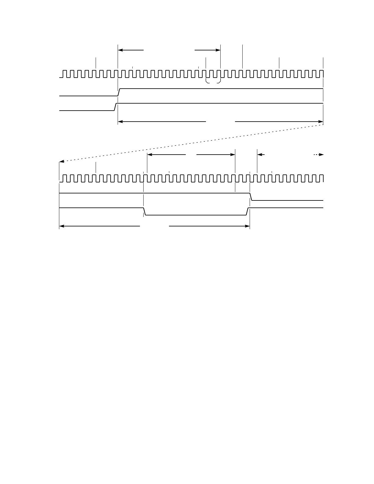
MOTOROLA MAIN TIMER AND REAL-TIME INTERRUPT M68HC11
10-34 REFERENCE MANUAL
Figure 10-11 Timing Analysis for Example 10–5
Figure 10-11 shows a detailed timing analysis for Example 10–5. This degree of detail
is not normally needed, but this analysis shows exactly what occurs during an interrupt
driven output compare. The timer count has a fixed relationship to real time; whereas,
software can be aligned to the timer count in any of several ways. It is generally not
known (nor does it need to be) which of these several possible relationships is correct.
Although software latencies do not affect the accuracy with which output edges are
placed, these latencies do determine the shortest possible delay between successive
output edges. In this isolated example, the software latencies are quite short, but in a
practical application, latencies from other interrupt sources must be considered.
This timing analysis shows the case where the half-period delay (HDLY) is 54 cycles,
and the OC2F was set just before the BRA * finished [1]. This analysis represents the
fastest response to the OC2F bit. The flag is actually set [1] just before the pin state
changes. The exact timing of the flag and pin changes is discussed in detail in 10.5
Timing Details For The Main Timer System. The period can be set as short as 52
cycles (the total time needed to service each interrupt from [1] to [8]).
This example is intended to show a way to produce a simple square wave and is not
intended to be the most efficient way to perform this task.
(28 CYCLES)
E
INTERRUPT RESPONSE
[1] [4] [5]
VECT
PC
LHLHLHBACC
YYXX
EVB
PSEUDO
VECTOR
JMP
SV5OC2 LDD HDLY
[3]
OC2
PIN
[2]
BRA∗ADDD TOC2,X
OC2F
(26 CYCLES)
E
INTERRUPT RESPONSE
[7] [9]
PC
LHLHLHB
YYXX
[8]
OC2
PIN
BRA∗
STD TOC2,X BCLR TFLG1,X $BF
OC2F
PC
LHL HL HBACC
YYXX
RTI
[6]

M68HC11 MAIN TIMER AND REAL-TIME INTERRUPT MOTOROLA
REFERENCE MANUAL 10-35
10.4.2 Advanced I/O Pin Control Using OC1
One of the five output-compare functions (OC1) in the MC68HC11A8 has special timer
output pin controls that were not present on any previous Motorola MCUs. These new
controls allow this output-compare function to simultaneously control the states of up
to five output pins. This output compare can also be configured to control a pin or pins
that are also being controlled by one of the other four output-compare functions.
OC1 uses the OC1M and the OC1D to control the automatic timer output pin actions
occurring as a result of a match between the OC1 register and the free-running timer.
Each of the five MSBs of these registers corresponds bit-for-bit with a port A output
pin. The three remaining low-order bits of these registers are not used and always read
as zeros. For each port A output pin to be affected by OC1, the user would set the cor-
responding bit of OC1M. When a successful OC1 compare occurs, each port A pin to
be affected (indicated by the corresponding bit of OC1M set) will assume the value of
the corresponding bit of OC1D. Values of bits in OC1D corresponding to zeros in the
OC1M register are don’t cares. Usually, the user only has to write to the OC1M register
once to establish which pins will be controlled by OC1. The relationship between reg-
ister bits and port A pins is provided in the reference below the following registers:
OC1 can only affect the PA7 pin if the pin is configured as an output as opposed to its
default configuration as an input. To configure PA7 as an output, the data direction
control bit for port A bit 7 (DDRA7) in the pulse accumulator control register (PACTL)
must be set to one.
10.4.2.1 One Output Compare Controlling up to Five Pins
The special pin control mechanisms on OC1 allow it to simultaneously control as many
as five timer output pins. (Software can be used to allow any single output compare to
control multiple outputs, but software latency will affect the resolution and the ability to
repeat timed actions accurately.) The OC1 mechanism allows pins to be controlled
with a timing accuracy equal to one count of the timer counter.
The ability to control multiple outputs with a single output-compare channel is espe-
cially useful where the outputs are all associated with a single external device — for
example, the signals driving a stepper motor. In such a case, it is always possible to
know the required state for all of the outputs whenever any one is going to change. On
OC1M — Output Compare 1 Mask $100C
BIT 7 654321BIT 0
OC1M7 OC1M6 OC1M5 OC1M4 OC1M3 0 0 0
RESET: 00000000
OC1D — Output Compare 1 Data $100D
BIT 7 6 5 4 3 2 1 BIT 0
OC1D7 OC1D6 OC1D5 OC1D4 OC1D3 0 0 0
RESET: 0 0 0 0 0 0 0 0
REFERENCES: PA7/PA1 PA6/OC2 PA5/OC3 PA4/OC4 PA3/OC5 PA2/IC1 PA1/IC2 PA0/IC3

MOTOROLA MAIN TIMER AND REAL-TIME INTERRUPT M68HC11
10-36 REFERENCE MANUAL
the other hand, if the outputs control unrelated devices, it might be more practical to
use separate output-compare channels for each output.
A side benefit to using OC1 to control several timer outputs is that the other output-
compare functions associated with these pins become available for general-purpose
software timing functions that do not directly control pins.
10.4.2.2 Two Output Compares Controlling One Pin
OC1 can also be used in conjunction with one or more other output compares to
achieve even more timing flexibility. OC1 can control a timer output even when one of
the other output compares is already controlling the same pin, which allows the pro-
grammer to schedule two succeeding edges of each output signal at a time. This ca-
pability reduces software overhead because only one of the two output compares
needs to generate an interrupt. Pulses as short as one E cycle, which are accurately
positioned with one-cycle resolution (500-ns resolution), can be generated.
Example 10–6 uses OC1, OC2, and OC3 together to produce two PWM outputs. This
particular program can produce active-high PWM signals with a minimum period of
200 cycles (100 µs or 10 kHz) and a duty cycle of 0 to 100 percent. Actually, the pro-
gram only produces duty cycles of 50 to 100 percent. When a smaller duty cycle is
specified, it is automatically changed to 100 percent minus the specified duty cycle,
and the polarity of the output is switched. (A 30-percent active-high duty cycle is the
same as a 70-percent active-low duty cycle.) Figure 10-12 shows the important parts
of the program for Example 10–6.
Before running this example program on the EVB board, the period and duty cycle are
established manually with memory modify commands. Period is set indirectly by set-
ting the location PWMP1P at $D002. This value is one percent of the period (in cycles);
thus, a value of $02 sets the period to 200 cycles. When the program starts, this value
is multiplied by 100 and stored to location PWMPER. Program latencies are such that
a period of 100 cycles (PWMP1P = $01) is too short, and the program will not operate
correctly. Duty cycles are stored as percentages at locations PWMDC1 and PWMDC2
($D003 and $D004, respectively; $64 = 100 percent).

M68HC11 MAIN TIMER AND REAL-TIME INTERRUPT MOTOROLA
REFERENCE MANUAL 10-37
*** initialization - (see full listing) ***
c217 86 50 [2] LDAA #%0l010000 OMx:OLx = 0:1 for toggle
c219 a7 20 [4] STAA TCTL1,X OC2 and OC3 for toggle
c21b 86 70 [2] LDAA #%01110000 OClM6,5, & 4 - 1
c21d a7 0c [4] STAA OCIM,X Control OC2/PA6, OC3/PA5, & PA4
c21f 5f [2] CLRB Build OC1D initial value in B
c220 b6 d0 03 [4] LDAA PWMDC1 Check for OC2 duty > or = 50%
c223 81 32 [2] CMPA #50 If <50% OC1 drives low...
c225 23 02 [3] BLS ARNZ61 and OC2 toggles high.
c227 cb 40 [2] ADDB #%01000000 Else OC1 driv high/OC2 tog low
c229 b6 d0 04 [4] ARNZ61 LDAA PWMDC2 Check for OC3 duty > or = 50%
c22c 81 32 [2] CMPA #50 If <50% OC1 drives low...
c22e 23 02 [3] BLS ARNZ62 and OC3 toggles high.
c230 cb 20 [2] ADDB #%00100000 Else OC1 driv high/OC3 tog low
c232 e7 0d [4] ARNZ62 STAB OC1D,X Store starting value for OC1D
* Calculate period & duty cycle as cycle count offsets
c234 b6 d0 02 [4] LDAA PWMP1P 1% of period
c237 c6 64 [2] LDAB #100
c239 3d [10] MUL 100 * PWMP1P = PWMPER
c23a fd d0 1f [5] STD PWMPER Store period
c23d ed 16 [5] STD TOC1,X Start with TCNT = PWMPER
c23f b6 d0 03 [4] LDAA PWMDC1 Calculate offset for OC2
c242 8d 12 [6] BSR CALOFF Adj duty and calc offset
c244 ed 18 [5] STD TOC2,X Schedule first OC2 toggle
c246 b6 d0 04 [4] LDAA PWMDC2 Calculate offset for OC3
c249 0d 0b [6] BSR CALOFF Adj duty and calc offset
c24b ed 1a [5] STD TOC3,X Schedule first OC3 toggle
c24d 86 80 [2] LDAA #$80 Finish initialization
c24f a7 23 [4] STAA TFLG1,X Clear any old OC1 flag
c251 a7 22 [4] STAA TMSK1,X Enable OC1 interrupt
c253 0e [2] CLI
c254 20 fe [3] BRA * PWMs driven by OC1 interrupts
***
* SV6OC1 - Output Compare 1 service routine
***
c269 ce 10 00 [3] SV6OCI LDX #REGBAS Point to register block
c26c a6 0d [4] LDAA OC1D,X Change state of PA4 at next OC1
c26e 88 10 [2] EORA #%00010000 Inverts OClD4 (PA4 pin control)
c270 a7 0d [4] STAA OC1D,X Update OC1 automatic pattern
c272 0c 18 [5] LDD TOC2,x Get last OC2 compare value
c274 f3 d0 1f [6] ADDD PWMPER Add count equiv to period
c277 ed 18 [5] STD TOC2,X Update OC2 (schedule next OC2)
c279 ec 1a [5] LDD TOC3,x Get last OC3 compare value
c27b f3 d0 1f [6] ADDD PWMPER Add count equiv to period
c27e ed 1a [5] STD TOC3,X Update OC3 (schedule next OC3)
c280 ec 16 [5] LDD TOC1,X Get last OC1 compare value
c282 f3 d0 1f [6] ADDD PWMPER Add count equiv to period
c285 ed 16 [5] STD TOC1,X Update OC1 (schedule next OCl)
c287 1d 23 7f [7] BCLR TFLG1,X $7F Clear OC1F
c28a 3b [12] RTI ** Return from OC1 service **
Figure 10-12 Producing Two PWM Outputs with OC1, OC2, and OC3
The larger upper portion of this program is executed only once to set up and to start
the PWM outputs. After this initial setup, the PWM signals are free running and are
controlled by OC1 interrupts only. When an OC1 interrupt occurs, a value equal to the
period is added to each of the output-compare registers (TOC1, TOC2, and TOC3).
When this OC1 service routine is enabled, the PWM outputs will have been forced to
their active level by the OC1 match that requested the interrupt. When this service rou-
tine is done, OC1 is set to start the next PWM period; OC2 and OC3 are set to termi-
nate the current PWM pulse. The PWM pulses, which are known to be at least 50

MOTOROLA MAIN TIMER AND REAL-TIME INTERRUPT M68HC11
10-38 REFERENCE MANUAL
percent of the period, control how quickly the OC1 service routine must finish (OC2
and OC3 must be scheduled in time to occur as early as 50 percent of the way to the
next PWM pulse start). The OC1 interrupt service takes almost 100 cycles, but OC2
and OC3 are updated somewhat before the end of the routine. Thus, the theoretical
minimum period is about 140 cycles (two times 70 cycles, where 70 cycles is the ap-
proximate latency time from an OC1 interrupt request to when OC2 and OC3 have
been updated). Because the example was set up so that period is specified by the
number of cycles in one percent of the period, a value of two makes period equal 200
cycles, which is acceptable; whereas, a value of one makes period equal 100 cycles,
which is too small.
This example is only one of many ways to generate PWM signals in the M68HC11.
Example 10–7 demonstrates an alternate way, which uses only one output compare.
The approach used in that example does not allow the duty cycle to be too close to 0
or 100 percent because there is a minimum latency requirement between any two suc-
cessive edges on the PWM output signal. In general, any approach will be subject to
some unique set of limitations. As with many engineering problems, there is no single
best solution; the user will have to select the best method based on all the application
requirements.
10.4.3 Forced Output Compares
The output-compare force mechanism provides a convenient way to change timer out-
put pin states without actually setting up and waiting for an output-compare match.
The force mechanism is useful to force an initial state at the start of a timing sequence
or to force an output compare earlier than it was scheduled. Consider the case where
the user has scheduled an output compare to occur at a certain time, but as the time
approaches, the user decides instead the compare should occur as soon as possible.
(This case is an actual situation that arises in spark timing control in some automotive
engine control applications.) In the older M6801 Family MCU, the user had to read the
timer counter, add a small value to it corresponding to a software delay, and write this
value to the output-compare register so that a compare match would occur at the next
E-clock cycle after the compare register update. With the force mechanism in the
M68HC11 Family, the user writes to the CFORC register to force any combination of
output-compare channels to trigger.
To use the output-compare force mechanism, the user would write to the CFORC reg-
ister with ones in the bit positions corresponding to the output-compare channels to be
forced. Writing a zero to a bit in the CFORC register has no effect on the correspond-
ing output-compare channel. At the next timer count after the write to CFORC, the
forced channels will trigger their programmed pin actions to occur. The forced actions
are synchronized to the timer counter clock, which is slower than E if a prescale factor
has been specified (PR1, PR0). As shown in Figure 10-1, the output-compare force
signal causes pin action but does not affect the OCxF bit nor generate interrupts.
Normally, the force mechanism would not be used in conjunction with the automatic
pin action that toggles the corresponding output-compare pin. Consider the case pre-
viously described where a force is being used to trigger the pin action earlier than it
was scheduled to occur. The user might easily fall into the trap of forcing a toggle just

M68HC11 MAIN TIMER AND REAL-TIME INTERRUPT MOTOROLA
REFERENCE MANUAL 10-39
before the output-compare match was about to occur. The force mechanism would
toggle the pin once, and as soon as the match occurs, the pin would toggle again,
which is almost certainly not what the user would want to happen. In the same situa-
tion, if the automatic pin action was programmed to set the pin high or clear the pin
low, an actual match just after a force mechanism would order the pin to change to the
state it is already in (same effect as doing nothing).
The following register and bit descriptions explain the output-compare force register
(CFORC).
FOCx — Force Output Compare (x = 1, 2, 3, 4, or 5)
These bits may be used to force an output compare rather than waiting for a match
between the output-compare register and the free-running counter. The automatic pin
actions programmed for the output compare happen as if a match had occurred, but
no interrupt is generated (OCxF is not set). To force one or more output-compare
channels, write to the CFORC register with ones in the bit positions corresponding to
the channels to be forced. The logic-high state of these bits is transitory, and the
CFORC register will never be read as anything other than zero. The force mechanism
is synchronized to the timer counter clock. As many as 16 E-clock cycles could occur
between the write to CFORC and the compare force if the largest prescale factor is set
for the timer system (PR1, PR0 = 1:1 to ÷ 16).
10.5 Timing Details For The Main Timer System
The detailed timing information presented is much more detailed than most users will
ever need, but it is given to provide additional insight into the operation of the MCU.
Figure 10-13 shows the details concerning the timer counter as the MCU leaves reset.
During reset, the counter is forced to $FFFF and does not count. As the internal reset
signal is released, the counter begins to count just before the reset vector appears on
the address bus. Although Figure 10-13 shows the reset vector to be $FFFE,FFFF,
the timing details would be the same if the processor is reset in any mode, including
test and bootstrap modes where the reset vector would be $BFFE,BFFF. The timer
overflow logic is inhibited so that this first $FFFF–$0000 transition does not register as
an overflow.
CFORC — Timer Compare Force $100B
BIT 7 654321BIT 0
FOC1 FOC2 FOC3 FOC4 FOC5 0 0 0
RESET: 00000000
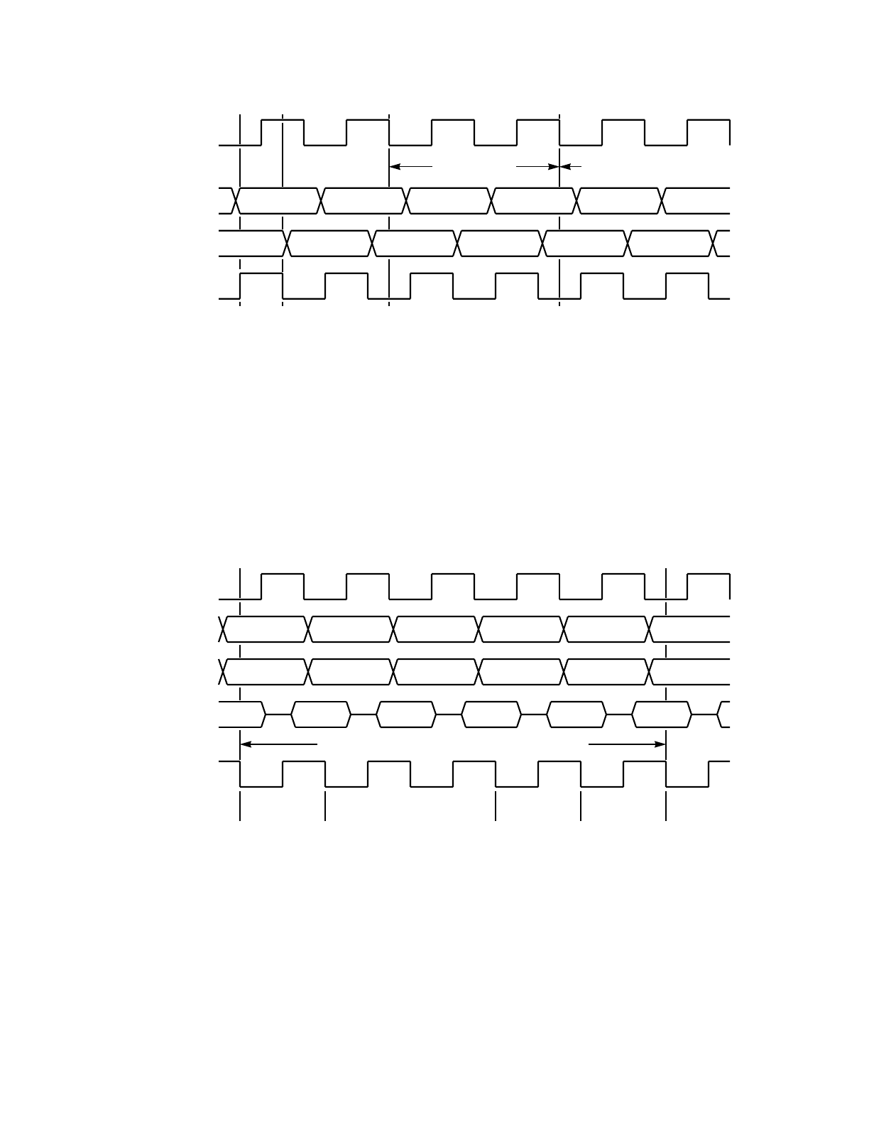
MOTOROLA MAIN TIMER AND REAL-TIME INTERRUPT M68HC11
10-40 REFERENCE MANUAL
Figure 10-13 Timer Counter as MCU Leaves Reset
Figure 10-14 shows timing details for a read of TCNT. The address and data buses
shown in Figure 10-14 are internal buses and have different timing than the more fa-
miliar external buses. These internal buses were used because it is much more difficult
to understand what is occurring from the external address and data buses.
Figure 10-14 Timer Counter Read — Cycle-by-Cycle Analysis
Figure 10-14 shows a cycle-by-cycle view of these internal buses for a double-byte
read instruction (LDD TCNT). When the upper byte of TCNT is read in the fourth cycle
of the LDD instruction, the current value of the timer isn+3.Thelow-order half of the
timer is passed through a normally transparent latch. This latch is frozen for one cycle
after every high-byte read of TCNT so that a double-byte read can read the low-order
E
ADDRESS BUS
PH2
TIMER COUNT
VECTOR FETCH
FFFE FFFE VECTOR VECTOR+1
FFFF FFFF 0000 0001 0002 0003
FIRST USER INSTRUCTION• • •
Sequence is the same for any reset (external, COP, or clock monitor) and any mode (normal or special).
FFFE∗FFFF∗
∗
PH2
ADDRESS BUS
(INTERNAL)
E
TIMER COUNT
LDD TCNT READ TIMER COUNT (EXTENDED ADDR MODE)
NN+2N+1 N+3 N+4 N+5
OPCODE ADDR OPERAND (LO)OPERAND (HI) $100F/TCNT(LO) NEXT OPCODE
DATA BUS
(INTERNAL) LO(N+3)HI(N+3)$0E$10OPCODE
$100E/TCNT(HI)
FETCH OPCODE FETCH 16-BIT OPERAND ADDRESSREAD HIGH BYTE
OF TCNT READ LOW BYTE
OF TCNT
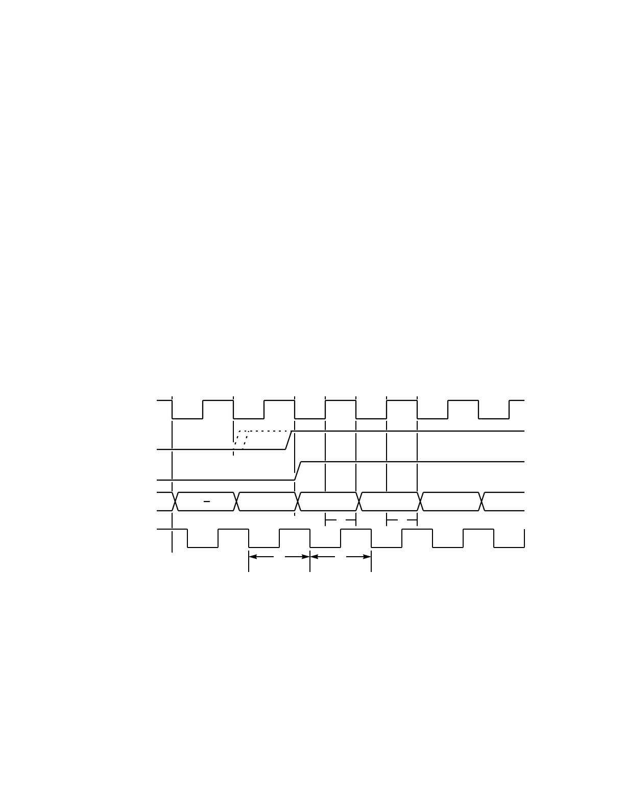
M68HC11 MAIN TIMER AND REAL-TIME INTERRUPT MOTOROLA
REFERENCE MANUAL 10-41
half that belongs with the same count state as the upper half just read. Even though
the counter has actually advanced ton+4bythelast cycle of this LDD instruction, the
value read will be the lower half of count n + 3.
The information in Figure 10-13 and Figure 10-14 can be combined to find the value
that would be returned if the LDD instruction was performed as the first instruction after
reset — that is, if the reset vector pointed directly to the LDD instruction. The value
read will always be $0005.
The prescaler is built around a divided by 16 counter. When a new value is written to
the prescaler control bits (PR1, PR0) in the TMSK2 register, the clocking rate to the
main timer changes to the new rate at the next $F–$0 transition of this internal 4-bit
prescaler counter.
Figure 10-15 shows timing details for an input capture. Input-capture timing is not af-
fected by a prescale factor; thus, this figure only shows the divided by one case. This
figure also only shows the case where the input-capture function is configured to de-
tect a rising edge. Again, the polarity of the edge is not important to the timing.
The normal sequence of events in an input capture is as follows:
1. Asynchronously detect an edge at the ICx pin.
2. Set the ICxF bit at the next falling edge of the internal PH2 clock.
3. Transfer the current timer count to the 16-bit TICx register during the next PH2
logic high.
Figure 10-15 Input-Capture Timing Details
If the cycle at [4] happens to be a high-byte read of the TlCx register (which would be
unusual), the transfer at [3] will be delayed until [6] so the transfer will not corrupt a
double-byte read at cycles [4] and [5].
Figure 10-16 shows two timing situations related to output compares. A normal com-
pare match is shown at [1]; a compare inhibit situation is shown at [4].
PH2
ICxF
E
TIMER COUNT N 1 N+1N N+2 N+3 N+4
ICx PIN
READ TICx (HI) READ TICx (LO)
[4] [5]
[1]
[2]
[3] [6]
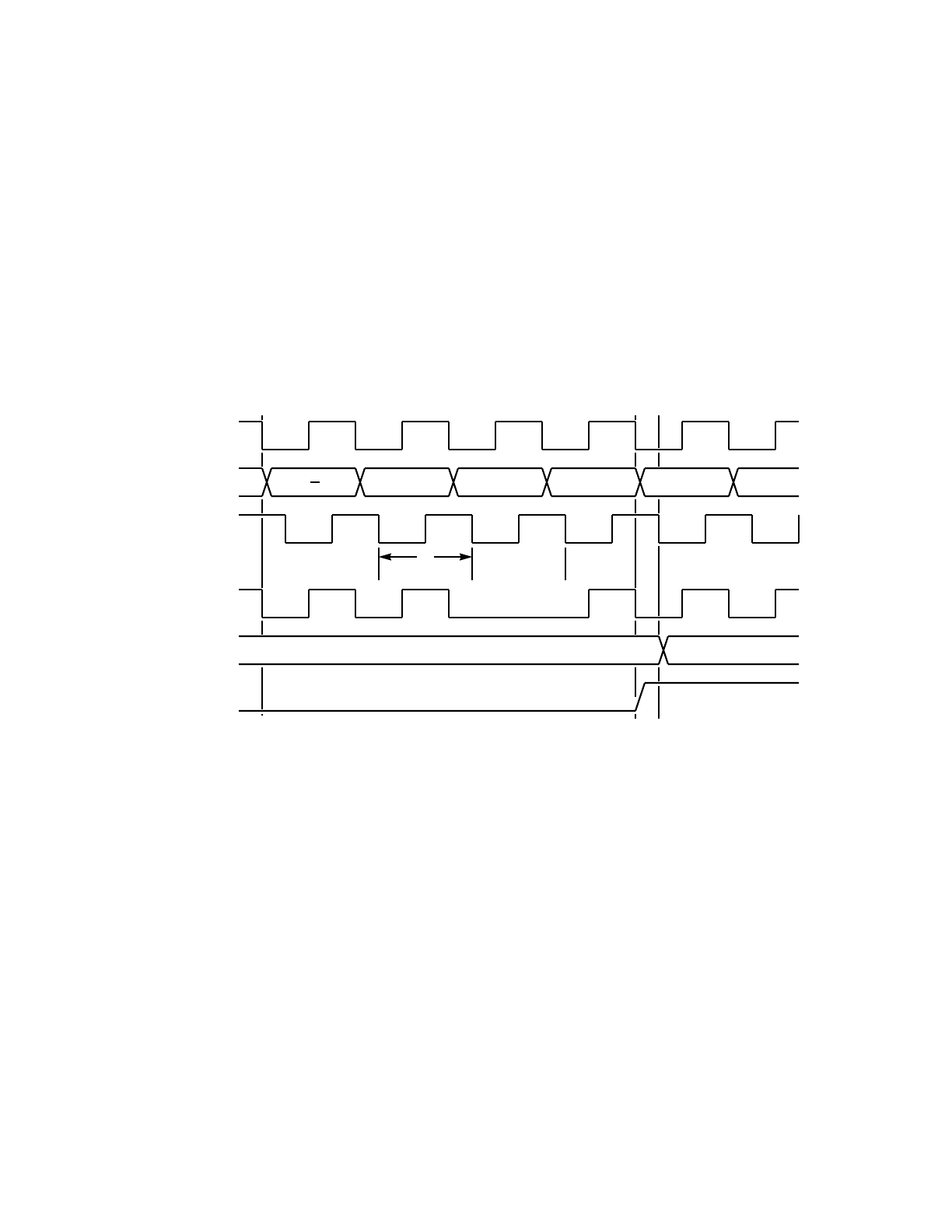
MOTOROLA MAIN TIMER AND REAL-TIME INTERRUPT M68HC11
10-42 REFERENCE MANUAL
In the normal compare match situation, the timer count is compared to the value in a
TOCx register during PH2 high. Timer counting occurs at the falling edges of PH2 to
prevent interference between counting and comparisons. PH2 is an internal clock that
leads E by 90°. When the match is detected [1], OCxF is set at the falling edge PH2
where the match was true. The pin-state change (if any) is delayed by another quarter
cycle so changes will occur at the falling edge of the E clock. If there were a prescale
factor, the compare true would occur during the first PH2 cycle where the count
matched the TOCx value. Additional matches would be inhibited until the next timer
clock or until TOCx is written. This inhibit mechanism protects against multiple com-
pare matches during a prescaled timer count (the TOCx register actually matches the
timer count for several PH2 cycles when there is a prescale factor). In the unlikely case
of a big prescale factor (e.g., ÷16) and a match at the start of count $nnnn, if the user
wrote $nnnn to the TOCx register while the count was still $nnnn, the output-compare
actions would be retriggered.
Figure 10-16 Output-Compare Timing Details
At [4] in Figure 10-16, the one-cycle compare inhibit results from a write to TOCx dur-
ing cycle [3]. This inhibit mechanism prevents an erroneous compare during the write
to the low-order half of TOCx. If the output compare were not inhibited here, the TOCx
register would contain an erroneous value composed of the new high byte written at
[3] and the low byte from the former value in TOCx. This inhibit mechanism is separate
from the compare mechanism discussed in the previous paragraph.
10.6 Listing of Timer Examples
The following listing is a composite of timer section Examples 10–1 through 10–7.
Since many of the references and equates are common for all the examples, it saves
space to group them. All the examples can be assembled and loaded into an EVB
board for evaluation at the same time. In general, the user must set up some initial sig-
nals and variables, and then execute an EVB "go" command to start each example
routine.
TIMER COUNT N 1 N+1N N+2 N+3 N+4
PH2
E
WRITE TOCx (HI) WRITE TOCx (LO)
OCx PIN
[3]
[1]
OCxF
[2]
COMPARE
ENABLE MATCH[4]
PREVIOUS PIN STATE NEW PIN STATE

M68HC11 MAIN TIMER AND REAL-TIME INTERRUPT MOTOROLA
REFERENCE MANUAL 10-43
Listing - Timer Examples Sheet 1 of 16
*****
* This listing contains all Examples for Reference Manual Section 10
*****
* TIMER EXAMPLE 10–1
** Equates Registers will be addressed with Ind,X mode
*
1000 REGBAS EQU $1000 Starting address for register block
0004 PORTB EQU $04 Output port B
000c OC1M EQU $0C OClM7,OClM6,OClM5,OClM4;OClM3,-,-,-
000d OC1D EQU $0D OClD7,OClD6,OClD5,OClD4;OClD3,-,-,-
000e TCNT EQU $0E Free running counter (16 bit)
0010 TIC1 EQU $10 IC1 register (16 bit)
0016 TOC1 EQU $16 OC1 register (16 bit)
0018 TOC2 EQU $18 OC2 register (16 bit)
001a TOC3 EQU $1A OC3 register (16 bit)
0020 TCTL1 EQU $20 OM2,OL2,OM3,OL3;OM4,OL4,OM5,OL5
0021 TCTL2 EQU $21 -,-,EDGlB,EDG-
lA;EDG2B,EDG2A,EDG3B,EDG3A
0022 TMSK1 EQU $22
OC1I,OC2I,OC3I,OC4I;OC51,IC1I,IC2I,IC3I
0023 TFLG1 EQU $23
OC1F,OC2F,OC3F,OC4F;OC5F,IC1F,IC2F,IC3F
0024 TMSK2 EQU $24 TOI,RTII,PAOVI,PAII;-,-,PR1,PR0
0025 TFLG2 EQU $25 TOF,RTIF,PAOVF,PAIF;-,-,-,-
*** EVB Routine Addresses & Pseudo Vector Equates
ffb8 .OUTA EQU $FFB8 Print character in A-reg
ffc4 .OUTCRL EQU $FFC4 Output <cr><lf>
ffca .OUTSTO EQU $FFCA Output Msg seg (no <cr,lf>)
ffc7 .OUTSTR EQU $FFC7 Output Msg w/leading <cr,lf>
00e8 PVIC1 EQU $00E8 EVB Pseudo Vector for IC1
00d0 PVTOF EQU $00D0 EVB Pseudo Vector for TOF
00dc PVOC2 EQU $00DC EVB Pseudo Vector for OC2
00df PVOC1 EQU $00DF EVB Pseudo Vector for OC1
*** RAM Variable Assignments
d000 ORG $D000 Start variables in EVB RAM (upper
half)
d000 HDLY RMB 2 Half-cycle delay (in 0.5µS incre-
ments)
d002 PWMP1P RMB 1 1% of PWM period (1 to 256 cyc) Ex 10-
7
d003 PWMDC1 RMB 1 Duty cycle for PWM signal at OC2 pin
d004 PWMDC2 RMB 1 Duty cycle for PWM signal at OC3 pin
d005 IC1DUN RMB 1 flag: 0-not done,l-pulse measured
d006 IC1MOD RMB 1 s/w mode flag: FF-off,0-1st,1-last
edge
d007 OVCNT1 RMB 1 Overflow cnt (upper 8 bits of result)
d008 RES1 RMB 2 Pulse Width in cycles (16 bits)
d00a HTEMP RMB 3 Temp for H6TOD8 (3 bytes)
d00d FRSTE RMB 2 Time of first edge (16 bits)
d00f PERC RMB 2 Period in cycles (16 bits)
d011 TEMP1 RMB 2 Temp for conversion (16 bits)

MOTOROLA MAIN TIMER AND REAL-TIME INTERRUPT M68HC11
10-44 REFERENCE MANUAL
d013 FREQH RMB 2 Freq in Hex (16 bits)
d015 HPW RMB 2 Pulse Width (16 bits hex)
d017 DBUFR RMB 8 Decimal result buffer (8 bytes ASCII)
* Some routines use only first 5 bytes of DBUFR
d01f PWMPER RMB 2 Period of PWM signals in (cycles)
d021 OFFHI RMB 2 OC2 high offset (calculated)
d023 OFFID RMB 2 OC2 low offset (calculated)

M68HC11 MAIN TIMER AND REAL-TIME INTERRUPT MOTOROLA
REFERENCE MANUAL 10-45
Listing - Timer Examples Sheet 2 of 16
c000 ORG $C000 Prog starts in EVB RAM at $C000
* TIMER EXAMPLE 10–1 (a) Measuring Period with Input Capture
*
* Uses polling rather than interrupts.
* Measures period between two rising edges at IC1 pin
* Overflows not considered so max period is 65,535 cyc
* Min period measurable with this program is about 27 cyc
*
* This program runs on an EVB board and displays results
* on the EVB terminal display.
***
OPT c
c000 8e 00 47 [3] PERTOP LDS # $0047 Top of User’s stack area on EVB
c003 ce 10 00 [3] LDX #REGBAS Point to register block
c006 86 10 [2] LDAA #%00010000
c008 a7 21 [4] STAA TCTL2,X EDGlB:EDGlA - 0:1, rising edges
c00a 86 04 [2] LDAA # $04
c00c a7 23 [4] STAA TFLG1,X Clear any old OC1 flag
* Ready to detect first rising edge
c00e 1f 23 04 fc[7] BRCLR TFLG1,X $04 * Loop here until edge
* First edge detected
c012 ec 10 [5] LDD TIC1,X Read time of first edge
c014 fd d0 0d [5] STD FRSTE Save first capture value
c017 86 04 [2] LDAA # $04
c019 a7 23 [4] STAA TFLG1,X Clear IC1F before next edge
* Ready to capture time of second edge
c01b 1f 23 04 fc[7] BRCLR TFLG1,X $04 * Loop here until edge
* Second edge detected
c01f ec 10 [5] LDD TIC1,X Read time of second edge
c021 b3 d0 0d [6] SUBD FRSTE 2nd - lst -> D
c024 fd d0 0f [5] STD PERC Save result (period in cycs)
* The period of the signal at PA2/IC1 pin has been
* measured and the time is stored at “PERC” as a 16-bit
* hex number representing the number of CPU bus cycles
* that elapsed between two rising edges
* TIMER EXAMPLE 10–1 (b) Changing Period to Frequency
*
* The period found in example 10-la is expressed as a number
* of bus cycles (@E-2MHz, 1 bus cycle=0.5µS) and it is
* currently in the D-reg and at “PERC”. Values < or = $20
* will be considered too small (freq too high) to be
* accurately measured with this program and will be trapped
* out to make the period to frequency conversion program easier.
* $0021 corresponds to 60,606 Hz, $FFFF is 30.5 Hz.
***

MOTOROLA MAIN TIMER AND REAL-TIME INTERRUPT M68HC11
10-46 REFERENCE MANUAL
Listing — Timer Examples Sheet 3 of 16
c027 fe d0 0f [5] LDX PERC Period in cycles (16 bits)
c02a 1a 83 00 20[5] CPD #32 ($20) Check against min allowed
c02e 22 03 [3] BHI OKP Skip if OK
c030 7e c0 88 [3] JMP OUTRNG Else go say it was too small
c033 cc 00 20 [3] OKP LDD #32 X-period; D-32
c036 03 [41] FDIV D/X -> X; r -> D
c037 ff d0 11 [5] STX TEMP1
* (Freq*16)+1,000,000; radix left of MSB
*
* We now have frequency but it isn’t in a good displayable
* form yet. If we move the binary radix 16 places to the right
* we would have a 16-bit integer representing
* E(2**20)/(10**6) x freq] or [((1,048,576)/(1,000,000))*freq).
* By adding and subtracting binary multiples of the freq we
* will arrive at [((1,000,000)/(1,000,000))*freq] (or just frequency)
*
* 1,048,576 16-bit starting value ((2**20)freq)+(10**6)
* - 32,768 2**15
* - 16,384 2**14
* + 512 2**9
* + 64 2**6
* = 1,000,000 * freq
*
* The limitation of 33 ($21) cycles min was selected so
* (1,048,576/1,000,000)*freq would fit in 16 bits so we would
* only need 1 FDIV, Although it is pretty easy to extend the
* precision of an FDIV
*
* The partial results which are added and subtracted in this
* program may have an error of ± LSB ea. because I truncated
* rather than rounding.
*
c03a fc d0 11 [5] LDD TEMP1 (2**20)f; where f=freq+(10**6)
c03d 04 [3] LSRD
c03e 04 [3] LSRD
c03f 04 [3] LSRD A=(2**9)f; D=(2**17)f
c040 7f d0 13 [6] CLR FREQH Clr upper half of hex freq loc.
c043 b7 d0 14 [4] STAA FREQH+1 FREQH is a temp = 512f
c046 04 [3] LSRD
c047 04 [3] LSRD now D=(2**15)f or 32,768f
c048 fd d0 11 [5] STD TEMP1 Needs to be in mem for subtract
c04b 8f [3] XGDX D=(2**20)f; X=(2**15)f
c04c b3 d0 11 [6] SUBD TEMP1 1st subtraction (-32K)
c04f 8f [3] XGDX Working result -> X; D=(2**15)f
c050 04 [3] LSRD A=(2**6)f; D=(2**14)f
c051 fd d0 11 [5] STD TEMP1 Put in mem so you can subtract
c054 bb d0 14 [4] ADDA FREQH+1 (512+64)f
c057 b7 d0 14 [4] STAA FREQH+1 Update low half of FREQH
c05a 8f [3] XGDX D=1,015,808*f; X=junk
c05b b3 d0 11 [6] SUBD TEMP1 999,424*f
c05e f3 d0 13 [6] ADDD FREQH 1,000,000*f = frequency
c061 fd d0 13 [5] STD FREQH Save the 16-bit binary result

M68HC11 MAIN TIMER AND REAL-TIME INTERRUPT MOTOROLA
REFERENCE MANUAL 10-47
Listing — Timer Examples Sheet 4 of 16
* Since most of us don’t think in hexadecimal, let’s
* change to decimal before printing. The subroutine
* (HTODP) is shown at the end of this listing.
*
* The display will look like...
*
*ppppp Cyc fffff Hz --- or like---
*Freq. is too high
*
* where ppppp is period in cycles & fffff is freq.
* (decimal)
*
* EVB subroutines will be used and when done we will
* jump back to the beginning and repeat continuously.
*
c064 bd ff c4 [6] JSR .OUTCRL Print a <cr,lf>
c067 ce d0 0f [3] LDX #PERC Point at hex period
c06a bd c3 33 [6] JSR HTOD Convert to 5 digit decimal
c06d bd c2 df [6] JSR P5DEC Print 5 digit decimal
c070 ce c3 d3 [3] LDX #MSGCYC Point at “ Cycles ”
c073 bd ff ca [6] JSR .OUTSTO Print message segment
c076 ce d0 13 [3] LDX #FREQH Point at hex frequency
c079 bd c3 33 [6] JSR HTOD Convert to 5 digit decimal
c07c bd c2 df [6] JSR P5DEC Print 5 digit decimal
c07f ce c3 e0 [3] LDX #MSGHZ Point at “ Hz”
c082 bd ff ca [6] JSR .OUTSTO Print message segment
c085 7e c0 00 [3] JTOP JMP PERTOP To top & measure another period
c088 ce c3 e4 [3] OUTRNG LDX #MSGER1 Point at "Freq. is too high"
c08b bd ff c7 [6] JSR .OUTSTR Print msg w/leading <cr,lf>
c08e 20 f5 [3] BRA JTOP To top & measure another period
*
********* END Ex 10-1b
***
* TIMER EXAMPLE 10-2 Measuring Pulses With Input Capture
*
* Uses interrupts.
* Measures time between a rising edge and a falling edge
* (period of a positive pulse) at the IC1 pin.
* Overflows not considered so max is 65,536 cyc
* Min time measurable with this program is about __ cyc
*
* This program rune on an EVB board and displays results
* on the EVB terminal display.
***
* Initialization Portion
*
c090 8e 00 47 [3] PWINZ LDS # $0047 Top of User’s stack area on EVB
c093 86 7e [2] LDAA # $7E Jump (extended) Opcode
c095 97 e8 [3] STAA PVIC1 IC1 Pseudo Vector
c097 ce c0 d8 [3] LDX #SV2IC1 Address of IC1 service routine
c09a df e9 [4] STX PVIC1+1 Finish JMP inst to IC1 routine

MOTOROLA MAIN TIMER AND REAL-TIME INTERRUPT M68HC11
10-48 REFERENCE MANUAL
Listing - Timer Examples Sheet 5 of 16
* Main Program Portion of Pulse Width program
*
c09c ce 10 00 [3] PWTOP LDX #REGBAS Point to register block
c09f 86 10 [2] LDAA #%00010000 Top of Main for PW24 prog
c0a1 a7 21 [4] STAA TCTL2,x EDG1B:EDG1A=0:l IC1 rising edge
c0a3 86 ff [2] LDAA # $FF
c0a5 b7 d0 06 [4] STAA IC1MOD FF-IC1 off; 0-lst; 1-last edge
c0a8 7f d0 05 [6] CLR IC1DUN Signal pulse not done
c0ab 1d 23 fb [7] BCLR TFLG1,X $FB clear IC1F (if any)
c0ae 1c 22 04 [7] BSET TMSK1,X $04 enable IC1 interrupts
c0b1 0e [2] CLI Enable Interrupts
c0b2 b6 d0 05 [4] WAITL2 LDAA IC1DUN Sets after pulse done
c0b5 27 fb [3] BEQ WAITL2 Loop till pulse has been timed
c0b7 0f [2] SEI Pulse done, disable interrupts
* Display pulse width as xx,xxx mS (32,768 max)
c0b8 bd ff c4 [6] JSR .OUTCRL Begin printing result
c0bb fc d0 15 [5] LDD HPW number of cyc (0.5µS/cyc)
c0be 04 [3] LSRD 16-bit +2 to change to µS
c0bf 24 03 [3] BCC ARNUP2 ? need to round result ?
c0c1 c3 00 01 [4] ADDD #1 yes; round up
c0c4 fd d0 15 [5] ARNUP2 STD HPW Update hex Pulse width
c0c7 ce d0 15 [3] LDX #HPW Point at hex Pulse width
c0ca bd c3 33 [6] JSR HTOD Convert to 5 digit decimal
c0cd bd c2 df [6] JSR P5DEC Print 5 digit decimal
c0d0 ce c3 f6 [3] LDX #MSGMS Point at rest of display line
c0d3 bd ff ca [6] JSR .OUTSTO Print “ milliseconds”
c0d6 20 c4 [3] BRA PWTOP Goto top of main & repeat
*
* END of Main Program Portion
***
* SV2IC1 - Input Capture 1 service routine
*
* Called first when a rising edge is detected and again
* when a falling edge is detected.
***
c0d8 ce 10 00 [3] SV2IC1 LDX #REGBAS point at top of register block
c0db 7c d0 06 [6] INC IC1MOD $FF->0 at 1st edge; 0->1 at 2nd
c0de 26 0d [3] BNE NO1ST2 if not 0, this is trailing edge
* Process leading edge of pulse
c0e0 ec 10 [5] LDD TIC1,X read time of first edge
c0e2 fd d0 0d [5] STD FRSTE save till next capture
* Reconfigure IC1 for trailing falling edge
c0e5 1d 21 30 [7] BCLR TCTL2,X $30 EDG1B:EDG1A->0:0
c0e8 1c 21 20 [7] BSET TCTL2,X $20 EDG1B:EDG1A->1:0
c0eb 20 10 [3] BRA OU2IC1 done processing first edge
* Process trailing edge of pulse
c0ed ec 10 [5] NO1ST2 LDD TIC1,X get time of trailing edge
c0ef b3 d0 0d [6] SUBD FRSTE time of last minus time of 1st
c0f2 fd d0 15 [5] STD HPW update result
c0f5 1d 21 30 [7] BCLR TCTL2,X $30 disable IC1
c0f8 86 01 [2] LDAA #1
c0fa b7 d0 05 [4] STAA IC1DUN signal pulse measured
c0fd 1d 23 fb [7] OU2IC1 BCLR TFLG1,X $FB clear IC1F
c100 3b [12] RTI **Return from IC1 service**
*****END Ex 10-2

M68HC11 MAIN TIMER AND REAL-TIME INTERRUPT MOTOROLA
REFERENCE MANUAL 10-49
Listing - Timer Examples Sheet 6 of 16
* TIMER EXAMPLE 10-3 Measuring Long Periods with IC
*
* Uses interrupts.
* Measures period between two rising edges at the IC1 pin.
* Overflows are counted so max is 16,777,215 cyc (≈8.38 Sec)
* min time measurable with this program is about 70 cyc
*
* This program runs on an EVB board and displays results
* on the EVB terminal display.
***
* Initialization Portion
*
c101 8e 00 47 [3] P24INZ LDS # $0047 Top of User’s stack area on EVB
c104 86 7e [2] LDAA # $7E Jump (extended) Opcode
c106 97 d0 [3] STAA PVTOF TOF Pseudo Vector see manual
c108 97 e8 [3] STAA PVIC1 IC1 Pseudo Vector
c10a ce c1 71 [3] LDX #SV3TOF Address of TOF service routine
c10d df d1 [4] STX PVTOF+1 Finish JMP inst to TOF routine
c10f ce c1 7f [3] LDX #SV3IC1 Address of IC1 service routine
c112 df e9 [4] STX PVIC1+1 Finish JMP inst to IC1 routine
* Main Program Portion of PER24 program
*
c114 ce 10 00 [3] PER24T LDX #REGBAS Point to register block
c117 86 10 [2] LDAA #%00010000 Top of Main for PER24 prog
c119 a7 21 [4] STAA TCTL2,X EDG1B:EDG1A=0:l IC1 rising edge
c11b 86 ff [2] LDAA # $FF
c11d b7 d0 06 [4] STAA IC1MOD FF-IC1 off; 0-1st; 1-last edge
c120 7f d0 05 [6] CLR IC1DUN Signal period not done
c123 1d 23 fb [7] BCLR TFLG1,X $FB clear IC1F (if any)
c126 1d 25 7f [7] BCLR TFLG2,X $7F clear TOF (if any)
c129 1c 22 04 [7] BSET TMSK1,X $04 enable IC1 interrupts
c12c 1c 24 80 [7] BSET TMSK2,X $80 enable TOF interrupts
c12f 0e [2] CLI Enable Interrupts
c130 b6 d0 05 [4] WAITL3 LDAA IC1DUN Sets after period done
c133 27 fb [3] BEQ WAITL3 Loop till period has been timed
c135 0f [2] SEI Done, disable interrupts
* Display period as x.xxxxxx Seconds (to nearest µS)
c136 ce d0 07 [3] LDX #OVCNT1 Point at hi byte of 6 digit hex
c139 64 00 [6] LSR O,x 24-bit +2 to change to µS
c13b 66 01 [6] ROR 1,X (lcyc=0.5µS)
c13d 66 02 [6] ROR 2,x RORs include carry
c13f 24 0a [3] BCC ARNUP3 ? need to round result ?
c141 6c 02 [6] INC 2,X yes; round up
c143 26 06 [3] BNE ARNUP3 carry to middle byte ?
c145 6c 01 [6] INC 1,x yes
c147 26 02 [3] BNE ARNUP3 carry to high byte ?
c149 6c 00 [6] INC 0,X yes
c14b bd c3 6c [6] ARNUP3 JSR H6TOD8 Convert to 8 digit decimal
c14e bd ff c4 [6] JSR .OUTCRL Begin printing result

MOTOROLA MAIN TIMER AND REAL-TIME INTERRUPT M68HC11
10-50 REFERENCE MANUAL
Listing - Timer Examples Sheet 7 of 16
c151 ce d0 18 [3] LDX #DBUFR+1 Start at 2nd digit (1st is 0)
c154 a6 00 [4] LDAA 0,X Seconds digit
c156 bd ff b8 [6] JSR .OUTA Print
c159 86 2e [2] LDAA #’.’ ASCII period
c15b bd ff b8 [6] JSR .OUTA Print
c15e 08 [3] DUMPLP INX Advance pointer to next digit
c15f a6 00 [4] LDAA 0,X get digit
c161 bd ff b8 [6] JSR .OUTA Print it
c164 8c d0 1e [4] CPX #DBUFR+7 Was that the last ?
c167 26 f5 [3] BNE DUMPLP If not continue
c169 ce c4 04 [3] LDX #MSGSEC Point at rest of display line
c16c bd ff ca [6] JSR .OUTSTO Print “Seconds”
c16f 20 a3 [3] BRA PER24T Goto top of main & repeat
*
* END of Main Program Portion
***
* SV3TOF - Timer Overflow service routine
*
* Called whenever any timer overflow is detected. if
* the IC1 period measurement is in progress (IC1MOD
* positive) then the overflow counter (upper 8-bits of
* period) is incremented.
***
c171 7d d0 06 [6] SV3TOF TST IC1MOD if 0 or 1 IC1 active-count TOFs
c174 2b 03 [3] BMI OU3TOF if neg, IC1 not active
c176 7c d0 07 [6] INC OVCNT1 increment IC1 overflow count
c179 86 80 [2] OU3TOF LDAA # $80
c17b b7 10 25 [4] STAA REGBAS+TFLG2Clear overflow flag
c17e 3b [12] RTI **Return from TOF service**
***
* SV3IC1 - Input Capture 1 service routine
*
* Called first when a rising edge is detected and again
* when another rising edge is detected.
***
c17f ce 10 00 [3] SV3IC1 LDX #REGBAS point at top of register block
c182 7c d0 06 [6] INC IC1MOD $FF->0 at 1st edge; 0->1 at 2nd
c185 26 13 [3] BNE NO1ST3 if not 0, this is second edge
* Process first edge of period
c187 7f d0 07 [6] CLR OVCNT1 Zero the overflow count
c18a ec 10 [5] LDD TIC1,X Read time of first edge
c18c fd d0 08 [5] STD RES1 Save till next capture
c18f 2b 27 [3] BMI OU3IC1 Done if IC was before any TOF
c191 a6 25 [4] LDAA TFLG2,X Check for TOF in MSB
c193 2a 23 [3] BPL OU3IC1 If no overflow, you’re done
c195 7a d0 07 [6] DEC OVCNT1 This TOF shouldn’t count
* decrement OVCNT1 to -1....
* TOF svc routine will inc back to zero
c198 20 1e [3] BRA OU3IC1 Done processing first edge

M68HC11 MAIN TIMER AND REAL-TIME INTERRUPT MOTOROLA
REFERENCE MANUAL 10-51
Listing - Timer Examples Sheet 8 of 16
* Process second edge of period
c19a ec 10 [5] NO1ST3 LDD TIC1,X Get time of second edge
c19c 2b 07 [3] BMI ARNOV1 If MSB=1, skip TOF check
c19e 6d 25 [6] TST TFLG2,X Check for overflow
c1a0 2a 03 [3] BPL ARNOV1 If no TOF, skip increment
c1a2 7c d0 07 [6] INC OVCNT1 TOF was before edge so count it
c1a5 b3 d0 08 [6] ARNOV1 SUBD RES1 Time of last minus time of 1st
c1a8 fd d0 08 [5] STD RES1 Update result
c1ab 24 03 [3] BCC RES1OK Check for borrow
c1ad 7a d0 07 [6] DEC OVCNT1 If borrow, fix overflow count
c1b0 1d 21 30 [7] RES1OK BCLR TCTL2,X $30 Disable IC1
c1b3 86 01 [2] LDAA #1
c1b5 b7 d0 05 [4] STAA IC1DUN Signal period measured
c1b8 1d 23 fb [7] OU3IC1 BCLR TFLG1,X $FB Clear IC1F
c1bb 3b [12] RTI **Return from IC1 service**
*
*** END Ex 10-3
* TIMER EXAMPLE 10-4 Simple Output Compare Example
*
* Exl0-4 uses polled mode.
* Generate a 10mS period like you would use to time an EE write
* but rather than wear out the EEPROM just change an output pin
*
* Example 10-4 runs on an EVB board and drives PB0 high for
* 10mS once every 30mS so you can see on an oscilloscope.
***
c1bc ce 10 00 [3] INZA LDX #REGBAS Point to register block
c1bf 86 80 [2] LDAA # $80
c1c1 a7 23 [4] STAA TFLG1,X Clear any pending OC1F flag
c1c3 6f 04 [6] CLR PORTB,X Initialize port B to zeros
c1c5 86 01 [2] TOP4A LDAA #1 Top of Ex10-4a
c1c7 a7 04 [4] STAA PORTB,X Set LSB of port B
* This is where the 10mS delay part actually starts
*
c1c9 ec 0e [5] LDD TCNT,X Get current timer count
c1cb c3 4e 20 [4] ADDD #20000 What will count be in lOmS?
c1ce ed 16 [5] STD TOC1,X Set OC1 to trigger then
c1d0 1f 23 80 fc[7] LP1 BRCLR TFLG1,X $80 LP1 Loop here till OClF=l
*
*Delay is actually done here; rest is just support
c1d4 1d 23 7f [7] BCLR TFLG1,X $7F Clear OC1F
c1d7 6f 04 [6] CLR PORTB,X Clear PB0 pin
c1d9 18 ce 16 4e[4] LDY #5710 5710*(7≈/loop)= about 2OmS
c1dd 18 09 [4] DLP1 DEY Top of software delay loop
c1df 26 fc [3] BNE DLP1 Loop ’till Y is zero
c1e1 20 e2 [3] BRA TOP4A Repeat continuously for O-scope
*
*****END Ex 10-4

MOTOROLA MAIN TIMER AND REAL-TIME INTERRUPT M68HC11
10-52 REFERENCE MANUAL
Listing - Timer Examples Sheet 9 of 16
***
* TIMER EXAMPLE 10-5 Square wave using Output Compare
*
* Ex10-5 uses interrupts.
* Generate a square wave at the PA6 output pin using OC2
*
* This program runs on an EVB board. The half-cycle delay
* time is entered into the double byte variable "HDLY" at
* $D000,D001 with a memory modify before going to the program.
***
c1e3 8e 00 47 [3] TOP5 LDS # $0047 Top of User’s stack area on EVB
c1e6 86 7e [2] LDAA # $7E Jump (extended) Opcode
c1e8 97 d0 [3] STAA PVOC2 OC2 Pseudo Vector see manual
c1ea ce c1 fd [3] LDX #SV5OC2 Address of OC2 service routine
c1ed df dd [4] STX PVOC2+1 Finish JMP inst to TOF routine
c1ef ce 10 00 [3] LDX #REGBAS Point to register block
c1f2 86 40 [2] LDAA #%01000000 OM2:OL2 = 0:1
c1f4 a7 20 [4] STAA TCTL1,X Setup OC2 to toggle on compares
c1f6 a7 23 [4] STAA TFLG1,X Clear any pending OC2F
c1f8 a7 22 [4] STAA TMSK1,X Enable OC2 interrupts
c1fa 0e [2] CLI Enable Interrupts
c1fb 20 fe [3] BRA * Interrupt driven from here
***
* SV5OC2 - Output Compare 2 service routine
*
* Called at each OC2 interrupt.
***
c1fd fc d0 00 [5] SV5OC2 LDD HDLY Get delay time for 1/2 cycle
c200 e3 18 [6] ADDD TOC2,X Add to last compare value
c202 ed 18 [5] STD TOC2,X Update OC2 (schedule next edge)
c204 1d 23 bf [7] BCLR TFLG1,X $BF Clear OC2F
c207 3b [12] RTI **Return from OC2 service**
*
*****END Ex 10-5
* TIMER EXAMPLE 10-6
* OC1, OC2, and OC3 used together to produce 2 PWM signals
*
* OC1 controls two pins of port A in conjunction with OC2 and OC3
* OC1 drives the period and the scheduling of OC2 and OC3
* OC2 & OC3 automatically control pins but don’t generate interrupts
* Set "PWMP1P", "PWMDC1" & "PWMDC2" manually before running this example
* "PWMP1P" sets size of a 1% segment of PWM period (cycles)
* min PWMP1P for this program is 2 (period = 200 cycles)
* "PWMDC1" sets Duty cycle for OC2 pin in % (0 to $64 hex)
* "PWMDC2" sets Duty Cycle for OC3 pin in % (0 to $64 hex)
* Duty cycle (%) will be translated into a # of cycles offset
* and period will be calculated as (100 * PWMP1P) at prog start
* PA4 pin will toggle at each OC1 compare as a scope reference signal

M68HC11 MAIN TIMER AND REAL-TIME INTERRUPT MOTOROLA
REFERENCE MANUAL 10-53
Listing - Timer Examples Sheet 10 of 16
* Produces high going PWM signals of the period and duty cycle specified
* Note actually only produces PWMs of 50% to 100% because spec’d duty of
* 0 to 50% is changed to low going PWM w/duty cyc = [100% - spec(0-50)]
*
* This program runs on an EVB board and drives output pins.
* An oscilloscope is used to study the results.
***
c208 8e 00 47 [3] INZ6 LDS # $0047 Top of User’s stack area on EVB
c20b 86 7e [2] LDAA # $7E Jump (extended) Opcode
c20d 97 df [3] STAA PVOC1 OC1 Pseudo Vector see manual
c20f ce c2 69 [3] LDX #SV6OC1 Address of OC1 service routine
c212 df e0 [4] STX PVOC1+1 Finish JMP inst to OC1 routine
c214 ce 10 00 [3] LDX #REGBAS Point to register block
c217 86 50 [2] LDAA #%01010000 OMx:OLx = 0:1 for toggle
c219 a7 20 [4] STAA TCTL1,X OC2 and OC3 for toggle
c21b 86 70 [2] LDAA #%01110000 OC1M6,5, & 4 = 1
c21d a7 0c [4] STAA OC1M,X Control OC2/PA6, OC3/PA5, & PA4
c21f 5f [2] CLRB Build OC1D initial value in B
c220 b6 d0 03 [4] LDAA PWMDC1 Check for OC2 duty > or = 50%
c223 81 32 [2] CMPA #50
c225 23 02 [3] BLS ARNZ61 If<50% OC1 goes lo OC2 togls hi
c227 cb 40 [2] ADDB #%01000000 else OC1 goes high OC2 togls lo
c229 b6 d0 04 [4] ARNZ61 LDAA PWMDC2 Check for OC3 duty > or = 50%
c22c 81 32 [2] CMPA #50
c22e 23 02 [3] BLS ARNZ62 I<50% OC1 goes lo OC3 togls hi
c230 cb 20 [2] ADDB #%00100000 else OC1 goes hi, OC3 togls lo
c232 e7 0d [4] ARNZ62 STAB OC1D,X Store starting value for OC1D
* Calculate period & duty cycle as cycle count offsets
c234 b6 d0 02 [4] LDAA PWMP1P 1% of period
c237 c6 64 [2] LDAB #100
c239 3d [10] MUL 100 * PWMP1P = PWMPER
c23a fd d0 1f [5] STD PWMPER Store period
c23d ed 16 [5] STD TOC1,X Start 1st PWM per @ TCNT=PWMPER
c23f b6 d0 03 [4] LDAA PWMDC1 Calculate offset for OC2
c242 8d 12 [6] BSR CALOFF Adj duty as req’d & calc offset
c244 ed 18 [5] STD TOC2,X Schedule first OC2 toggle
c246 b6 d0 04 [4] LDAA PWMDC2 Calculate offset for OC3
c249 8d 0b [6] BSR CALOFF Adj duty as req’d & calc offset
c24b ed 1a [5] STD TOC3,X Schedule first OC3 toggle
* Finish initialization
c24d 86 80 [2] LDAA # $80
c24f a7 23 [4] STAA TFLG1,X OC1F=1 to clr any old OC1 flag
c251 a7 22 [4] STAA TMSK1,X then OC1I=1 to enable OC1 int.
c253 0e [2] CLI
c254 20 fe [3] BRA * OC1 interrupt runs PWMs now

MOTOROLA MAIN TIMER AND REAL-TIME INTERRUPT M68HC11
10-54 REFERENCE MANUAL
Listing - Timer Examples Sheet 11 of 16
*** Local subroutine to change duty cycle to offset cnt
* If duty < 50% ($32) change to 100-duty
* If duty >100% ($64) force to $64
* Finally mult by 1% of period (cyc)
* Enter with PWMDCx duty in A-reg, Return offset in D
c256 81 32 [2] CALOFF CMPA #50 Check for 0-49%
c258 24 04 [3] BHS ARN6A Around fixup
c25a 16 [2] TAB If <50% set to 100 - duty cycle
c25b 86 64 [2] LDAA #100
c25d 10 [2] SBA A-B to A
c25e 81 64 [2] ARN6A CMPA #100 Check for > 100%
c260 23 02 [3] BLS ARN6B
c262 86 64 [2] LDAA #100 If > 100% - set to 100%
c264 f6 d0 02 [4] ARN6B LDAB PWMP1P
c267 3d [10] MUL PWMP1P * adj’d duty cyc =OFFOCX
c268 39 [5] RTS **Return from CALOFF**
*
***
***
* SV6OC1 - Output Compare 1 service routine
***
c269 ce 10 00 [3] SV6OC1 LDX #REGBAS Point to register block
c26c a6 0d [4] LDAA OC1D,X Make PA4 flip @ nxt OC1 compare
c26e 88 10 [2] EORA #%00010000 Flips OC1D4 bit(PA4 pin contrl)
c270 a7 0d [4] STAA OC1D,X Update nxt OC1 auto pattern
c272 ec 18 [5] LDD TOC2,X Get last OC2 compare value
c274 f3 d0 1f [6] ADDD PWMPER Add count equiv to period
c277 ed 18 [5] STD TOC2,X Update OC2 (schedule next OC2)
c279 ec 1a [5] LDD TOC3,X Get last OC3 compare value
c27b f3 d0 1f [6] ADDD PWMPER Add count equiv to period
c27e ed 1a [5] STD TOC3,X Update OC3 (schedule next OC3)
c280 ec 16 [5] LDD TOC1,X Get last OC1 compare value
c282 f3 d0 1f [6] ADDD PWMPER Add count equiv to period
c285 ed 16 [5] STD TOC1,X Update OC1 (schedule next OCl)
c287 1d 23 7f [7] BCLR TFLG1,X $7F Clear OC1F
c28a 3b [12] RTI Return from OC1 service
*
**** END Ex 10-6
***
* TIMER EXAMPLE 10-7
* OC2 used alone to produce one PWH signal
*
* OC2 controls period and duty cycle of one port A pin
* Set “PWMP1P” & “PWMDC1” manually before running this
* example
* “PWMP1P” sets size of a 1% segment of PWM period
* (in cycles)
* “PWMDC1” sets Duty cycle for OC2 pin in % - NOTE: This
* program will not work properly with values of duty
* cycle too near 0 or 100%
* Refer to User’s Manual text for discussions
* Program calculates “OFFHI” and “OFFLO” at start

M68HC11 MAIN TIMER AND REAL-TIME INTERRUPT MOTOROLA
REFERENCE MANUAL 10-55
Listing - Timer Examples Sheet 12 of 16
* This program runs on EVB board & drives PA6/OC2 pin.
* An oscilloscope is used to study the results.
***
c28b 8e 00 47 [3] INZ7 LDS # $0047 Top of User’s stack area on EVB
c28e 86 7e [2] LDAA # $7E Jump (extended) Opcode
c290 97 d0 [3] STAA PVOC2 OC2 Pseudo Vector
c292 ce c2 c2 [3] LDX #SV7OC2 Address of OC2 service routine
c295 df dd [4] STX PVOC2+1 Finish JMP instruc to OC2 prog
c297 ce 10 00 [3] LDX #REGBAS Point to register block
c29a b6 d0 03 [4] LDAA PWMDC1 Calculate OC2 high time
c29d f6 d0 02 [4] LDAB PWMP1P 1% of period
c2a0 3d [10] MUL
* PWMP1P * duty cycle = high part of period
c2a1 fd d0 21 [5] STD OFFHI Save high offset
c2a4 b6 d0 02 [4] LDAA PWMP1P 1% of period
c2a7 c6 64 [2] LDAB #100
c2a9 3d [10] MUL 100 * PWMP1P = period
c2aa b3 d0 21 [6] SUBD OFFHI period - high time = low time
c2ad fd d0 23 [5] STD OFFLO Store low offset
* Finish initialization
c2b0 86 c0 [2] LDAA #%11000000 OM2:OL2 = 1:1 for set pin high
c2b2 a7 20 [4] STAA TCTL1,X 1st OC2 starts first high time
c2b4 cc 00 00 [3] LDD # $0000
c2b7 ed 18 [5] STD TOC2,X Start 1st PWM period @ TCNT=0
c2b9 86 40 [2] LDAA # $40
c2bb a7 23 [4] STAA TFLG1,X OC2F=1 to clr any old OC2 flag
c2bd a7 22 [4] STAA TMSK1,X then OC2I=1 to enable OC2 inter
c2bf 0e [2] CLI
c2c0 20 fe [3] BRA * OC2 interrupt runs PWM now
***
* SV7OC2 - Output Compare 2 service routine
***
c2c2 ce 10 00 [3] SV7OC2 LDX #REGBAS Point to register block
c2c5 1f 20 40 05[7] BRCLR TCTL1,X %01000000 ADDLO Which half of cyc?
c2c9 fc d0 21 [5] LDD OFFHI High part so add OFFHI to OC2
c2cc 20 03 [3] BRA UPOC2
c2ce fc d0 23 [5] ADDLO LDD OFFLO Low part so add OFFLO to OC2
c2d1 e3 18 [6] UPOC2 ADDD TOC2,X Add to last compare value
c2d3 ed 18 [5] STD TOC2,X Update OC2 (schedule next edge)
c2d5 a6 20 [4] LDAA TCTL1,X Change OL2 to setup next edge
c2d7 88 40 [2] EORA #%01000000 Inverts OL2 bit
c2d9 a7 20 [4] STAA TCTL1,X Update control reg
c2db 1d 23 bf [7] BCLR TFLG1,X $BF Clear OC2F
c2de 3b [12] RTI **Return from OC2 service**
*
***** END Ex 10-7

MOTOROLA MAIN TIMER AND REAL-TIME INTERRUPT M68HC11
10-56 REFERENCE MANUAL
Listing - Timer Examples Sheet 13 of 16
***
* General purpose subroutines
***
***
* P5DEC - Subroutine to display a five digit decimal
* number at "DBUFR".
* Prints in the form “xx,xxx” with leading zeros
* suppressed. Prints 6 columns, leading spaces,
* units always prints (0-9)
*
* Calls EVB routine ".OUTA"
* Calls "SKP1" with BSR to advance X and print a
* leading space SKP1 subroutine follows P5DEC
* All registers are unchanged upon return from P5DEC
***
c2df 3c [4] PSDEC PSHX Save registers
c2e0 37 [3] PSHB
c2e1 36 [3] PSHA
c2e2 ce d0 17 [3] LDX #DBUFR Point at decimal (MS character)
c2e5 86 30 [2] LDAA # $30 Chk for leading 0s (ASCII)
c2e7 a1 00 [4] CMPA 0,X Check 10,000s digit
c2e9 26 19 [3] BNE P10K Start at 10k digit
c2eb 8d 3d [6] BSR SKP1 INX & print a space
c2ed a1 00 [4] CMPA 0,X Chk 1,000s (A still=ASCII<sp>)
c2ef 26 19 [3] BNE P1K Start at 1k digit
c2f1 8d 37 [6] BSR SKP1 INX & print a space
c2f3 8d 35 [6] BSR SKP1 INX & print extra sp for “,”
c2f5 09 [3] DEX just wanted <sp> so back up 1
c2f6 a1 00 [4] CMPA 0,X Check 100s digit
c2f8 26 1b [3] BNE P100 Start at 100s digit
c2fa 8d 2e [6] BSR SKP1 INX & print a space
c2fc a1 00 [4] CMPA 0,X Check 10s digit
c2fe 26 1b [3] BNE P10 Start at 10s digit
c300 8d 28 [6] BSR SKP1 INX & print a space
c302 20 1d [3] BRA P1 Start at 1s digit (default)
c304 a6 00 [4] P10K LDAA 0,X 10,000s digit
c306 bd ff b8 [6] JSR OUTA Print 10,000s digit
c309 08 [3] INX Advance pointer to next digit
c30a a6 00 [4] P1K LDAA 0,X 1,000s digit
c30c bd ff b8 [6] JSR OUTA Print it
c30f 86 2c [2] LDAA #’,’ ASCII comma
c311 bd ff b8 [6] JSR OUTA Print
c314 08 [3] INX Advance pointer to next digit
c315 a6 00 [4] P100 LDAA 0,X 100s digit
c317 bd ff b8 [6] JSR .OUTA Print it
c31a 08 [3] INX Advance pointer to next digit
c31b a6 00 [4] P10 LDAA 0,X 10s digit
c31d bd ff b8 [6] JSR OUTA Print it
c320 08 [3] INX Advance pointer to next digit
c321 a6 00 [4] P1 LDAA 0,X 1s digit
c323 bd ff b8 [6] JSR OUTA Print it
c326 32 [4] PULA Restore registers
c327 33 [4] PULB
c328 38 [5] PULX
c329 39 [5] RTS **Return from P5DEC**

M68HC11 MAIN TIMER AND REAL-TIME INTERRUPT MOTOROLA
REFERENCE MANUAL 10-57
Listing - Timer Examples Sheet 14 of 16
*** Local SKP1 subroutine (called from above with BSRS)
c32a 36 [3] SKPI PSHA Save A
c32b 08 [3] INX Advance X
c32c 86 20 [2] LDAA # $20 ASCII <sp>
c32e bd ff b8 [6] JSR OUTA Print the <sp>
c331 32 [4] PULA Restore A
c332 39 [5] RTS ** Return from SKP1 **
***
*HTOD - Subroutine to convert a 16-bit hex number to a
* 5 digit decimal number.
*
* Uses 5 byte variable “DBUFR” for decimal ASCII result
* On entry X points to hex value to be converted &
* displayed
* All registers are unchanged upon return
***
c333 3c [4] HTOD PSHX Save registers
c334 37 [3] PSHB
c335 36 [3] PSHA
c336 ec 00 [5] LDD 0,X D=hex value to be converted
c338 ce 27 10 [3] LDX #10000
c33b 02 [41] IDIV freq+10,000 -> X; r -> D
c33c 8f [3] XGDX Sav r in X 10,000s digit in A:B
c33d cb 30 [2] ADDB # $30 Convert to ASCII
c33f f7 d0 17 [4] STAB DBUFR Store in decimal buffer
c342 8f [3] XGDX r back to D
c343 ce 03 e8 [3] LDX #1000
c346 02 [41] IDIV r+1,000 -> X; r -> D
c347 8f [3] XGDX Sav r in X; 1,000s digit in A:B
c348 cb 30 [2] ADDB # $30 Convert to ASCII
c34a f7 d0 18 [4] STAB DBUFR+1 Store in decimal buffer
c34d 8f [3] XGDX r back to D
c34e ce 00 64 [3] LDX #100
c351 02 [41] IDIV r+100 -> X; r -> D
c352 8f [3] XGDX Save r in X; 100s digit in A:B
c353 cb 30 [2] ADDB # $30 Convert to ASCII
c355 f7 d0 19 [4] STAB DBUFR+2 Store in decimal buffer
c358 8f [3] XGDX r back to D
c359 ce 00 0a [3] LDX #10
c35c 02 [41] IDIV r+10 -> X; r in D (B= 1s digit)
c35d cb 30 [2] ADDB # $30 Convert to ASCII
c35f f7 d0 1b [4] STAB DBUFR+4 Store to units digit
c362 8f [3] XGDX 10s digit to D (A:B)
c363 cb 30 [2] ADDB # $30 Convert to ASCII
c365 f7 d0 1a [4] STAB DBUFR+3 Store in decimal buffer
c368 32 [4] PULA Restore registers
c369 33 [4] PULB
c36a 38 [5] PULX
c36b 39 [5] RTS **Return**

MOTOROLA MAIN TIMER AND REAL-TIME INTERRUPT M68HC11
10-58 REFERENCE MANUAL
Listing - Timer Examples Sheet 15 of 16
***
*H6TOD8 - Subroutine to convert a 24-bit hex number to
* an 8 digit decimal number.
*
* Uses 3 byte variable "HTEMP" for hex working value
* Uses 8 byte variable "DBUFR" for decimal ASCII result
* On entry X points to the hex value to be converted &
* displayed
* All registers are unchanged upon return
***
c36c 18 3c [5] H6TOD8 PSHY Save registers
c36e 3c [4] PSHX
c36f 37 [3] PSHB
c370 36 [3] PSHA
c371 ec 01 [5] LDD 1,X Move hex to HTEMP to convert
c373 fd d0 0b [5] STD HTEMP+1 Two lower bytes moved
c376 a6 00 [4] LDAA 0,X Upper byte
c378 b7 d0 0a [4] STAA HTEMP
c37b 18 ce d0 17[4] LDY #DBUFR Pnt @ MS digit of decimal buf’r
c37f ce c4 0d [3] LDX #CON10M Point at first 24-bit constant
c382 4f [2] HTDLP CLRA A keeps track of # of subtracts
c383 4c [2] HLPIN INCA Inner loop; once per subtract
c384 f6 d0 0c [4] LDAB HTEMP+2 Start 24-bit subtract
c387 e0 02 [4] SUBB 2,X
c389 f7 d0 0c [4] STAB HTEMP+2 Update low byte
c38c f6 d0 0b [4] LDAB HTEMP+1 Middle byte
c38f e2 01 [4] SBCB 1,X Sub with carry
c391 f7 d0 0b [4] STAB HTEMP+1 Update middle byte
c394 f6 d0 0a [4] LDAB HTEMP High byte
c397 e2 00 [4] SBCB 0,X
c399 f7 d0 0a [4] STAB HTEMP Update high byte
c39c 24 e5 [3] BCC HLPIN If no borrow; subtract again
c39e f6 d0 0c [4] LDAB HTEMP+2 Last subtract too far; add back
c3a1 eb 02 [4] ADDB 2,X
c3a3 f7 d0 0c [4] STAB HTEMP+2 Update low byte
c3a6 f6 d0 0b [4] LDAB HTEMP+1 Middle byte
c3a9 e9 01 [4] ADCB 1,X Sub with carry
c3ab f7 d0 0b [4] STAB HTEMP+1 Update middle byte
c3ae f6 d0 0a [4] LDAB HTEMP High byte
c3b1 e9 00 [4] ADCB 0,X
c3b3 f7 d0 0a [4] STAB HTEMP Update high byte
c3b6 8b 2f [2] ADDA # $2F Convert digit to ASCII
c3b8 18 a7 00 [5] STAA 0,Y Store to decimal buffer
c3bb 18 08 [4] INY Point to next decimal digit
c3bd 08 [3] INX Point to next 24-bit const
c3be 08 [3] INX
c3bf 08 [3] INX
c3c0 8c c4 22 [4] CPX #CONEND See if done yet
c3c3 26 bd [3] BNE HTDLP If not done, do nxt digit

M68HC11 MAIN TIMER AND REAL-TIME INTERRUPT MOTOROLA
REFERENCE MANUAL 10-59
Listing - Timer Examples Sheet 16 of 16
c3c5 b6 d0 0c [4] LDAA HTEMP+2 Get 1s digit
c3c8 8b 30 [2] ADDA # $30 Convert to ASCII
c3ca 18 a7 00 [5] STAA 0,Y Store to last decimal digit
c3cd 32 [4] PULA Restore registers
c3ce 33 [4] PULB
c3cf 38 [5] PULX
c3d0 18 38 [6] PULY
c3d2 39 [5] RTS Return from H6TOD8
*
* Display Messages & Constants
*
c3d3 20 43 79 63 6c MSGCYC FCC ‘ Cycles ‘
65 73 20 20 20
20 20
c3df 04 FCB $04 End-of-message mark
c3e0 20 48 7a MSGHZ FCC ’Hz’
c3e3 04 FCB $04 End-of-message mark
c3e4 46 72 65 71 2e MSGER1 FCC ’Freq. is too high’
20 69 73 20 74
6f 6f 20 68 69
67 68
c3f5 04 FCB $04 End-of-message mark
c3f6 20 6d 69 63 72 MSGMS FCC ’microseconds’
6f 73 65 63 6f
6e 64 73
c403 04 FCB $04 End-of-message mark
c404 20 53 65 63 6f MSGSEC FCC ’Seconds’
6e 64 73
c40c 04 FCB $04 End-of-message mark
c40d 98 96 80 CON10M FCB $98,$96,$80 = 24-bit equiv of 10,000,000
c410 0f 42 40 FCB $0F,$42,$40 = 24-bit equiv of 1,000,000
c413 01 86 a0 FCB $01,$86,$A0 = 24-bit equiv of 100,000
c416 00 27 10 FCB $00,$27,$10 = 24-bit equiv of 10,000
c419 00 03 e8 FCB $00,$03,$E8 = 24-bit equiv of 1,000
c41c 00 00 64 FCB $00,$00,$64 = 24-bit equiv of 100
c41f 00 00 0a FCB $00,$00,$0A = 24-bit equiv of 10
c422 CONEND EQU *Don’t need 1s const
*END OF FILE
*0 error(s)

MOTOROLA MAIN TIMER AND REAL-TIME INTERRUPT M68HC11
10-60 REFERENCE MANUAL

M68HC11 PULSE ACCUMULATOR MOTOROLA
REFERENCE MANUAL 11-1
SECTION 11
PULSE ACCUMULATOR
The pulse accumulator, which is similar to the timers in older MC6805 MCUs, is a
much simpler system than the main timer discussed in SECTION 10 MAIN TIMER
AND REAL-TIME INTERRUPT. This system is based on an 8-bit counter and can be
configured to operate as a simple event counter or for gated time accumulation. Unlike
the main timer, the 8-bit pulse accumulator counter can be read or written at any time
(the 16-bit counter in the main timer cannot be written). Control bits allow the user to
configure and control the pulse accumulator subsystem. Two maskable interrupts are
associated with the system, each having its own controls and interrupt vector.
The port A bit 7 I/O pin (PA7/PAI/OC1) associated with the pulse accumulator can be
configured to act as a clock (event counting mode) or as a gate signal to enable a free-
running E divided by 64 clock to the 8-bit counter (gated time accumulation mode). The
alternate functions of the pulse accumulator input (PAI) pin present some interesting
application possibilities.
11.1 General Description
The pulse accumulator is an 8-bit counter/timer system that can be configured to op-
erate in either of two basic modes. In the event counting mode, the 8-bit counter is
clocked to increasing values at each active edge of the PAI pin. In the gated time ac-
cumulation mode, the 8-bit counter is clocked by a free-running E divided by 64 clock
subject to the PAI pin being active. Figure 11-1 is a simplified block diagram of the
pulse accumulator in each of these two possible modes.
Figure 11-1 Pulse Accumulator Operating Modes
Table 11-1 summarizes the important timing periods for the pulse accumulator (when
operating in gated time accumulation mode) for various common crystal rates. The for-
mulas at the bottom of the table can be used for a different crystal frequency than
those shown.
PA7/
PAI/
OC1
PIN
8-BIT COUNTER
PACNT
CLOCK
PA7/
PAI/
OC1
PIN
8-BIT COUNTER
PACNT
CLOCK
E÷ 64 CLOCK
(FROM MAIN TIMER)
PAMOD = 1
GATED-TIME ACCUMULATION MODE
PAMOD = 0
EVENT COUNTING MODE

MOTOROLA PULSE ACCUMULATOR M68HC11
11-2 REFERENCE MANUAL
The free-running E divided by 64 clock is a tap off the main timer clocking chain (see
10.2.1 Overall Clock Divider Structure and Figure 10-3). In general, any signal ap-
plied to the PAI pin is asynchronous to this E divided by 64 clock; therefore, the first
count could occur anywhere between zero and 64 E clocks after the PAI pin goes to
the chosen active level.
User software can enable the pulse accumulator system, select its mode, and deter-
mine the polarity of signals recognized at the PAI pin. Two separate interrupts are as-
sociated with the pulse accumulator system: one is generated by detection of a
selected edge at the PAI pin; the other is generated when the 8-bit counter rolls over
from $FF to $00 (overflow). Each of these interrupt sources has its own local enable
bit and its own interrupt vector; thus, no software polling is required to determine the
cause of any pulse accumulator interrupts.
11.1.1 Pulse Accumulator Block Diagram
Figure 11-2 is a functional block diagram of the pulse accumulator subsystem. The
central element of this system is an 8-bit up-counter that can be read or written at any
time. The pulse accumulator enable (PAEN) control bit enables/disables this 8-bit
counter. The pulse accumulator mode (PAMOD) bit selects the clock source to this
counter. In the event counting mode, the clock is the output of the edge detector of the
PAI pin. In the gated time accumulation mode, the clock is a free-running, internal E
divided by 64 clock ANDed (gated) with the active level of the PAI pin. The pulse ac-
cumulator edge select (PEDGE) bit controls the polarity of signals on the PAI pin that
will be recognized by the pulse accumulator system. The pulse accumulator overflow
interrupt enable (PAOVI) bit determines whether or not a pulse accumulator overflow
interrupt flag (PAOVF) will generate hardware interrupt requests. The pulse accumu-
lator input edge interrupt enable (PAII) bit determines whether or not detected edges
at the PAI pin will cause the pulse accumulator input flag (PAIF) to be set (generating
hardware interrupt requests). In addition to the PAII and PAOVI local interrupt enables,
these interrupts are subject to masking by the I bit in the condition code register in the
central processing unit (CPU). For additional information about interrupts, refer to
SECTION 5 RESETS AND INTERRUPTS.
The input buffer on the PAI pin is always connected from the pin to the pulse accumu-
lator and port A read logic, but the output buffer is enabled or disabled by the data di-
rection control bit (DDRA7) in the pulse accumulator control (PACTL) register.
Normally, when the pulse accumulator is being used, the PAI pin is configured as a
high-impedance input (DDRA7 = 0), but it is possible for software or the main timer (by
way of output compare 1) to directly control the pulse accumulator by setting DDRA7
equal to one (output). A detailed transistor-level schematic of this pin logic is shown in
Table 11-1 Pulse Accumulator Timing Periods vs. Crystal Rate
2.1 MHz 223 Hz 477 ns 30.52 µs 7.81 ms
2 MHz 8 MHz 500 ns 32 µs 8.19 ms
1 MHz 4 MHz 1 µs64µs 16.38 ms
Formula: 64(E Period) 16,384(E Period)
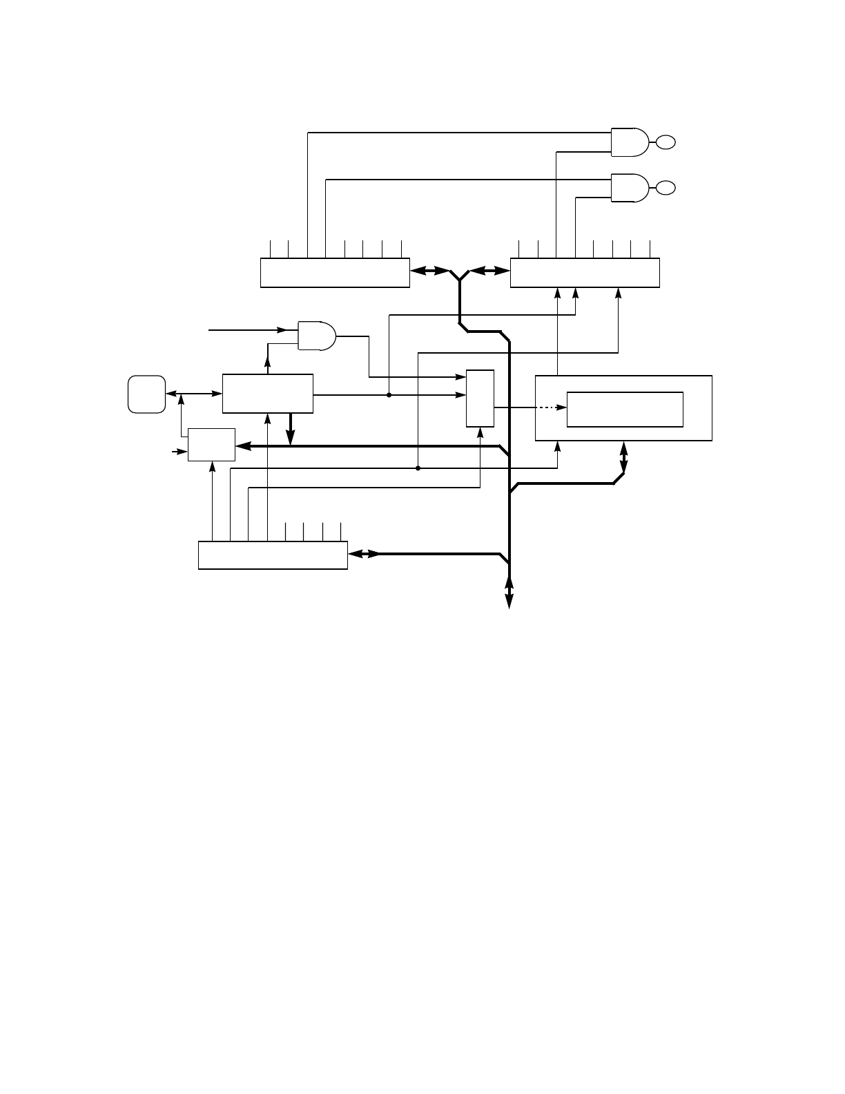
M68HC11 PULSE ACCUMULATOR MOTOROLA
REFERENCE MANUAL 11-3
SECTION 7 PARALLEL INPUT/OUTPUT.
Figure 11-2 Block Diagram of Pulse Accumulator Subsystem
11.1.2 Pulse Accumulator Control and Status Registers
Figure 11-3 shows all control and status registers related to the pulse accumulator.
Each of these registers and bits is discussed in detail in the following paragraphs.
The 8-bit pulse accumulator counter (PACNT–$1027) is not affected by reset and can
be read or written any time. Counting is synchronized to the internal PH2 clock so that
incrementing and reading occur during opposite half cycles.
PACNT
8-BIT COUNTER
2:1
MUX
PA7/
ENABLE
OVERFLOW
1
2
INTERRUPT
REQUESTS
INTERNAL
DATA BUS
INPUT BUFFER
&
EDGE DETECTION
PACTL
TFLG2TMSK2
PAOVI
PAII
DDRA7
PAEN
PAMOD
PEDGE
PAOVF
PAIF
11 PULSE ACC BLOCK
OUTPUT
BUFFER
PAI EDGE
PAEN
E÷ 64 CLOCK
(FROM MAIN TIMER)
PAI/OC1
FROM
MAIN TIMER
OC1
DISABLE
FLAG SETTING
MOTOROLA PULSE ACCUMULATOR M68HC11
11-4 REFERENCE MANUAL
Figure 11-3 Pulse Accumulator Control and Status Register Summary
The following register and paragraphs describe the pulse accumulator related bits in
the PACTL register. Bits 2 and 3 are not implemented and always read as zeros. Al-
though bits 0 and 1 are not related to the pulse accumulator, an awareness of these
real-time interrupt rate bits is necessary to prevent inadvertent change while writing to
the pulse accumulator related bits.
DDRA7 — Data Direction Control for Port A Bit 7
0 = Port A bit 7 is configured for input only (output buffer is disabled).
1 = Port A bit 7 is configured for output.
Normally when the pulse accumulator is being used, the PAI pin will be configured as
an input. In unusual cases, the PA7/PAI/OC1 pin can be configured as an output to
allow OC1 or a software output to drive the pulse accumulator system. Since the input
buffer is always connected to the pin (even when the pin is configured as an output),
any output function that is controlling the PA7 pin will also be driving the pulse accu-
mulator.
PAEN — Pulse Accumulator Enable
0 = Pulse accumulator disabled.
TMSK2 — Timer Interrupt Mask 2 Register $1024
BIT 7 654321BIT 0
TOI RTII PAOVI PAII 0 0 PR1 PR0
RESET: 00000000
TFLG2 — Timer Interrupt Flag 2 Register $1025
BIT 7 654321BIT 0
TOF RTIF PAOVF PAIF 0000
RESET: 00000000
PACTL — Pulse Accumulator Control Register $1026
BIT 7 654321BIT 0
DDRA7 PAEN PAMOD PEDGE 0 0 RTR1 RTR0
RESET: 00000000
PACNT — Pulse Accumulator Count Register $1027
BIT 7 654321BIT 0
BIT 7 ——————BIT 0
RESET: ————————
PACTL — Pulse Accumulator Control Register $1026
BIT 7 654321BIT 0
DDRA7 PAEN PAMOD PEDGE 0 0 RTR1 RTR0
RESET: 00000000

M68HC11 PULSE ACCUMULATOR MOTOROLA
REFERENCE MANUAL 11-5
1 = Pulse accumulator enabled.
When the pulse accumulator is disabled, the 8-bit counter stops counting, and pulse
accumulator interrupts are inhibited. Though the flags cannot become set, they will re-
main set if they were ones at the time the pulse accumulator was disabled.
PAMOD — Pulse Accumulator Mode Select
0 = External event counting mode (pin acts as clock).
1 = Gated time accumulation mode (pin acts as clock enable for E divided by 64
clock).
PEDGE — Pulse Accumulator Edge Select
0 = Pulse accumulator responds to falling edges (inhibit gate level is zero).
1 = Pulse accumulator responds to rising edges (inhibit gate level is one).
In gated time accumulation mode (PAMOD = 1), the PEDGE bit has added meaning.
In addition to specifying the edge polarity that causes the PAIF bit to be set, PEDGE
also controls the inhibit gate level, which disables the internal, free-running E divided
by 64 clock to the pulse accumulator counter. The PAIF interrupts occur at the trailing
edge of a gate enable signal; thus, selecting falling edges causes the free-running E
divided by 64 clock to be disabled while the PAI pin is low.
The following registers and paragraphs explain the pulse accumulator interrupt flags
and the pulse accumulator interrupt enable bits. The other bits in these registers not
related to the pulse accumulator system are discussed in SECTION 10 MAIN TIMER
AND REAL-TIME INTERRUPT.
PAOVI, PAOVF — Pulse Accumulator Overflow Interrupt Enable and Flag
The PAOVF status bit is automatically set to one each time the pulse accumulator
count rolls over from $FF to $00. This status bit is cleared by writing to the TFLG2 reg-
ister with a one in the corresponding data bit position (bit 4). The PAOVI control bit al-
lows the user to configure the pulse accumulator overflow for polled or interrupt-driven
operation but does not affect the setting or clearing of PAOVF. When PAOVI is zero,
pulse accumulator overflow interrupts are inhibited, and the system is operating in a
polled mode. In this mode, PAOVF must be polled (sampled) by user software to de-
termine when an overflow has occurred. When the PAOVI control bit is one, a hard-
ware interrupt request is generated each time PAOVF is set to one. Before leaving the
interrupt service routine, software must clear PAOVF by writing to the TFLG2 register.
For additional information, refer to 10.2.4 Tips for Clearing Timer Flags.
TMSK2 — Timer Interrupt Mask 2 Register $1024
BIT 7 654321BIT 0
TOI RTII PAOVI PAII 0 0 PR1 PR0
RESET: 00000000
TFLG2 — Timer Interrupt Flag 2 Register $1025
BIT 7 654321BIT 0
TOF RTIF PAOVF PAIF 0000
RESET: 00000000

MOTOROLA PULSE ACCUMULATOR M68HC11
11-6 REFERENCE MANUAL
PAII, PAIF — Pulse Accumulator Input Edge Interrupt Enable and Flag
The PAIF status bit is automatically set to one each time a selected edge is detected
at the PA7/PAI/OC1 pin. This status bit is cleared by writing to the TFLG2 register with
a one in the corresponding data bit position (bit 5). The PAII control bit allows the user
to configure the pulse accumulator input edge detect for polled or interrupt-driven op-
eration but does not affect the setting or clearing of the PAIF bit. When PAII is zero,
pulse accumulator input interrupts are inhibited, and the system is operating in a polled
mode. In this mode, the PAIF bit must be polled (sampled) by user software to deter-
mine when an edge has occurred. When the PAII control bit is one, a hardware inter-
rupt request is generated each time PAIF is set to one. Before leaving the interrupt
service routine, software must clear PAIF by writing to the TFLG2 register. For addi-
tional information, refer to 10.2.4 Tips for Clearing Timer Flags.
11.2 Event Counting Mode
Many microcontroller unit (MCU) applications require "things" to be counted. These
things are called events, but in real applications they might be anything: pieces on an
assembly line, cycles of an incoming signal, or units of time. To be counted by the
pulse accumulator, these things must be translated into rising or falling edges on the
PAI pin. Either edge will do because software can pick which edge will be recognized.
A trivial example of event counting might be to count pieces on an assembly line. A
light emitter/detector pair could be placed across the path of the pieces so that, as
each piece passes the sensor, the light beam is interrupted and a logic-level signal is
produced, which can be connected to the PAI pin.
11.2.1 Interrupting after N Events
By writing to the PACNT, the pulse accumulator can be set up to produce an interrupt
after N events. The trick is to write the twos complement of the number (N) to PACNT
so that the counter will overflow after N counts. If the following program sequence is
used, the PACNT will overflow after the 100th count:
---- 86 64 [2] LDAA #100 Hex ($64)
---- 40 [2] NEGA Two’s complement ($9C)
---- b7 10 27 [4] STAA PACNT Store to pulse accum counter
11.2.2 Counting More Than 256 Events
More than 256 events can be counted by using software to keep track of how many
times the PACNT overflows. Before the first event, calculate the number of overflows
needed and a value corresponding to any remainder that is left after seeing how many
whole times 256 goes into the intended count. Two cases are used as examples. In
the first case, 512 ($0200) events will be counted; in the second case, 515 ($0203)
events will be counted. In both cases, assume the desired count is in the D register.
Since D is the concatenation of the A register (upper 8 bits of D) and the B register
(lower 8 bits of D), division to see how many whole times 256 can go into the desired
count is not necessary (the A register has this count).
For case 1, two overflows are needed (there is no remainder). Zero is stored to
PACNT. For reasons illustrated in the following paragraphs, the user may wish to ne-

M68HC11 PULSE ACCUMULATOR MOTOROLA
REFERENCE MANUAL 11-7
gate the B register instead and store the result to PACNT (negative of $00 is $00).
Save A in a RAM variable so software can decrement it at each overflow. As the pulse
accumulator starts counting, the first overflow will occur after detecting the 256th event
(counter counts $00-01-02 ... FE-FF-00). The second overflow will occur after the
512th count. If the RAM variable was decremented at each overflow (it started at $02),
it would become $00 after the second overflow (i.e., after the desired 512 events).
For case 2, negate the B register and store the result to PACNT (negative of $03 is
$FD). As the pulse accumulator starts counting, the first overflow will occur after de-
tecting the third event (counter counts $FD-FE-FF-00). The second overflow will occur
after the 259th count, and the third overflow will occur after the 515th count. A third
overflow is needed because there was an initial remainder that had to be counted be-
fore starting to count whole sets of 256 events.
The user can write a program that will handle either case by checking the B register to
see if it was zero. If it was not zero, the A register is incremented before storing it to
the RAM variable that keeps track of overflows. Before negating the B register, test B
and branch around an increment A register instruction if the B register was zero. This
procedure is demonstrated in the following partial listing:
---- cc 02 03 [3] LDD #515 Get desired count in A:B
---- 40 [2] TSTB Test for remainder count
---- 27 01 [2] BEQ ARNINC If none; skip the INCA
---- 4c [2] INCA Increment the overflow count
---- 5o [2] ARNINC NEGB Two’s complement remainder in B
---- f7 10 27 [4] STAB PACNT Store to pulse accum counter
---- b7 D0 00 [4] STAA OVCNT Store to RAM overflow variable
The test B instruction can be eliminated (saving a byte of program space and two cy-
cles of execution time) by checking the carry flag that results after the negate-B oper-
ation. Carry is set in all cases except when B is zero). The following partial listing
demonstrates this slightly shorter procedure:
---- cc 02 03 [3] LDD #515 Get desired count in A:B
---- 50 [2] NEGB C-bit only cleared if B was 0
---- 27 01 [2] BCC ARNINC If B was ($00); skip the INCA
---- 4c [2] INCA Increment the overflow count
---- f7 10 27 [4] ARNINC STAB PACNT Store two’s comp. remainder count
---- b7 D0 00 [4] STAA OVCNT Store to RAM overflow variable
This alternate approach illustrates that a sophisticated, careful user can sometimes
find tricks to save memory and execution time, but are they that important in all MCU
applications? The costs of this trick and others like it are 1) it often makes the program
slightly more difficult to understand (more risk of a mistake), and 2) it takes extra de-
velopment time. Remember, the savings in this case is just one byte of program space
and two cycles of execution time.
11.3 Gated Time Accumulation Mode
This mode changes the pulse accumulator from a counter into a timer. In this mode,
the 8-bit PACNT is incremented every 64th E-clock cycle provided the PAI pin is ac-
tive. The PEDGE bit controls which level at the PAI pin inhibits counting. This mode is

MOTOROLA PULSE ACCUMULATOR M68HC11
11-8 REFERENCE MANUAL
called gated time accumulation mode because the PACNT can be used to accumulate
the total time the pin was active over a series of pulses. Each time the PAI pin goes to
the chosen active level, the PACNT continues to count from where it left off at the end
of the previous pulse.
A more common use of gated time accumulation mode is to measure the duration of
single pulses (pulse-width measurement). Since this counter does not start counting
until the input signal becomes active, pulse-width measurement is done a little differ-
ently than it would be with a main timer input capture. With the pulse accumulator, the
counter is set to zero before the pulse starts, and the resulting pulse time is directly
read when the pulse is finished; whereas, with input capture, it is necessary to capture
a starting count and an ending count and subtract.
Separate maskable interrupts are generated at counter overflow and at the trailing
edge of the counter enable signal on the PAI pin. The overflow interrupt is useful for
generating interrupts after a specific time delay from when the pin became active or
for measuring signals longer than the range of the 8-bit counter. The PAI pin-related
interrupt is useful for signaling the end of a timing period; software can then be used
to see how long the input was active. These two interrupts can be used together to
create a pulse-width discriminator — for example, write the counter to a value that
would cause an overflow interrupt half way between the time of the shorter pulse width
and the longer pulse width. If the overflow triggers before the PAI pin interrupt, the
pulse is the longer size. If the pin interrupt triggers before the overflow interrupt, the
pulse is the shorter size. If the pulse widths are longer than the range of the 8-bit
counter, incorporate a software overflow counter into the overflow service routine and
use the timeout of this software count, instead of the first PAOVF interrupt, to discrim-
inate between pulse durations.
11.3.1 Measuring Times Longer Than the Range of the 8-Bit Counter
Extending the timing range is done in much the same way as it is for input captures.
Because the pulse accumulator is 8-bits rather than 16-bits, overflows happen more
often. As long as the input signal is active, the user would count overflows. The PAI
pin interrupt indicates when the pulse ends (by setting the PAIF status bit and option-
ally generating an interrupt). The period of the pulse will be
(256 N + PACNT) x (64 E periods/count)
where:
N equals the number of overflows
PACNT equals the final count in the 8-bit pulse accumulator counter
The problems associated with overflows, which occur near input capture edges in the
main timer, are not present in the pulse accumulator. Since the PACNT is not running
before the leading edge of the pulse, there is no potential confusion about an overflow
near this edge. At the trailing edge of the pulse, the PACNT also stops so any pending
overflow will count in the total. The PAOVF interrupt is higher priority than the PAIF
interrupt; therefore, a just-in-time overflow will always be serviced before servicing the

M68HC11 PULSE ACCUMULATOR MOTOROLA
REFERENCE MANUAL 11-9
trailing edge of a pulse so the PAIF service routine does not have to check for an over-
flow.
11.3.2 Configuring for Interrupt after a Specified Time
This concept is the time equivalent of setting up an interrupt after N events, which was
previously discussed. First, calculate the number of E divided by 64 counts, which
would be equivalent to the time period the user wants to specify. For example, if a de-
lay of 5 ms is desired, divide 5 ms by the time for one E divided by 64 count (from Ta-
ble 11-1, one count equals 32 µs for E = 2 MHz). Since 5 ms divided by 32 µs equals
156.25, truncate to 156. The resolution of the counter causes a tolerance of ±32 µs
(64 E periods;E=2MHz). Next, take the two’s complement of this value and store the
result in the PACNT. When the input goes to its chosen active level, the counter will
start incrementing every 64 E cycles. An overflow will occur after the 156th count.
11.4 Other Uses for the PAI Pin
At any time, software can read the logic level on the PA7/PAI/OC1 pin even if one or
more of the other functions associated with this pin is also enabled. This pin can also
be used as an extra edge-triggered interrupt input pin when the pulse accumulator
functions are not needed. (In fact, examples have been presented in this chapter
where this pin is being used as an edge-triggered interrupt even while the pulse accu-
mulator is being used.) This pin has some advantages over the IRQ pin. The PEDGE
control bit allows the user to select either rising or falling edges (IRQ cannot be con-
figured to detect rising edges). The PAII control bit allows the user to locally enable or
disable this interrupt; in addition, the I bit in the CPU condition code register acts as a
global enable for all I-bit-related interrupts. Finally, the PAIF status flag allows software
to detect a pending PAI pin interrupt and to clear the pending interrupt if necessary
(with IRQ this function is not possible).
11.5 Timing Details for the Pulse Accumulator
The timing information presented in the following paragraphs is much more detailed
than most users will ever need. This information is not intended to replace guaranteed
datasheet timing information.
Figure 11-4 shows the timing related to edge detection at the PA7/PAI/OC1 pin. Pri-
marily, this timing concerns the event counting mode, but the setting of the PAIF status
flag applies to gated time accumulation mode as well. PAI signals are synchronized to
the internal phase 2 (PH2) clock to prevent any interference between clocking and
reading the PACNT. This synchronization process limits the maximum counting rate
for the pulse accumulator to one-half the E-clock frequency.
Any incoming edge [1] presented after the rising edge of E but before the next rising
edge of E is recognized during PH2 high and causes the PAIF status flag [2] to be set
at the falling edge of that PH2. In event counting mode, the PACNT counter is incre-
mented at that same PH2 falling edge. The soonest another edge can be detected is
two cycles later [3].
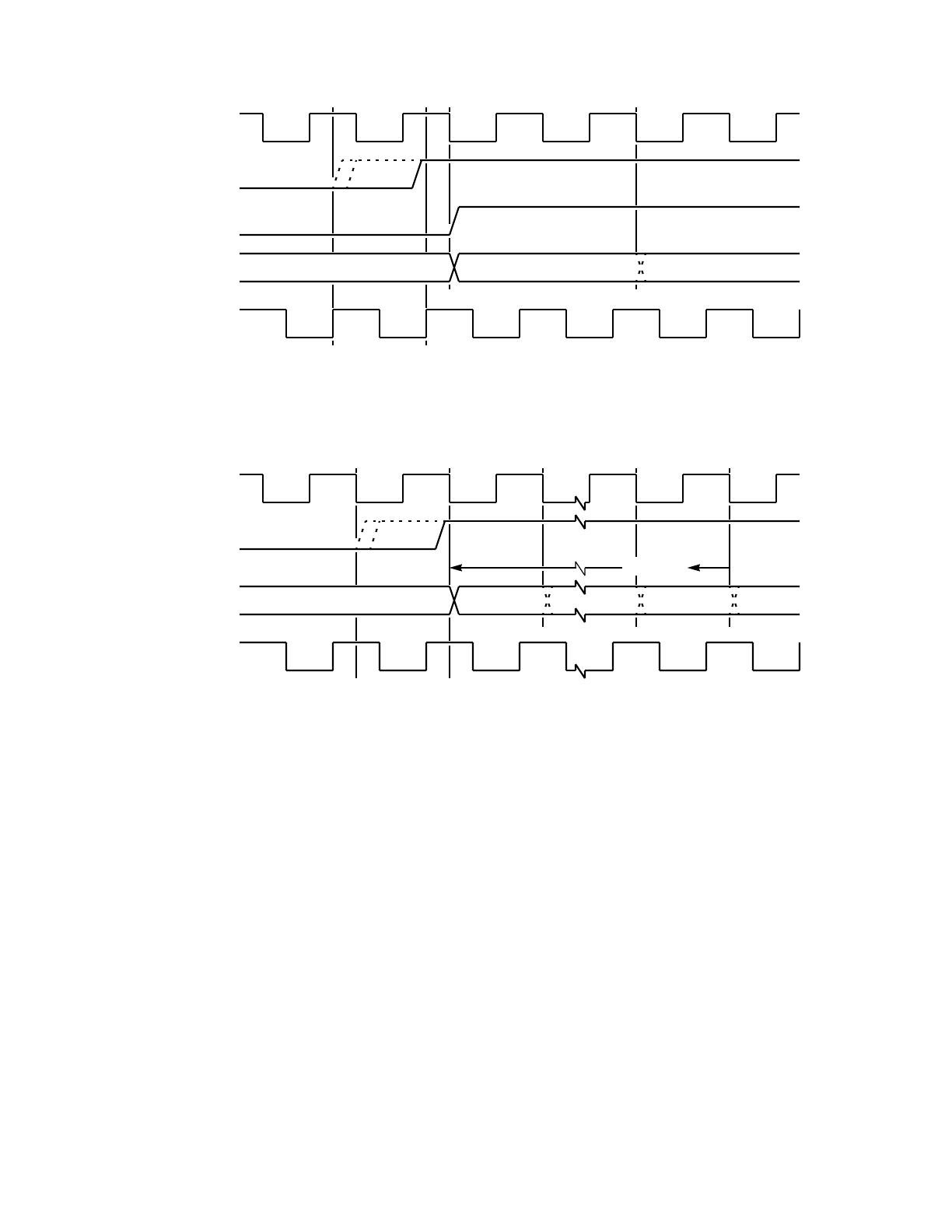
MOTOROLA PULSE ACCUMULATOR M68HC11
11-10 REFERENCE MANUAL
Figure 11-4 PAI Pin Edge-Detection Timing
Figure 11-5 Pin Enable vs. Counting (Gated Accumulation Mode)
In gated time accumulation mode, an internal, free-running E divided by 64 clock
drives the PACNT whenever the PAI pin is at its chosen active level. Figure 11-5
shows the timing relationship between the counter enable signal at the PAI pin [1] and
the start of counting. In general, the signal at the PAI pin is asynchronous to the free-
running E divided by 64 clock; thus, there would be an uncertainty about the delay be-
tween the active level at the PAI pin and the first increment of the PACNT. The first
increment could come as early as [2], as late as [5], or at any PH2 falling edge between
([3], [4], etc.).
Knowing the relationship between software and the free-running E divided by 64 clock
is not normally useful, but it is theoretically possible to determine this relationship.
From Figure 10-3 and the prescale control bit values (PR[1:0]), it can be determined
where the E divided by 64 clock is tapped off the main timer. Software can then read
the low-order half of the 16-bit main timer counter to see when the next edge will ap-
pear at the tap point. Because this procedure can be involved, it is not worth pursuing
unless there is a very good reason.
PH2
PAIF
E
PACNT COUNT N+1N
PAI PIN [1]
[2]
[3]
PH2
E
PACNT COUNT
PAI PIN [1]
[2] [3] [4] [5]
63 CYCLES
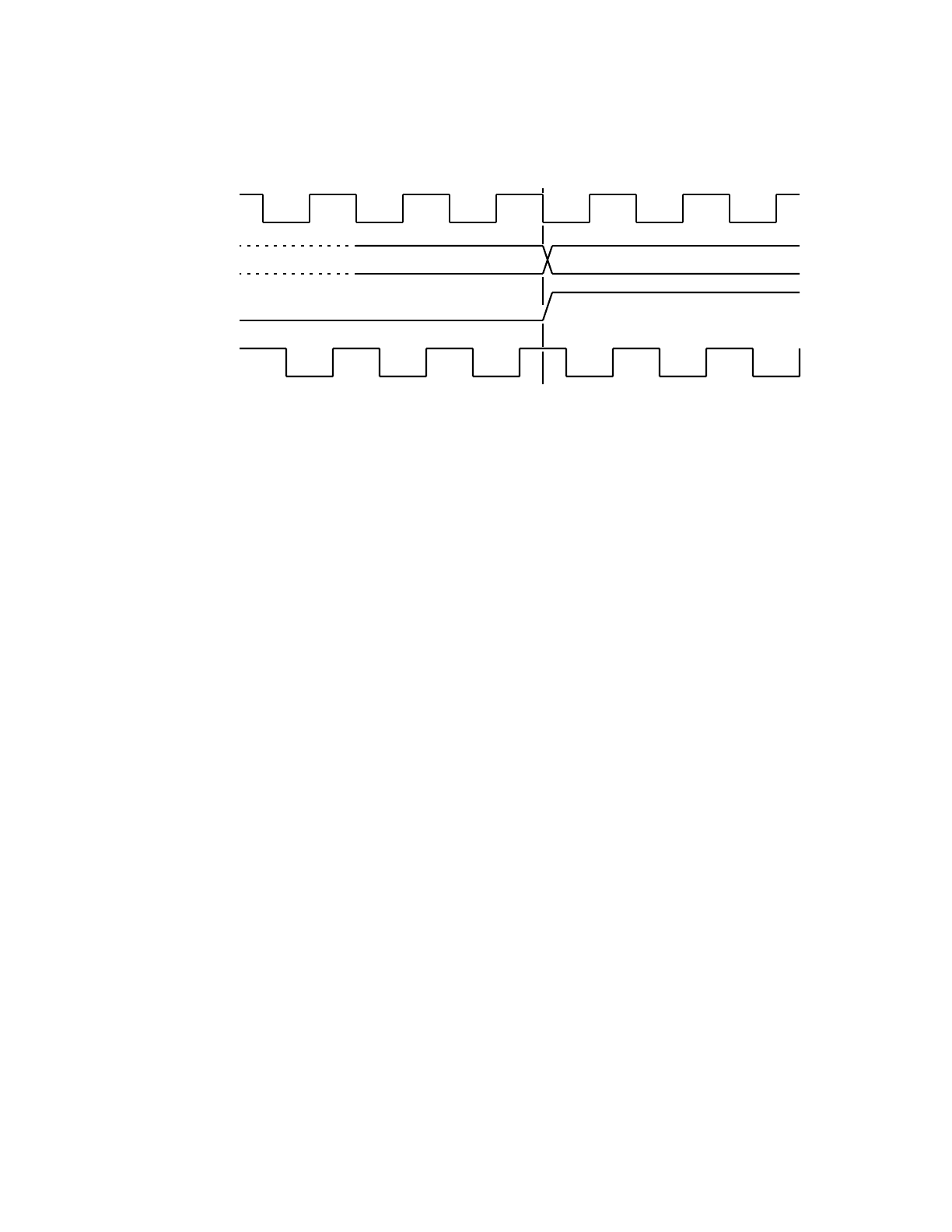
M68HC11 PULSE ACCUMULATOR MOTOROLA
REFERENCE MANUAL 11-11
Figure 11-6 shows timing details for a pulse accumulator counter overflow. At the PH2
falling edge where the PACNT count changes from $FF to $00 [1], the PAOVF bit also
is set [2].
Figure 11-6 Timing Details for Pulse Accumulator Counter Overflow
Reading or writing to the PACNT occurs in a portion of the PH2 cycle that eliminates
conflicts between accesses to PACNT and counting. (a) shows the detailed timing for
a read of PACNT; (b) shows a write. The address and data buses shown in are the
internal buses that have different timing than the external buses.
PH2
E
PACNT COUNT
PAOVF
[1]
[2]
$00$FF
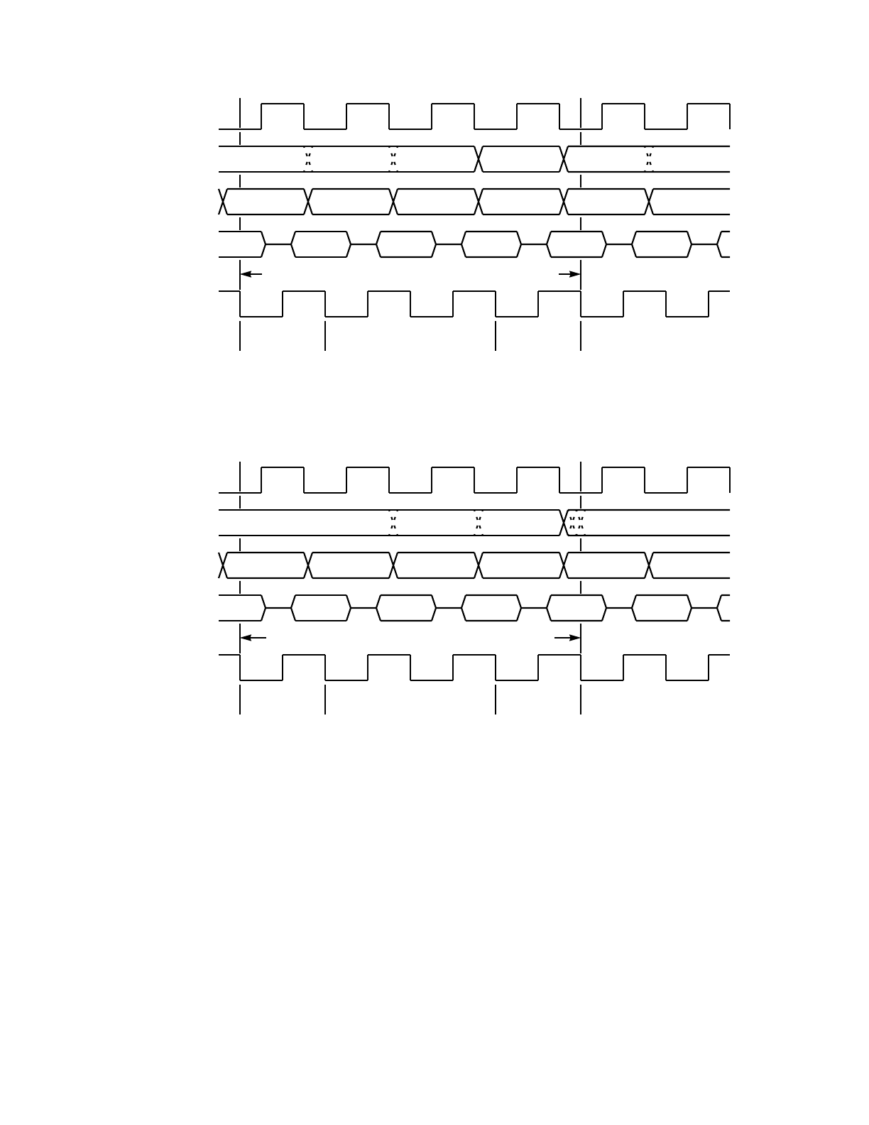
MOTOROLA PULSE ACCUMULATOR M68HC11
11-12 REFERENCE MANUAL
(a) PACNT Read
(b) PACNT Write
Figure 11-7 PACNT Read and Write
PH2
ADDRESS BUS
(INTERNAL)
E
PACNT COUNT
LDAA PACNT READ PULSE ACCUMULATOR COUNT (EXTENDED)
NN
OPCODE ADDR OPERAND (LO)OPERAND (HI) NEXT OPCODE
DATA BUS
(INTERNAL) NN$0E$10OPCODE
$1027 PACNT
FETCH OPCODE FETCH 16-BIT OPERAND ADDRESS READ PACNT
PH2
ADDRESS BUS
(INTERNAL)
E
PACNT COUNT
STAA PACNT WRITE TO PULSE ACCUMULATOR (EXTENDED)
NN
OPCODE ADDR OPERAND (LO)OPERAND (HI) NEXT OPCODE
DATA BUS
(INTERNAL) NN$27$10OPCODE
$1027 PACNT
FETCH OPCODE FETCH 16-BIT OPERAND ADDRESS WRITE PACNT
OLD COUNT

M68HC11 ANALOG-TO-DIGITAL CONVERTER SYSTEM MOTOROLA
REFERENCE MANUAL 12-1
SECTION 12
ANALOG-TO-DIGITAL CONVERTER SYSTEM
The MC68HC11A8 analog-to-digital (A/D) converter system uses an all-capacitive
charge-redistribution technique for conversions. The A/D system is an 8-channel, 8-
bit, successive approximation converter with ±1/2 least significant bit (LSB) accuracy
over the complete operating temperature range. Because of the charge-redistribution
technique, no external sample and hold circuits are required.
This section first discusses the charge-redistribution technique, which is useful in un-
derstanding subtle details concerning the application of the MC68HC11A8 A/D sys-
tem. The second part of this section includes a detailed description of the
MC68HC11A8 A/D system and features. The section concludes with a discussion of
how external circuitry can influence A/D accuracy.
12.1 Charge-Redistribution A/D
Figure 12-1 shows a simplified circuit to perform a 4-bit, successive-approximation A/
D conversion using charge redistribution. The actual circuit used in the MC68HC11A8
includes several additions to this simple circuit to improve quality and simplify manu-
facturing. After an initial introduction to the charge-redistribution technique, some of
these additions are discussed. Since the capacitive charge redistribution technique
depends upon capacitance ratios rather than absolute capacitance values, the capac-
itors in Figure 12-1 are marked in units.
During the sample time (Figure 12-1(a)), the top plate of all capacitors is switched to
VL(0.0 V), and the bottom plates are connected to the unknown analog input, VX. Us-
ing the simple relationship QS equals CV, the total charge may be calculated by
QS = 16(VX – VL)
Unless otherwise stated, it is assumed VL equals 0.0 V; therefore,
QS= 16 VX
Next, the circuit is changed to the hold state by logically controlled analog switches
(Figure 12-1(b)). In this state, the top plates are disconnected from VL, and the bottom
plates are switched from VX to VL. The charge is now written as
QH = (VL – Vi) 16
Since VL= 0
QH = – 16 Vi
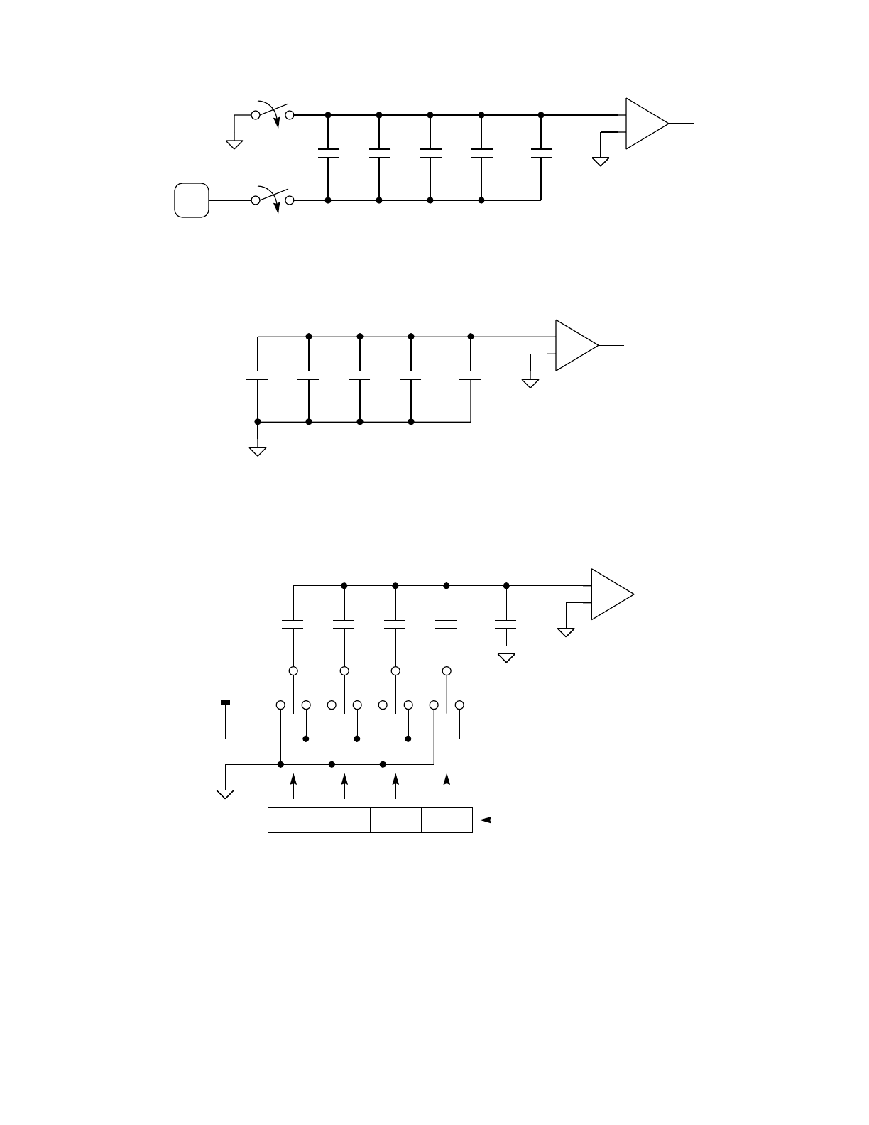
MOTOROLA ANALOG-TO-DIGITAL CONVERTER SYSTEM M68HC11
12-2 REFERENCE MANUAL
(a) Sample Mode
(b) Hold Mode
(c) Approximation Mode
Figure 12-1 Basic Charge-Redistribution A/D
Since charge is conserved, QS equals QH; therefore,
VX
+
–
Vi
1248 1
VL
VL
+
–
VL
Vi
1248 1
VL
+
–
VH
VL
Vi
MSB
1
10
LSB
SUCCESSIVE-APPROXIMATION REGISTER
(SAR)
101010
248 1
VL
VL
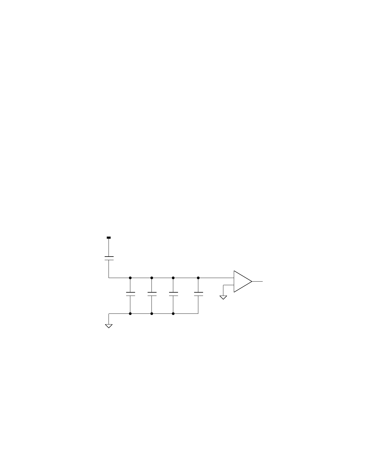
M68HC11 ANALOG-TO-DIGITAL CONVERTER SYSTEM MOTOROLA
REFERENCE MANUAL 12-3
16 VX = –16 Vi
VX = –Vi
Vi = –VX
which is the initial voltage at the input of the comparator.
Finally, in the conversion portion of the A/D process, each capacitor, beginning with
the largest one, which corresponds to the most significant bit (MSB) of the digital re-
sult, is switched from VL(0.0 V) to VH. The output of the comparator, after each ca-
pacitor is switched, determines whether the bottom plate of that capacitor will remain
at VH or be returned to VL before the next capacitor is switched.
To understand how the process works, a conversion sequence is presented for an an-
alog input, (VX equals 21/32 (VH).
During the sample time, the capacitors attain a total charge
QS = 16 VX = (16) 21/32 (VH) = 21/2 VH
During hold, the minus input to the comparator (Vi) goes to –VX or –21/32 VH.
Next, the eight-unit capacitor is switched from VLto VHresulting in the following circuit:
The charge is written as follows:
Q = 8 (VH – Vi) + 8 (VL – Vi)
but VL = 0; thus,
Q = 8 VH – 8 Vi – 8 Vi
Q = 8 VH – 16 Vi
By charge conservation, this charge is set equal to the original charge obtained during
VH
+
–
VL
124
8
1
VL
Vi
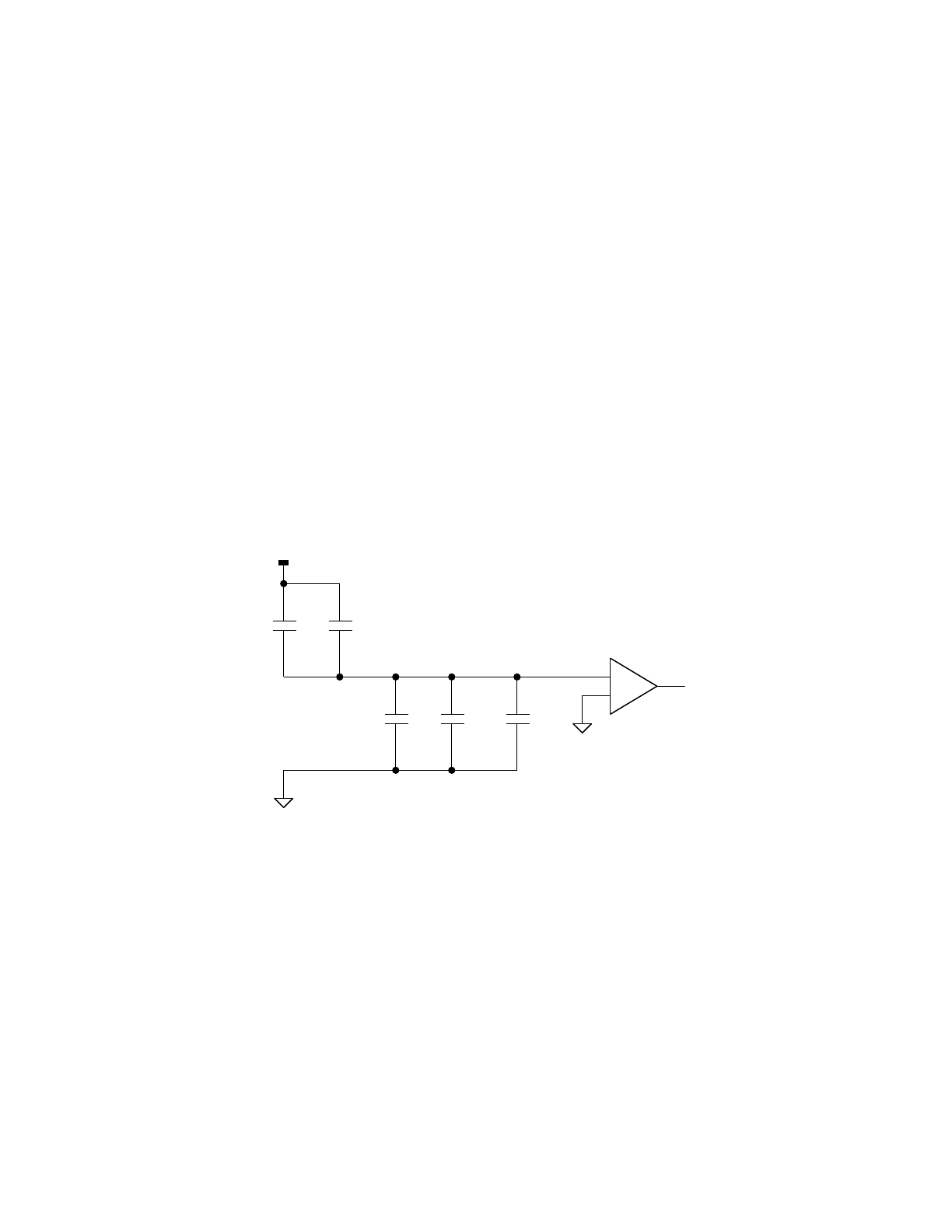
MOTOROLA ANALOG-TO-DIGITAL CONVERTER SYSTEM M68HC11
12-4 REFERENCE MANUAL
the sample time:
21/2 VH = 8 VH – 16 Vi
Solving for Vi yields the following results:
16 Vi = 8 VH – 21/2 VH
Vi = 1/2 VH – 21/32 VH
Vi = – 5/32 VH
which is negative.
Since the output of the comparator is a logic one, the eight-unit capacitor remains con-
nected to VHfor the next step. Also, bit 3 of the successive-approximation register
(SAR) is set to a logic one. After the conversion sequence, the SAR contains the digital
equivalent of the original analog input.
Next, the four-unit capacitor will be switched from VLto VHresulting in the following
circuit:
The charge is written as follows:
Q = 8(VH – Vi) + 4(VH – Vi) – 4 Vi
Q = 8 VH – 8 Vi + 4 VH – 4 Vi – 4 Vi
Q = 12 VH – 16 Vi
By charge conservation, this charge is set equal to the original charge:
21/2 VH = 12 VH – 16 Vi
Solving for Vi yields the following results:
VH
+
–
VL
12
48
1
VL
Vi
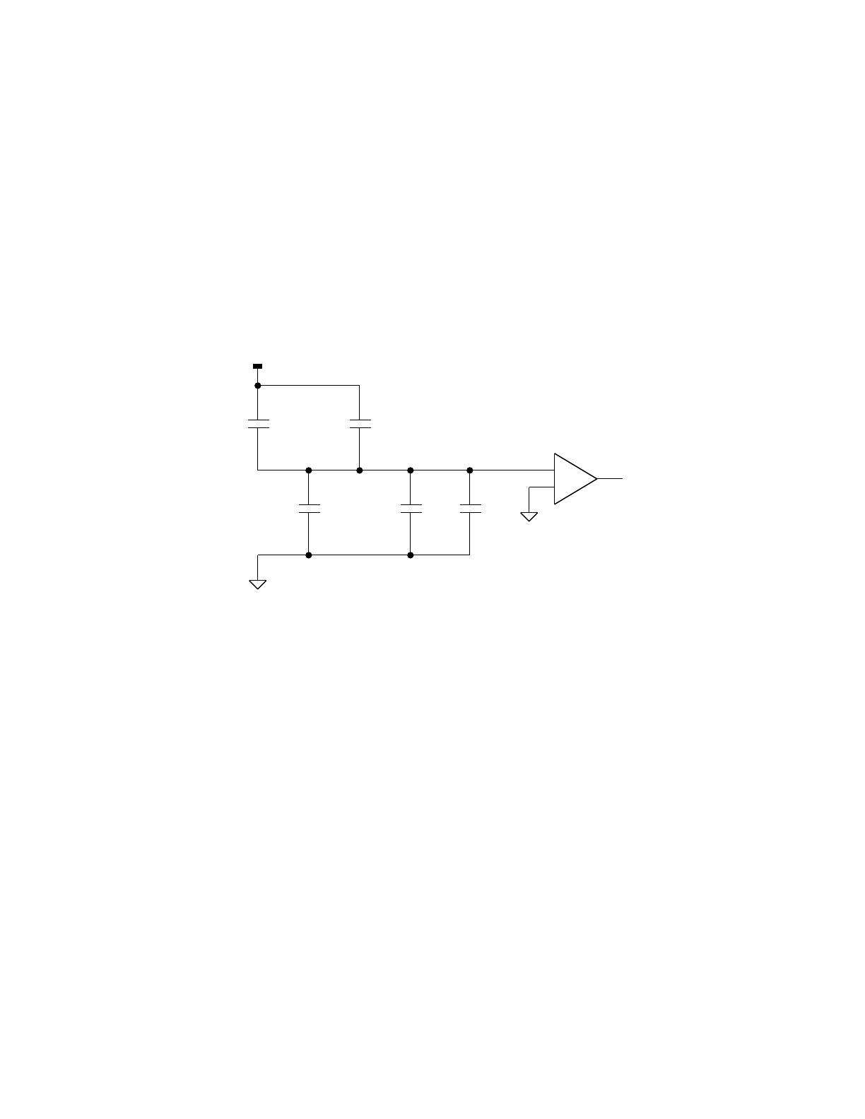
M68HC11 ANALOG-TO-DIGITAL CONVERTER SYSTEM MOTOROLA
REFERENCE MANUAL 12-5
16 Vi = 12 VH – 21/2 VH
16 Vi = 3/2 VH
Vi = 3/32 VH
which is positive.
The output of the comparator is a logic zero; therefore, the four-unit capacitor returns
to VL before proceeding to the next step. Also, bit 2 of the SAR is cleared to zero.
Next, the two-unit capacitor will be switched from VLto VHresulting in the following
circuit:
The charge is written as follows:
Q = 8(VH – Vi) + 2(VH – Vi) – 6 Vi
Q = 8 VH – 8 Vi + 2 VH – 2 Vi – 6 Vi
Q = 10 VH – 16 Vi
Setting this charge equal to the original charge by charge conversion yields the follow-
ing results:
21/2 VH = 10 VH – 16 Vi
16 Vi = 10 VH – 21/2 VH
16 Vi = – 1/2 VH
Vi = – 1/32 VH
which is negative.
Since the output of the comparator is now a logic one, the two-unit capacitor remains
VH
+
–
VL
1
2
4
8
1
VL
Vi
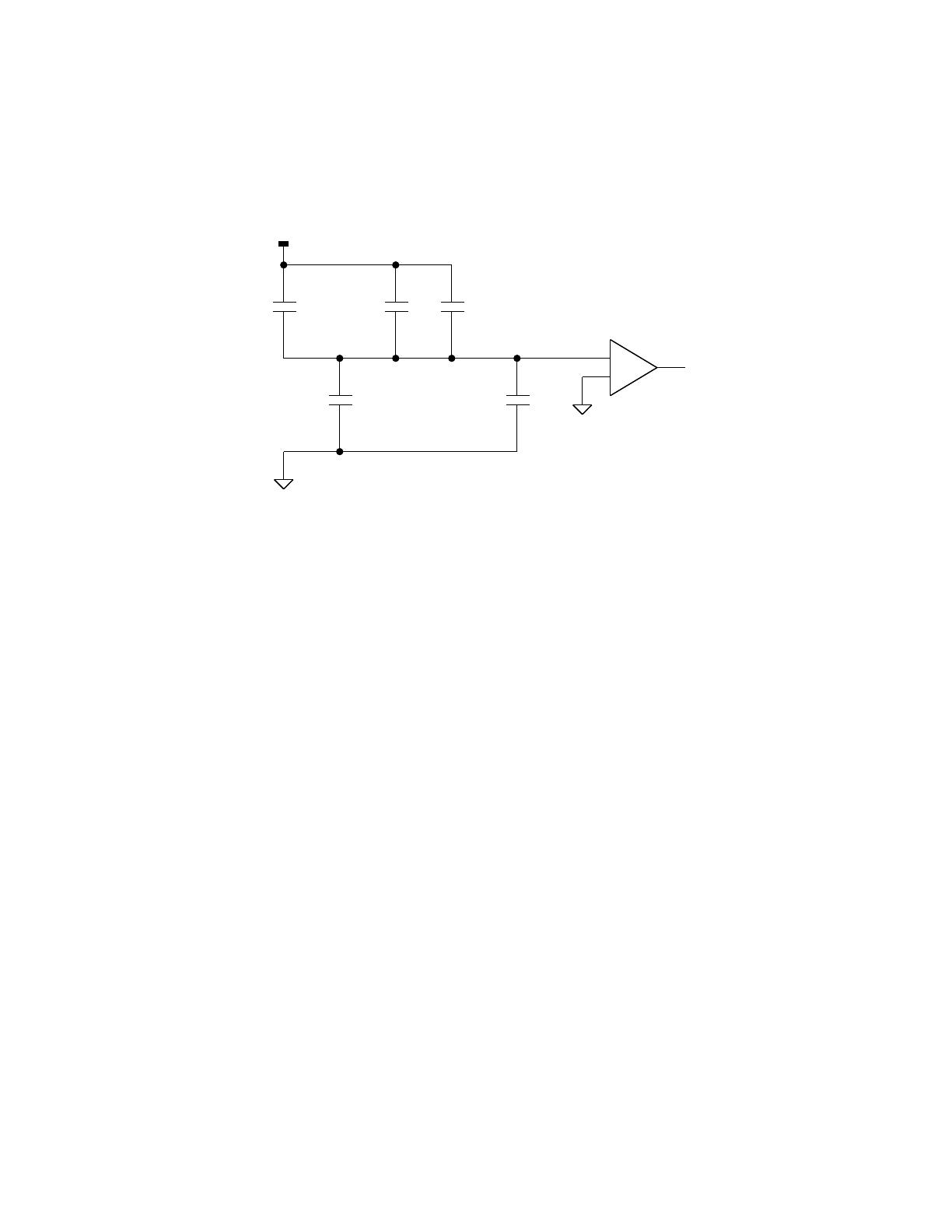
MOTOROLA ANALOG-TO-DIGITAL CONVERTER SYSTEM M68HC11
12-6 REFERENCE MANUAL
connected to VH for the next step, and bit 1 of the SAR is set to one.
As the last step in the conversion sequence, the one-unit capacitor will be switched fro
VLto VH. The second one-unit capacitor remains connected to VLthroughout the con-
version sequence. The following circuit is for the last conversion step:
The charge is now written as follows:
Q = 8(VH – Vi) + 2(VH – Vi) + 1 (VH – Vi) – 5 Vi
Q = 8 VH + 2 VH + 1 VH – 8 Vi – 2 Vi – 1 Vi – 5 Vi
Q = 11 VH– 16Vi
Charge conservation yields the following results:
21/2 VH = 11 VH – 16 Vi
16 Vi = 11 VH – 21/2 VH
16 Vi = 1/2 VH
Vi = 1/32 VH
which is positive.
Since the output of the comparator is now a logic zero, the LSB of the SAR is cleared
to zero. Because the conversion is complete, it is not necessary to switch the one-unit
capacitor back to VL. The digital result of this example conversion is 10102.
In the previous example, an analog input voltage of 21/32 VHyields a digital result of
10102or 10/16 VH. An error occurred even though ideal components and conditions
were assumed. A closer look at an even simpler 2-bit A/D explains the reason. If the
second one-unit capacitor is omitted, the following circuit results:
VH
+
–
VL
12
4
8
1
VL
Vi
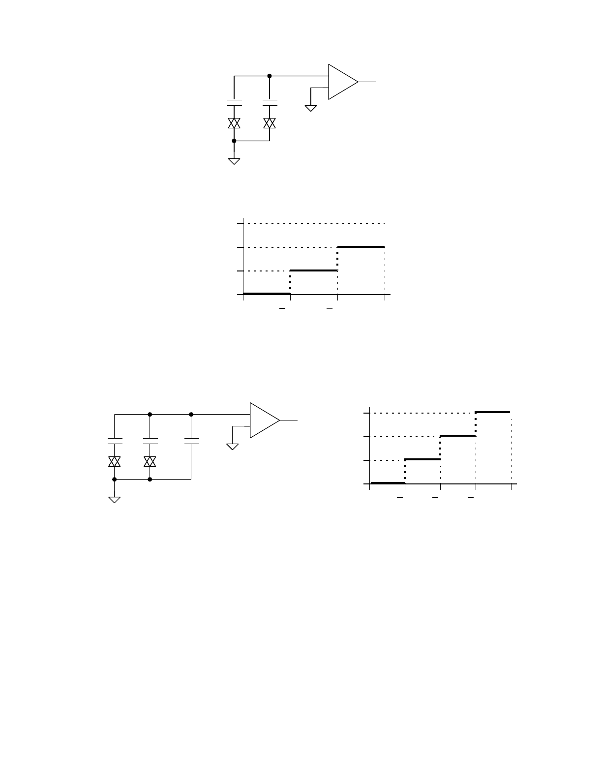
M68HC11 ANALOG-TO-DIGITAL CONVERTER SYSTEM MOTOROLA
REFERENCE MANUAL 12-7
The transfer characteristic of the circuit is as follows:
Without the extra one-unit capacitor, each unit of capacitance corresponds to one-third
the total rather than corresponding to the desired one-fourth. When the second one-
unit capacitor is added, the following circuit and transfer characteristics result:
An analog input of 1/4 VHproduces a digital result of 012or 1/4 VH, but an analog input
of 1/8 VHyields a digital result of 002or 0.0 V, which is in error by 1/8 VHor 1/2 LSB.
This quantization error is an unavoidable consequence of any A/D converter. This par-
ticular 2-bit A/D has a quantization error of –0/+1 LSB. A more desirable specification
is ±1/2 LSB quantization error, as is the case on the MC68HC11A8. Quantization error
is always a total of 1 LSB, and many manufacturers do not include this error in speci-
fications of A/D accuracy.
In an all-capacitive charge-redistribution converter, a simple method exists for shifting
the transfer characteristic down by 1/2 LSB to center the quantization error. A half-unit
capacitor is connected to VHduring the sample time and is switched to VLfor the re-
mainder of the conversion sequence. Figure 12-2 demonstrates how this technique is
applied to the previously described 2-bit converter.
+
–
VL
12
VL
VHVH
VH
VL
11
10
01
00
ANALOG INPUT
BINARY RESULT
1
32
3
+
–
VL
12
VL
1
VHVH
VL
11
10
01
00
ANALOG INPUT
BINARY RESULT
3
4
VH
1
2
VH
1
4

MOTOROLA ANALOG-TO-DIGITAL CONVERTER SYSTEM M68HC11
12-8 REFERENCE MANUAL
The charge obtained during the sample time is
QS = 4(VX – VL) + 1/2(VH – VL)
Assuming VL = 0 simplifies the equation to
QS = 4 VX+ 1/2 VH
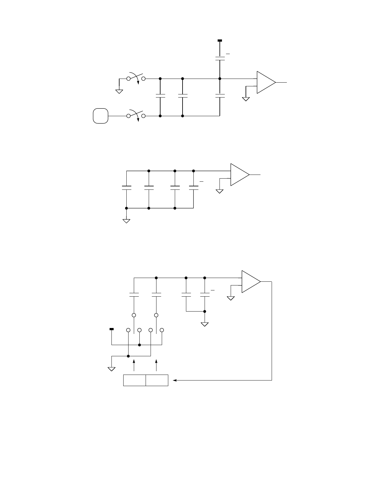
M68HC11 ANALOG-TO-DIGITAL CONVERTER SYSTEM MOTOROLA
REFERENCE MANUAL 12-9
(a) Sample Mode
(b) Hold Mode
(c) Approximation Mode
Figure 12-2 Charge-Redistribution A/D with ± 1/2 LSB Quantization Error
VX
+
–
Vi
12 1
VL
VL
1
2
+
–
VL
Vi
12
VL
1
2
1
+
–
VH
VL
Vi
BIT 1
1
BIT 0
SAR
1010
2 1
VL
VL
1
2
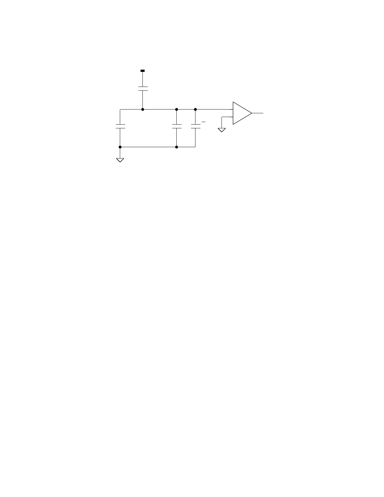
MOTOROLA ANALOG-TO-DIGITAL CONVERTER SYSTEM M68HC11
12-10 REFERENCE MANUAL
The effect of the half-unit capacitor becomes apparent when Viis calculated for the
circuit corresponding to a digital result of 012. The equivalent circuit is
The charge is now written as follows:
Q = 1 (VH – Vi) – 3-1/2 Vi
Q = VH – 4-1/2 Vi
Charge conservation yields the following results:
4 VX + 1/2 VH = VH – 4-1/2 Vi
4-1/2 Vi = VH – 1/2 VH – 4 VX
4-1/2 Vi = 1/2 VH – 4 VX
9 Vi= 1 VH– 8 VX
9/8 Vi = 1/8 VH – VX
The comparator only outputs a logic one when Viis less than zero, which is when VX
is greater than 1/8 VH.
Next, Viis calculated for the circuit corresponding to a digital result of 102. The equiv-
alent circuit is as follows:
+
–
Vi
1
2 1
VL
VL
VH
1
2
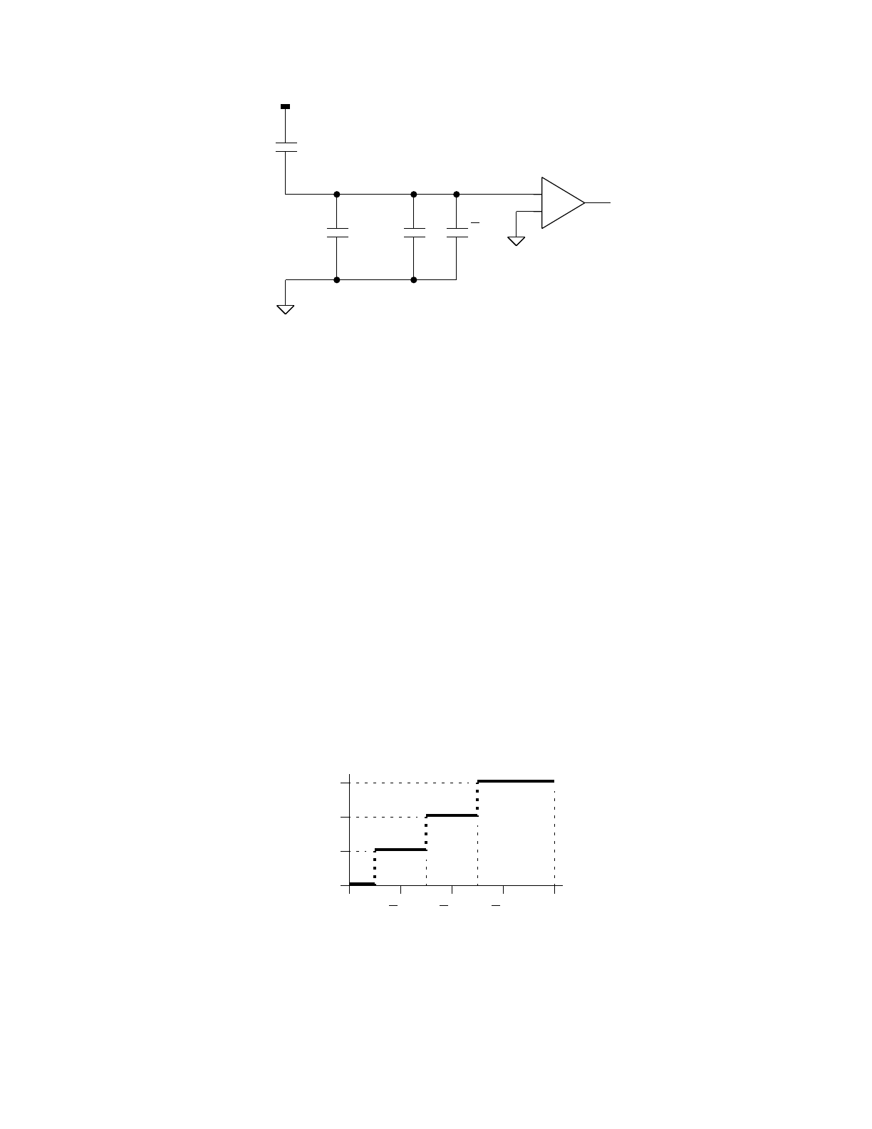
M68HC11 ANALOG-TO-DIGITAL CONVERTER SYSTEM MOTOROLA
REFERENCE MANUAL 12-11
The charge is written as follows:
Q = 2(VH – Vi) – 2-1/2 Vi
Q = 2 VH – 4-1/2 Vi
Change conservation yields the following results:
4 VX + 1/2 VH = 2 VH – 4-1/2 Vi
4-1/2 Vi = 2 VH – 1/2 VH – 4 VX
4-1/2 Vi = 3/2 VH – 4 VX
9 Vi = 3 VH – 8 VX
9/8 Vi = 3/8 VH – VX
The comparator only outputs a logic one when Viis less than zero, which is when VX
is greater than 3/8 VH. The complete transfer characteristic for the 2-bit A/D with the
new half-unit capacitor is
The user should note that there is no 2-bit digital code for 4/4 VH (full scale).
+
–
Vi
1
2
1
VL
VL
VH
1
2
VHVH
VL
11
10
01
00
ANALOG INPUT
BINARY RESULT
3
4
VH
1
2
VH
1
4
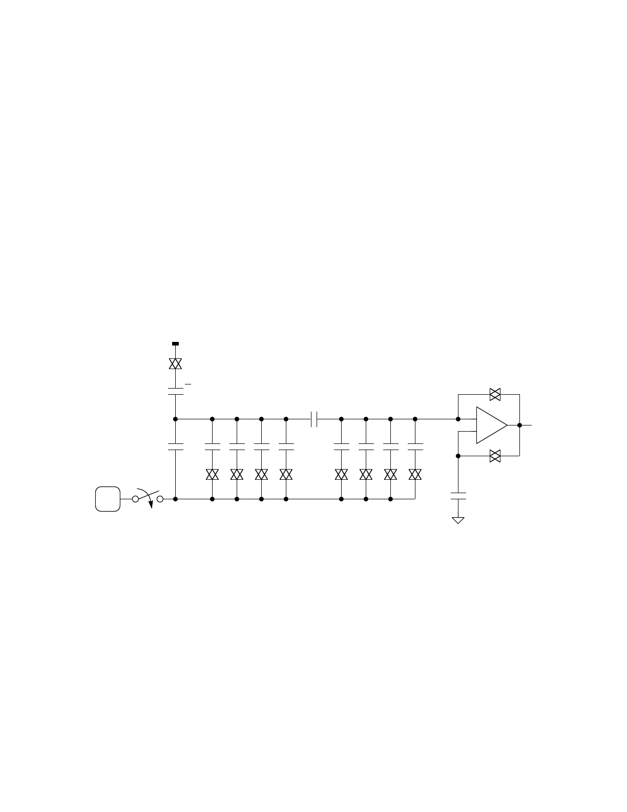
MOTOROLA ANALOG-TO-DIGITAL CONVERTER SYSTEM M68HC11
12-12 REFERENCE MANUAL
12.2 A/D Converter Implementation on MC68HC11A8
The A/D converter in the MC68HC11A8 is composed of a single successive-approxi-
mation charge-redistribution A/D converter and digital control circuitry. The analog
section is somewhat more complex than the circuits previously described but identical
charge-redistribution principles are used. The digital section consists of the logic that
makes the A/D work as a system with the rest of the microcontroller unit (MCU).
12.2.1 MC68HC11A8 Successive-Approximation A/D Converter
A discussion of the actual converter in the MC68HC11A8 is presented in the following
paragraphs. Figure 12-3 shows the successive-approximation converter of the
MC68HC11A8 A/D in sample mode.
Unlike earlier examples, the weighted capacitor array has a series capacitor (CS) sep-
arating the low-order half of the array from the high-order half. This capacitor effective-
ly divides the value of the low-order capacitors to the left by 16, which simplifies the
layout of the weighted capacitor array and assures better matching of capacitance siz-
es.
Figure 12-3 MC68HC11A8 A/D in Sample Mode
Except the half-unit and 1.1-unit elements, all capacitors are composed of connected
groups of one-unit capacitors, which minimizes errors caused by sizing and process-
ing. In the MC68HC11A8, these capacitors consist of polysilicon plates separated by
an inter-level oxide; the lower plates are isolated from the substrate by a second layer
of oxide. The capacitance of this structure is not subject to variation due to voltages
on the plates relative to the substrate.
In the MC68HC11A8 A/D, both inputs and the output of the comparator are shorted
together during the sample time, which causes all three points to stabilize at the trip
voltage of the comparator; thus, comparator offsets are effectively cancelled out of the
VX
+
–
Vi
211
VL
VH
1
2
8421 84
1.1
CS
16
VTRIP

M68HC11 ANALOG-TO-DIGITAL CONVERTER SYSTEM MOTOROLA
REFERENCE MANUAL 12-13
calculations. After the sample period, the shorting paths are disconnected, and the
conversion sequence proceeds as in the earlier examples. The 16-unit capacitor from
the plus input of the comparator to VLis not critical in terms of size because it is only
used to hold the plus input at VTRIP during the short conversion time.
12.2.2 A/D Charge Pump and Resistor-Capacitor (RC) Oscillator
A charge pump on the chip develops about 7 or 8 V, and this high voltage is used to
drive the gates of the analog switches in the input multiplexer and capacitor array. This
high gate voltage assures low source to drain impedance for analog signals up to and
including VDD. In fact, VRH can be somewhat higher than VDD (approximately 6 V), and
the converter will still yield good ratiometric results.
The A/D charge pump is disabled coming out of reset and is turned on by setting the
A/D power-up (ADPU) control bit in the OPTION control register before the A/D system
can be used. A delay is required after turning on ADPU to allow the charge pump and
comparator circuits to stabilize before using the converter system.
The charge-redistribution A/D process is a dynamic process in that the charge on the
capacitor array will eventually leak off. This capacitor array is part of an internal digital-
to-analog converter (DAC), which means the conversion process must be completed
within a reasonable time after the sample time ends. The other circuitry on the MCU
is static to allow very low clock frequencies, thus saving power. At bus frequencies (E
clock) below 750 kHz, the E clock should not normally be used as the A/D conversion
clock because there is a risk of error due to charge leakage at temperature extremes.
Laboratory characterization has indicated good performance at E-clock rates as low
as 10 kHz, but the specification has been guard banded against process variations.
An on-chip RC oscillator provides an alternate clocking source for the A/D system
when the E clock is running too slow to assure good conversions. This clock source is
selected by writing a one to the clock select (CSEL) control bit in the OPTION control
register. The A/D clock (E clock or RC oscillator depending on CSEL) drives the SAR
sequencer and the A/D charge pump. Some delay may be required after switching
clock sources, depending on their frequencies. The RC oscillator frequency varies with
processing but is typically about 2 MHz.
When the E clock is being used as the A/D clock source, the conversion sequence is
inherently synchronized to the main MCU clocks. Using the E clock has two advantag-
es over using the RC oscillator, which is asynchronous to system clocks. First, the
comparator output is sampled at relatively quiet times in the system clock cycle, thus
reducing the effects of internal MCU noise. When the RC oscillator is being used, there
is more error attributable to internal system clock noise. Second, result-register up-
dates automatically occur during a portion of the system clock cycle where reads do
not occur; thus, an update cannot interfere with a read. When the RC oscillator is used,
there is no conflict between updates and reads, but there is an additional synchroni-
zation delay imposed at the end of each channel conversion to allow for synchroniza-
tion to the system E clock.
The following illustration shows the OPTION control register for reference since the

MOTOROLA ANALOG-TO-DIGITAL CONVERTER SYSTEM M68HC11
12-14 REFERENCE MANUAL
ADPU and CSEL control bits affect the A/D converter system.
The CSEL control bit also selects an alternate clock source for the on-chip EEPROM
charge pump. This charge pump is separate from the A/D charge pump, but both
pumps are selected with the CSEL control bit. In the case of the A/D charge pump,
CSEL needs to be one when the E clock is too slow to assure that the successive-ap-
proximation sequence will finish before any significant charge loss. In the case of the
EEPROM, the efficiency of the charge pump is at issue. More details on EEPROM
charge-pump efficiency are presented in SECTION 4 ON-CHIP MEMORY. When the
E clock is at or above 2 MHz, CSEL should always be zero; when the E clock is below
750 kHz, CSEL should almost always be one.
At E-clock frequencies between 750 kHz and 2 MHz, CSEL should be set to one for
EEPROM programming and erase operations so the EEPROM charge pump works
more efficiently; however, CSEL should be set to zero for A/D conversions to assure
highest A/D accuracy by reducing the effects of on-chip noise.
In most applications, switching CSEL on and off is not necessary. Instead, a trade-off
can usually be made on the basis of application requirements. For example, the addi-
tional A/D error attributable to internal noise when CSEL equals one is on the order of
±1/2 LSB, which is acceptable in many applications.
12.2.3 MC68HC11A8 A/D System Control Logic
The A/D system on the MC68HC11A8 consists of a single successive-approximation
A/D converter, an input multiplexer to select one of 16 channels (including eight chan-
nels associated with pins on the MCU), and sophisticated control circuitry to configure
and control conversion activities. Four separate result registers are included with con-
trol logic that implements automatic conversion sequences on a selected channel four
times or on four channels (once each). Conversion sequences are configured to re-
peat continuously or to stop after one set of four conversions. An on-chip RC oscillator
is selected to allow normal operation of the A/D when very low MCU clock frequencies
are being used.
Figure 12-4 shows the timing for a sequence of four A/D conversions; the system E
clock is being used as the conversion clock, which is the normal case. The A/D con-
verter is dynamic in that the charge attained during the sample period will eventually
leak off the DAC capacitors. If the system E clock is slower than 750 kHz, an on-chip
RC oscillator should be selected as the A/D conversion clock source. The RC clock
source is selected by setting the CSEL control bit in the OPTION register. Since the
RC clock source is asynchronous to the MCU E clock, a synchronization delay is re-
quired at the end of each conversion in the sequence to prevent result-register up-
dates in the same part of the E-clock cycle where a read is taking place. A/D result
registers should not normally be used before the conversion complete flag (CCF) is
OPTION — System Configuration Options $1039
BIT 7 654321BIT 0
ADPU CSEL IRQE DLY CME CR1 CR0
RESET: 00010000
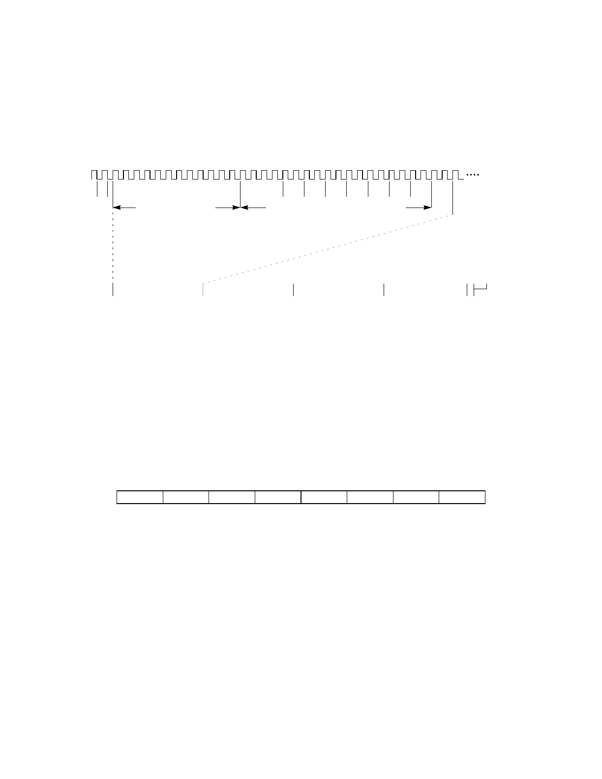
M68HC11 ANALOG-TO-DIGITAL CONVERTER SYSTEM MOTOROLA
REFERENCE MANUAL 12-15
set at the end of the fourth conversion in a sequence because of uncertainty in the ex-
act frequency of the on-chip RC oscillator and because of synchronization delays.
When the E clock is being used as the conversion clock, Figure 12-4 can be used to
determine the earliest availability of valid data in result registers 3–1. For example,
ADR1 has valid conversion results 34 E-clock cycles after the A/D control/status reg-
ister is written.
Figure 12-4 Timing Diagram for a Sequence of Four A/D Conversions
12.2.4 A/D Control/Status Register (ADCTL)
All bits in this register may be read or written except bit 7, which is a read-only status
indicator, and bit 6, which always reads zero. Bit 7 is cleared by reset, but the other
bits are not affected by reset. The following register and paragraphs describe the func-
tion of each bit.
CCF — Conversions Complete Flag
This read-only status indicator is set when all four A/D result registers contain valid
conversion results. Each time the ADCTL register is written, this bit is automatically
cleared, and a new conversion sequence is started immediately. In the continuous
scan modes, conversions continue in round-robin fashion, and the result registers are
updated with current data even though the CCF bit remains set.
NOTE
The user must write to the ADCTL register to initiate conversion oper-
ations. To abort a conversion operation in progress, write to the
ADCTL register, and a new conversion operation is initiated
immediately.
ADCTL — A/D Control/Status Register $1030
BIT 7 654321BIT 0
CCF — SCAN MULT CD CC CB CA
RESET: 0 0 UUUUUU
0 32 64 96 128 — E CYCLES
SAMPLE ANALOG INPUT SUCCESSIVE APPROXIMATION SEQUENCE
MSB
4
CYCLES
BIT 6
2
CYC
BIT 5
2
CYC
BIT 4
2
CYC
BIT 3
2
CYC
BIT 2
2
CYC
BIT 1
2
CYC
LSB
2
CYC
2
CYC
END
REPEAT SEQUENCE, SCAN = 1
SET CC FLAG
CONVERT FIRST
CHANNEL, UPDATE
ADR1
CONVERT SECOND
CHANNEL, UPDATE
ADR2
CONVERT THIRD
CHANNEL, UPDATE
ADR3
CONVERT FOURTH
CHANNEL, UPDATE
ADR4
12 E CYCLES
WRITE TO ADCTL
E CLOCK

MOTOROLA ANALOG-TO-DIGITAL CONVERTER SYSTEM M68HC11
12-16 REFERENCE MANUAL
Bit 6 — Not implemented; always reads zero.
SCAN — Continuous Scan Control
When this bit is zero, the four requested conversions are performed, once each, to fill
the four result registers. When this bit is one, conversions continue in a round-robin
fashion with the result registers being updated as new data becomes available.
MULT — Multiple-Channel/Single-Channel Control
When this bit is zero, the A/D system is configured to perform four consecutive con-
versions on the single channel specified by the four channel-select bits (CD:CA of the
ADCTL register). When this control bit is one, the A/D system is configured to perform
conversions on each channel in the group of four channels specified by the CD and
CC channel-select bits. In this multiple-channel mode, each channel is associated with
a specific result register.
CD, CC, CB, CA — Channel Selects
These four channel-select bits are used to specify the channel(s) to be operated on for
an A/D conversion operation. Table 12-1 shows the relationship between the CD-CA
bits and the channel(s) to be operated on. When a multiple-channel mode is selected
(MULT = 1), the CB and CA selects have no effect, and the group of four channels af-
fected are selected by CD and CC.
The last group of four analog channels is used during factory testing of the MCU. The
1/2 VRH channel is misleading in that there is no internal voltage divider actually divid-
ing the reference supply. Rather, a result of 1/2 VRH is artificially produced by special
Table 12-1 A/D Channel Assignments
CD CC CB CA Channel Signal Result in ADRx
if MULT = 1
0000 PE0 ADR1
0001 PE1 ADR2
0010 PE2 ADR3
0011 PE3 ADR4
0100 PE4* ADR1
0101 PE5* ADR2
0110 PE6* ADR3
0111 PE7* ADR4
1000Reserved ADR1
1001Reserved ADR2
1010Reserved ADR3
1011Reserved ADR4
1100 VH** ADR1
1101 VL** ADR2
1110 1/2 VH** ADR3
1111Reserved** ADR4
*Not available in 48-pin package versions.
**These channels intended for factory testing.
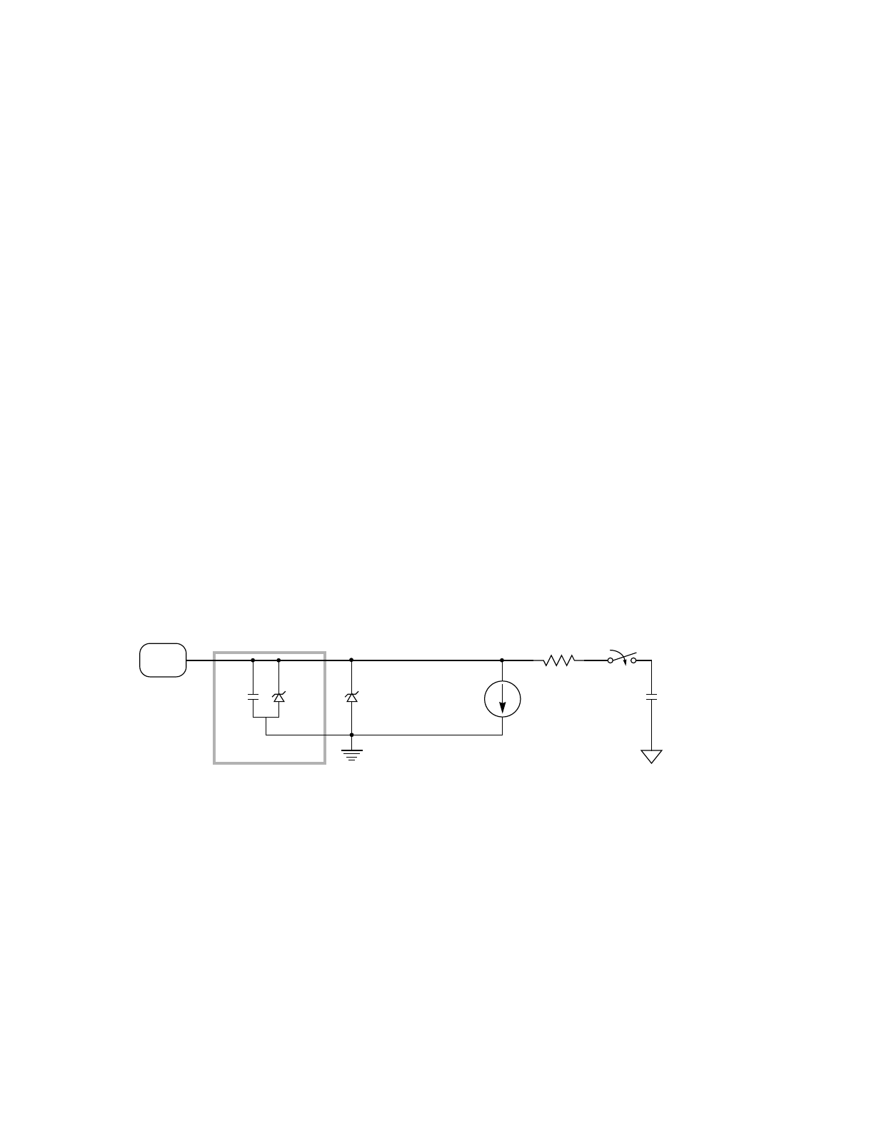
M68HC11 ANALOG-TO-DIGITAL CONVERTER SYSTEM MOTOROLA
REFERENCE MANUAL 12-17
control logic, which forces unusual connections of the DAC capacitors during sample
time. Thus, the charge attained will be identical to that obtained by sampling an analog
level of 1/2 VRH on one of the eight analog input pins.
12.2.5 A/D Result Registers (ADR[4:1])
The A/D result registers are read-only registers used to hold an 8-bit conversion result.
After all four result registers have been filled with valid data in a conversion sequence,
the CCF status bit is set to indicate the results are valid. New conversion results are
calculated in the A/D logic and are transferred into the result registers in a part of the
clock cycle where reads do not take place; therefore, no interference occurs between
software reads and result updates.
12.3 A/D Pin Connection Considerations
Since there are no P-channel devices directly connected to the A/D input or reference
pins, voltages above VDD do not pose a latchup threat. If an A/D input rises above the
threshold of the protection device, an input protection device avalanches, and current
into this device should be limited. Because of an inherent diode to VSS, A/D inputs
must not go below VSS, or the input can be permanently damaged. A series resistor of
1kΩwill prevent damage, but avoid a series resistor of more than 10 kΩbecause input
leakage acting through this impedance will degrade A/D accuracy. External clamping
diodes on A/D inputs should be avoided because the leakage through these devices
is greater than the input pin leakage current and could significantly degrade accuracy
if significant resistance exists in series with the analog source. Figure 12-5 shows a
model of an A/D input pin, which is useful in planning external circuitry and connec-
tions.
Figure 12-5 Electrical Model of an A/D Input Pin (Sample Mode)
Capacitors from A/D inputs to VRL help prevent errors due to system noise, but it is
important to size these capacitors properly for the way the A/D converter is being used
in a particular system. Factors affecting the size of these capacitors are as follows:
1. Source impedance of the analog signal
2. Rate of change of the analog signal
DIFFUSION/POLY
< 2 pF
COUPLER
400 nA
JUNCTION
LEAKAGE
+ ~20V
– ~0.7V
*
* THIS ANALOG SWITCH IS CLOSED ONLY DURING THE 12-CYCLE SAMPLE TIME.
VRL
INPUT
+ ~12V
– ~0.7V
PROTECTION
DEVICE
≤ 4 KΩ
DUMMY N-CHANNEL
OUTPUT DEVICE
ANALOG
INPUT
PIN
~ 20 pF DAC
CAPACITANCE

MOTOROLA ANALOG-TO-DIGITAL CONVERTER SYSTEM M68HC11
12-18 REFERENCE MANUAL
3. Electrical model of the A/D inputs
4. Frequency of A/D conversion requests to the particular channel
5. Analog level on the previously converted channel (in some cases)
The first three factors are straightforward, but the last two factors are subtle. Figure
12-4 and Figure 12-5 should be used in conjunction with the following discussion.
The maximum external source impedance of an analog signal is limited by the leakage
into the pin (see Figure 12-5). When VRH –V
RL = 5.12 V, 1 LSB corresponds to 20
mV of input voltage. The worst-case input leakage of 400 nA acting through 10 kΩof
external series resistance will result in about 0.2 LSBs of offset. Although the specifi-
cation states the maximum-allowable external series resistance is 10 kΩ, a higher
source impedance can be used, but it may cause additional errors in the results. The
leakage current arises from N-channel junction leakages that are worse at high tem-
peratures. Since only N-channel devices contribute to this current, it is unidirectional
toward VSS and will only cause errors, lowering A/D results below the expected value.
The minimum-desirable source impedance for an analog input signal should ensure
the current at the A/D pin never gets high enough to cause CMOS latchup. The HC-
MOS process used on the MC68HC11A8 is much more robust than older 14xxx-style
CMOS, but the current at a pin should still be limited to 25 mA or less. Although the
pins can withstand much more, 25 mA is considered a good design target. The source
impedance that meets this limitation will depend on the total system. For example,
suppose the worst-case scenario for a particular system results in an analog source
accidentally shorting to –12 V. The inherent internal diodes to VSS will clamp the volt-
age at the pin to about –0.7 V. This clamped voltage means a maximum current of 25
mA must cause 11.3 V to be dropped across a series-limiting resistance, which calcu-
lates to 452 Ω. However, some guard band should be allowed for tolerances on the
clamped voltage, the source voltages, the resistor, etc.
NOTE
Two of the most common A/D application errors have been either too
much source impedance, resulting in higher-than-expected errors, or
too little source impedance, resulting in permanent damage to A/D
inputs. The most common cause of damage to A/D inputs is a very
low source impedance to a negative voltage, which is more than 1 V
below VSS.
The rate of change of the analog input signal is important if an external low-pass filter
is used to increase noise immunity. If too large an RC time constant is chosen for the
external filter, meaningful transitions may be filtered out of analog signal source. An
external lowpass filter also introduces a delay between the analog source and the A/
D input pin. If the A/D system is used to locate a timing reference to a peak level on
an analog input signal, this delay must be considered. If the input to a channel changes
drastically between successive samples in a sequence of conversions, a charge-share
mechanism can affect the accuracy of the result as described in the following para-
graphs. This charge-share mechanism is normally only visible in multiple-channel,
continuous-scan conversion sequences where two adjacent channels are connected

M68HC11 ANALOG-TO-DIGITAL CONVERTER SYSTEM MOTOROLA
REFERENCE MANUAL 12-19
to grossly different analog levels.
A subtle aspect of Figure 12-5 is that the DAC capacitance is shared by all conver-
sions. This aspect results in the initial voltage on the DAC capacitance, just before a
sample period, being approximately equal to the voltage on the last channel convert-
ed. For individual conversions, this result usually does not produce any observable ef-
fect because the charge stored in the internal DAC capacitance is so small. Consider
what happens when a multiple-channel, continuous-scan conversion operation is oc-
curring (MULT and SCAN = 1). For an E-clock rate of 2 MHz, a particular channel is
sampled once every 64 µs. Each time, the initial voltage on the DAC capacitance just
before the sample is equal to the voltage on the previously sampled channel. Over
15,000 times a second a small amount of charge is removed from or added to the ex-
ternal capacitance on the pin. The charge is restored by charging or discharging
through the external source impedance. For some values of external R and C, the
charge added during the sample time cannot be fully bled off through the external RC
before the next sample time occurs. This problem causes a stair-step building of
charge in the external capacitance that builds until an equilibrium is reached, in which
the amount of charge added during a sample time is exactly offset by the charge bled
off during the period between samples. This condition is a secondary effect, which sel-
dom results in more than an LSB of error (even in the most extreme case). After study-
ing the mechanism, it should be fairly easy to avoid problems from this effect by careful
choice of the external R and C values, by avoiding channel assignments resulting in
grossly different levels on adjacent critical channels, and/or by avoiding the multiple-
channel, continuous-scan conversion modes when a high-frequency E clock is being
used.
Three types of cases must be considered, which result from the interaction of an ex-
ternal RC filter and the internal model of an A/D input pin. The method of determining
the error expected from a particular choice of external component values depends on
which of the three cases applies. Errors arise from leakage current acting through the
external series resistance or from system noise. If a very large external series imped-
ance is used, a problem can arise where the internal DAC capacitance cannot be prop-
erly charged within the 12-cycle sample time; however, errors due to simple leakage
through the external resistance usually do not allow using a large enough external re-
sistance to cause this effect. The following paragraphs describe the cases of interac-
tion of an external filter to the input model.
The first case arises when the external time constant is small compared to the length
of the 12-cycle sample period. In this case, all residual charge on the internal DAC ca-
pacitance is dissipated, and the pin settles at the expected voltage before the end of
the sample time. The problem with this case is that a filter with such a short time con-
stant provides very little filtering. In this case no errors result; thus, no calculations are
needed.
The second case arises when the external time constant is long compared to the sam-
ple period but is relatively short compared to the period between samples. In this case,
the residual charge on the internal DAC capacitance is redistributed to the external ca-
pacitance during the sample, but this charge is not dissipated through the external re-

MOTOROLA ANALOG-TO-DIGITAL CONVERTER SYSTEM M68HC11
12-20 REFERENCE MANUAL
sistance before the end of the sample time. This condition results in a small error in
the sample, but this charge is dissipated before the next sample of this channel. Thus,
no accumulated error occurs. In cases of this second type, the primary governing fac-
tor is the redistribution of the residual charge from the internal DAC capacitance. Usu-
ally, the external capacitance is so much larger than the internal DAC capacitance that
the voltage change due to charge redistribution reduces to the difference between the
previous channel voltage and the current channel voltage times the ratio of the internal
DAC capacitance to the external capacitance. Some of this charge is dissipated before
the end of the sample period by the external RC time constant. Figure 12-6 is a graph-
ic estimation of the amount of error resulting in such a case. Errors of this type are
present even in single-pass conversion sequences but rarely cause noticeable errors.
In Figure 12-6, the solid waveform [4] is the graphic estimation of the analog level at
an A/D input. This waveform results from the simultaneous operation of charge redis-
tribution of the residual charge on the internal DAC capacitance just before the sample
period began at to and from the dissipation of this charge through the external RC net-
work. Waveform [2] has a time constant, T80 ns, based on the model of an A/D input.
The peak level [1] is
(VA– VB) x (Ci÷(CX+ Ci))
where
VA= the analog level driving the previously sampled channel
VB = the level driving the currently sampled channel
Ci = the internal DAC capacitance
CX = the external capacitance
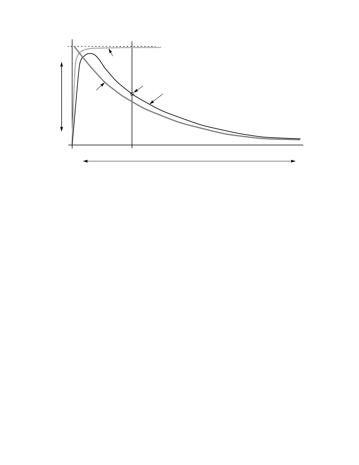
M68HC11 ANALOG-TO-DIGITAL CONVERTER SYSTEM MOTOROLA
REFERENCE MANUAL 12-21
Figure 12-6 Graphic Estimation of Analog Sample Level (Case 2)
Waveform [3] is the familiar RC exponential decay through the external network, and
it is assumed that the external capacitance is very large compared to the 20 pF DAC
capacitance. The time, t1, marks the end of the 12-cycle sample period, and level [5]
is the level that will be captured, held, and converted even though the pin voltage con-
tinues to decay through the external network.
The third case arises when the external time constant is very long compared to the
time between samples. In this case, the residual charge redistributed during the first
sample is not completely dissipated before the next sample; thus, there is an accumu-
lation of charge. This accumulation causes increasing errors on successive samples
until equilibrium is reached between the charge added during a sample and the charge
dissipated between samples. Errors caused by cases of this third type are often mis-
interpreted as leakage between adjacent channels. The magnitude of this type error
is estimated by developing equations for voltage change caused by charge added dur-
ing a sample time and voltage change caused by the action of the external RC be-
tween successive samples. These two equations are set equal to each other, and the
equilibrium voltage can then be resolved.
The voltage change during the sample is controlled by the ratio of the internal DAC
capacitance to the external capacitance (as in the previous case), but the external RC
is assumed to be so long that it produces no significant effect until after the sample
time ends. The voltage change between samples results from a simple RC exponen-
tial decay.
To illustrate the estimation of errors resulting from a case-three situation, consider this
example. The E-clock rate equals 2 MHz, VRH equals 5.12 V, VRL equals 0.0 V, chan-
nel one is connected to a 5.12-V analog level, and channel 2 is connected to a 0-V
[1]
[2]
[3] [4]
[5]
t1
t0
0.0 V
TIME
PIN VOLTAGE
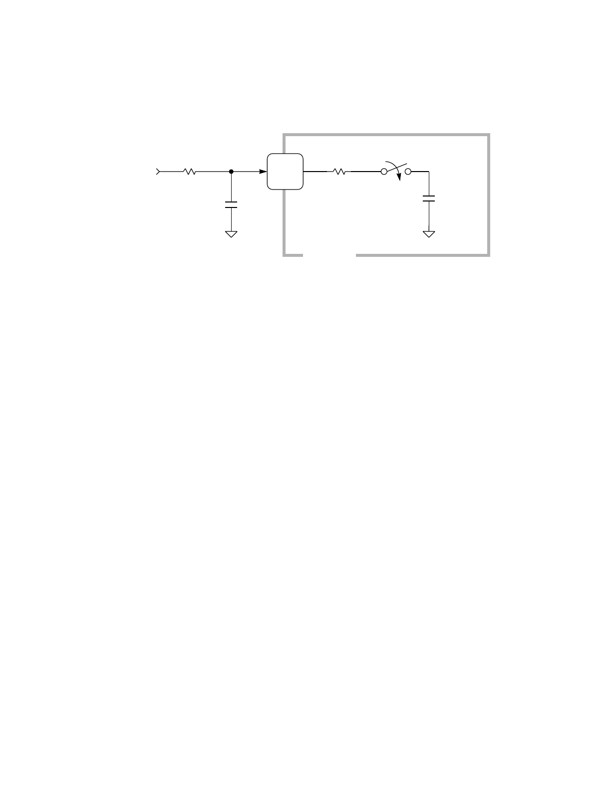
MOTOROLA ANALOG-TO-DIGITAL CONVERTER SYSTEM M68HC11
12-22 REFERENCE MANUAL
analog level. The external series resistance is 10 kΩ, and the external capacitance is
0.01 µF. The value $30 is written to the ADCTL register to initiate continuous round-
robin conversion of channels 0, 1, 2, and 3. The following circuit is a model of the cir-
cuitry under investigation:
RXand CXare the external components, Ciis the internal DAC capacitance, and Riis
the internal series resistance (includes N-channel couplers and polysilicon intercon-
nections). From Figure 12-5,C
iis 20 pF and Riis 4 kΩ. The switch represents an
analog switch closed only during the sample time. For the chosen E-clock rate, the
sample time is 6 µs, and the period from one sample to the next sample of the same
channel is 64 µs.
The voltage change due to redistribution of the residual charge on the DAC capaci-
tance, which is left from conversion of the previous channel, is written as
∆VSAMP = (V1 – V2) [Ci÷ (CX + Ci)]
where V1 = 5.12 V and V2 = 0.0 V
∆VSAMP ≈5.12 (20 pF ÷ 0.01 µF) V
∆VSAMP ≈ 10 mV
Not all of this voltage decays before the second sample; thus, there is an accumulation
of error until an equilibrium is reached. Since this equilibrium voltage is very small rel-
ative to the (V1–V
2) term of this equation, the ∆VSAMP value does not change signif-
icantly between the first sample and a sample time when equilibrium is reached. Since
CX is so large relative to Ci, Ci is ignored in the (CX + Ci) term.
The voltage change between samples of channel 2 is a simple exponential decay
through the external RC, which is written as
∆VHOLD = (VEQ – V2)(1 – e – t/RxCx)
where VEQ is the equilibrium voltage
∆VHOLD = VEQ(1 – e – 64 µs/10K 0.01 µF)
DAC
CAPACITANCE
VRL
ANALOG
INPUT
(PE2 PIN)
~ 20 pF
0.01 µF
DIFFUSION AND
POLY COUPLER
10 kΩ ≤ 4 kΩ
VRL
RX
CX
Ri
Ci
ANALOG
LEVEL
(0.0 V)
COMPONENTS
WITHIN MCU

M68HC11 ANALOG-TO-DIGITAL CONVERTER SYSTEM MOTOROLA
REFERENCE MANUAL 12-23
∆VHOLD = VEQ(1 – e – 0.64)
∆VHOLD = 0.473 VEQ
When equilibrium is reached, the voltage gained during a sample is equal to the volt-
age lost between samples. Therefore, set ∆VHOLD equals ∆VSAMP and solve for VEQ:
0.473 VEQ = 10 mV
VEQ = 10 mV/0.473 ≈21 mV
This value amounts to almost one LSB of error. If the external capacitance is changed
to 0.1 µF, the error attributable to this effect becomes approximately 1 mV. As the ex-
ternal capacitance is changed, two changes occur: first, the time constant of the exter-
nal RC changes; second, the ratio of the external capacitance to the DAC capacitance
changes. Because these two changes influence the result at different rates, it is not
practical to make a general statement about the amount of influence versus the
change in the external capacitance.
For external series resistances not exceeding the recommended limit of 10 kΩ, the er-
rors attributable to this effect are very small. However, if the external series resistance
is increased to 100 kΩand small capacitance values are used, the errors can become
serious. For example, an external RC of 100 kΩand 0.001 µF would cause errors of
about 200 mV in the previous example (about 10 LSBs). The extra leakage effects are
also as much as 40 mV.

MOTOROLA ANALOG-TO-DIGITAL CONVERTER SYSTEM M68HC11
12-24 REFERENCE MANUAL

M68HC11 INSTRUCTION SET DETAILS MOTOROLA
REFERENCE MANUAL A-1
APPENDIX A
INSTRUCTION SET DETAILS
A.1 Introduction
This appendix contains complete detailed information for all M68HC11 instructions.
The instructions are arranged in alphabetical order with the instruction mnemonic set
in larger type for easy reference.
A.2 Nomenclature
The following nomenclature is used in the subsequent definitions.
A. Operators:
( ) = Contents of register shown inside parentheses
⇐= Is transferred to
⇑= Is pulled from stack
⇓= Is pushed onto stack
• = Boolean AND
+ = Arithmetic addition symbol except where used as inclusive-
OR symbol in boolean formula
⊕= Exclusive OR
×= Multiply
: = Concatenation
−= Arithmetic subtraction symbol or negation symbol (two’s
complement)
B. Registers in the MPU
ACCA = Accumulator A
ACCB = Accumulator B
ACCX = Accumulator ACCA or ACCB
ACCD = Double accumulator — Accumulator A concatenated with
accumulator B where A is the most significant byte
CCR = Condition code register
IX = Index register X, 16 bits
IXH = Index register X, high order 8 bits
IXL = Index register X, low order 8 bits
PC = Program counter, 16 bits
PCH = Program counter, high order (most significant) 8 bits
PC = Program counter, low order (least significant) 8 bits
SP = Stack pointer, 16 bits
SPH = Stack pointer, high order 8 bits
SPL = Stack pointer, low order 8 bits

MOTOROLA INSTRUCTION SET DETAILS M68HC11
A-2 REFERENCE MANUAL
C. Memory and Addressing
M = A memory location (one byte)
M+1 = The byte of memory at $0001 plus the address of the mem-
ory location indicated by “M”
Rel = Relative offset (i.e., the two’s complement number stored in
the last byte of machine code corresponding to a branch in-
struction)
(opr) = Operand
(msk) = Mask used in bit manipulation instructions
(rel) = Relative offset used in branch instructions
D. Bits [7:0] of the Condition Code Register
S =Stop disable, bit 7
X = X interrupt mask, bit 6
H = Half carry, bit 5
I = I interrupt mask, bit 4
N = Negative indicator, bit 3
Z = Zero indicator, bit 2
V = Two’s complement overflow indicator, bit 1
C = Carry/borrow, bit 0
E. Status of individual bit before execution of an instruction
An = Bit n of ACCA (n = 7, 6, 5... 0)
Bn = Bit n of ACCB (n = 7, 6, 5... 0)
Dn = Bit n of ACCD (n = 15, 14, 13... 0) where bits [15:8] refer to
ACCA and bits [7:0] refer to ACCB
IXn = Bit n of IX (n = 15, 14, 13... 0)
IXHn = Bit n of IXH (n = 7, 6, 5... 0)
IXLn = Bit n of IXL (n = 7, 6, 5... 0)
IYn = Bit n of IY (n = 15, 14, 13... 0)
IYHn = Bit n of IYH (n = 7, 6, 5... 0)
IYLn = Bit n of IYL (n = 7, 6, 5... 0)
Mn = Bit n of M (n = 7, 6, 5... 0)
SPHn = Bit n of SPH (n = 7, 6, 5... 0)
SPLn = Bit n of SPL (n = 7, 6, 5... 0)
Xn = Bit n of X (n = 7, 6, 5... 0)
F. Status of individual bit of result of execution of an instruction
(i) For 8-bit results:
Rn = Bit n of the result (n = 7, 6, 5... 0). This applies to instructions
which provide a result contained in a single byte of memory or
in an 8-bit register.
(ii) For 16-bit results:
RHn = Bit n of the most significant byte of the result (n = 7, 6, 5... 0)
RLn = Bit n of the least significant byte of the result (n = 7, 6, 5...
0). This applies to instructions which provide a result con-
tained in two consecutive bytes of memory or in a 16-bit reg-
ister.

M68HC11 INSTRUCTION SET DETAILS MOTOROLA
REFERENCE MANUAL A-3
Rn = Bit n of the result (n = 15, 14, 13... 0)
G. Notation used in CCR activity summary figures
— = Bit not affected
0 = Bit forced to zero
1 = Bit forced to one
∆= Bit set or cleared according to results of operation
⇓= Bit may change from one to zero, remain zero, or remain
one as a result of this operation, but cannot change from zero
to one.
H. Notation used in cycle-by-cycle execution tables
— = Irrelevant data
ii = One byte of immediate data
jj = High-order byte of 16-bit immediate data
kk = Low-order byte of 16-bit immediate data
hh = High-order byte of 16-bit extended address
ll = Low-order byte of 16-bit extended address
dd = Low-order eight bits of direct address $0000–$00FF (high
byte assumed to be $00)
mm = 8-bit mask (set bits correspond to operand bits which will be
affected)
ff = 8-bit forward offset $00 (0) to $FF (255) (is added to index)
rr = Signed relative offset $80 (–128) to $7F (+127) (offset rela-
tive to address following machine code offset byte)
OP = Address of opcode byte
OP+n = Address of nth location after opcode byte
SP = Address pointed to by stack pointer value (at the start of an
instruction)
SP+n = Address of nth higher address past that pointed to by stack
pointer
SP–n = Address of nth lower address before that pointed to by stack
pointer
Sub =Address of called subroutine
Nxt op = Opcode of next instruction
Rtn hi = High-order byte of return address
Rtn lo = Low-order byte of return address
Svc hi = High-order byte of address for service routine
Svc lo = Low-order byte of address for service routine
Vec hi = High-order byte of interrupt vector
Vec lo = Low-order byte of interrupt vector
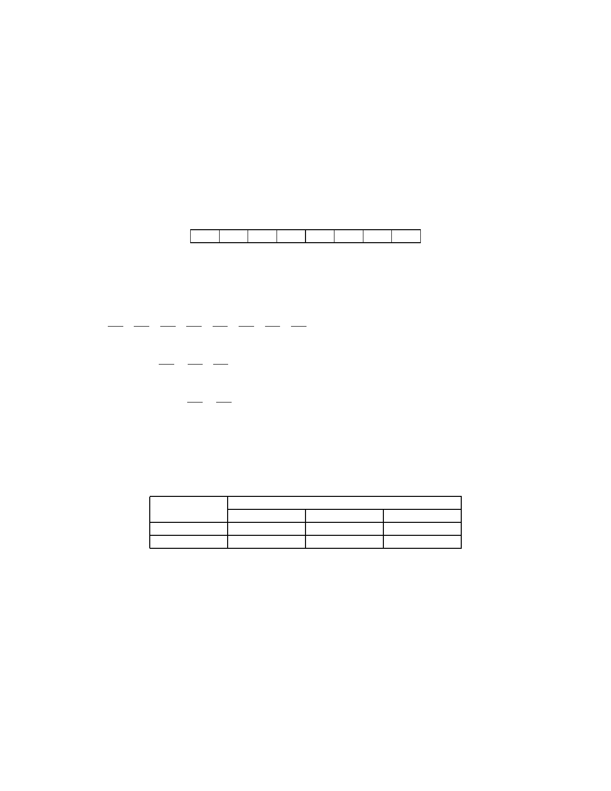
MOTOROLA INSTRUCTION SET DETAILS M68HC11
A-4 REFERENCE MANUAL
ABA Add Accumulator B to Accumulator A ABA
Operation: ACCA ⇐(ACCA) + (ACCB)
Description: Adds the contents of accumulator B to the contents of accumulator A and
places the result in accumulator A. Accumulator B is not changed. This instruction
affects the H condition code bit so it is suitable for use in BCD arithmetic operations
(see DAA instruction for additional information).
Condition Codes and Boolean Formulae:
H A3 • B3 + B3 • R3 + R3 • A3
Set if there was a carry from bit 3; cleared otherwise.
NR7
Set if MSB of result is set; cleared otherwise.
ZR7 • R6 • R5 • R4 • R3 • R2 • R1 • R0
Set if result is $00; cleared otherwise.
V A7 • B7 • R7 + A7 • B7 • R7
Set if a two’s complement overflow resulted from the operation; cleared otherwise.
C A7 • B7 + B7 • R7 + R7 • A7
Set if there was a carry from the MSB of the result; cleared otherwise.
Source Forms: ABA
Addressing Modes, Machine Code, and Cycle-by-Cycle Execution:
SXHINZVC
—— ∆—∆∆∆∆
Cycle ABA (INH)
Addr Data R/W
1OP1B1
2 OP+1 — 1
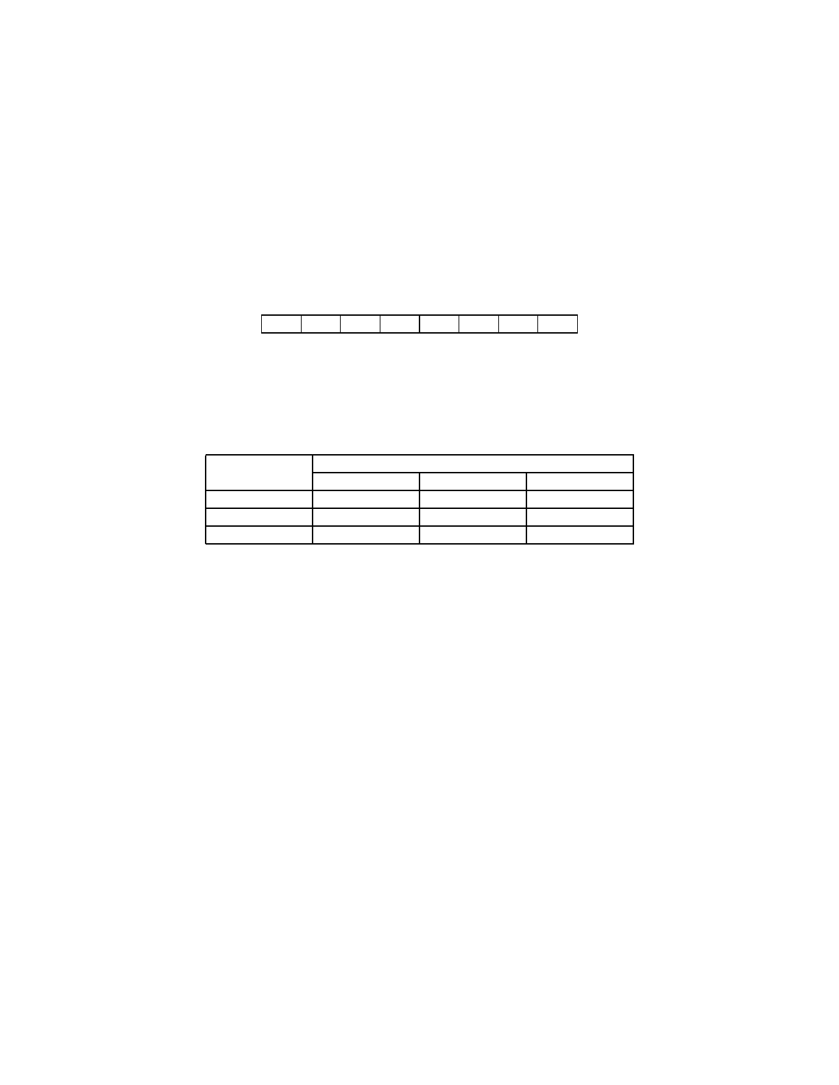
M68HC11 INSTRUCTION SET DETAILS MOTOROLA
REFERENCE MANUAL A-5
ABX Add Accumulator B to Index Register X ABX
Operation: IX ⇐(IX) + (ACCB)
Description: Adds the 8-bit unsigned contents of accumulator B to the contents of index
register X (IX) considering the possible carry out of the low-order byte of the index
register X; places the result in index register X (IX). Accumulator B is not changed.
There is no equivalent instruction to add accumulator A to an index register.
Condition Codes and Boolean Formulae:
None affected
Source Forms: ABX
Addressing Modes, Machine Code, and Cycle-by-Cycle Execution:
SXHINZVC
————————
Cycle ABX (INH)
Addr Data R/W
1OP3A1
2 OP+1 — 1
3 FFFF — 1

MOTOROLA INSTRUCTION SET DETAILS M68HC11
A-6 REFERENCE MANUAL
ABY Add Accumulator B to Index Register Y ABY
Operation: IY ⇐(IY) + (ACCB)
Description: Adds the 8-bit unsigned contents of accumulator B to the contents of index
register Y (IY) considering the possible carry out of the low-order byte of the index
register Y; places the result in index register Y (IY). Accumulator B is not changed.
There is no equivalent instruction to add accumulator A to an index register.
Condition Codes and Boolean Formulae:
None affected
Source Forms: ABY
Addressing Modes, Machine Code, and Cycle-by-Cycle Execution:
SXHINZVC
————————
Cycle ABY (INH)
Addr Data R/W
1OP1B1
2 OP+1 3A 1
3 OP+2 — 1
4 FFFF — 1
M68HC11 INSTRUCTION SET DETAILS MOTOROLA
REFERENCE MANUAL A-7
ADC Add with Carry ADC
Operation: ACCX ⇐(ACCX) + (M) + (C)
Description: Adds the contents of the C bit to the sum of the contents of ACCX and M
and places the result in ACCX. This instruction affects the H condition code bit so
it is suitable for use in BCD arithmetic operations (see DAA instruction for addition-
al information).
Condition Codes and Boolean Formulae:
H X3 • M3 + M3 • R3 + R3 • X3
Set if there was a carry from bit 3; cleared otherwise.
NR7
Set if MSB of result is set; cleared otherwise.
ZR7 • R6 • R5 • R4 • R3 • R2 • R1 • R0
Set if result is $00; cleared otherwise.
V X7 • M7 • R7 + X7 • M7 • R7
Set if a two’s complement overflow resulted from the operation; cleared otherwise.
C X7 • M7 + M7 • R7 + R7 • X7
Set if there was a carry from the MSB of the result; cleared otherwise.
Source Forms: ADCA (opr); ADCB (opr)
Addressing Modes, Machine Code, and Cycle-by-Cycle Execution:
SXHINZVC
—— ∆—∆∆∆∆
Cycle ADCA(IMM) ADCA (DIR) ADCA (EXT) ADCA (IND,X) ADCA (IND,Y)
Addr Data R/W Addr Data R/W Addr Data R/W Addr Data R/W Addr Data R/W
1 OP 89 1 OP 99 1 OP B9 1 OP A9 1 OP 18 1
2 OP+1 ii 1 OP+1 dd 1 OP+1 hh 1 OP+1 ff 1 OP+1 A9 1
3 00dd (00dd
)1 OP+2 ll 1 FFFF — 1 OP+2 ff 1
4 hhll (hhll) 1 X+ff (X+ff) 1 FFFF — 1
5 Y+ff (Y+ff) 1
Cycle ADCB (IMM) ADCB (DIR) ADCB (EXT) ADCB (IND,X) ADCB (IND,Y)
Addr Data R/W Addr Data R/W Addr Data R/W Addr Data R/W Addr Data R/W
1 OP C9 1 OP D9 1 OP F9 1 OP E9 1 OP 18 1
2 OP+1 ii 1 OP+1 dd 1 OP+1 hh 1 OP+1 ff 1 OP+1 E9 1
3 00dd (00dd
)1 OP+2 ll 1 FFFF — 1 OP+2 ff 1
4 hhll (hhll) 1 X+ff (X+ff) 1 FFFF — 1
5 Y+ff (Y+ff) 1
MOTOROLA INSTRUCTION SET DETAILS M68HC11
A-8 REFERENCE MANUAL
ADD Add without Carry ADD
Operation: ACCX ⇐(ACCX) + (M)
Description: Adds the contents of M to the contents of ACCX and places the result in AC-
CX. This instruction affects the H condition code bit so it is suitable for use in BCD
arithmetic operations (see DAA instruction for additional information).
Condition Codes and Boolean Formulae:
H X3 • M3 + M3 • R3 + R3 • X3
Set if there was a carry from bit 3; cleared otherwise.
NR7
Set if MSB of result is set; cleared otherwise.
ZR7 • R6 • R5 • R4 • R3 • R2 • R1 • R0
Set if result is $00; cleared otherwise.
V X7 • M7 • R7 + X7 • M7 • R7
Set if a two’s complement overflow resulted from the operation; cleared otherwise.
C X7 • M7 + M7 • R7 + R7 • X7
Set if there was a carry from the MSB of the result; cleared otherwise.
Source Forms: ADDA (opr); ADDB (opr)
Addressing Modes, Machine Code, and Cycle-by-Cycle Execution:
SXHINZVC
—— ∆—∆∆∆∆
Cycle ADDA(IMM) ADDA (DIR) ADDA (EXT) ADDA (IND,X) ADDA (IND,Y)
Addr Data R/W Addr Data R/W Addr Data R/W Addr Data R/W Addr Data R/W
1 OP BB 1 OP 9B 1 OP BB 1 OP AB 1 OP 18 1
2 OP+1 ii 1 OP+1 dd 1 OP+1 hh 1 OP+1 ff 1 OP+1 AB 1
3 00dd (00dd
)1 OP+2 ll 1 FFFF — 1 OP+2 ff 1
4 hhll (hhll) 1 X+ff (X+ff) 1 FFFF — 1
5 Y+ff (Y+ff) 1
Cycle ADDB (IMM) ADDB (DIR) ADDB (EXT) ADDB (IND,X) ADDB (IND,Y)
Addr Data R/W Addr Data R/W Addr Data R/W Addr Data R/W Addr Data R/W
1 OP CB 1 OP DB 1 OP FB 1 OP EB 1 OP 18 1
2 OP+1 ii 1 OP+1 dd 1 OP+1 hh 1 OP+1 ff 1 OP+1 EB 1
3 00dd (00dd
)1 OP+2 ll 1 FFFF — 1 OP+2 ff 1
4 hhll (hhll) 1 X+ff (X+ff) 1 FFFF — 1
5 Y+ff (Y+ff) 1
M68HC11 INSTRUCTION SET DETAILS MOTOROLA
REFERENCE MANUAL A-9
ADDD Add Double Accumulator ADDD
Operation: ACCD ⇐(ACCD) + (M : M + 1)
Description: Adds the contents of M concatenated with M + 1 to the contents of ACCD
and places the result in ACCD. Accumulator A corresponds to the high-order half
of the 16-bit double accumulator D.
Condition Codes and Boolean Formulae:
N R15
Set if MSB of result is set; cleared otherwise.
ZR15 • R14 • R13 • R12 • R11 • R10 • R9 • R8 • R7 • R6 • R5 • R4 • R3 • R2 • R1 • R0
Set if result is $0000; cleared otherwise.
V D15 • M15 • R15 + D15 • M15 • R15
Set if a two’s complement overflow resulted from the operation; cleared otherwise.
C D15 • M15 + M15 • R15 + R15 • D15
Set if there was a carry from the MSB of the result; cleared otherwise.
Source Forms: ADDD (opr)
Addressing Modes, Machine Code, and Cycle-by-Cycle Execution:
SXHINZVC
———— ∆∆∆∆
Cycle ADDD (IMM) ADDD (DIR) ADDD (EXT) ADDD (IND,X) ADDD (IND,Y)
Addr Data R/W Addr Data R/W Addr Data R/W Addr Data R/W Addr Data R/W
1 OP C3 1 OP D3 1 OP F3 1 OP E3 1 OP 18 1
2 OP+1 jj 1 OP+1 dd 1 OP+1 hh 1 OP+1 ff 1 OP+1 E3 1
3 OP+2 kk 1 00dd (00dd) 1 OP+2 ll 1 FFFF — 1 OP+2 ff 1
4 FFFF — 1 00dd+1 (00dd+1
)1 hhll (hhll) 1 X+ff (X+ff) 1 FFFF — 1
5 FFFF — 1 hhll+1 (hhll+1) 1 X+ff+
1(X+ff+1
)1 Y+ff (Y+ff) 1
6 FFFF — 1 FFFF — 1 Y+ff+
1(Y+ff+1
)1
7 FFFF — 1
MOTOROLA INSTRUCTION SET DETAILS M68HC11
A-10 REFERENCE MANUAL
AND Logical AND AND
Operation: ACCX ⇐(ACCX) + (M)
Description: Performs the logical AND between the contents of ACCX and the contents
of M and places the result in ACCX. (Each bit of ACCX after the operation will be
the logical AND of the corresponding bits of M and of ACCX before the operation.)
Condition Codes and Boolean Formulae:
NR7
Set if MSB of result is set; cleared otherwise.
ZR7 • R6 • R5 • R4 • R3 • R2 • R1 • R0
Set if result is $00; cleared otherwise.
V0
Cleared
Source Forms: ANDA (opr); ANDB (opr)
Addressing Modes, Machine Code, and Cycle-by-Cycle Execution:
SXHINZVC
———— ∆∆0—
Cycle ANDA(IMM) ANDA (DIR) ANDA (EXT) ANDA (IND,X) ANDA (IND,Y)
Addr Data R/W Addr Data R/W Addr Data R/W Addr Data R/W Addr Data R/W
1 OP 84 1 OP 94 1 OP B4 1 OP A4 1 OP 18 1
2 OP+1 ii 1 OP+1 dd 1 OP+1 hh 1 OP+1 ff 1 OP+1 AB 1
3 00dd (00dd
)1 OP+2 ll 1 FFFF — 1 OP+2 ff 1
4 hhll (hhll) 1 X+ff (X+ff) 1 FFFF — 1
5 Y+ff (Y+ff) 1
Cycle ANDB (IMM) ANDB (DIR) ANDB (EXT) ANDB (IND,X) ANDB (IND,Y)
Addr Data R/W Addr Data R/W Addr Data R/W Addr Data R/W Addr Data R/W
1 OP C4 1 OP D4 1 OP F4 1 OP E4 1 OP 18 1
2 OP+1 ii 1 OP+1 dd 1 OP+1 hh 1 OP+1 ff 1 OP+1 EB 1
3 00dd (00dd
)1 OP+2 ll 1 FFFF — 1 OP+2 ff 1
4 hhll (hhll) 1 X+ff (X+ff) 1 FFFF — 1
5 Y+ff (Y+ff) 1
M68HC11 INSTRUCTION SET DETAILS MOTOROLA
REFERENCE MANUAL A-11
ASL Arithmetic Shift Left ASL
(Same as LSL)
Operation:
Description: Shifts all bits of the ACCX or M one place to the left. Bit 0 is loaded with a
zero. The C bit in the CCR is loaded from the most significant bit of ACCX or M.
Condition Codes and Boolean Formulae:
NR7
Set if MSB of result is set; cleared otherwise.
ZR7 • R6 • R5 • R4 • R3 • R2 • R1 • R0
Set if result is $00; cleared otherwise.
VN⊕C = [N • C] + [N • C] (for N and C after the shift)
Set if (N is set and C is clear) or (N is clear and C is set); cleared otherwise (for
values of N and C after the shift).
CM7
Set if, before the shift, the MSB of ACCX or M was set; cleared otherwise.
Source Forms: ASLA; ASLB; ASL (opr)
Addressing Modes, Machine Code, and Cycle-by-Cycle Execution:
SXHINZVC
———— ∆∆∆∆
Cycle ASLA (IMM) ASLB (DIR) ASL (EXT) ASL (IND,X) ASL (IND,Y)
Addr Data R/W Addr Data R/W Addr Data R/W Addr Data R/W Addr Data R/W
1 OP 48 1 OP 58 1 OP 78 1 OP 68 1 OP 18 1
2 OP+1 — 1 OP+1 — 1 OP+1 hh 1 OP+1 ff 1 OP+1 68 1
3 OP+2 ll 1 FFFF — 1 OP+2 ff 1
4 hhll (hhll) 1 X+ff (X+ff) 1 FFFF — 1
5 FFFF — 1 FFFF — 1 Y+ff (Y+ff) 1
6 hhll result 0 X+ff result 0 FFFF — 1
7 Y+ff result 0
Cb7 – – – – – – b0 0
MOTOROLA INSTRUCTION SET DETAILS M68HC11
A-12 REFERENCE MANUAL
ASLD Arithmetic Shift Left Double Accumulator ASLD
(Same as LSLD)
Operation:
Description: Shifts all bits of ACCD one place to the left. Bit 0 is loaded with a zero. The
C bit in the CCR is loaded from the most significant bit of ACCD.
Condition Codes and Boolean Formulae:
N R15
Set if MSB of result is set; cleared otherwise.
ZR15 • R14 • R13 • R12 • R11 • R10 • R9 • R8 • R7 • R6 • R5 • R4 • R3 • R2 • R1 • R0
Set if result is $0000; cleared otherwise.
VN⊕C = [N • C] + [N • C] (for N and C after the shift)
Set if (N is set and C is clear) or (N is clear and C is set); cleared otherwise (for
values of N and C after the shift).
C D15
Set if, before the shift, the MSB of ACCD was set; cleared otherwise.
Source Forms: ASLD (opr)
Addressing Modes, Machine Code, and Cycle-by-Cycle Execution:
SXHINZVC
———— ∆∆∆∆
Cycle ASLD (INH)
Addr Data R/W
1OP05 1
2 OP+1 — 1
3 FFFF — 1
C b7 – – – – – – b0 b7 – – – – – – b0 0
ACCA ACCB
M68HC11 INSTRUCTION SET DETAILS MOTOROLA
REFERENCE MANUAL A-13
ASR Arithmetic Shift Right ASR
Operation:
Description: Shifts all bits of the ACCX or M one place to the right. Bit 7 is held constant.
Bit 0 is loaded into the C bit of the CCR. This operation effectively divides a two’s
complement value by two without changing its sign. The carry bit can be used to
round the result.
Condition Codes and Boolean Formulae:
NR7
Set if MSB of result is set; cleared otherwise.
ZR7 • R6 • R5 • R4 • R3 • R2 • R1 • R0
Set if result is $00; cleared otherwise.
VN⊕C = [N • C] + [N • C] (for N and C after the shift)
Set if (N is set and C is clear) or (N is clear and C is set); cleared otherwise (for
values of N and C after the shift).
CM0
Set if, before the shift, the LSB of ACCX or M was set; cleared otherwise.
Source Forms: ASRA; ASRB; ASR (opr)
Addressing Modes, Machine Code, and Cycle-by-Cycle Execution:
SXHINZVC
———— ∆∆∆∆
Cycle ASRA (IMM) ASRB (DIR) ASR (EXT) ASR (IND,X) ASR (IND,Y)
Addr Data R/W Addr Data R/W Addr Data R/W Addr Data R/W Addr Data R/W
1 OP 47 1 OP 57 1 OP 77 1 OP 67 1 OP 18 1
2 OP+1 — 1 OP+1 — 1 OP+1 hh 1 OP+1 ff 1 OP+1 68 1
3 OP+2 ll 1 FFFF — 1 OP+2 ff 1
4 hhll (hhll) 1 X+ff (X+ff) 1 FFFF — 1
5 FFFF — 1 FFFF — 1 Y+ff (Y+ff) 1
6 hhll result 0 X+ff result 0 FFFF — 1
7 Y+ff result 0
C
b7 – – – – – – b0

MOTOROLA INSTRUCTION SET DETAILS M68HC11
A-14 REFERENCE MANUAL
BCC Branch if Carry Clear BCC
(Same as BHS)
Operation: PC ⇐ (PC) + $0002 + Rel if (C) = 0
Description: Tests the state of the C bit in the CCR and causes a branch if C is clear.
See BRA instruction for further details of the execution of the branch.
Condition Codes and Boolean Formulae:
None affected
Source Forms: BCC (rel)
Addressing Modes, Machine Code, and Cycle-by-Cycle Execution:
The following table is a summary of all branch instructions.
SXHINZVC
————————
Cycle BCC (INH)
Addr Data R/W
1OP24 1
2 OP+1 rr 1
3 FFFF — 1
Test Boolean Mnemonic Opcode Complementary Branch Comment
r>m Z+(N⊕V)=0 BGT 2E r≤m BLE 2F Signed
r≥mN⊕V=0 BGE 2C r<m BLT 2D Signed
r=m Z=1 BEQ 27 r≠m BNE 26 Signed
r≤m Z+(N⊕V)=1 BLE 2F r>m BGT 2E Signed
r<m N⊕V=1 BLT 2D r≥m BGE 2C Signed
r>m C+Z=0 BHI 22 r≤m BLS 23 Unsigned
r≥m C=0 BHS/BCC 24 r<m BLO/BCS 25 Unsigned
r=m Z=1 BEQ 27 r≠m BNE 26 Unsigned
r≤m C+Z=1 BLS 23 r>m BHI 22 Unsigned
r<m C=1 BLO/BCS 25 r≥m BHS/BCC 24 Unsigned
Carry C=1 BCS 25 No Carry BCC 24 Simple
Negative N=1 BMI 2B Plus BPL 2A Simple
Overflow V=1 BVS 29 No Overflow BVC 28 Simple
r=0 Z=1 BEQ 27 r≠0 BNE 26 Simple
Always — BRA 20 Never BRN 21 Unconditional
M68HC11 INSTRUCTION SET DETAILS MOTOROLA
REFERENCE MANUAL A-15
BCLR Clear Bit(s) in Memory BCLR
Operation: M⇐(M) • (PC + 2)
M⇐(M) • (PC + 3) (for IND,Y address mode only)
Description: Clear multiple bits in location M. The bit(s) to be cleared are specified by
ones in the mask byte. All other bits in M are rewritten to their current state.
Condition Codes and Boolean Formulae:
NR7
Set if MSB of result is set; cleared otherwise.
ZR7 • R6 • R5 • R4 • R3 • R2 • R1 • R0
Set if result is $00; cleared otherwise.
V0
Cleared
Source Forms: BCLR (opr) (msk)
Addressing Modes, Machine Code, and Cycle-by-Cycle Execution:
SXHINZVC
———— ∆∆0—
Cycle BCLR (DIR) BCLR (IND,X) BCLR (IND,Y)
Addr Data R/W Addr Data R/W Addr Data R/W
1 OP 15 1 OP 1D 1 OP 18 1
2 OP+1 dd 1 OP+1 ff 1 OP+1 1D 1
3 00dd (00dd) 1 FFFF — 1 OP+2 ff 1
4 OP+2 MM 1 X+ff (X+ff) 1 FFFF — 1
5 FFFF — 1 OP+2 MM 1 (IY)+ff (Y+ff) 1
6 00dd result 0 FFFF — 1 OP+3 mm 1
7 X+ff result 0 FFFF — 1
8 Y+ff result 0
MOTOROLA INSTRUCTION SET DETAILS M68HC11
A-16 REFERENCE MANUAL
BCS Branch if Carry Set BCS
(Same as BLO)
Operation: PC⇐(PC)+ $0002 + Rel if (C) = 1
Description: Tests the state of the C bit in the CCR and causes a branch if C is set. See
BRA instruction for further details of the execution of the branch.
Condition Codes and Boolean Formulae:
None affected
Source Forms: BCS (rel)
Addressing Modes, Machine Code, and Cycle-by-Cycle Execution:
The following table is a summary of all branch instructions.
SXHINZVC
————————
Cycle BCS (REL)
Addr Data R/W
1OP25 1
2 OP+1 rr 1
3 FFFF — 1
Test Boolean Mnemonic Opcode Complementary Branch Comment
r>m Z+(N⊕V)=0 BGT 2E r≤m BLE 2F Signed
r≥mN⊕V=0 BGE 2C r<m BLT 2D Signed
r=m Z=1 BEQ 27 r≠m BNE 26 Signed
r≤m Z+(N⊕V)=1 BLE 2F r>m BGT 2E Signed
r<m N⊕V=1 BLT 2D r≥m BGE 2C Signed
r>m C+Z=0 BHI 22 r≤m BLS 23 Unsigned
r≥m C=0 BHS/BCC 24 r<m BLO/BCS 25 Unsigned
r=m Z=1 BEQ 27 r≠m BNE 26 Unsigned
r≤m C+Z=1 BLS 23 r>m BHI 22 Unsigned
r<m C=1 BLO/BCS 25 r≥m BHS/BCC 24 Unsigned
Carry C=1 BCS 25 No Carry BCC 24 Simple
Negative N=1 BMI 2B Plus BPL 2A Simple
Overflow V=1 BVS 29 No Overflow BVC 28 Simple
r=0 Z=1 BEQ 27 r≠0 BNE 26 Simple
Always — BRA 20 Never BRN 21 Unconditional
M68HC11 INSTRUCTION SET DETAILS MOTOROLA
REFERENCE MANUAL A-17
BEQ Branch if Equal BEQ
Operation: PC⇐(PC)+ $0002 + Rel if (Z) = 1
Description: Tests the state of the Z bit in the CCR and causes a branch if Z is set. See
BRA instruction for further details of the execution of the branch.
Condition Codes and Boolean Formulae:
None affected
Source Forms: BEQ (rel)
Addressing Modes, Machine Code, and Cycle-by-Cycle Execution:
The following table is a summary of all branch instructions.
SXHINZVC
————————
Cycle BEQ (REL)
Addr Data R/W
1OP27 1
2 OP+1 rr 1
3 FFFF — 1
Test Boolean Mnemonic Opcode Complementary Branch Comment
r>m Z+(N⊕V)=0 BGT 2E r≤m BLE 2F Signed
r≥mN⊕V=0 BGE 2C r<m BLT 2D Signed
r=m Z=1 BEQ 27 r≠m BNE 26 Signed
r≤m Z+(N⊕V)=1 BLE 2F r>m BGT 2E Signed
r<m N⊕V=1 BLT 2D r≥m BGE 2C Signed
r>m C+Z=0 BHI 22 r≤m BLS 23 Unsigned
r≥m C=0 BHS/BCC 24 r<m BLO/BCS 25 Unsigned
r=m Z=1 BEQ 27 r≠m BNE 26 Unsigned
r≤m C+Z=1 BLS 23 r>m BHI 22 Unsigned
r<m C=1 BLO/BCS 25 r≥m BHS/BCC 24 Unsigned
Carry C=1 BCS 25 No Carry BCC 24 Simple
Negative N=1 BMI 2B Plus BPL 2A Simple
Overflow V=1 BVS 29 No Overflow BVC 28 Simple
r=0 Z=1 BEQ 27 r≠0 BNE 26 Simple
Always — BRA 20 Never BRN 21 Unconditional
MOTOROLA INSTRUCTION SET DETAILS M68HC11
A-18 REFERENCE MANUAL
BGE Branch if Greater than or Equal to Zero BGE
Operation: PC⇐(PC)+ $0002 + Rel if (N) ⊕(V) = 0
i.e., if (ACCX)≤(M) (two’s-complement signed numbers)
Description: If the BGE instruction is executed immediately after execution of any of the
instructions, CBA, CMP(A, B, or D), CP(X or Y), SBA, SUB(A, B, or D), the branch
will occur if and only if the two’s complement number represented by ACCX was
greater than or equal to the two’s complement number represented by M.
See BRA instruction for further details of the execution of the branch.
Condition Codes and Boolean Formulae:
None affected
Source Forms: BGE (rel)
Addressing Modes, Machine Code, and Cycle-by-Cycle Execution:
The following table is a summary of all branch instructions.
SXHINZVC
————————
Cycle BGE (REL)
Addr Data R/W
1OP2C1
2 OP+1 rr 1
3 FFFF — 1
Test Boolean Mnemonic Opcode Complementary Branch Comment
r>m Z+(N⊕V)=0 BGT 2E r≤m BLE 2F Signed
r≥mN⊕V=0 BGE 2C r<m BLT 2D Signed
r=m Z=1 BEQ 27 r≠m BNE 26 Signed
r≤m Z+(N⊕V)=1 BLE 2F r>m BGT 2E Signed
r<m N⊕V=1 BLT 2D r≥m BGE 2C Signed
r>m C+Z=0 BHI 22 r≤m BLS 23 Unsigned
r≥m C=0 BHS/BCC 24 r<m BLO/BCS 25 Unsigned
r=m Z=1 BEQ 27 r≠m BNE 26 Unsigned
r≤m C+Z=1 BLS 23 r>m BHI 22 Unsigned
r<m C=1 BLO/BCS 25 r≥m BHS/BCC 24 Unsigned
Carry C=1 BCS 25 No Carry BCC 24 Simple
Negative N=1 BMI 2B Plus BPL 2A Simple
Overflow V=1 BVS 29 No Overflow BVC 28 Simple
r=0 Z=1 BEQ 27 r≠0 BNE 26 Simple
Always — BRA 20 Never BRN 21 Unconditional

M68HC11 INSTRUCTION SET DETAILS MOTOROLA
REFERENCE MANUAL A-19
BGT Branch if Greater than Zero BGT
Operation: PC⇐(PC)+ $0002 + Rel if (Z) + [(N) ⊕(V)] = 0
i.e., if (ACCX)>(M) (two’s-complement signed numbers)
Description: If the BGT instruction is executed immediately after execution of any of the
instructions, CBA, CMP(A, B, or D), CP(X or Y), SBA, SUB(A, B, or D), the branch
will occur if and only if the two’s complement number represented by ACCX was
greater than the two’s complement number represented by M.
See BRA instruction for further details of the execution of the branch.
Condition Codes and Boolean Formulae:
None affected
Source Forms: BGT (rel)
Addressing Modes, Machine Code, and Cycle-by-Cycle Execution:
The following table is a summary of all branch instructions.
SXHINZVC
————————
Cycle BGT (REL)
Addr Data R/W
1OP2E1
2 OP+1 rr 1
3 FFFF — 1
Test Boolean Mnemonic Opcode Complementary Branch Comment
r>m Z+(N⊕V)=0 BGT 2E r≤m BLE 2F Signed
r≥mN⊕V=0 BGE 2C r<m BLT 2D Signed
r=m Z=1 BEQ 27 r≠m BNE 26 Signed
r≤m Z+(N⊕V)=1 BLE 2F r>m BGT 2E Signed
r<m N⊕V=1 BLT 2D r≥m BGE 2C Signed
r>m C+Z=0 BHI 22 r≤m BLS 23 Unsigned
r≥m C=0 BHS/BCC 24 r<m BLO/BCS 25 Unsigned
r=m Z=1 BEQ 27 r≠m BNE 26 Unsigned
r≤m C+Z=1 BLS 23 r>m BHI 22 Unsigned
r<m C=1 BLO/BCS 25 r≥m BHS/BCC 24 Unsigned
Carry C=1 BCS 25 No Carry BCC 24 Simple
Negative N=1 BMI 2B Plus BPL 2A Simple
Overflow V=1 BVS 29 No Overflow BVC 28 Simple
r=0 Z=1 BEQ 27 r≠0 BNE 26 Simple
Always — BRA 20 Never BRN 21 Unconditional
MOTOROLA INSTRUCTION SET DETAILS M68HC11
A-20 REFERENCE MANUAL
BHI Branch if Higher BHI
Operation: PC⇐(PC)+ $0002 + Rel if (C) + (Z) = 0
i.e., if (ACCX)>(M) (unsigned binary numbers)
Description: If the BHI instruction is executed immediately after execution of any of the
instructions, CBA, CMP(A, B, or D), CP(X or Y), SBA, SUB(A, B, or D), the branch
will occur if and only if the unsigned binary number represented by ACCX was
greater than unsigned binary number represented by M. Generally not useful after
INC/DEC, LD/ST, TST/CLR/COM because these instructions do not affect the C
bit in the CCR.
See BRA instruction for further details of the execution of the branch.
Condition Codes and Boolean Formulae:
None affected
Source Forms: BHI (rel)
Addressing Modes, Machine Code, and Cycle-by-Cycle Execution:
The following table is a summary of all branch instructions.
SXHINZVC
————————
Cycle BHI (REL)
Addr Data R/W
1OP22 1
2 OP+1 rr 1
3 FFFF — 1
Test Boolean Mnemonic Opcode Complementary Branch Comment
r>m Z+(N⊕V)=0 BGT 2E r≤m BLE 2F Signed
r≥mN⊕V=0 BGE 2C r<m BLT 2D Signed
r=m Z=1 BEQ 27 r≠m BNE 26 Signed
r≤m Z+(N⊕V)=1 BLE 2F r>m BGT 2E Signed
r<m N⊕V=1 BLT 2D r≥m BGE 2C Signed
r>m C+Z=0 BHI 22 r≤m BLS 23 Unsigned
r≥m C=0 BHS/BCC 24 r<m BLO/BCS 25 Unsigned
r=m Z=1 BEQ 27 r≠m BNE 26 Unsigned
r≤m C+Z=1 BLS 23 r>m BHI 22 Unsigned
r<m C=1 BLO/BCS 25 r≥m BHS/BCC 24 Unsigned
Carry C=1 BCS 25 No Carry BCC 24 Simple
Negative N=1 BMI 2B Plus BPL 2A Simple
Overflow V=1 BVS 29 No Overflow BVC 28 Simple
r=0 Z=1 BEQ 27 r≠0 BNE 26 Simple
Always — BRA 20 Never BRN 21 Unconditional
M68HC11 INSTRUCTION SET DETAILS MOTOROLA
REFERENCE MANUAL A-21
BHS Branch if Higher or Same BHS
(Same as BCC)
Operation: PC⇐(PC)+ $0002 + Rel if (C) = 0
i.e., if (ACCX)≥(M) (unsigned binary numbers)
Description: If the BHS instruction is executed immediately after execution of any of the
instructions, CBA, CMP(A, B, or D), CP(X or Y), SBA, SUB(A, B, or D), the branch
will occur if and only if the unsigned binary number represented by ACCX was
greater than or equal to the unsigned binary number represented by M. Generally
not useful after INC/DEC, LD/ST, TST/CLR/COM because these instructions do
not affect the C bit in the CCR.
See BRA instruction for further details of the execution of the branch.
Condition Codes and Boolean Formulae:
None affected
Source Forms: BHS (rel)
Addressing Modes, Machine Code, and Cycle-by-Cycle Execution:
The following table is a summary of all branch instructions.
SXHINZVC
————————
Cycle BHS (REL)
Addr Data R/W
1OP24 1
2 OP+1 rr 1
3 FFFF — 1
Test Boolean Mnemonic Opcode Complementary Branch Comment
r>m Z+(N⊕V)=0 BGT 2E r≤m BLE 2F Signed
r≥mN⊕V=0 BGE 2C r<m BLT 2D Signed
r=m Z=1 BEQ 27 r≠m BNE 26 Signed
r≤m Z+(N⊕V)=1 BLE 2F r>m BGT 2E Signed
r<m N⊕V=1 BLT 2D r≥m BGE 2C Signed
r>m C+Z=0 BHI 22 r≤m BLS 23 Unsigned
r≥m C=0 BHS/BCC 24 r<m BLO/BCS 25 Unsigned
r=m Z=1 BEQ 27 r≠m BNE 26 Unsigned
r≤m C+Z=1 BLS 23 r>m BHI 22 Unsigned
r<m C=1 BLO/BCS 25 r≥m BHS/BCC 24 Unsigned
Carry C=1 BCS 25 No Carry BCC 24 Simple
Negative N=1 BMI 2B Plus BPL 2A Simple
Overflow V=1 BVS 29 No Overflow BVC 28 Simple
r=0 Z=1 BEQ 27 r≠0 BNE 26 Simple
Always — BRA 20 Never BRN 21 Unconditional

MOTOROLA INSTRUCTION SET DETAILS M68HC11
A-22 REFERENCE MANUAL
BIT Bit Test BIT
Operation: (ACCX)•(M)
Description: Performs the logical AND between the contents of ACCX and the contents
of M and modifies the condition codes accordingly. Neither the contents of ACCX
or M operands are affected. (Each bit of the result of the AND would be the logical
AND of the corresponding bits of ACCX and M.)
Condition Codes and Boolean Formulae:
NR7
Set if MSB of result is set; cleared otherwise.
ZR7 • R6 • R5 • R4 • R3 • R2 • R1 • R0
Set if result is $00; cleared otherwise.
V0
Cleared
Source Forms: BITA (opr); BITB (opr)
Addressing Modes, Machine Code, and Cycle-by-Cycle Execution:
SXHINZVC
———— ∆∆0—
Cycle BITA(IMM) BITA (DIR) BITA (EXT) BITA (IND,X) BITA (IND,Y)
Addr Data R/W Addr Data R/W Addr Data R/W Addr Data R/W Addr Data R/W
1 OP 85 1 OP 95 1 OP B5 1 OP A5 1 OP 18 1
2 OP+1 ii 1 OP+1 dd 1 OP+1 hh 1 OP+1 ff 1 OP+1 AB 1
3 00dd (00dd
)1 OP+2 ll 1 FFFF — 1 OP+2 ff 1
4 hhll (hhll) 1 X+ff (X+ff) 1 FFFF — 1
5 Y+ff (Y+ff) 1
Cycle BITB (IMM) BITB (DIR) BITB (EXT) BITB (IND,X) BITB (IND,Y)
Addr Data R/W Addr Data R/W Addr Data R/W Addr Data R/W Addr Data R/W
1 OP C5 1 OP D5 1 OP F5 1 OP E5 1 OP 18 1
2 OP+1 ii 1 OP+1 dd 1 OP+1 hh 1 OP+1 ff 1 OP+1 EB 1
3 00dd (00dd
)1 OP+2 ll 1 FFFF — 1 OP+2 ff 1
4 hhll (hhll) 1 X+ff (X+ff) 1 FFFF — 1
5 Y+ff (Y+ff) 1

M68HC11 INSTRUCTION SET DETAILS MOTOROLA
REFERENCE MANUAL A-23
BLE Branch if Less than or Equal to Zero BLE
Operation: PC⇐(PC)+ $0002 + Rel if (Z) + [(N) ⊕(V)] = 1
i.e., if (ACCX)≤(M) (two’s complement signed numbers)
Description: If the BLE instruction is executed immediately after execution of any of the
instructions, CBA, CMP(A, B, or D), CP(X or Y), SBA, SUB(A, B, or D), the branch
will occur if and only if the two’s complement signed number represented by ACCX
was less than or equal to the two’s complement signed number represented by M.
See BRA instruction for further details of the execution of the branch.
Condition Codes and Boolean Formulae:
None affected
Source Forms: BLE (rel)
Addressing Modes, Machine Code, and Cycle-by-Cycle Execution:
The following table is a summary of all branch instructions.
SXHINZVC
————————
Cycle BLE (REL)
Addr Data R/W
1OP2F 1
2 OP+1 rr 1
3 FFFF — 1
Test Boolean Mnemonic Opcode Complementary Branch Comment
r>m Z+(N⊕V)=0 BGT 2E r≤m BLE 2F Signed
r≥mN⊕V=0 BGE 2C r<m BLT 2D Signed
r=m Z=1 BEQ 27 r≠m BNE 26 Signed
r≤m Z+(N⊕V)=1 BLE 2F r>m BGT 2E Signed
r<m N⊕V=1 BLT 2D r≥m BGE 2C Signed
r>m C+Z=0 BHI 22 r≤m BLS 23 Unsigned
r≥m C=0 BHS/BCC 24 r<m BLO/BCS 25 Unsigned
r=m Z=1 BEQ 27 r≠m BNE 26 Unsigned
r≤m C+Z=1 BLS 23 r>m BHI 22 Unsigned
r<m C=1 BLO/BCS 25 r≥m BHS/BCC 24 Unsigned
Carry C=1 BCS 25 No Carry BCC 24 Simple
Negative N=1 BMI 2B Plus BPL 2A Simple
Overflow V=1 BVS 29 No Overflow BVC 28 Simple
r=0 Z=1 BEQ 27 r≠0 BNE 26 Simple
Always — BRA 20 Never BRN 21 Unconditional
MOTOROLA INSTRUCTION SET DETAILS M68HC11
A-24 REFERENCE MANUAL
BLO Branch if Lower BLO
(Same as BCS)
Operation: PC⇐(PC)+ $0002 + Rel if (C) = 1
i.e., if (ACCX)<(M) (unsigned binary numbers)
Description: If the BLO instruction is executed immediately after execution of any of the
instructions, CBA, CMP(A, B, or D), CP(X or Y), SBA, SUB(A, B, or D), the branch
will occur if and only if the unsigned binary number represented by ACCX was less
than the unsigned binary number represented by M. Generally not useful after INC/
DEC, LD/ST, TST/CLR/COM because these instructions do not affect the C bit in
the CCR.
See BRA instruction for further details of the execution of the branch.
Condition Codes and Boolean Formulae:
None affected
Source Forms: BLO (rel)
Addressing Modes, Machine Code, and Cycle-by-Cycle Execution:
The following table is a summary of all branch instructions.
SXHINZVC
————————
Cycle BLO (REL)
Addr Data R/W
1OP25 1
2 OP+1 rr 1
3 FFFF — 1
Test Boolean Mnemonic Opcode Complementary Branch Comment
r>m Z+(N⊕V)=0 BGT 2E r≤m BLE 2F Signed
r≥mN⊕V=0 BGE 2C r<m BLT 2D Signed
r=m Z=1 BEQ 27 r≠m BNE 26 Signed
r≤m Z+(N⊕V)=1 BLE 2F r>m BGT 2E Signed
r<m N⊕V=1 BLT 2D r≥m BGE 2C Signed
r>m C+Z=0 BHI 22 r≤m BLS 23 Unsigned
r≥m C=0 BHS/BCC 24 r<m BLO/BCS 25 Unsigned
r=m Z=1 BEQ 27 r≠m BNE 26 Unsigned
r≤m C+Z=1 BLS 23 r>m BHI 22 Unsigned
r<m C=1 BLO/BCS 25 r≥m BHS/BCC 24 Unsigned
Carry C=1 BCS 25 No Carry BCC 24 Simple
Negative N=1 BMI 2B Plus BPL 2A Simple
Overflow V=1 BVS 29 No Overflow BVC 28 Simple
r=0 Z=1 BEQ 27 r≠0 BNE 26 Simple
Always — BRA 20 Never BRN 21 Unconditional
M68HC11 INSTRUCTION SET DETAILS MOTOROLA
REFERENCE MANUAL A-25
BLS Branch if Lower or Same BLS
Operation: PC⇐(PC)+ $0002 + Rel if (C) + (Z) = 1
i.e., if (ACCX)≤(M) (unsigned binary numbers)
Description: If the BLS instruction is executed immediately after execution of any of the
instructions, CBA, CMP(A, B, or D), CP(X or Y), SBA, SUB(A, B, or D), the branch
will occur if and only if the unsigned binary number represented by ACCX was less
than or equal to the unsigned binary number represented by M. Generally not use-
ful after INC/DEC, LD/ST, TST/CLR/COM because these instructions do not affect
the C bit in the CCR.
See BRA instruction for further details of the execution of the branch.
Condition Codes and Boolean Formulae:
None affected
Source Forms: BLS (rel)
Addressing Modes, Machine Code, and Cycle-by-Cycle Execution:
The following table is a summary of all branch instructions.
SXHINZVC
————————
Cycle BLS (REL)
Addr Data R/W
1OP23 1
2 OP+1 rr 1
3 FFFF — 1
Test Boolean Mnemonic Opcode Complementary Branch Comment
r>m Z+(N⊕V)=0 BGT 2E r≤m BLE 2F Signed
r≥mN⊕V=0 BGE 2C r<m BLT 2D Signed
r=m Z=1 BEQ 27 r≠m BNE 26 Signed
r≤m Z+(N⊕V)=1 BLE 2F r>m BGT 2E Signed
r<m N⊕V=1 BLT 2D r≥m BGE 2C Signed
r>m C+Z=0 BHI 22 r≤m BLS 23 Unsigned
r≥m C=0 BHS/BCC 24 r<m BLO/BCS 25 Unsigned
r=m Z=1 BEQ 27 r≠m BNE 26 Unsigned
r≤m C+Z=1 BLS 23 r>m BHI 22 Unsigned
r<m C=1 BLO/BCS 25 r≥m BHS/BCC 24 Unsigned
Carry C=1 BCS 25 No Carry BCC 24 Simple
Negative N=1 BMI 2B Plus BPL 2A Simple
Overflow V=1 BVS 29 No Overflow BVC 28 Simple
r=0 Z=1 BEQ 27 r≠0 BNE 26 Simple
Always — BRA 20 Never BRN 21 Unconditional
MOTOROLA INSTRUCTION SET DETAILS M68HC11
A-26 REFERENCE MANUAL
BLT Branch if Less than Zero BLT
Operation: PC⇐(PC)+ $0002 + Rel if (N) ⊕ (V)= 1
i.e., if (ACCX)<(M) (two’s complement signed numbers)
Description: If the BLT instruction is executed immediately after execution of any of the
instructions, CBA, CMP(A, B, or D), CP(X or Y), SBA, SUB(A, B, or D), the branch
will occur if and only if the two’s-complement number represented by ACCX was
less than the two’s-complement number represented by M.
See BRA instruction for further details of the execution of the branch.
Condition Codes and Boolean Formulae:
None affected
Source Forms: BLT (rel)
Addressing Modes, Machine Code, and Cycle-by-Cycle Execution:
The following table is a summary of all branch instructions.
SXHINZVC
————————
Cycle BLT (REL)
Addr Data R/W
1OP2D1
2 OP+1 rr 1
3 FFFF — 1
Test Boolean Mnemonic Opcode Complementary Branch Comment
r>m Z+(N⊕V)=0 BGT 2E r≤m BLE 2F Signed
r≥mN⊕V=0 BGE 2C r<m BLT 2D Signed
r=m Z=1 BEQ 27 r≠m BNE 26 Signed
r≤m Z+(N⊕V)=1 BLE 2F r>m BGT 2E Signed
r<m N⊕V=1 BLT 2D r≥m BGE 2C Signed
r>m C+Z=0 BHI 22 r≤m BLS 23 Unsigned
r≥m C=0 BHS/BCC 24 r<m BLO/BCS 25 Unsigned
r=m Z=1 BEQ 27 r≠m BNE 26 Unsigned
r≤m C+Z=1 BLS 23 r>m BHI 22 Unsigned
r<m C=1 BLO/BCS 25 r≥m BHS/BCC 24 Unsigned
Carry C=1 BCS 25 No Carry BCC 24 Simple
Negative N=1 BMI 2B Plus BPL 2A Simple
Overflow V=1 BVS 29 No Overflow BVC 28 Simple
r=0 Z=1 BEQ 27 r≠0 BNE 26 Simple
Always — BRA 20 Never BRN 21 Unconditional
M68HC11 INSTRUCTION SET DETAILS MOTOROLA
REFERENCE MANUAL A-27
BMI Branch if Minus BMI
Operation: PC⇐(PC)+ $0002 + Rel if (N) = 1
Description: Tests the state of the N bit in the CCR and causes a branch if N is set. See
BRA instruction for further details of the execution of the branch.
Condition Codes and Boolean Formulae:
None affected
Source Forms: BMI (rel)
Addressing Modes, Machine Code, and Cycle-by-Cycle Execution:
The following table is a summary of all branch instructions.
SXHINZVC
————————
Cycle BMI (REL)
Addr Data R/W
1OP2B1
2 OP+1 rr 1
3 FFFF — 1
Test Boolean Mnemonic Opcode Complementary Branch Comment
r>m Z+(N⊕V)=0 BGT 2E r≤m BLE 2F Signed
r≥mN⊕V=0 BGE 2C r<m BLT 2D Signed
r=m Z=1 BEQ 27 r≠m BNE 26 Signed
r≤m Z+(N⊕V)=1 BLE 2F r>m BGT 2E Signed
r<m N⊕V=1 BLT 2D r≥m BGE 2C Signed
r>m C+Z=0 BHI 22 r≤m BLS 23 Unsigned
r≥m C=0 BHS/BCC 24 r<m BLO/BCS 25 Unsigned
r=m Z=1 BEQ 27 r≠m BNE 26 Unsigned
r≤m C+Z=1 BLS 23 r>m BHI 22 Unsigned
r<m C=1 BLO/BCS 25 r≥m BHS/BCC 24 Unsigned
Carry C=1 BCS 25 No Carry BCC 24 Simple
Negative N=1 BMI 2B Plus BPL 2A Simple
Overflow V=1 BVS 29 No Overflow BVC 28 Simple
r=0 Z=1 BEQ 27 r≠0 BNE 26 Simple
Always — BRA 20 Never BRN 21 Unconditional

MOTOROLA INSTRUCTION SET DETAILS M68HC11
A-28 REFERENCE MANUAL
BNE Branch if Not Equal to Zero BNE
Operation: PC⇐(PC)+ $0002 + Rel if (Z) = 0
Description: Tests the state of the Z bit in the CCR and causes a branch if Z is clear. See
BRA instruction for further details of the execution of the branch.
Condition Codes and Boolean Formulae:
None affected
Source Forms: BLT (rel)
Addressing Modes, Machine Code, and Cycle-by-Cycle Execution:
The following table is a summary of all branch instructions.
SXHINZVC
————————
Cycle BNE (REL)
Addr Data R/W
1OP26 1
2 OP+1 rr 1
3 FFFF — 1
Test Boolean Mnemonic Opcode Complementary Branch Comment
r>m Z+(N⊕V)=0 BGT 2E r≤m BLE 2F Signed
r≥mN⊕V=0 BGE 2C r<m BLT 2D Signed
r=m Z=1 BEQ 27 r≠m BNE 26 Signed
r≤m Z+(N⊕V)=1 BLE 2F r>m BGT 2E Signed
r<m N⊕V=1 BLT 2D r≥m BGE 2C Signed
r>m C+Z=0 BHI 22 r≤m BLS 23 Unsigned
r≥m C=0 BHS/BCC 24 r<m BLO/BCS 25 Unsigned
r=m Z=1 BEQ 27 r≠m BNE 26 Unsigned
r≤m C+Z=1 BLS 23 r>m BHI 22 Unsigned
r<m C=1 BLO/BCS 25 r≥m BHS/BCC 24 Unsigned
Carry C=1 BCS 25 No Carry BCC 24 Simple
Negative N=1 BMI 2B Plus BPL 2A Simple
Overflow V=1 BVS 29 No Overflow BVC 28 Simple
r=0 Z=1 BEQ 27 r≠0 BNE 26 Simple
Always — BRA 20 Never BRN 21 Unconditional

M68HC11 INSTRUCTION SET DETAILS MOTOROLA
REFERENCE MANUAL A-29
BPL Branch if Plus BPL
Operation: PC⇐(PC)+ $0002 + Rel if (N) = 0
Description: Tests the state of the N bit in the CCR and causes a branch if N is clear.
See BRA instruction for further details of the execution of the branch.
Condition Codes and Boolean Formulae:
None affected
Source Forms: BPL (rel)
Addressing Modes, Machine Code, and Cycle-by-Cycle Execution:
The following table is a summary of all branch instructions.
SXHINZVC
————————
Cycle BPL (REL)
Addr Data R/W
1OP2A1
2 OP+1 rr 1
3 FFFF — 1
Test Boolean Mnemonic Opcode Complementary Branch Comment
r>m Z+(N⊕V)=0 BGT 2E r≤m BLE 2F Signed
r≥mN⊕V=0 BGE 2C r<m BLT 2D Signed
r=m Z=1 BEQ 27 r≠m BNE 26 Signed
r≤m Z+(N⊕V)=1 BLE 2F r>m BGT 2E Signed
r<m N⊕V=1 BLT 2D r≥m BGE 2C Signed
r>m C+Z=0 BHI 22 r≤m BLS 23 Unsigned
r≥m C=0 BHS/BCC 24 r<m BLO/BCS 25 Unsigned
r=m Z=1 BEQ 27 r≠m BNE 26 Unsigned
r≤m C+Z=1 BLS 23 r>m BHI 22 Unsigned
r<m C=1 BLO/BCS 25 r≥m BHS/BCC 24 Unsigned
Carry C=1 BCS 25 No Carry BCC 24 Simple
Negative N=1 BMI 2B Plus BPL 2A Simple
Overflow V=1 BVS 29 No Overflow BVC 28 Simple
r=0 Z=1 BEQ 27 r≠0 BNE 26 Simple
Always — BRA 20 Never BRN 21 Unconditional

MOTOROLA INSTRUCTION SET DETAILS M68HC11
A-30 REFERENCE MANUAL
BRA Branch Always BRA
Operation: PC⇐(PC)+ $0002 + Rel
Description: Unconditional branch to the address given by the foregoing formula, in
which Rel is the relative offset stored as a two’s-complement number in the second
byte of machine code corresponding to the branch instruction.
The source program specifies the destination of any branch instruction by its abso-
lute address, either as a numerical value or as a symbol or expression, that can be
numerically evaluated by the assembler. The assembler obtains the relative ad-
dress, Rel, from the absolute address and the current value of the location counter.
Condition Codes and Boolean Formulae:
None affected
Source Forms: BRA (rel)
Addressing Modes, Machine Code, and Cycle-by-Cycle Execution:
The following table is a summary of all branch instructions.
SXHINZVC
————————
Cycle BRA (REL)
Addr Data R/W
1OP20 1
2 OP+1 rr 1
3 FFFF — 1
Test Boolean Mnemonic Opcode Complementary Branch Comment
r>m Z+(N⊕V)=0 BGT 2E r≤m BLE 2F Signed
r≥mN⊕V=0 BGE 2C r<m BLT 2D Signed
r=m Z=1 BEQ 27 r≠m BNE 26 Signed
r≤m Z+(N⊕V)=1 BLE 2F r>m BGT 2E Signed
r<m N⊕V=1 BLT 2D r≥m BGE 2C Signed
r>m C+Z=0 BHI 22 r≤m BLS 23 Unsigned
r≥m C=0 BHS/BCC 24 r<m BLO/BCS 25 Unsigned
r=m Z=1 BEQ 27 r≠m BNE 26 Unsigned
r≤m C+Z=1 BLS 23 r>m BHI 22 Unsigned
r<m C=1 BLO/BCS 25 r≥m BHS/BCC 24 Unsigned
Carry C=1 BCS 25 No Carry BCC 24 Simple
Negative N=1 BMI 2B Plus BPL 2A Simple
Overflow V=1 BVS 29 No Overflow BVC 28 Simple
r=0 Z=1 BEQ 27 r≠0 BNE 26 Simple
Always — BRA 20 Never BRN 21 Unconditional
M68HC11 INSTRUCTION SET DETAILS MOTOROLA
REFERENCE MANUAL A-31
BRCLR Branch if Bit(s) Clear BRCLR
Operation: PC⇐(PC)+ $0004 + Rel if (M) • (PC + 2) = 0
PC⇐(PC)+ $0005 + Rel if (M) • (PC + 3) = 0 (for IND,Y address
mode only)
Description: Performs the logical AND of location M and the mask supplied with the in-
struction, then branches if the result is zero (only if all bits corresponding to ones
in the mask byte are zeros in the tested byte).
Condition Codes and Boolean Formulae:
None affected
Source Forms: BRCLR (opr) (msk) (rel)
Addressing Modes, Machine Code, and Cycle-by-Cycle Execution:
SXHINZVC
————————
Cycle BRCLR (DIR) BRCLR (IND,X) BRCLR (IND,Y)
Addr Data R/W Addr Data R/W Addr Data R/W
1 OP 13 1 OP 1F 1 OP 18 1
2 OP+1 dd 1 OP+1 ff 1 OP+1 1F 1
3 00dd (00dd) 1 FFFF — 1 OP+2 ff 1
4 OP+2 mm 1 X+ff (X+ff) 1 FFFF — 1
5 OP+3 rr 1 OP+2 mm 1 (IY)+ff (Y+ff) 1
6 FFFF — 1 OP+3 rr 1 OP+3 mm 1
7 FFFF — 1 OP+4 rr 1
8 FFFF — 1
MOTOROLA INSTRUCTION SET DETAILS M68HC11
A-32 REFERENCE MANUAL
BRN Branch Never BRN
Operation: PC⇐(PC)+ $0002
Description: Never branches. In effect, this instruction can be considered as a two-byte
NOP (no operation) requiring three cycles for execution. Its inclusion in the instruc-
tion set is to provide a complement for the BRA instruction. This instruction is useful
during program debug to negate the effect of another branch instruction without
disturbing the offset byte. Having a complement for BRA is also useful in compiler
implementations.
Condition Codes and Boolean Formulae:
None affected
Source Forms: BRN (rel)
Addressing Modes, Machine Code, and Cycle-by-Cycle Execution:
The following table is a summary of all branch instructions.
SXHINZVC
————————
Cycle BRN (REL)
Addr Data R/W
1OP21 1
2 OP+1 rr 1
3 FFFF — 1
Test Boolean Mnemonic Opcode Complementary Branch Comment
r>m Z+(N⊕V)=0 BGT 2E r≤m BLE 2F Signed
r≥mN⊕V=0 BGE 2C r<m BLT 2D Signed
r=m Z=1 BEQ 27 r≠m BNE 26 Signed
r≤m Z+(N⊕V)=1 BLE 2F r>m BGT 2E Signed
r<m N⊕V=1 BLT 2D r≥m BGE 2C Signed
r>m C+Z=0 BHI 22 r≤m BLS 23 Unsigned
r≥m C=0 BHS/BCC 24 r<m BLO/BCS 25 Unsigned
r=m Z=1 BEQ 27 r≠m BNE 26 Unsigned
r≤m C+Z=1 BLS 23 r>m BHI 22 Unsigned
r<m C=1 BLO/BCS 25 r≥m BHS/BCC 24 Unsigned
Carry C=1 BCS 25 No Carry BCC 24 Simple
Negative N=1 BMI 2B Plus BPL 2A Simple
Overflow V=1 BVS 29 No Overflow BVC 28 Simple
r=0 Z=1 BEQ 27 r≠0 BNE 26 Simple
Always — BRA 20 Never BRN 21 Unconditional
M68HC11 INSTRUCTION SET DETAILS MOTOROLA
REFERENCE MANUAL A-33
BRSET Branch if Bit(s) Set BRSET
Operation: PC⇐(PC)+ $0004 + Rel if (M) • (PC + 2) = 0
PC⇐(PC)+ $0005 + Rel if (M) • (PC + 3) = 0 (for IND,Y address
mode only)
Description: Performs the logical AND of location M and the mask supplied with the in-
struction, then branches if the result is zero (only if all bits corresponding to ones
in the mask byte are ones in the tested byte).
Condition Codes and Boolean Formulae:
None affected
Source Forms: BRSET (opr) (msk) (rel)
Addressing Modes, Machine Code, and Cycle-by-Cycle Execution:
SXHINZVC
————————
Cycle BRSET (DIR) BRSET (IND,X) BRSET (IND,Y)
Addr Data R/W Addr Data R/W Addr Data R/W
1 OP 12 1 OP 1E 1 OP 18 1
2 OP+1 dd 1 OP+1 ff 1 OP+1 1E 1
3 00dd (00dd) 1 FFFF — 1 OP+2 ff 1
4 OP+2 mm 1 X+ff (X+ff) 1 FFFF — 1
5 OP+3 rr 1 OP+2 mm 1 (IY)+ff (Y+ff) 1
6 FFFF — 1 OP+3 rr 1 OP+3 mm 1
7 FFFF — 1 OP+4 rr 1
8 FFFF — 1
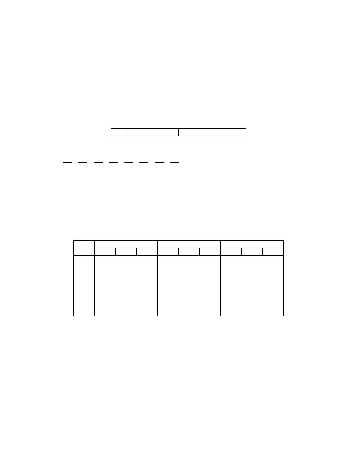
MOTOROLA INSTRUCTION SET DETAILS M68HC11
A-34 REFERENCE MANUAL
BSET Set Bit(s) in Memory BSET
Operation: M⇐(M)+ (PC + 2)
M⇐(M)+ (PC + 3) (for IND,Y address mode only)
Description: Set multiple bits in location M. The bit(s) to be set are specified by ones in
the mask byte (last machine code byte of the instruction). All other bits in M are
unaffected.
Condition Codes and Boolean Formulae:
NR7
Set if MSB of result is set; cleared otherwise.
ZR7 • R6 • R5 • R4 • R3 • R2 • R1 • R0
Set if result is $00; cleared otherwise.
V0
Cleared
Source Forms: BSET (opr) (msk)
Addressing Modes, Machine Code, and Cycle-by-Cycle Execution:
SXHINZVC
———— ∆∆0—
Cycle BSET (DIR) BSET (IND,X) BSET (IND,Y)
Addr Data R/W Addr Data R/W Addr Data R/W
1 OP 14 1 OP 1C 1 OP 18 1
2 OP+1 dd 1 OP+1 ff 1 OP+1 1C 1
3 00dd (00dd) 1 FFFF — 1 OP+2 ff 1
4 OP+2 mm 1 X+ff (X+ff) 1 FFFF — 1
5 FFFF — 1 OP+2 mm 1 (IY)+ff (Y+ff) 1
6 00dd result 0 FFFF — 1 OP+3 mm 1
7 X+ff result 0 FFFF — 1
8 Y+ff result 0

M68HC11 INSTRUCTION SET DETAILS MOTOROLA
REFERENCE MANUAL A-35
BSR Branch to Subroutine BSR
Operation: PC ⇐(PC)+ $0002 Advance PC to return address
⇓(PCL) Push low-order return onto stack
SP ⇐(SP) – $0001
⇓(PCH) Push high-order return onto stack
SP ⇐ (SP) – $0001
PC ⇐ (PC) + Rel Load start address of requested address
Description: The program counter is incremented by two (this will be the return address).
The least significant byte of the contents of the program counter (low-order return
address) is pushed onto the stack. The stack pointer is then decremented by one.
The most significant byte of the contents of the program counter (high-order return
address) is pushed onto the stack. The stack pointer is then decremented by one.
A branch then occurs to the location specified by the branch offset.
See BRA instruction for further details of the execution of the branch.
Condition Codes and Boolean Formulae:
None affected
Source Forms: BSR (rel)
Addressing Modes, Machine Code, and Cycle-by-Cycle Execution:
SXHINZVC
————————
Cycle BSR (REL)
Addr Data R/W
1OP8D1
2 OP+1 rr 1
3 FFFF — 1
4 Sub Nxt op 1
5 SP Rtn lo 0
6 SP–1 Rtn hi 0
MOTOROLA INSTRUCTION SET DETAILS M68HC11
A-36 REFERENCE MANUAL
BVC Branch if Overflow Clear BVC
Operation: PC ⇐(PC)+ $0002 + Rel if (V) = 0
Description: Tests the state of the V bit in the CCR and causes a branch if V is clear.
Used after an operation on two’s-complement binary values, this instruction will
cause a branch if there was NO overflow. That is, branch if the two’s-complement
result was valid.
See BRA instruction for further details of the execution of the branch.
Condition Codes and Boolean Formulae:
None affected
Source Forms: BVC (rel)
Addressing Modes, Machine Code, and Cycle-by-Cycle Execution:
The following table is a summary of all branch instructions.
SXHINZVC
————————
Cycle BVC (REL)
Addr Data R/W
1OP28 1
2 OP+1 rr 1
3 FFFF — 1
Test Boolean Mnemonic Opcode Complementary Branch Comment
r>m Z+(N⊕V)=0 BGT 2E r≤m BLE 2F Signed
r≥mN⊕V=0 BGE 2C r<m BLT 2D Signed
r=m Z=1 BEQ 27 r≠m BNE 26 Signed
r≤m Z+(N⊕V)=1 BLE 2F r>m BGT 2E Signed
r<m N⊕V=1 BLT 2D r≥m BGE 2C Signed
r>m C+Z=0 BHI 22 r≤m BLS 23 Unsigned
r≥m C=0 BHS/BCC 24 r<m BLO/BCS 25 Unsigned
r=m Z=1 BEQ 27 r≠m BNE 26 Unsigned
r≤m C+Z=1 BLS 23 r>m BHI 22 Unsigned
r<m C=1 BLO/BCS 25 r≥m BHS/BCC 24 Unsigned
Carry C=1 BCS 25 No Carry BCC 24 Simple
Negative N=1 BMI 2B Plus BPL 2A Simple
Overflow V=1 BVS 29 No Overflow BVC 28 Simple
r=0 Z=1 BEQ 27 r≠0 BNE 26 Simple
Always — BRA 20 Never BRN 21 Unconditional

M68HC11 INSTRUCTION SET DETAILS MOTOROLA
REFERENCE MANUAL A-37
BVS Branch if Overflow Set BVS
Operation: PC ⇐(PC)+ $0002 + Rel if (V) = 1
Description: Tests the state of the V bit in the CCR and causes a branch if V is set. Used
after an operation on two’s-complement binary values, this instruction will cause a
branch if there was an overflow. That is, branch if the two’s-complement result was
invalid.
See BRA instruction for further details of the execution of the branch.
Condition Codes and Boolean Formulae:
None affected
Source Forms: BVS (rel)
Addressing Modes, Machine Code, and Cycle-by-Cycle Execution:
The following table is a summary of all branch instructions.
SXHINZVC
————————
Cycle BVS (REL)
Addr Data R/W
1OP29 1
2 OP+1 rr 1
3 FFFF — 1
Test Boolean Mnemonic Opcode Complementary Branch Comment
r>m Z+(N⊕V)=0 BGT 2E r≤m BLE 2F Signed
r≥mN⊕V=0 BGE 2C r<m BLT 2D Signed
r=m Z=1 BEQ 27 r≠m BNE 26 Signed
r≤m Z+(N⊕V)=1 BLE 2F r>m BGT 2E Signed
r<m N⊕V=1 BLT 2D r≥m BGE 2C Signed
r>m C+Z=0 BHI 22 r≤m BLS 23 Unsigned
r≥m C=0 BHS/BCC 24 r<m BLO/BCS 25 Unsigned
r=m Z=1 BEQ 27 r≠m BNE 26 Unsigned
r≤m C+Z=1 BLS 23 r>m BHI 22 Unsigned
r<m C=1 BLO/BCS 25 r≥m BHS/BCC 24 Unsigned
Carry C=1 BCS 25 No Carry BCC 24 Simple
Negative N=1 BMI 2B Plus BPL 2A Simple
Overflow V=1 BVS 29 No Overflow BVC 28 Simple
r=0 Z=1 BEQ 27 r≠0 BNE 26 Simple
Always — BRA 20 Never BRN 21 Unconditional
MOTOROLA INSTRUCTION SET DETAILS M68HC11
A-38 REFERENCE MANUAL
CBA Compare Accumulators CBA
Operation: (ACCA) – (ACCB)
Description: Compares the contents of ACCA to the contents of ACCB and sets the con-
dition codes, which may be used for arithmetic and logical conditional branches.
Both operands are unaffected.
Condition Codes and Boolean Formulae:
NR7
Set if MSB of result is set; cleared otherwise.
ZR7 • R6 • R5 • R4 • R3 • R2 • R1 • R0
Set if result is $00; cleared otherwise.
V A7 • B7 • R7 + A7 • B7 • R7
Set if a two’s complement overflow resulted from the operation; cleared otherwise.
CA7 • B7 + B7 • R7 + R7 • A7
Set if there was a borrow from the MSB of the result; cleared otherwise.
Source Forms: CBA
Addressing Modes, Machine Code, and Cycle-by-Cycle Execution:
SXHINZVC
———— ∆∆∆∆
Cycle CBA (INH)
Addr Data R/W
1OP11 1
2 OP+1 — 1

M68HC11 INSTRUCTION SET DETAILS MOTOROLA
REFERENCE MANUAL A-39
CLC Clear Carry CLC
Operation: C bit ⇐ 0
Description: Clears the C bit in the CCR.
CLC may be used to set up the C bit prior to a shift or rotate instruction involving
the C bit.
Condition Codes and Boolean Formulae:
C0
Cleared
Source Forms: CLC
Addressing Modes, Machine Code, and Cycle-by-Cycle Execution:
SXHINZVC
——————— 0
Cycle CLC (INH)
Addr Data R/W
1OP0C1
2 OP+1 — 1
MOTOROLA INSTRUCTION SET DETAILS M68HC11
A-40 REFERENCE MANUAL
CLI Clear Interrupt Mask CLI
Operation: I bit ⇐ 0
Description: Clears the interrupt mask bit in the CCR. When the I bit is clear, interrupts
are enabled. There is one E-clock cycle delay in the clearing mechanism for the I
bit so that, if interrupts were previously disabled, the next instruction after a CLI will
always be executed, even if there was an interrupt pending prior to execution of the
CLI instruction.
Condition Codes and Boolean Formulae:
I0
Cleared
Source Forms: CLI
Addressing Modes, Machine Code, and Cycle-by-Cycle Execution:
SXHINZVC
——— 0 ————
Cycle CLI (INH)
Addr Data R/W
1OP0E1
2 OP+1 — 1
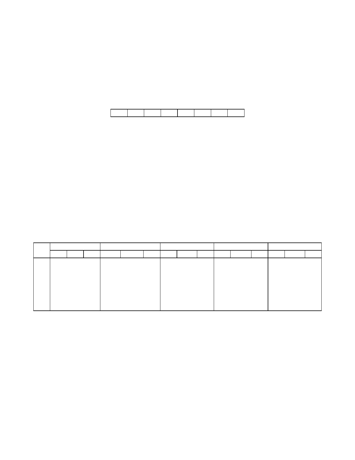
M68HC11 INSTRUCTION SET DETAILS MOTOROLA
REFERENCE MANUAL A-41
CLR Clear CLR
Operation: ACCX ⇐ 0 or: M⇐ 0
Description: The contents of ACCX or M are replaced with zeros.
Condition Codes and Boolean Formulae:
N0
Cleared
Z1
Set
V0
Cleared
C0
Cleared
Source Forms: CLRA; CLRB; CLR (opr)
Addressing Modes, Machine Code, and Cycle-by-Cycle Execution:
SXHINZVC
———— 0100
Cycle CLRA (IMM) CLRB (DIR) CLR (EXT) CLR (IND,X) CLR (IND,Y)
Addr Data R/W Addr Data R/W Addr Data R/W Addr Data R/W Addr Data R/W
1 OP 4F 1 OP 5F 1 OP 7F 1 OP 6F 1 OP 18 1
2 OP+1 — 1 OP+1 — 1 OP+1 hh 1 OP+1 ff 1 OP+1 6F 1
3 OP+2 ll 1 FFFF — 1 OP+2 ff 1
4 hhll (hhll) 1 X+ff (X+ff) 1 FFFF — 1
5 FFFF — 1 FFFF — 1 Y+ff (Y+ff) 1
6 hhll 00 0 X+ff 00 0 FFFF — 1
7 Y+ff 00 0

MOTOROLA INSTRUCTION SET DETAILS M68HC11
A-42 REFERENCE MANUAL
CLV Clear Two’s Complement Overflow Bit CLV
Operation: V bit ⇐ 0
Description: Clears the two’s complement overflow bit in the CCR.
Condition Codes and Boolean Formulae:
V0
Cleared
Source Forms: CLV
Addressing Modes, Machine Code, and Cycle-by-Cycle Execution:
SXHINZVC
—————— 0 —
Cycle CLV (INH)
Addr Data R/W
1OP0A1
2 OP+1 — 1
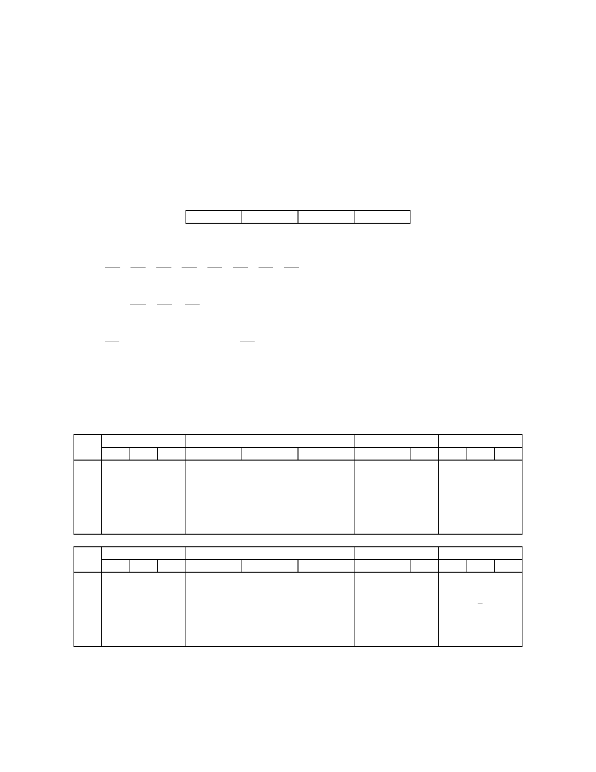
M68HC11 INSTRUCTION SET DETAILS MOTOROLA
REFERENCE MANUAL A-43
CMP Compare CMP
Operation: (ACCA) – (M)
Description: Compares the contents of ACCX to the contents of M and sets the condition
codes, which may be used for arithmetic and logical conditional branching. Both
operands are unaffected.
Condition Codes and Boolean Formulae:
NR7
Set if MSB of result is set; cleared otherwise.
ZR7 • R6 • R5 • R4 • R3 • R2 • R1 • R0
Set if result is $00; cleared otherwise.
V X7 • M7 • R7 + X7 • M7 • R7
Set if a two’s complement overflow resulted from the operation; cleared otherwise.
CX7 • M7 + M7 • R7 + R7 • X7
Set if there was a borrow from the MSB of the result; cleared otherwise.
Source Forms: CMPA (opr); CMPB (opr)
Addressing Modes, Machine Code, and Cycle-by-Cycle Execution:
SXHINZVC
———— ∆∆∆∆
Cycle CMPA(IMM) CMPA (DIR) CMPA (EXT) CMPA (IND,X) CMPA (IND,Y)
Addr Data R/W Addr Data R/W Addr Data R/W Addr Data R/W Addr Data R/W
1 OP 81 1 OP 91 1 OP B1 1 OP A1 1 OP 18 1
2 OP+1 ii 1 OP+1 dd 1 OP+1 hh 1 OP+1 ff 1 OP+1 A1 1
3 00dd (00dd
)1 OP+2 ll 1 FFFF — 1 OP+2 ff 1
4 hhll (hhll) 1 X+ff (X+ff) 1 FFFF — 1
5 Y+ff (Y+ff) 1
Cycle CMPB (IMM) CMPB (DIR) CMPB (EXT) CMPB (IND,X) CMPB (IND,Y)
Addr Data R/W Addr Data R/W Addr Data R/W Addr Data R/W Addr Data R/W
1 OP C1 1 OP D1 1 OP F1 1 OP E1 1 OP 18 1
2 OP+1 ii 1 OP+1 dd 1 OP+1 hh 1 OP+1 ff 1 OP+1 E1 1
3 00dd (00dd
)1 OP+2 ll 1 FFFF — 1 OP+2 ff 1
4 hhll (hhll) 1 X+ff (X+ff) 1 FFFF — 1
5 Y+ff (Y+ff) 1
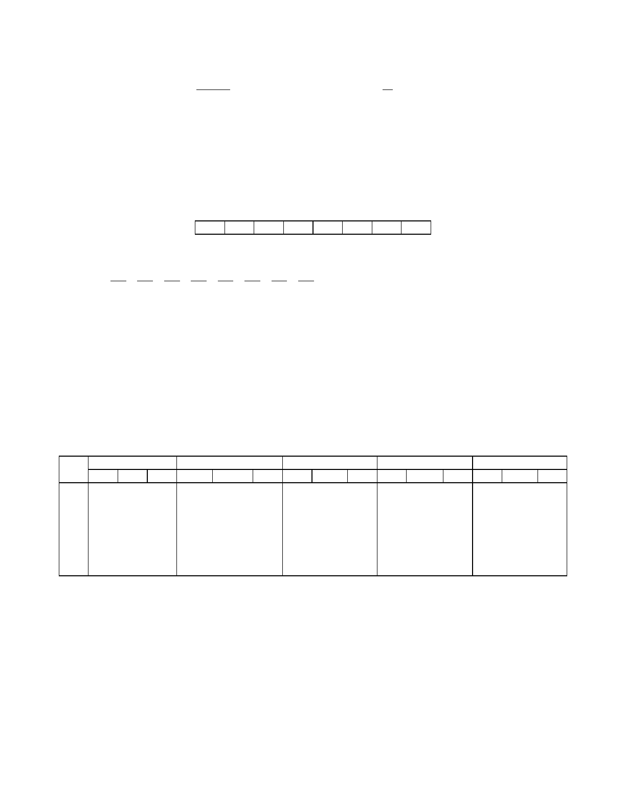
MOTOROLA INSTRUCTION SET DETAILS M68HC11
A-44 REFERENCE MANUAL
COM Complement COM
Operation: ACCX ⇐ (ACCX) + $FF – (ACCX) or: M ⇐ (M) + $FF – (M)
Description: Replaces the contents of ACCX or M with its one’s complement. (Each bit
of the contents of ACCX or M is replaced with the complement of that bit.) To com-
plement a value without affecting the C-bit, EXclusive-OR the value with $FF.
Condition Codes and Boolean Formulae:
NR7
Set if MSB of result is set; cleared otherwise.
ZR7 • R6 • R5 • R4 • R3 • R2 • R1 • R0
Set if result is $00; cleared otherwise.
V0
Cleared
C1
Set (For compatibility with M6800)
Source Forms: COMA; COMB; COM (opr)
Addressing Modes, Machine Code, and Cycle-by-Cycle Execution:
SXHINZVC
———— ∆∆01
Cycle COMA (INH) COMB (INH) COM (EXT) COM (IND,X) COM (IND,Y)
Addr Data R/W Addr Data R/W Addr Data R/W Addr Data R/W Addr Data R/W
1 OP 43 1 OP 53 1 OP 73 1 OP 63 1 OP 18 1
2 OP+1 — 1 OP+1 — 1 OP+1 hh 1 OP+1 ff 1 OP+1 63 1
3 OP+2 ll 1 FFFF — 1 OP+2 ff 1
4 hhll (hhll) 1 X+ff (X+ff) 1 FFFF — 1
5 FFFF — 1 FFFF — 1 Y+ff (Y+ff) 1
6 hhll result 0 X+ff result 0 FFFF — 1
7 Y+ff result 0
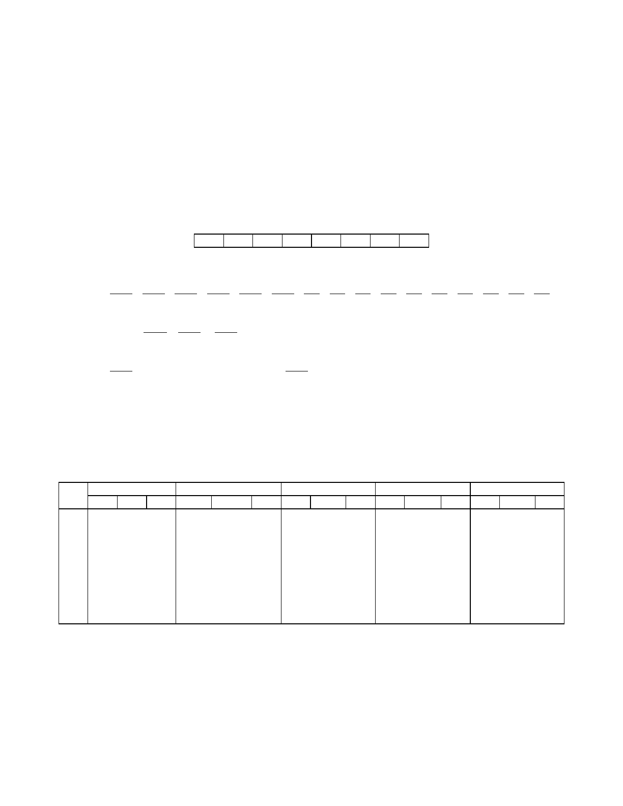
M68HC11 INSTRUCTION SET DETAILS MOTOROLA
REFERENCE MANUAL A-45
CPD Compare Double Accumulator CPD
Operation: (ACCD) – (M : M + 1)
Description: Compares the contents of accumulator D with a 16-bit value at the address
specified and sets the condition codes accordingly. The compare is accomplished
internally by doing a 16-bit subtract of (M:M+1)from accumulator D without mod-
ifying either accumulator D or (M : M + 1).
Condition Codes and Boolean Formulae:
N R15
Set if MSB of result is set; cleared otherwise.
ZR15 • R14 • R13 • R12 • R11 • R10 • R9 • R8 • R7 • R6 • R5 • R4 • R3 • R2 • R1 • R0
Set if result is $0000; cleared otherwise.
V D15 • M15 • R15 + D15 • M15 • R15
Set if a two’s complement overflow resulted from the operation; cleared otherwise.
CD15 • M15 + M15 • R15 + R15 • D15
Set if the absolute value of the contents of memory is larger than the absolute value
of the accumulator; cleared otherwise.
Source Forms: CPD (opr)
Addressing Modes, Machine Code, and Cycle-by-Cycle Execution:
SXHINZVC
———— ∆∆∆∆
Cycle CPD (IMM) CPD (DIR) CPD (EXT) CPD (IND,X) CPD (IND,Y)
Addr Data R/W Addr Data R/W Addr Data R/W Addr Data R/W Addr Data R/W
1 OP 1A 1 OP 1A 1 OP 1A 1 OP 1A 1 OP CD 1
2 OP+1 83 1 OP+1 93 1 OP+1 B3 1 OP+1 A3 1 OP+1 A3 1
3 OP+2 jj 1 OP+2 dd 1 OP+2 hh 1 OP+2 ff 1 OP+2 ff 1
4 OP+3 kk 1 00dd (00dd) 1 OP+3 ll 1 FFFF — 1 FFFF — 1
5 FFFF — 1 00dd+1 (00dd+1
)1 hhll (hhll) 1 X+ff (X+ff) 1 Y+ff (Y+ff) 1
6 FFFF — 1 hhll+1 (hhll+1) 1 X+ff+
1(X+ff+1
)1Y+ff+
1(Y+ff+1
)1
7 FFFF — 1 FFFF — 1 FFFF — 1
MOTOROLA INSTRUCTION SET DETAILS M68HC11
A-46 REFERENCE MANUAL
CPX Compare Index Register X CPX
Operation: (IX) – (M : M + 1)
Description: Compares the contents of index register X with a 16-bit value at the address
specified and sets the condition codes accordingly. The compare is accomplished
internally by doing a 16-bit subtract of (M : M + 1) from index register X without
modifying either index register X or (M : M + 1).
Condition Codes and Boolean Formulae:
N R15
Set if MSB of result is set; cleared otherwise.
ZR15 • R14 • R13 • R12 • R11 • R10 • R9 • R8 • R7 • R6 • R5 • R4 • R3 • R2 • R1 • R0
Set if result is $0000; cleared otherwise.
V IX15 • M15 • R15 + IX15 • M15 • R15
Set if a two’s complement overflow resulted from the operation; cleared otherwise.
CIX15 • M15 + M15 • R15 + R15 • IX15
Set if the absolute value of the contents of memory is larger than the absolute value
of the index register; cleared otherwise.
Source Forms: CPX (opr)
Addressing Modes, Machine Code, and Cycle-by-Cycle Execution:
SXHINZVC
———— ∆∆∆∆
Cycle CPX (IMM) CPX (DIR) CPX (EXT) CPX (IND,X) CPX (IND,Y)
Addr Data R/W Addr Data R/W Addr Data R/W Addr Data R/W Addr Data R/W
1 OP 8C 1 OP 9C 1 OP BC 1 OP AC 1 OP CD 1
2 OP+1 jj 1 OP+1 dd 1 OP+1 hh 1 OP+1 ff 1 OP+1 AC 1
3 OP+2 kk 1 00dd (00dd) 1 OP+2 hh 1 FFFF — 1 OP+2 ff 1
4 FFFF — 1 00dd+1 (00dd+1
)1 hhll (hhll) 1 X+ff (X+ff) 1 FFFF — 1
5 FFFF — 1 hhll+1 (hhll+1) 1 X+ff+
1(X+ff+1
)1 Y+ff (Y+ff) 1
6 FFFF — 1 FFFF — 1 Y+ff+
1(Y+ff+1
)1
7 FFFF — 1
M68HC11 INSTRUCTION SET DETAILS MOTOROLA
REFERENCE MANUAL A-47
CPY Compare Index Register Y CPY
Operation: (IY) – (M : M + 1)
Description: Compares the contents of index register Y with a 16-bit value at the address
specified and sets the condition codes accordingly. The compare is accomplished
internally by doing a 16-bit subtract of (M : M + 1) from index register Y without
modifying either index register Y or (M : M + 1).
Condition Codes and Boolean Formulae:
N R15
Set if MSB of result is set; cleared otherwise.
ZR15 • R14 • R13 • R12 • R11 • R10 • R9 • R8 • R7 • R6 • R5 • R4 • R3 • R2 • R1 • R0
Set if result is $0000; cleared otherwise.
V IY15 • M15 • R15 + IY15 • M15 • R15
Set if a two’s complement overflow resulted from the operation; cleared otherwise.
CIY15 • M15 + M15 • R15 + R15 • IY15
Set if the absolute value of the contents of memory is larger than the absolute value
of the index register; cleared otherwise.
Source Forms: CPY (opr)
Addressing Modes, Machine Code, and Cycle-by-Cycle Execution:
SXHINZVC
———— ∆∆∆∆
Cycle CPY (IMM) CPY (DIR) CPY (EXT) CPY (IND,X) CPY (IND,Y)
Addr Data R/W Addr Data R/W Addr Data R/W Addr Data R/W Addr Data R/W
1 OP 18 1 OP 18 1 OP 18 1 OP 1A 1 OP 18 1
2 OP+1 8C 1 OP+1 9C 1 OP+1 BC 1 OP+1 AC 1 OP+1 AC 1
3 OP+2 jj 1 OP+2 dd 1 OP+2 hh 1 OP+2 ff 1 OP+2 ff 1
4 OP+3 kk 1 00dd (00dd) 1 OP+3 ll 1 FFFF — 1 FFFF — 1
5 FFFF — 1 00dd+1 (00dd+1
)1 hhll (hhll) 1 X+ff (X+ff) 1 Y+ff (Y+ff) 1
6 FFFF — 1 hhll+1 (hhll+1) 1 X+ff+
1(X+ff+1
)1Y+ff+
1(Y+ff+1
)1
7 FFFF — 1 FFFF — 1 FFFF — 1
MOTOROLA INSTRUCTION SET DETAILS M68HC11
A-48 REFERENCE MANUAL
DAA Decimal Adjust Accumulator A DAA
Operation: The following table summarizes the operation of the DAA instruction for all le-
gal combinations of input operands. A correction factor (column 5 in the following
table) is added to ACCA to restore the result of an addition of two BCD operands
to a valid BCD value and set or clear the carry bit.
NOTE
Columns (1) through (4) of the above table represent all possible cas-
es which can result from any of the operations ABA, ADD, or ADC,
with initial carry either set or clear, applied to two binary-coded-dec-
imal operands. The table shows hexadecimal values.
Description: If the contents of ACCA and the state of the carry/borrow bit C and the state
of the half-carry bit H are all the result of applying any of the operations ABA, ADD,
or ADC to binary-coded-decimal operands, with or without an initial carry, the DAA
operation will adjust the contents of ACCA and the carry bit C in the CCR to repre-
sent the correct binary-coded-decimal sum and the correct state of the C bit.
Condition Codes and Boolean Formulae:
NR7
Set if MSB of result is set; cleared otherwise.
ZR7 • R6 • R5 • R4 • R3 • R2 • R1 • R0
Set if result is $00; cleared otherwise.
V?
Not defined
C See table above
State of C Bit
Before DAA
(Column 1)
Upper Half-Byte
of ACCA
(Bits [7:4])
(Column 2)
Initial Half-Carry
H Bit from CCR
(Column 3)
Lower Half-Byte
of ACCA
(Bits [3:0])
(Column 4)
Number Added
to ACCA by DAA
(Column 5)
State of C Bit
After DAA
(Column 6)
0 0-9 0 0-9 00 0
0 0-8 0 A-F 06 0
0 0-9 1 0-3 06 0
0 A-F 0 0-9 60 1
0 9-F 0 A-F 66 1
0 A-F 1 0-3 66 1
1 0-2 0 0-9 60 1
1 0-2 0 A-F 66 1
1 0-3 1 0-3 66 1
SXHINZVC
———— ∆∆?∆

M68HC11 INSTRUCTION SET DETAILS MOTOROLA
REFERENCE MANUAL A-49
DAA Decimal Adjust Accumulator A DAA
(Continued)
Source Forms: DAA
Addressing Modes, Machine Code, and Cycle-by-Cycle Execution:
For the purpose of illustration, consider the case where the BCD value $99 was just
added to the BCD value $22. The add instruction is a binary operation, which yields
the result $BB with no carry (C) or half carry (H). This corresponds to the fifth row of
the table on the previous page. The DAA instruction will therefore add the correction
factor $66 to the result of the addition, giving a result of $21 with the carry bit set. This
result corresponds to the BCD value $121, which is the expected BCD result.
Cycle DAA (INH)
Addr Data R/W
1OP19 1
2 OP+1 — 1
MOTOROLA INSTRUCTION SET DETAILS M68HC11
A-50 REFERENCE MANUAL
DEC Decrement DEC
Operation: ACCX ⇐(ACCX) – $01 or: M⇐(M) – $01
Description: Subtract one from the contents of ACCX or M.
The N, Z, and V bits in the CCR are set or cleared according to the results of the
operation. The C bit in the CCR is not affected by the operation, thus allowing the
DEC instruction to be used as a loop counter in multiple-precision computations.
When operating on unsigned values, only BEQ and BNE branches can be expect-
ed to perform consistently. When operating on two’s complement values, all signed
branches are available.
Condition Codes and Boolean Formulae:
NR7
Set if MSB of result is set; cleared otherwise.
ZR7 • R6 • R5 • R4 • R3 • R2 • R1 • R0
Set if result is $00; cleared otherwise.
V X7 • X6 • X5 • X4 • X3 • X2 • X1 • X0 = R7 • R6 • R5 • R4 • R3 • R2 • R1 • R0
Set if a two’s complement overflow resulted from the operation; cleared otherwise.
Source Forms: DECA; DECB; DEC (opr)
Addressing Modes, Machine Code, and Cycle-by-Cycle Execution:
SXHINZVC
———— ∆∆∆—
Cycle DECA (INH) DECB (INH) DEC (EXT) DEC (IND,X) DEC (IND,Y)
Addr Data R/W Addr Data R/W Addr Data R/W Addr Data R/W Addr Data R/W
1 OP 4A 1 OP 5A 1 OP 7A 1 OP 6A 1 OP 18 1
2 OP+1 — 1 OP+1 — 1 OP+1 hh 1 OP+1 ff 1 OP+1 6A 1
3 OP+2 ll 1 FFFF — 1 OP+2 ff 1
4 hhll (hhll) 1 X+ff (X+ff) 1 FFFF — 1
5 FFFF — 1 FFFF — 1 Y+ff (Y+ff) 1
6 hhll result 0 X+ff result 0 FFFF — 1
7 Y+ff result 1

M68HC11 INSTRUCTION SET DETAILS MOTOROLA
REFERENCE MANUAL A-51
DES Decrement Stack Pointer DES
Operation: SP ⇐ (SP) – $0001
Description: Subtract one from the stack pointer
Condition Codes and Boolean Formulae:
None affected
Source Forms: DES
Addressing Modes, Machine Code, and Cycle-by-Cycle Execution:
SXHINZVC
————————
Cycle DES (INH)
Addr Data R/W
1OP34 1
2 OP+1 — 1
3SP— 1

MOTOROLA INSTRUCTION SET DETAILS M68HC11
A-52 REFERENCE MANUAL
DEX Decrement Index Register X DEX
Operation: IX ⇐ (IX) – $0001
Description: Subtract one from index register X
Only the Z bit is set or cleared according to the result of this operation.
Condition Codes and Boolean Formulae:
ZR15 • R14 • R13 • R12 • R11 • R10 • R9 • R8 • R7 • R6 • R5 • R4 • R3 • R2 • R1 • R0
Set if result is $0000; cleared otherwise.
Source Forms: DEX
Addressing Modes, Machine Code, and Cycle-by-Cycle Execution:
SXHINZVC
————— ∆——
Cycle DEX (INH)
Addr Data R/W
1OP09 1
2 OP+1 — 1
3 FFFF — 1

M68HC11 INSTRUCTION SET DETAILS MOTOROLA
REFERENCE MANUAL A-53
DEY Decrement Index Register Y DEY
Operation: IY ⇐ (IY) – $0001
Description: Subtract one from index register Y
Only the Z bit is set or cleared according to the result of this operation.
Condition Codes and Boolean Formulae:
ZR15 • R14 • R13 • R12 • R11 • R10 • R9 • R8 • R7 • R6 • R5 • R4 • R3 • R2 • R1 • R0
Set if result is $0000; cleared otherwise.
Source Forms: DEY
Addressing Modes, Machine Code, and Cycle-by-Cycle Execution:
SXHINZVC
————— ∆——
Cycle DEY (INH)
Addr Data R/W
1OP18 1
2 OP+1 09 1
3 OP+2 — 1
4 FFFF — 1
MOTOROLA INSTRUCTION SET DETAILS M68HC11
A-54 REFERENCE MANUAL
EOR Exclusive OR EOR
Operation: (ACCX) ⇐ (ACCX) ⊕ (M)
Description: Performs the logical exclusive-OR between the contents of ACCX and the
contents of M and places the result in ACCX. (Each bit of ACCX after the operation
will be the logical exclusive-OR of the corresponding bits of M and ACCX before
the operation.)
Condition Codes and Boolean Formulae:
NR7
Set if MSB of result is set; cleared otherwise.
ZR7 • R6 • R5 • R4 • R3 • R2 • R1 • R0
Set if result is $00; cleared otherwise.
V0
Cleared
Source Forms: EORA (opr); EORB (opr)
Addressing Modes, Machine Code, and Cycle-by-Cycle Execution:
SXHINZVC
———— ∆∆0—
Cycle EORA(IMM) EORA (DIR) EORA (EXT) EORA (IND,X) EORA (IND,Y)
Addr Data R/W Addr Data R/W Addr Data R/W Addr Data R/W Addr Data R/W
1 OP 88 1 OP 98 1 OP B8 1 OP A8 1 OP 18 1
2 OP+1 ii 1 OP+1 dd 1 OP+1 hh 1 OP+1 ff 1 OP+1 A8 1
3 00dd (00dd
)1 OP+2 ll 1 FFFF — 1 OP+2 ff 1
4 hhll (hhll) 1 X+ff (X+ff) 1 FFFF — 1
5 Y+ff (Y+ff) 1
Cycle EORB (IMM) EORB (DIR) EORB (EXT) EORB (IND,X) EORB (IND,Y)
Addr Data R/W Addr Data R/W Addr Data R/W Addr Data R/W Addr Data R/W
1 OP C8 1 OP D8 1 OP F8 1 OP E8 1 OP 18 1
2 OP+1 ii 1 OP+1 dd 1 OP+1 hh 1 OP+1 ff 1 OP+1 E8 1
3 00dd (00dd
)1 OP+2 ll 1 FFFF — 1 OP+2 ff 1
4 hhll (hhll) 1 X+ff (X+ff) 1 FFFF — 1
5 Y+ff (Y+ff) 1
M68HC11 INSTRUCTION SET DETAILS MOTOROLA
REFERENCE MANUAL A-55
FDIV Fractional Divide FDIV
Operation: (ACCD)/(IX); IX ⇐ Quotient, ACCD ⇐ Remainder
Description: Performs an unsigned fractional divide of the 16-bit numerator in the D ac-
cumulator by the 16-bit denominator in the index register X and sets the condition
codes accordingly. The quotient is placed in the index register X, and the remain-
der is placed in the D accumulator. The radix point is assumed to be in the same
place for both the numerator and the denominator. The radix point is to the left of
bit 15 for the quotient. The numerator is assumed to be less than the denominator.
In the case of overflow (the denominator is less than or equal to the numerator) or
divide by zero, the quotient is set to $FFFF, and the remainder is indeterminate.
FDIV is equivalent to multiplying the numerator by 216 and then performing a 32
by 16-bit integer divide. The result is interpreted as a binary-weighted fraction,
which resulted from the division of a 16-bit integer by a larger 16-bit integer. A re-
sult of $0001 corresponds to 0.000015, and $FFFF corresponds to 0.99998. The
remainder of an IDIV instruction can be resolved into a binary-weighted fraction by
an FDIV instruction. The remainder of an FDIV instruction can be resolved into the
next 16-bits of binary-weighted fraction by another FDIV instruction.
Condition Codes and Boolean Formulae:
ZR15 • R14 • R13 • R12 • R11 • R10 • R9 • R8 • R7 • R6 • R5 • R4 • R3 • R2 • R1 • R0
Set if quotient is $0000; cleared otherwise.
V 1 if IX ≤ D
Set if denominator was less than or equal to the numerator; cleared otherwise.
ZIX15 • IX14 • IX13 • IX12 • IX11 • IX10 • IX9 • IX8 • IX7 • IX6 • IX5 • IX4 • IX3 • IX2
•IX1 • IX0
Set if denominator was $0000; cleared otherwise.
Source Forms: FDIV
Addressing Modes, Machine Code, and Cycle-by-Cycle Execution:
SXHINZVC
————— ∆∆∆
Cycle FDIV (INH)
Addr Data R/W
1OP03 1
2 OP+1 — 1
3-41 FFFF — 1
MOTOROLA INSTRUCTION SET DETAILS M68HC11
A-56 REFERENCE MANUAL
IDIV Integer Divide IDIV
Operation: (ACCD)/(IX); IX ⇐ Quotient, ACCD ⇐ Remainder
Description: Performs an unsigned integer divide of the 16-bit numerator in D accumu-
lator by the 16-bit denominator in index register X and sets the condition codes ac-
cordingly. The quotient is placed in index register X, and the remainder is placed
in the D accumulator. The radix point is assumed to be in the same place for both
the numerator and the denominator. The radix point is to the right of bit zero for the
quotient. In the case of divide by zero, the quotient is set to $FFFF, and the remain-
der is indeterminate.
Condition Codes and Boolean Formulae:
ZR15 • R14 • R13 • R12 • R11 • R10 • R9 • R8 • R7 • R6 • R5 • R4 • R3 • R2 • R1 • R0
Set if result is $0000; cleared otherwise.
V0
Cleared
CIX15 • IX14 • IX13 • IX12 • IX11 • IX10 • IX9 • IX8 • IX7 • IX6 • IX5 • IX4 • IX3 • IX2
•IX1 • IX0
Set if denominator was $0000; cleared otherwise.
Source Forms: IDIV
Addressing Modes, Machine Code, and Cycle-by-Cycle Execution:
SXHINZVC
————— ∆0∆
Cycle IDIV (INH)
Addr Data R/W
1OP02 1
2 OP+1 — 1
3-41 FFFF — 1
M68HC11 INSTRUCTION SET DETAILS MOTOROLA
REFERENCE MANUAL A-57
INC Increment INC
Operation: ACCX ⇐ (ACCX) + $01 or: M ⇐ (M) + $01
Description: Add one to the contents of ACCX or M.
The N, Z, and V bits in the CCR are set or cleared according to the results of the
operation. The C bit in the CCR is not affected by the operation, thus allowing the
INC instruction to be used as a loop counter in multiple-precision computations.
When operating on unsigned values, only BEQ and BNE branches can be expect-
ed to perform consistently. When operating on two’s-complement values, all
signed branches are available.
Condition Codes and Boolean Formulae:
NR7
Set is MSB of result is set; cleared otherwise.
ZR7 • R6 • R5 • R4 • R3 • R2 • R1 • R0
Set if result is $00; cleared otherwise.
VX7 • X6 • X5 • X4 • X3 • X2 • X1 • X0
Set if there is a two’s complement overflow as a result of the operation; cleared oth-
erwise. Two’s complement overflow occurs if and only if (ACCX) or (M) was $7F
before the operation.
Source Forms: INCA; INCB; INC (opr)
Addressing Modes, Machine Code, and Cycle-by-Cycle Execution:
SXHINZVC
———— ∆∆∆∇
Cycle INCA (INH) INCB (INH) INC (EXT) INC (IND,X) INC (IND,Y)
Addr Data R/W Addr Data R/W Addr Data R/W Addr Data R/W Addr Data R/W
1 OP 4C 1 OP 5C 1 OP 7C 1 OP 6C 1 OP 18 1
2 OP+1 — 1 OP+1 — 1 OP+1 hh 1 OP+1 ff 1 OP+1 6C 1
3 OP+2 ll 1 FFFF — 1 OP+2 ff 1
4 hhll (hhll) 1 X+ff (X+ff) 1 FFFF — 1
5 FFFF — 1 FFFF — 1 Y+ff (Y+ff) 1
6 hhll result 0 X+ff result 0 FFFF — 1
7 Y+ff result 1

MOTOROLA INSTRUCTION SET DETAILS M68HC11
A-58 REFERENCE MANUAL
INS Increment Stack Pointer INS
Operation: SP ⇐ (SP) + $0001
Description: Adds one to the stack pointer.
Condition Codes and Boolean Formulae:
None affected
Source Forms: INS
Addressing Modes, Machine Code, and Cycle-by-Cycle Execution:
SXHINZVC
————————
Cycle INS (INH)
Addr Data R/W
1OP31 1
2 OP+1 — 1
3SP— 1
M68HC11 INSTRUCTION SET DETAILS MOTOROLA
REFERENCE MANUAL A-59
INX Increment Index Register X INX
Operation: IX ⇐ (IX) + $0001
Description: Adds one to index register X.
Only the Z bit is set or cleared according to the result of this operation.
Condition Codes and Boolean Formulae:
ZR15 • R14 • R13 • R12 • R11 • R10 • R9 • R8 • R7 • R6 • R5 • R4 • R3 • R2 • R1 • R0
Set if result is $0000; cleared otherwise.
Source Forms: INX
Addressing Modes, Machine Code, and Cycle-by-Cycle Execution:
SXHINZVC
————— ∆——
Cycle INX (INH)
Addr Data R/W
1OP08 1
2 OP+1 — 1
3 FFFF — 1

MOTOROLA INSTRUCTION SET DETAILS M68HC11
A-60 REFERENCE MANUAL
INY Increment Index Register Y INY
Operation: IY ⇐ (IY) + $0001
Description: Adds one to index register Y.
Only the Z bit is set or cleared according to the result of this operation.
Condition Codes and Boolean Formulae:
ZR15 • R14 • R13 • R12 • R11 • R10 • R9 • R8 • R7 • R6 • R5 • R4 • R3 • R2 • R1 • R0
Set if result is $0000; cleared otherwise.
Source Forms: INY
Addressing Modes, Machine Code, and Cycle-by-Cycle Execution:
SXHINZVC
————— ∆——
Cycle INY (INH)
Addr Data R/W
1OP18 1
2 OP+1 08 1
3 OP+2 — 1
4 FFFF — 1
M68HC11 INSTRUCTION SET DETAILS MOTOROLA
REFERENCE MANUAL A-61
JMP Jump JMP
Operation: PC ⇐Effective Address
Description: A jump occurs to the instruction stored at the effective address. The effec-
tive address is obtained according to the rules for EXTended or INDexed address-
ing.
Condition Codes and Boolean Formulae:
None affected
Source Forms: JMP (opr)
Addressing Modes, Machine Code, and Cycle-by-Cycle Execution:
SXHINZVC
————————
Cycle JMP (EXT) JMP (IND,X) JMP (IND,Y)
Addr Data R/W Addr Data R/W Addr Data R/W
1 OP 7E 1 OP 6E 1 OP 18 1
2 OP+1 hh 1 OP+1 ff 1 OP+1 6E 1
3 OP+2 ll 1 FFFF — 1 OP+2 ff 1
4 FFFF — 1
MOTOROLA INSTRUCTION SET DETAILS M68HC11
A-62 REFERENCE MANUAL
JSR Jump to Subroutine JSR
Operation: PC ⇐ (PC) + $0003 (for EXTended or INDexed, Y addressing) or:
PC ⇐ (PC) + $0002 (for DIRect or INDexed, X addressing)
⇓(PCL) Push low-order return address onto stack
SP ⇐ (SP) – $0001
⇓(PCH) Push high-order return address onto stack
SP ⇐ (SP) – $0001
PC ⇐ Effective Addr Load Start address or requested subroutine
Description: The program counter is incremented by three or by two, depending on the
addressing mode, and is then pushed onto the stack, eight bits at a time, least sig-
nificant byte first. The stack pointer points to the next empty location in the stack.
A jump occurs to the instruction stored at the effective address. The effective ad-
dress is obtained according to the rules for EXTended, DIRect, or INDexed ad-
dressing.
Condition Codes and Boolean Formulae:
None affected
Source Forms: JSR (opr)
Addressing Modes, Machine Code, and Cycle-by-Cycle Execution:
SXHINZVC
————————
Cycle JSR (DIR) JSR (EXT) JSR (IND,X) JSR (IND,Y)
Addr Data R/W Addr Data R/W Addr Data R/W Addr Data R/W
1 OP 9D 1 OP BD 1 OP AD 1 OP 18 1
2 OP+1 dd 1 OP+1 hh 1 OP+1 ff 1 OP+1 AD 1
3 00dd (00dd
)1 OP+2 ll 1 FFFF — 1 OP+2 ff 1
4 SP Rtn lo 0 hhll (hhll) 1 X+ff (X+ff) 1 FFFF — 1
5 Sp–1 Rtn hi 0 SP Rtn lo 0 SP Rtn lo 0 Y+ff (Y+ff) 1
6 SP–1 Rtn hi 0 SP–1 Rtn hi 0 SP Rtn lo 0
7 SP–1 Rtn hi 0
M68HC11 INSTRUCTION SET DETAILS MOTOROLA
REFERENCE MANUAL A-63
LDA Load Accumulator LDA
Operation: ACCX ⇐(M)
Description: Loads the contents of memory into the 8-bit accumulator. The condition
codes are set according to the data.
Condition Codes and Boolean Formulae:
NR7
Set if MSB of result is set; cleared otherwise.
ZR7 • R6 • R5 • R4 • R3 • R2 • R1 • R0
Set if result is $00; cleared otherwise.
V0
Cleared
Source Forms: LDAA (opr); LDAB (opr)
Addressing Modes, Machine Code, and Cycle-by-Cycle Execution:
SXHINZVC
———— ∆∆0—
Cycle LDAA (IMM) LDAA (DIR) LDAA (EXT) LDAA (IND,X) LDAA (IND,Y)
Addr Data R/W Addr Data R/W Addr Data R/W Addr Data R/W Addr Data R/W
1 OP 86 1 OP 96 1 OP B6 1 OP A6 1 OP 18 1
2 OP+1 ii 1 OP+1 dd 1 OP+1 hh 1 OP+1 ff 1 OP+1 A6 1
3 00dd (00dd
)1 OP+2 ll 1 FFFF — 1 OP+2 ff 1
4 hhll (hhll) 1 X+ff (X+ff) 1 FFFF — 1
5 Y+ff (Y+ff) 1
Cycle LDAB (IMM) LDAB (DIR) LDAB (EXT) LDAB (IND,X) LDAB (IND,Y)
Addr Data R/W Addr Data R/W Addr Data R/W Addr Data R/W Addr Data R/W
1 OP C6 1 OP D6 1 OP F6 1 OP E6 1 OP 18 1
2 OP+1 ii 1 OP+1 dd 1 OP+1 hh 1 OP+1 ff 1 OP+1 E6 1
3 00dd (00dd
)1 OP+2 ll 1 FFFF — 1 OP+2 ff 1
4 hhll (hhll) 1 X+ff (X+ff) 1 FFFF — 1
5 Y+ff (Y+ff) 1

MOTOROLA INSTRUCTION SET DETAILS M68HC11
A-64 REFERENCE MANUAL
LDD Load Double Accumulator LDD
Operation: ACCX ⇐(M : M + 1); ACCA ⇐(M), ACCB ⇐(M + 1)
Description: Loads the contents of memory locations M andM+1into the double accu-
mulator D. The condition codes are set according to the data. The information from
location M is loaded into accumulator A, and the information from location M + 1 is
loaded into accumulator B.
Condition Codes and Boolean Formulae:
N R15
Set if MSB of result is set; cleared otherwise.
ZR15 • R14 • R13 • R12 • R11 • R10 • R9 • R8 • R7 • R6 • R5 • R4 • R3 • R2 • R1 • R0
Set if result is $0000; cleared otherwise.
V0
Cleared
Source Forms: LDD (opr)
Addressing Modes, Machine Code, and Cycle-by-Cycle Execution:
SXHINZVC
———— ∆∆0—
Cycle LDD (IMM) LDD (DIR) LDD (EXT) LDD (IND,X) LDD (IND,Y)
Addr Data R/W Addr Data R/W Addr Data R/W Addr Data R/W Addr Data R/W
1 OP CC 1 OP DC 1 OP FC 1 OP EC 1 OP 18 1
2 OP+1 ii 1 OP+1 dd 1 OP+1 hh 1 OP+1 ff 1 OP+1 EC 1
3 OP+2 kk 1 00dd (00dd) 1 OP+2 ll 1 FFFF — 1 OP+2 ff 1
400dd+
1(00dd+1
)1 hhll (hhll) 1 X+ff (X+ff) 1 FFFF — 1
5 hhll+1 (hhll+1) 1 X+ff+
1(X+ff+1
)1 Y+ff (Y+ff) 1
6Y+ff+
1(Y+ff+1
)1

M68HC11 INSTRUCTION SET DETAILS MOTOROLA
REFERENCE MANUAL A-65
LDS Load Stack Pointer LDS
Operation: SPH ⇐(M), SPL ⇐(M + 1)
Description: Loads the most significant byte of the stack pointer from the byte of memory
at the address specified by the program, and loads the least significant byte of the
stack pointer from the next byte of memory at one plus the address specified by
the program.
Condition Codes and Boolean Formulae:
N R15
Set if MSB of result is set; cleared otherwise.
ZR15 • R14 • R13 • R12 • R11 • R10 • R9 • R8 • R7 • R6 • R5 • R4 • R3 • R2 • R1 • R0
Set if result is $0000; cleared otherwise.
V0
Cleared
Source Forms: LDS (opr)
Addressing Modes, Machine Code, and Cycle-by-Cycle Execution:
SXHINZVC
———— ∆∆0—
Cycle LDS (IMM) LDS (DIR) LDS (EXT) LDS (IND,X) LDS (IND,Y)
Addr Data R/W Addr Data R/W Addr Data R/W Addr Data R/W Addr Data R/W
1 OP BE 1 OP 9E 1 OP EE 1 OP AE 1 OP 18 1
2 OP+1 jj 1 OP+1 dd 1 OP+1 hh 1 OP+1 ff 1 OP+1 AE 1
3 OP+2 kk 1 00dd (00dd) 1 OP+2 ll 1 FFFF — 1 OP+2 ff 1
400dd+
1(00dd+1
)1 hhll (hhll) 1 X+ff (X+ff) 1 FFFF — 1
5 hhll+1 (hhll+1) 1 X+ff+
1(X+ff+1
)1 Y+ff (Y+ff) 1
6Y+ff+
1(Y+ff+1
)1

MOTOROLA INSTRUCTION SET DETAILS M68HC11
A-66 REFERENCE MANUAL
LDX Load Index Register X LDX
Operation: IXH ⇐(M), IXL ⇐(M + 1)
Description: Loads the most significant byte of index register X from the byte of memory
at the address specified by the program, and loads the least significant byte of in-
dex register X from the next byte of memory at one plus the address specified by
the program.
Condition Codes and Boolean Formulae:
N R15
Set if MSB of result is set; cleared otherwise.
ZR15 • R14 • R13 • R12 • R11 • R10 • R9 • R8 • R7 • R6 • R5 • R4 • R3 • R2 • R1 • R0
Set if result is $0000; cleared otherwise.
V0
Cleared
Source Forms: LDX (opr)
Addressing Modes, Machine Code, and Cycle-by-Cycle Execution:
SXHINZVC
———— ∆∆0—
Cycle LDX (IMM) LDX (DIR) LDX (EXT) LDX (IND,X) LDX (IND,Y)
Addr Data R/W Addr Data R/W Addr Data R/W Addr Data R/W Addr Data R/W
1 OP CE 1 OP DE 1 OP FE 1 OP EE 1 OP CD 1
2 OP+1 jj 1 OP+1 dd 1 OP+1 hh 1 OP+1 ff 1 OP+1 EE 1
3 OP+2 kk 1 00dd (00dd) 1 OP+2 ll 1 FFFF — 1 OP+2 ff 1
400dd+
1(00dd+1
)1 hhll (hhll) 1 X+ff (X+ff) 1 FFFF — 1
5 hhll+1 (hhll+1) 1 X+ff+
1(X+ff+1
)1 Y+ff (Y+ff) 1
6Y+ff+
1(Y+ff+1
)1
M68HC11 INSTRUCTION SET DETAILS MOTOROLA
REFERENCE MANUAL A-67
LDY Load Index Register Y LDY
Operation: IYH ⇐(M), IYL ⇐(M + 1)
Description: Loads the most significant byte of index register Y from the byte of memory
at the address specified by the program, and loads the least significant byte of in-
dex register Y from the next byte of memory at one plus the address specified by
the program.
Condition Codes and Boolean Formulae:
N R15
Set if MSB of result is set; cleared otherwise.
ZR15 • R14 • R13 • R12 • R11 • R10 • R9 • R8 • R7 • R6 • R5 • R4 • R3 • R2 • R1 • R0
Set if result is $0000; cleared otherwise.
V0
Cleared
Source Forms: LDY (opr)
Addressing Modes, Machine Code, and Cycle-by-Cycle Execution:
SXHINZVC
———— ∆∆0—
Cycle LDY (IMM) LDY (DIR) LDY (EXT) LDY (IND,X) LDY (IND,Y)
Addr Data R/W Addr Data R/W Addr Data R/W Addr Data R/W Addr Data R/W
1 OP 18 1 OP 18 1 OP 18 1 OP 1A 1 OP 18 1
2 OP+1 CE 1 OP+1 DE 1 OP+1 FE 1 OP+1 EE 1 OP+1 EE 1
3 OP+2 jj 1 OP+2 dd 1 OP+2 hh 1 OP+2 ff 1 OP+2 ff 1
4 OP+3 kk 1 00dd (00dd) 1 OP+3 ll 1 FFFF — 1 FFFF — 1
500dd+
1(00dd+1
)1 hhll (hhll) 1 X+ff (X+ff) 1 Y+ff (Y+ff) 1
6 hhll+1 (hhll+1) 1 X+ff+
1(X+ff+1
)1Y+ff+
1(Y+ff+1
)1
MOTOROLA INSTRUCTION SET DETAILS M68HC11
A-68 REFERENCE MANUAL
LSL Logical Shift Left LSL
(Same as ASL)
Operation:
Description: Shifts all bits of the ACCX or M one place to the left. Bit 0 is loaded with a
zero. The C bit in the CCR is loaded from the most significant bit of ACCX or M.
Condition Codes and Boolean Formulae:
NR7
Set if MSB of result is set; cleared otherwise.
ZR7 • R6 • R5 • R4 • R3 • R2 • R1 • R0
Set if result is $00; cleared otherwise.
VN⊕C = [N • C] + [N • C] (for N and C after the shift)
Set if (N is set and C is clear) or (N is clear and C is set); cleared otherwise (for
values of N and C after the shift).
CM7
Set if, before the shift, the MSB of ACCX or M was set; cleared otherwise.
Source Forms: LSLA; LSLB; LSL (opr)
Addressing Modes, Machine Code, and Cycle-by-Cycle Execution:
SXHINZVC
———— ∆∆∆∆
Cycle LSLA (INH) LSLB (INH) LSL (EXT) LSL (IND,X) LSL (IND,Y)
Addr Data R/W Addr Data R/W Addr Data R/W Addr Data R/W Addr Data R/W
1 OP 48 1 OP 58 1 OP 78 1 OP 68 1 OP 18 1
2 OP+1 — 1 OP+1 — 1 OP+1 hh 1 OP+1 ff 1 OP+1 68 1
3 OP+2 ll 1 FFFF — 1 OP+2 ff 1
4 hhll (hhll) 1 X+ff (X+ff) 1 FFFF — 1
5 FFFF — 1 FFFF — 1 Y+ff (Y+ff) 1
6 hhll result 0 X+ff result 0 FFFF — 1
7 Y+ff result 0
Cb7 – – – – – – b0 0
M68HC11 INSTRUCTION SET DETAILS MOTOROLA
REFERENCE MANUAL A-69
LSLD Logical Shift Left Double LSLD
(Same as ASLD)
Operation:
Description: Shifts all bits of ACCD one place to the left. Bit 0 is loaded with a zero. The
C bit in the CCR is loaded from the most significant bit of ACCD.
Condition Codes and Boolean Formulae:
N R15
Set if MSB of result is set; cleared otherwise.
ZR15 • R14 • R13 • R12 • R11 • R10 • R9 • R8 • R7 • R6 • R5 • R4 • R3 • R2 • R1 • R0
Set if result is $0000; cleared otherwise.
VN⊕C = [N • C] + [N • C] (for N and C after the shift)
Set if (N is set and C is clear) or (N is clear and C is set); cleared otherwise (for
values of N and C after the shift).
C D15
Set if, before the shift, the MSB of ACCD was set; cleared otherwise.
Source Forms: LSLD (opr)
Addressing Modes, Machine Code, and Cycle-by-Cycle Execution:
SXHINZVC
———— ∆∆∆∆
Cycle LSLD (INH)
Addr Data R/W
1OP05 1
2 OP+1 — 1
3 FFFF — 1
C b7 – – – – – – b0 b7 – – – – – – b0 0
ACCA ACCB
MOTOROLA INSTRUCTION SET DETAILS M68HC11
A-70 REFERENCE MANUAL
LSR Logical Shift Right LSR
Operation:
Description: Shifts all bits of the ACCX or M one place to the right. Bit 7 is loaded with
zero. The C bit is loaded from the least significant bit of ACCX or M.
Condition Codes and Boolean Formulae:
N0
Cleared.
ZR7 • R6 • R5 • R4 • R3 • R2 • R1 • R0
Set if result is $00; cleared otherwise.
VN⊕C = [N • C] + [N • C] (for N and C after the shift)
Since N = 0, this simplifies to C (after the shift).
CM0
Set if, before the shift, the LSB of ACCX or M was set; cleared otherwise.
Source Forms: LSRA; LSRB; LSR (opr)
Addressing Modes, Machine Code, and Cycle-by-Cycle Execution:
SXHINZVC
———— 0∆∆∆
Cycle LSRA (INH) LSRB (INH) LSR (EXT) LSR (IND,X) LSR (IND,Y)
Addr Data R/W Addr Data R/W Addr Data R/W Addr Data R/W Addr Data R/W
1 OP 44 1 OP 54 1 OP 74 1 OP 64 1 OP 18 1
2 OP+1 — 1 OP+1 — 1 OP+1 hh 1 OP+1 ff 1 OP+1 64 1
3 OP+2 ll 1 FFFF — 1 OP+2 ff 1
4 hhll (hhll) 1 X+ff (X+ff) 1 FFFF — 1
5 FFFF — 1 FFFF — 1 Y+ff (Y+ff) 1
6 hhll result 0 X+ff result 0 FFFF — 1
7 Y+ff result 0
C
b7 – – – – – – b0
0
M68HC11 INSTRUCTION SET DETAILS MOTOROLA
REFERENCE MANUAL A-71
LSRD Logical Shift Right Double Accumulator LSRD
Operation:
Description: Shifts all bits of ACCD one place to the right. Bit 15 (MSB of ACCA) is load-
ed with zero. The C bit is loaded from the least significant bit of ACCD (LSB of AC-
CB).
Condition Codes and Boolean Formulae:
N0
Cleared.
ZR15 • R14 • R13 • R12 • R11 • R10 • R9 • R8 • R7 • R6 • R5 • R4 • R3 • R2 • R1 • R0
Set if result is $0000; cleared otherwise.
VD0
Set if, after the shift operation, C is set; cleared otherwise.
CD0
Set if, before the shift, the least significant bit of ACCD was set; cleared otherwise.
Source Forms: LSRD (opr)
Addressing Modes, Machine Code, and Cycle-by-Cycle Execution:
SXHINZVC
———— 0∆∆∆
Cycle LSRD (INH)
Addr Data R/W
1OP04 1
2 OP+1 — 1
3 FFFF — 1
C
b7 – – – – – – b0 b7 – – – – – – b0
ACCA ACCB
0

MOTOROLA INSTRUCTION SET DETAILS M68HC11
A-72 REFERENCE MANUAL
MUL Multiply Unsigned MUL
Operation: ACCD ⇐ (ACCA) × (ACCB)
Description: Multiplies the 8-bit unsigned binary value in accumulator A by the 8-bit un-
signed binary value in accumulator B to obtain a 16-bit unsigned result in the dou-
ble accumulator D. Unsigned multiply allows multiple-precision operations. The
carry flag allows rounding the most significant byte of the result through the se-
quence: MUL, ADCA #0.
Condition Codes and Boolean Formulae:
CR7
Set if bit 7 of the result (ACCB bit 7) is set; cleared otherwise.
Source Forms: MUL
Addressing Modes, Machine Code, and Cycle-by-Cycle Execution:
SXHINZVC
——————— ∆
Cycle MUL (INH)
Addr Data R/W
1OP3D1
2 OP+1 — 1
3–10 FFFF — 1
M68HC11 INSTRUCTION SET DETAILS MOTOROLA
REFERENCE MANUAL A-73
NEG Negate NEG
Operation: ACCX ⇐ – (ACCX) = $00 – (ACCX) or: M ⇐ – (M) = $00 – (M)
Description: Replaces the contents of ACCX or M with its two’s complement; the value
$80 is left unchanged
Condition Codes and Boolean Formulae:
NR7
Set if MSB of result is set; cleared otherwise.
ZR7 • R6 • R5 • R4 • R3 • R2 • R1 • R0
Set if result is $00; cleared otherwise.
V R7 • R6 • R5 • R4 • R3 • R2 • R1 • R0
Set if there is a two’s complement overflow from the implied subtraction from zero;
cleared otherwise. A two’s complement overflow will occur if and only if the con-
tents of ACCX or M is $80.
C R7 + R6 + R5 + R4 + R3 + R2 + R1 + R0
Set if there is a borrow in the implied subtraction from zero; cleared otherwise. The
C bit will be set in all cases except when the contents of ACCX or M is $00.
Source Forms: NEGA; NEGB; NEG (opr)
Addressing Modes, Machine Code, and Cycle-by-Cycle Execution:
SXHINZVC
———— ∆∆∆∆
Cycle NEGA (INH) NEGB (INH) NEG (EXT) NEG (IND,X) NEG (IND,Y)
Addr Data R/W Addr Data R/W Addr Data R/W Addr Data R/W Addr Data R/W
1 OP 40 1 OP 50 1 OP 70 1 OP 60 1 OP 18 1
2 OP+1 — 1 OP+1 — 1 OP+1 hh 1 OP+1 ff 1 OP+1 60 1
3 OP+2 ll 1 FFFF — 1 OP+2 ff 1
4 hhll (hhll) 1 X+ff (X+ff) 1 FFFF — 1
5 FFFF — 1 FFFF — 1 Y+ff (Y+ff) 1
6 hhll result 0 X+ff result 0 FFFF — 1
7 Y+ff result 0

MOTOROLA INSTRUCTION SET DETAILS M68HC11
A-74 REFERENCE MANUAL
NOP No Operation NOP
Description: This is a single-byte instruction that causes only the program counter to be
incremented. No other registers are affected. This instruction is typically used to
produce a time delay although some software disciplines discourage CPU frequen-
cy-based time delays. During debug, NOP instructions are sometimes used to tem-
porarily replace other machine code instructions, thus disabling the replaced
instructions.
Condition Codes and Boolean Formulae:
None affected
Source Forms: NOP
Addressing Modes, Machine Code, and Cycle-by-Cycle Execution:
SXHINZVC
————————
Cycle NOP (INH)
Addr Data R/W
1OP01 1
2 OP+1 — 1

M68HC11 INSTRUCTION SET DETAILS MOTOROLA
REFERENCE MANUAL A-75
ORA Inclusive OR ORA
Operation: (ACCX) ⇐ (ACCX) + (M)
Description: Performs the logical inclusive-OR between the contents of ACCX and the
contents of M and places the result in ACCX. (Each bit of ACCX after the operation
will be the logical inclusive-OR of the corresponding bits of M and ACCX before the
operation.)
Condition Codes and Boolean Formulae:
NR7
Set if MSB of result is set; cleared otherwise.
ZR7 • R6 • R5 • R4 • R3 • R2 • R1 • R0
Set if result is $00; cleared otherwise.
V0
Cleared
Source Forms: ORAA (opr); ORAB (opr)
Addressing Modes, Machine Code, and Cycle-by-Cycle Execution:
SXHINZVC
———— ∆∆0—
Cycle ORAA (IMM) ORAA (DIR) ORAA (EXT) ORAA (IND,X) ORAA (IND,Y)
Addr Data R/W Addr Data R/W Addr Data R/W Addr Data R/W Addr Data R/W
1 OP 8A 1 OP 9A 1 OP BA 1 OP AA 1 OP 18 1
2 OP+1 ii 1 OP+1 dd 1 OP+1 hh 1 OP+1 ff 1 OP+1 AA 1
3 00dd (00dd
)1 OP+2 ll 1 FFFF — 1 OP+2 ff 1
4 hhll (hhll) 1 X+ff (X+ff) 1 FFFF — 1
5 Y+ff (Y+ff) 1
Cycle ORAB (IMM) ORAB (DIR) ORAB (EXT) ORAB (IND,X) ORAB (IND,Y)
Addr Data R/W Addr Data R/W Addr Data R/W Addr Data R/W Addr Data R/W
1 OP CA 1 OP DA 1 OP FA 1 OP EA 1 OP 18 1
2 OP+1 ii 1 OP+1 dd 1 OP+1 hh 1 OP+1 ff 1 OP+1 EA 1
3 00dd (00dd
)1 OP+2 ll 1 FFFF — 1 OP+2 ff 1
4 hhll (hhll) 1 X+ff (X+ff) 1 FFFF — 1
5 Y+ff (Y+ff) 1
MOTOROLA INSTRUCTION SET DETAILS M68HC11
A-76 REFERENCE MANUAL
PSH Push Data onto Stack PSH
Operation: ⇓ACCX, SP ⇐ (SP) – $0001
Description: The contents of ACCX are stored on the stack at the address contained in
the stack pointer. The stack pointer is then decremented.
Push instructions are commonly used to save the contents of one or more CPU
registers at the start of a subroutine. Just before returning from the subroutine, cor-
responding pull instructions are used to restore the saved CPU registers so the
subroutine will appear not to have affected these registers.
Condition Codes and Boolean Formulae:
None affected
Source Forms: PSHA; PSHB;
Addressing Modes, Machine Code, and Cycle-by-Cycle Execution:
SXHINZVC
————————
Cycle PSHA (INH) PSHB (INH)
Addr Data R/W Addr Data R/W
1 OP 36 1 OP 37 1
2 OP+1 — 1 OP+1 — 1
3 SP (A) 0 SP (B) 0

M68HC11 INSTRUCTION SET DETAILS MOTOROLA
REFERENCE MANUAL A-77
PSHX Push Index Register X onto Stack PSHX
Operation: ⇓(IXL), SP ⇐ (SP) – $0001
⇓(IXH), SP ⇐ (SP) – $0001
Description: The contents of index register X are pushed onto the stack (low-order byte
first) at the address contained in the stack pointer. The stack pointer is then decre-
mented by two.
Push instructions are commonly used to save the contents of one or more CPU
registers at the start of a subroutine. Just before returning from the subroutine, cor-
responding pull instructions are used to restore the saved CPU registers so the
subroutine will appear not to have affected these registers.
Condition Codes and Boolean Formulae:
None affected
Source Forms: PSHX
Addressing Modes, Machine Code, and Cycle-by-Cycle Execution:
SXHINZVC
————————
Cycle PSHX (INH)
Addr Data R/W
1OP3C1
2 OP+1 — 1
3 SP (IXL) 0
4 SP–1 (IXH) 0

MOTOROLA INSTRUCTION SET DETAILS M68HC11
A-78 REFERENCE MANUAL
PSHY Push Index Register Y onto Stack PSHY
Operation: ⇓(IYL), SP ⇐ (SP) – $0001
⇓(IYH), SP ⇐ (SP) – $0001
Description: The contents of index register Y are pushed onto the stack (low-order byte
first) at the address contained in the stack pointer. The stack pointer is then decre-
mented by two.
Push instructions are commonly used to save the contents of one or more CPU
registers at the start of a subroutine. Just before returning from the subroutine, cor-
responding pull instructions are used to restore the saved CPU registers so the
subroutine will appear not to have affected these registers.
Condition Codes and Boolean Formulae:
None affected
Source Forms: PSHY
Addressing Modes, Machine Code, and Cycle-by-Cycle Execution:
SXHINZVC
————————
Cycle PSHY (INH)
Addr Data R/W
1OP18 1
2 OP+1 3C 1
3 OP+2 — 1
4 SP (IYL) 0
5 SP–1 (IYH) 0

M68HC11 INSTRUCTION SET DETAILS MOTOROLA
REFERENCE MANUAL A-79
PUL Pull Data from Stack PUL
Operation: SP ⇐ (SP) + $0001, ⇑ACCX
Description: The stack pointer is incremented. The ACCX is then loaded from the stack
at the address contained in the stack pointer.
Push instructions are commonly used to save the contents of one or more CPU
registers at the start of a subroutine. Just before returning from the subroutine, cor-
responding pull instructions are used to restore the saved CPU registers so the
subroutine will appear not to have affected these registers.
Condition Codes and Boolean Formulae:
None affected
Source Forms: PULA; PULB;
Addressing Modes, Machine Code, and Cycle-by-Cycle Execution:
SXHINZVC
————————
Cycle PULA (INH) PULB (INH)
Addr Data R/W Addr Data R/W
1 OP 32 1 OP 33 1
2 OP+1 — 1 OP+1 — 1
3SP— 1 SP — 1
4 SP+1 get A 1 SP+1 get B 1

MOTOROLA INSTRUCTION SET DETAILS M68HC11
A-80 REFERENCE MANUAL
PULX Pull Index Register X from Stack PULX
Operation: SP ⇐ (SP) + $0001; ⇑(IXH)
SP ⇐ (SP) + $0001; ⇑(IXL)
Description: Index register X is pulled from the stack (high-order byte first) beginning at
the address contained in the stack pointer plus one. The stack pointer is increment-
ed by two in total.
Push instructions are commonly used to save the contents of one or more CPU
registers at the start of a subroutine. Just before returning from the subroutine, cor-
responding pull instructions are used to restore the saved CPU registers so the
subroutine will appear not to have affected these registers.
Condition Codes and Boolean Formulae:
None affected
Source Forms: PULX
Addressing Modes, Machine Code, and Cycle-by-Cycle Execution:
SXHINZVC
————————
Cycle PULX (INH)
Addr Data R/W
1OP38 1
2 OP+1 — 1
3SP— 1
4 SP+1 get IXH 1
5 SP+2 get IXL 1

M68HC11 INSTRUCTION SET DETAILS MOTOROLA
REFERENCE MANUAL A-81
PULY Pull Index Register Y from Stack PULY
Operation: SP ⇐ (SP) + $0001; ⇑(IYH)
SP ⇐ (SP) + $0001; ⇑(IYL)
Description: Index register Y is pulled from the stack (high-order byte first) beginning at
the address contained in the stack pointer plus one. The stack pointer is increment-
ed by two in total.
Push instructions are commonly used to save the contents of one or more CPU
registers at the start of a subroutine. Just before returning from the subroutine, cor-
responding pull instructions are used to restore the saved CPU registers so the
subroutine will appear not to have affected these registers.
Condition Codes and Boolean Formulae:
None affected
Source Forms: PULY
Addressing Modes, Machine Code, and Cycle-by-Cycle Execution:
SXHINZVC
————————
Cycle PULY (INH)
Addr Data R/W
1OP18 1
2 OP+1 38 1
3 OP+2 — 1
4SP— 1
5 SP+1 get IYH 1
6 SP+2 get IYL 1
MOTOROLA INSTRUCTION SET DETAILS M68HC11
A-82 REFERENCE MANUAL
ROL Rotate Left ROL
Operation:
Description: Shifts all bits of the ACCX or M one place to the left. Bit 0 is loaded from the
C bit. The C bit in the CCR is loaded from the most significant bit of ACCX or M.
The rotate operations include the carry bit to allow extension of the shift and rotate
operations to multiple bytes. For example, to shift a 24-bit value left one bit, the se-
quence ASL LOW, ROL MID, ROL HIGH could be used where LOW, MID, and
HIGH refer to the low-order, middle, and high-order bytes of the 24-bit value, re-
spectively.
Condition Codes and Boolean Formulae:
NR7
Set if MSB of result is set; cleared otherwise.
ZR7 • R6 • R5 • R4 • R3 • R2 • R1 • R0
Set if result is $00; cleared otherwise.
VN⊕C = [N • C] + [N • C] (for N and C after the rotate)
Set if (N is set and C is clear) or (N is clear and C is set); cleared otherwise (for
values of N and C after the rotate).
CM7
Set if, before the rotate, the MSB of ACCX or M was set; cleared otherwise.
Source Forms: ROLA; ROLB; ROL (opr)
Addressing Modes, Machine Code, and Cycle-by-Cycle Execution:
SXHINZVC
———— ∆∆∆∆
Cycle ROLA (INH) ROLB (INH) ROL (EXT) ROL (IND,X) ROL (IND,Y)
Addr Data R/W Addr Data R/W Addr Data R/W Addr Data R/W Addr Data R/W
1 OP 49 1 OP 59 1 OP 79 1 OP 69 1 OP 18 1
2 OP+1 — 1 OP+1 — 1 OP+1 hh 1 OP+1 ff 1 OP+1 69 1
3 OP+2 ll 1 FFFF — 1 OP+2 ff 1
4 hhll (hhll) 1 X+ff (X+ff) 1 FFFF — 1
5 FFFF — 1 FFFF — 1 Y+ff (Y+ff) 1
6 hhll result 0 X+ff result 0 FFFF — 1
7 Y+ff result 0
M68HC11 INSTRUCTION SET DETAILS MOTOROLA
REFERENCE MANUAL A-83
ROR Rotate Right ROR
Operation:
Description: Shifts all bits of the ACCX or M one place to the right. Bit 7 is loaded from
the C bit. The C bit in the CCR is loaded from the least significant bit of ACCX or
M. The rotate operations include the carry bit to allow extension of the shift and ro-
tate operations to multiple bytes. For example, to shift a 24-bit value right one bit,
the sequence LSR HIGH, ROR MID, ROR LOW could be used where LOW, MID,
and HIGH refer to the low-order, middle, and high-order bytes of the 24-bit value,
respectively. The first LSR could be replaced by ASR to maintain the original value
of the sign bit (MSB of high-order byte) of the 24-bit value.
Condition Codes and Boolean Formulae:
NR7
Set if MSB of result is set; cleared otherwise.
ZR7 • R6 • R5 • R4 • R3 • R2 • R1 • R0
Set if result is $00; cleared otherwise.
VN⊕C = [N • C] + [N • C] (for N and C after the rotate)
Set if (N is set and C is clear) or (N is clear and C is set); cleared otherwise (for
values of N and C after the rotate).
CM0
Set if, before the rotate, the LSB of ACCX or M was set; cleared otherwise.
Source Forms: RORA; RORB; ROR (opr)
Addressing Modes, Machine Code, and Cycle-by-Cycle Execution:
SXHINZVC
———— ∆∆∆∆
Cycle RORA (INH) RORB (INH) ROR (EXT) ROR (IND,X) ROR (IND,Y)
Addr Data R/W Addr Data R/W Addr Data R/W Addr Data R/W Addr Data R/W
1 OP 46 1 OP 56 1 OP 76 1 OP 66 1 OP 18 1
2 OP+1 — 1 OP+1 — 1 OP+1 hh 1 OP+1 ff 1 OP+1 66 1
3 OP+2 ll 1 FFFF — 1 OP+2 ff 1
4 hhll (hhll) 1 X+ff (X+ff) 1 FFFF — 1
5 FFFF — 1 FFFF — 1 Y+ff (Y+ff) 1
6 hhll result 0 X+ff result 0 FFFF — 1
7 Y+ff result 0

MOTOROLA INSTRUCTION SET DETAILS M68HC11
A-84 REFERENCE MANUAL
RTI Return from Interrupt RTI
Operation: SP⇐(SP)+ $0001, ⇑ (CCR)
SP⇐(SP)+ $0001, ⇑ (ACCB)
SP⇐(SP)+ $0001, ⇑ (ACCA)
SP⇐(SP)+ $0001, ⇑ (IXH)
SP⇐(SP)+ $0001, ⇑ (IXL)
SP⇐(SP)+ $0001, ⇑ (IYH)
SP⇐(SP)+ $0001, ⇑ (IYL)
SP⇐(SP)+ $0001, ⇑ (PCH)
SP⇐(SP)+ $0001, ⇑ (PCL)
Description: The condition code, accumulators B and A, index registers X and Y, and the
program counter will be restored to a state pulled from the stack. The X bit in the
CCR may be cleared as a result of an RTI instruction but may not be set if it was
cleared prior to execution of the RTI instruction.
Condition Codes and Boolean Formulae:
Condition code bits take on the value of the corresponding bit of the unstacked
CCR except that the X bit may not change from a zero to a one. Software can leave
X set, leave X clear, or change X from one to zero. The XIRQ interrupt mask can
only become set as a result of a RESET or recognition of an XIRQ interrupt.
Source Forms: RTI
Addressing Modes, Machine Code, and Cycle-by-Cycle Execution:
SXHINZVC
∆⇓∆∆∆∆∆∆
Cycle RTI (INH)
Addr Data R/W
1OP3B1
2 OP+1 — 1
3SP— 1
4 SP+1 get CC 1
5 SP+2 get B 1
6 SP+3 get A 1
7 SP+4 get IXH 1
8 SP+5 get IXL 1
9 SP+6 get IYH 1
10 SP+7 get IYL 1
11 SP+8 Rtn hi 1
12 SP+9 Rtn lo 1

M68HC11 INSTRUCTION SET DETAILS MOTOROLA
REFERENCE MANUAL A-85
RTS Return from Subroutine RTS
Operation: SP⇐(SP)+ $0001, ⇑ (PCH)
SP⇐(SP)+ $0001, ⇑ (PCL)
Description: The stack pointer is incremented by one. The contents of the byte of mem-
ory, at the address now contained in the stack pointer, are loaded into the high-or-
der eight bits of the program counter. The stack pointer is again incremented by
one. The contents of the byte of memory, at the address now contained in the stack
pointer, are loaded into the low-order eight bits of the program counter.
Condition Codes and Boolean Formulae:
None affected
Source Forms: RTS
Addressing Modes, Machine Code, and Cycle-by-Cycle Execution:
SXHINZVC
————————
Cycle RTS (INH)
Addr Data R/W
1OP39 1
2 OP+1 — 1
3SP— 1
4 SP+1 Rtn hi 1
5 SP+2 Rtn lo 1
MOTOROLA INSTRUCTION SET DETAILS M68HC11
A-86 REFERENCE MANUAL
SBA Subtract Accumulators SBA
Operation: ACCA ⇐(ACCA) – (ACCB)
Description: Subtracts the contents of ACCB from the contents of ACCA and places the
result in ACCA. The contents of ACCB are not affected. For subtract instructions,
the C bit in the CCR represents a borrow.
Condition Codes and Boolean Formulae:
NR7
Set if MSB of result is set; cleared otherwise.
ZR7 • R6 • R5 • R4 • R3 • R2 • R1 • R0
Set if result is $00; cleared otherwise.
V A7 • B7 • R7 + A7 • B7 • R7
Set if a two’s complement overflow resulted from the operation; cleared otherwise.
CA7 • B7 + B7 • R7 + R7 • A7
Set if the absolute value of ACCB is larger than the absolute value of ACCA;
cleared otherwise.
Source Forms: SBA
Addressing Modes, Machine Code, and Cycle-by-Cycle Execution:
SXHINZVC
———— ∆∆∆∆
Cycle SBA (INH)
Addr Data R/W
1OP10 1
2 OP+1 — 1
M68HC11 INSTRUCTION SET DETAILS MOTOROLA
REFERENCE MANUAL A-87
SBC Subtract with Carry SBC
Operation: ACCX ⇐(ACCA) – (M) – (C)
Description: Subtracts the contents of M and the contents of C from the contents of
ACCX and places the result in ACCX. For subtract instructions the C bit in the CCR
represents a borrow.
Condition Codes and Boolean Formulae:
NR7
Set if MSB of result is set; cleared otherwise.
ZR7 • R6 • R5 • R4 • R3 • R2 • R1 • R0
Set if result is $00; cleared otherwise.
V X7 • M7 • R7 + X7 • M7 • R7
Set if a two’s complement overflow resulted from the operation; cleared otherwise.
CX7 • M7 + M7 • R7 + R7 • X7
Set if the absolute value of the contents of memory plus previous carry is larger
than the absolute value of the accumulator; cleared otherwise.
Source Forms: SBCA (opr); SBCB (opr)
Addressing Modes, Machine Code, and Cycle-by-Cycle Execution:
SXHINZVC
———— ∆∆∆∆
Cycle SBCA (IMM) SBCA (DIR) SBCA (EXT) SBCA (IND,X) SBCA (IND,Y)
Addr Data R/W Addr Data R/W Addr Data R/W Addr Data R/W Addr Data R/W
1 OP 82 1 OP 92 1 OP B2 1 OP A2 1 OP 18 1
2 OP+1 ii 1 OP+1 dd 1 OP+1 hh 1 OP+1 ff 1 OP+1 A2 1
3 00dd (00dd
)1 OP+2 ll 1 FFFF — 1 OP+2 ff 1
4 hhll (hhll) 1 X+ff (X+ff) 1 FFFF — 1
5 Y+ff (Y+ff) 1
Cycle SBCB (IMM) SBCB (DIR) SBCB (EXT) SBCB (IND,X) SBCB (IND,Y)
Addr Data R/W Addr Data R/W Addr Data R/W Addr Data R/W Addr Data R/W
1 OP C2 1 OP D2 1 OP F2 1 OP E2 1 OP 18 1
2 OP+1 ii 1 OP+1 dd 1 OP+1 hh 1 OP+1 ff 1 OP+1 E2 1
3 00dd (00dd
)1 OP+2 ll 1 FFFF — 1 OP+2 ff 1
4 hhll (hhll) 1 X+ff (X+ff) 1 FFFF — 1
5 Y+ff (Y+ff) 1
MOTOROLA INSTRUCTION SET DETAILS M68HC11
A-88 REFERENCE MANUAL
SEC Set Carry SEC
Operation: C bit ⇐ 1
Description: Sets the C bit in the CCR.
Condition Codes and Boolean Formulae:
C1
Set
Source Forms: SEC
Addressing Modes, Machine Code, and Cycle-by-Cycle Execution:
SXHINZVC
——————— 1
Cycle SEC (INH)
Addr Data R/W
1OP0D1
2 OP+1 — 1
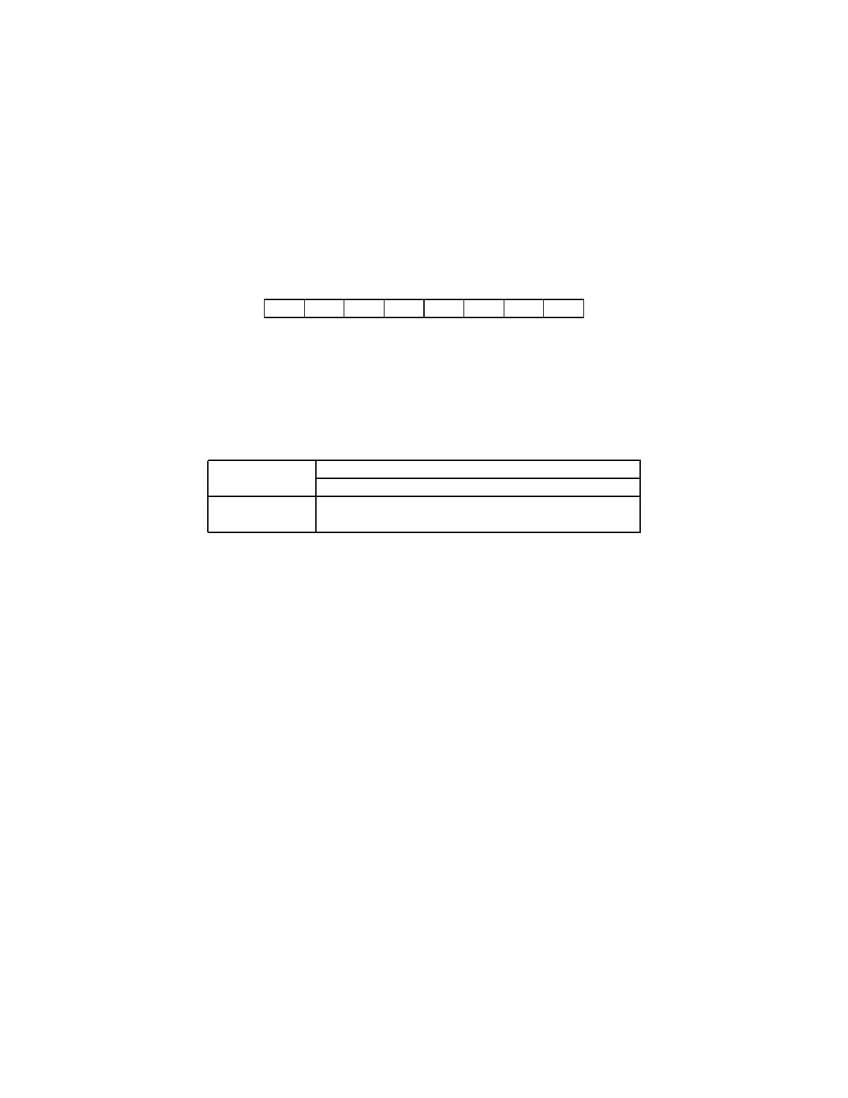
M68HC11 INSTRUCTION SET DETAILS MOTOROLA
REFERENCE MANUAL A-89
SEI Set Interrupt Mask SEI
Operation: I bit ⇐ 1
Description: Sets the interrupt mask bit in the CCR. When the I bet is set, all maskable
interrupts are inhibited, and the MPU will recognize only non-maskable interrupt
sources or an SWI.
Condition Codes and Boolean Formulae:
I1
Set
Source Forms: SEI
Addressing Modes, Machine Code, and Cycle-by-Cycle Execution:
SXHINZVC
——— 1 ————
Cycle SEI (INH)
Addr Data R/W
1OP0F 1
2 OP+1 — 1

MOTOROLA INSTRUCTION SET DETAILS M68HC11
A-90 REFERENCE MANUAL
SEV Set Two’s Complement Overflow Bit SEV
Operation: V bit ⇐ 1
Description: Sets the interrupt mask bit in the CCR. When the I bet is set, all maskable
interrupts are inhibited, and the MPU will recognize only non-maskable interrupt
sources or an SWI.
Condition Codes and Boolean Formulae:
V1
Set
Source Forms: SEV
Addressing Modes, Machine Code, and Cycle-by-Cycle Execution:
SXHINZVC
—————— 1 —
Cycle SEV (INH)
Addr Data R/W
1OP0B1
2 OP+1 — 1
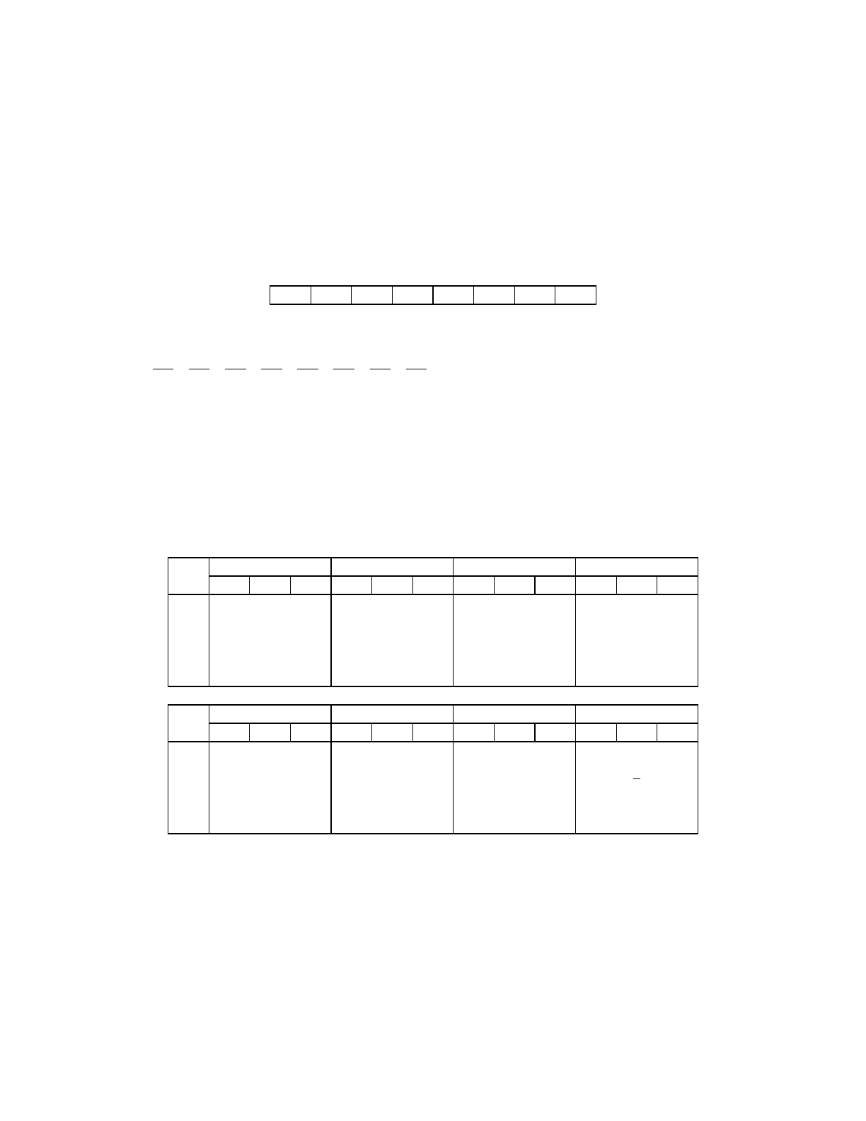
M68HC11 INSTRUCTION SET DETAILS MOTOROLA
REFERENCE MANUAL A-91
STA Store Accumulator STA
Operation: (M) ⇐ (ACCX)
Description: Stores the contents of ACCX in memory. The contents of ACCX remains
the same.
Condition Codes and Boolean Formulae:
NX7
Set if MSB of result is set; cleared otherwise.
ZX7 • X6 • X5 • X4 • X3 • X2 • X1 • X0
Set if result is $00; cleared otherwise.
V0
Cleared
Source Forms: STAA (opr); STAB (opr)
Addressing Modes, Machine Code, and Cycle-by-Cycle Execution:
SXHINZVC
———— ∆∆0—
Cycle STAA (DIR) STAA (EXT) STAA (IND,X) STAA (IND,Y)
Addr Data R/W Addr Data R/W Addr Data R/W Addr Data R/W
1 OP 97 1 OP B7 1 OP A7 1 OP 18 1
2 OP+1 dd 1 OP+1 hh 1 OP+1 ff 1 OP+1 A7 1
3 00dd (A) 1 OP+2 ll 1 FFFF — 1 OP+2 ff 1
4 hhll (A) 1 X+ff (A) 1 FFFF — 1
5 Y+ff (A) 0
Cycle STAB (DIR) STAB (EXT) STAB (IND,X) STAB (IND,Y)
Addr Data R/W Addr Data R/W Addr Data R/W Addr Data R/W
1 OP D7 1 OP F7 1 OP E7 1 OP 18 1
2 OP+1 dd 1 OP+1 hh 1 OP+1 ff 1 OP+1 E7 1
3 00dd (B) 1 OP+2 ll 1 FFFF — 1 OP+2 ff 1
4 hhll (B) 1 X+ff (B) 1 FFFF — 1
5 Y+ff (B) 0
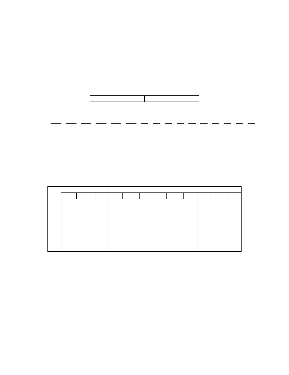
MOTOROLA INSTRUCTION SET DETAILS M68HC11
A-92 REFERENCE MANUAL
STD Store Double Accumulator STD
Operation: M : M + 1 ⇐(ACCD); M ⇐(ACCA), M + 1 ⇐(ACCB)
Description: Stores the contents of double accumulator ACCD in memory. The contents
of ACCD remain unchanged.
Condition Codes and Boolean Formulae:
N D15
Set if MSB of result is set; cleared otherwise.
ZD15 • D14 • D13 • D12 • D11 • D10 • D9 • D8 • D7 • D6 • D5 • D4 • D3 • D2 • D1 • D0
Set if result is $0000; cleared otherwise.
V0
Cleared
Source Forms: STD (opr)
Addressing Modes, Machine Code, and Cycle-by-Cycle Execution:
SXHINZVC
———— ∆∆0—
Cycle STD (DIR) STD (EXT) STD (IND,X) STD (IND,Y)
Addr Data R/W Addr Data R/W Addr Data R/W Addr Data R/W
1 OP DD 1 OP FD 1 OP ED 1 OP 18 1
2 OP+1 dd 1 OP+1 hh 1 OP+1 ff 1 OP+1 ED 1
3 00dd (A) 1 OP+2 ll 1 FFFF — 1 OP+2 ff 1
400dd+
1(B) 1 hhll (A) 1 X+ff (A) 1 FFFF — 1
5 hhll+1 (B) 1 X+ff+
1(B) 1 Y+ff (A) 1
6Y+ff+
1(B) 1

M68HC11 INSTRUCTION SET DETAILS MOTOROLA
REFERENCE MANUAL A-93
STOP Stop Processing STOP
Description: If the S bit in the CCR is set, then the STOP instruction is disabled and op-
erates like the NOP instruction. If the S bit in the CCR is clear, the STOP instruction
causes all system clocks to halt, and the system is placed in a minimum-power
standby mode. All CPU registers remain unchanged. I/O pins also remain unaffect-
ed.
Recovery from STOP may be accomplished by RESET, XIRQ, or an unmasked
IRQ. When recovering from STOP with XIRQ, if the X bit in the CCR is clear, exe-
cution will resume with the stacking operations for the XIRQ interrupt. If the X bit in
the CCR is set, masking XIRQ interrupts, execution will resume with the opcode
fetch for the instruction which follows the STOP instruction (continue).
An error in some mask sets of the M68HC11 caused incorrect recover from STOP
under very specific unusual conditions. If the opcode of the instruction before the
STOP instruction came from column 4 or 5 of the opcode map, the STOP instruc-
tion was incorrectly interpreted as a two-byte instruction. A simple way to avoid this
potential problem is to put a NOP instruction (which is a column 0 opcode) imme-
diately before any STOP instruction.
Condition Codes and Boolean Formulae:
None affected
Source Forms: STOP
Addressing Modes, Machine Code, and Cycle-by-Cycle Execution:
SXHINZVC
————————
Cycle STOP (INH)
Addr Data R/W
1OPCF1
2 OP+1 — 1
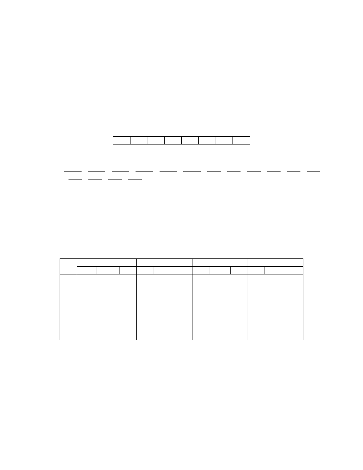
MOTOROLA INSTRUCTION SET DETAILS M68HC11
A-94 REFERENCE MANUAL
STS Store Stack Pointer ST
Operation: M ⇐(SPH), M + 1 ⇐(SPL)
Description: Stores the most significant byte of the stack pointer in memory at the ad-
dress specified by the program and stores the least significant byte of the stack
pointer at the next location in memory, at one plus the address specified by the pro-
gram.
Condition Codes and Boolean Formulae:
N SP15
Set if MSB of result is set; cleared otherwise.
ZSP15 • SP14 • SP13 • SP12 • SP11 • SP10 • SP9 • SP8 • SP7 • SP6 • SP5 • SP4
•SP3 • SP2 • SP1 • SP0
Set if result is $0000; cleared otherwise.
V0
Cleared
Source Forms: STS (opr)
Addressing Modes, Machine Code, and Cycle-by-Cycle Execution:
SXHINZVC
———— ∆∆0—
Cycle STS (DIR) STS (EXT) STS (IND,X) STS (IND,Y)
Addr Data R/W Addr Data R/W Addr Data R/W Addr Data R/W
1 OP 9F 1 OP BF 1 OP AF 1 OP 18 1
2 OP+1 dd 1 OP+1 hh 1 OP+1 ff 1 OP+1 AF 1
3 00dd (SPH) 0 OP+2 ll 1 FFFF — 1 OP+2 ff 1
400dd+
1(SPL) 0 hhll (SPH) 0 X+ff (SPH) 0 FFFF — 1
5 hhll+1 (SPL) 0 X+ff+
1(SPL) 0 Y+ff (SPH) 0
6Y+ff+
1(SPL) 0
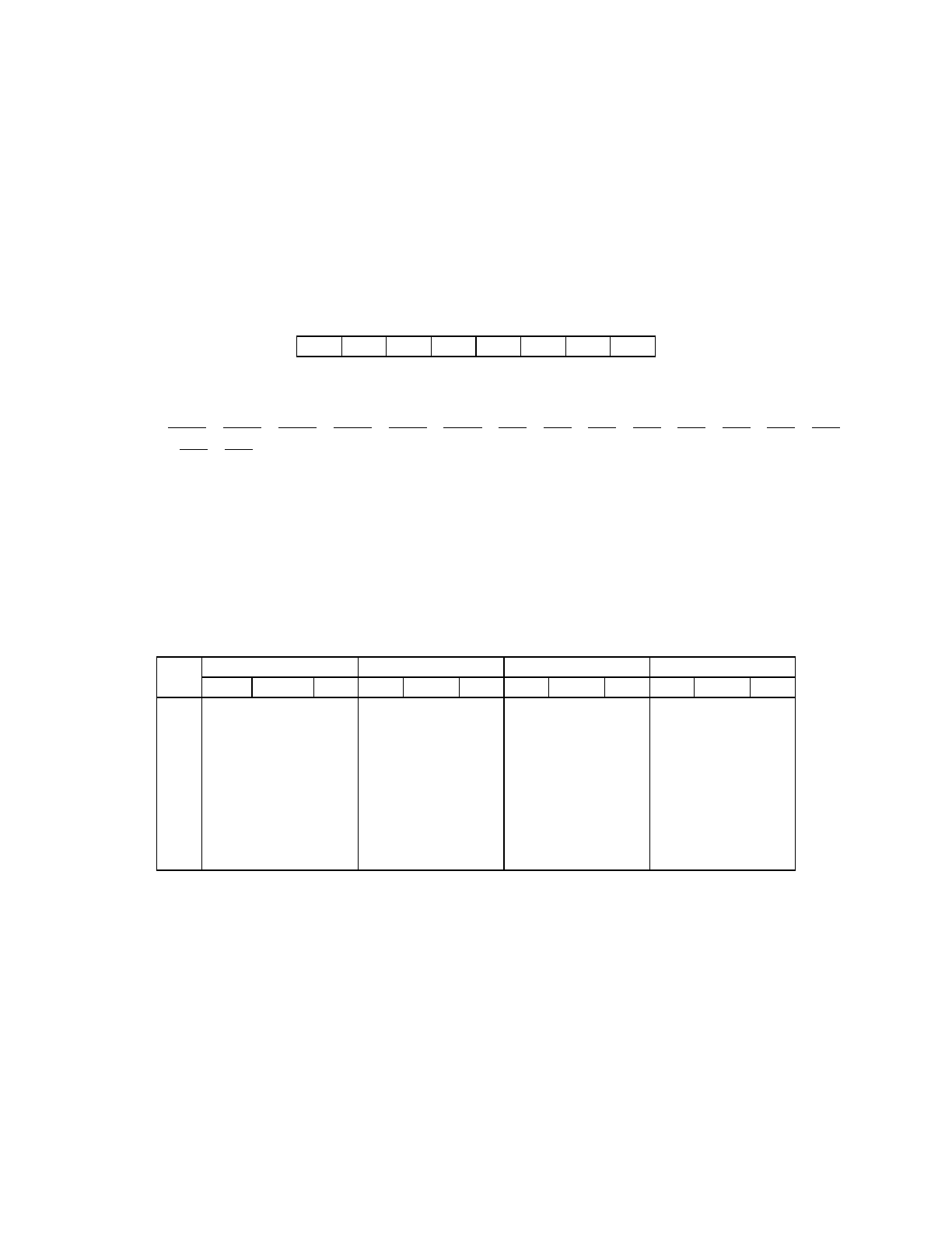
M68HC11 INSTRUCTION SET DETAILS MOTOROLA
REFERENCE MANUAL A-95
STX Store Index Register X STX
Operation: M ⇐(IXH), M + 1 ⇐(IXL)
Description: Stores the most significant byte of index register X in memory at the address
specified by the program, and stores the least significant byte of index register X
at the next location in memory, at one plus the address specified by the program.
Condition Codes and Boolean Formulae:
N IX15
Set if MSB of result is set; cleared otherwise.
ZIX15 • IX14 • IX13 • IX12 • IX11 • IX10 • IX9 • IX8 • IX7 • IX6 • IX5 • IX4 • IX3 • IX2
•IX1 • IX0
Set if result is $0000; cleared otherwise.
V0
Cleared
Source Forms: STX (opr)
Addressing Modes, Machine Code, and Cycle-by-Cycle Execution:
SXHINZVC
———— ∆∆0—
Cycle STX (DIR) STX (EXT) STX (IND,X) STX (IND,Y)
Addr Data R/W Addr Data R/W Addr Data R/W Addr Data R/W
1 OP DF 1 OP FF 1 OP EF 1 OP CD 1
2 OP+1 dd 1 OP+1 hh 1 OP+1 ff 1 OP+1 EF 1
3 00dd (IXH) 0 OP+2 ll 1 FFFF — 1 OP+2 ff 1
400dd+
1(IXL) 0 hhll (IXH) 0 X+ff (IXH) 0 FFFF — 1
5 hhll+1 (IXL) 0 X+ff+
1(IXL) 0 Y+ff (IXH) 0
6Y+ff+
1(IXL) 0

MOTOROLA INSTRUCTION SET DETAILS M68HC11
A-96 REFERENCE MANUAL
STY Store Index Register Y STY
Operation: M ⇐(IYH), M + 1 ⇐(IYL)
Description: Stores the most significant byte of index register Y in memory at the address
specified by the program, and stores the least significant byte of index register Y
at the next location in memory, at one plus the address specified by the program.
Condition Codes and Boolean Formulae:
N IY15
Set if MSB of result is set; cleared otherwise.
ZIY15 • IY14 • IY13 • IY12 • IY11 • IY10 • IY9 • IY8 • IY7 • IY6 • IY5 • IY4 • IY3 • IY2
•IY1 • IY0
Set if result is $0000; cleared otherwise.
V0
Cleared
Source Forms: STY (opr)
Addressing Modes, Machine Code, and Cycle-by-Cycle Execution:
SXHINZVC
———— ∆∆0—
Cycle STY (DIR) STY (EXT) STY (IND,X) STY (IND,Y)
Addr Data R/W Addr Data R/W Addr Data R/W Addr Data R/W
1 OP DF 1 OP FF 1 OP EF 1 OP CD 1
2 OP+1 dd 1 OP+1 hh 1 OP+1 ff 1 OP+1 EF 1
3 00dd (IYH) 0 OP+2 ll 1 FFFF — 1 OP+2 ff 1
400dd+
1(IYL) 0 hhll (IYH) 0 X+ff (IYH) 0 FFFF — 1
5 hhll+1 (IYL) 0 X+ff+
1(IYL) 0 Y+ff (IYH) 0
6Y+ff+
1(IYL) 0
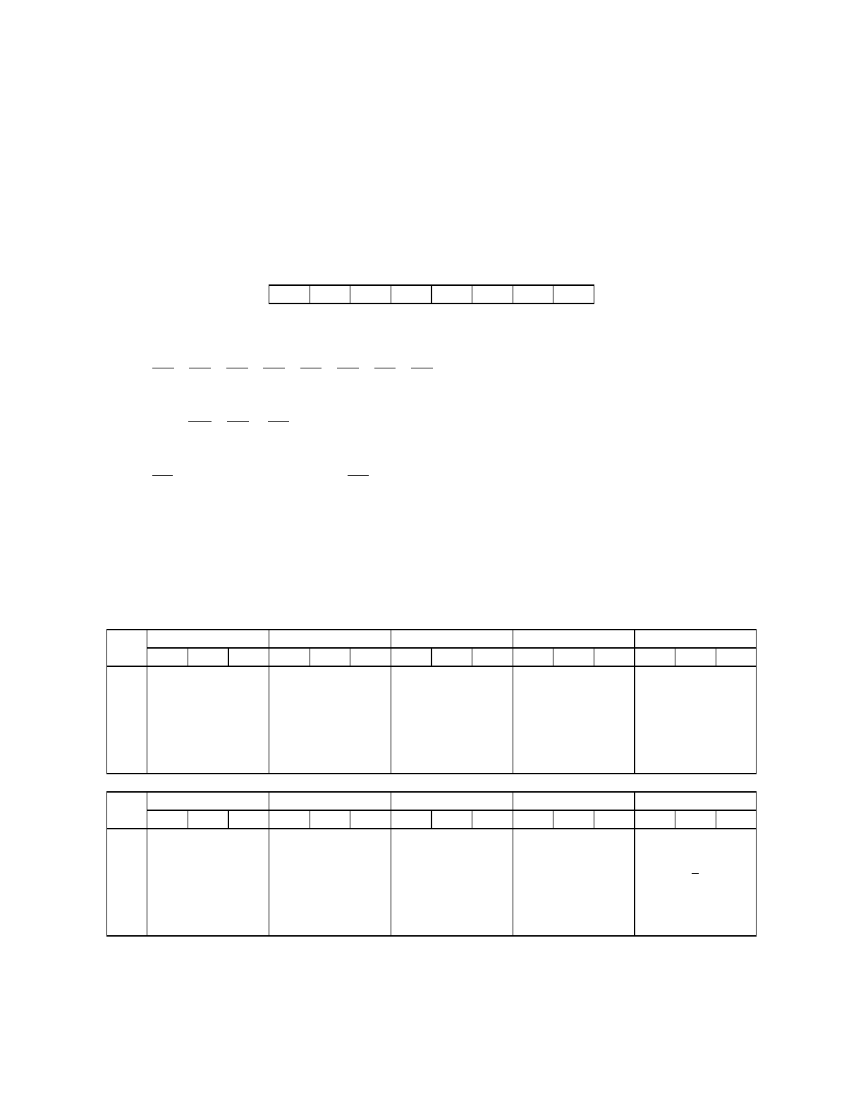
M68HC11 INSTRUCTION SET DETAILS MOTOROLA
REFERENCE MANUAL A-97
SUB Subtract SUB
Operation: ACCX ⇐(ACCX) – (M)
Description: Subtracts the contents of M from the contents of ACCX and places the result
in ACCX. For subtract instructions, the C bit in the CCR represents a borrow.
Condition Codes and Boolean Formulae:
NR7
Set if MSB of result is set; cleared otherwise.
ZR7 • R6 • R5 • R4 • R3 • R2 • R1 • R0
Set if result is $00; cleared otherwise.
V X7 • M7 • R7 + X7 • M7 • R7
Set if a two’s complement overflow resulted from the operation; cleared otherwise.
CX7 • M7 + M7 • R7 + R7 • X7
Set if the absolute value of the contents of memory plus previous carry is larger
than the absolute value of the accumulator; cleared otherwise.
Source Forms: SUBA (opr); SUBB (opr)
Addressing Modes, Machine Code, and Cycle-by-Cycle Execution:
SXHINZVC
———— ∆∆∆∆
Cycle SUBA (IMM) SUBA (DIR) SUBA (EXT) SUBA (IND,X) SUBA (IND,Y)
Addr Data R/W Addr Data R/W Addr Data R/W Addr Data R/W Addr Data R/W
1 OP 80 1 OP 90 1 OP B0 1 OP A0 1 OP 18 1
2 OP+1 ii 1 OP+1 dd 1 OP+1 hh 1 OP+1 ff 1 OP+1 A0 1
3 00dd (00dd
)1 OP+2 ll 1 FFFF — 1 OP+2 ff 1
4 hhll (hhll) 1 X+ff (X+ff) 1 FFFF — 1
5 Y+ff (Y+ff) 1
Cycle SUBB (IMM) SUBB (DIR) SUBB (EXT) SUBB (IND,X) SUBB (IND,Y)
Addr Data R/W Addr Data R/W Addr Data R/W Addr Data R/W Addr Data R/W
1 OP C0 1 OP D0 1 OP F0 1 OP E0 1 OP 18 1
2 OP+1 ii 1 OP+1 dd 1 OP+1 hh 1 OP+1 ff 1 OP+1 E0 1
3 00dd (00dd
)1 OP+2 ll 1 FFFF — 1 OP+2 ff 1
4 hhll (hhll) 1 X+ff (X+ff) 1 FFFF — 1
5 Y+ff (Y+ff) 1
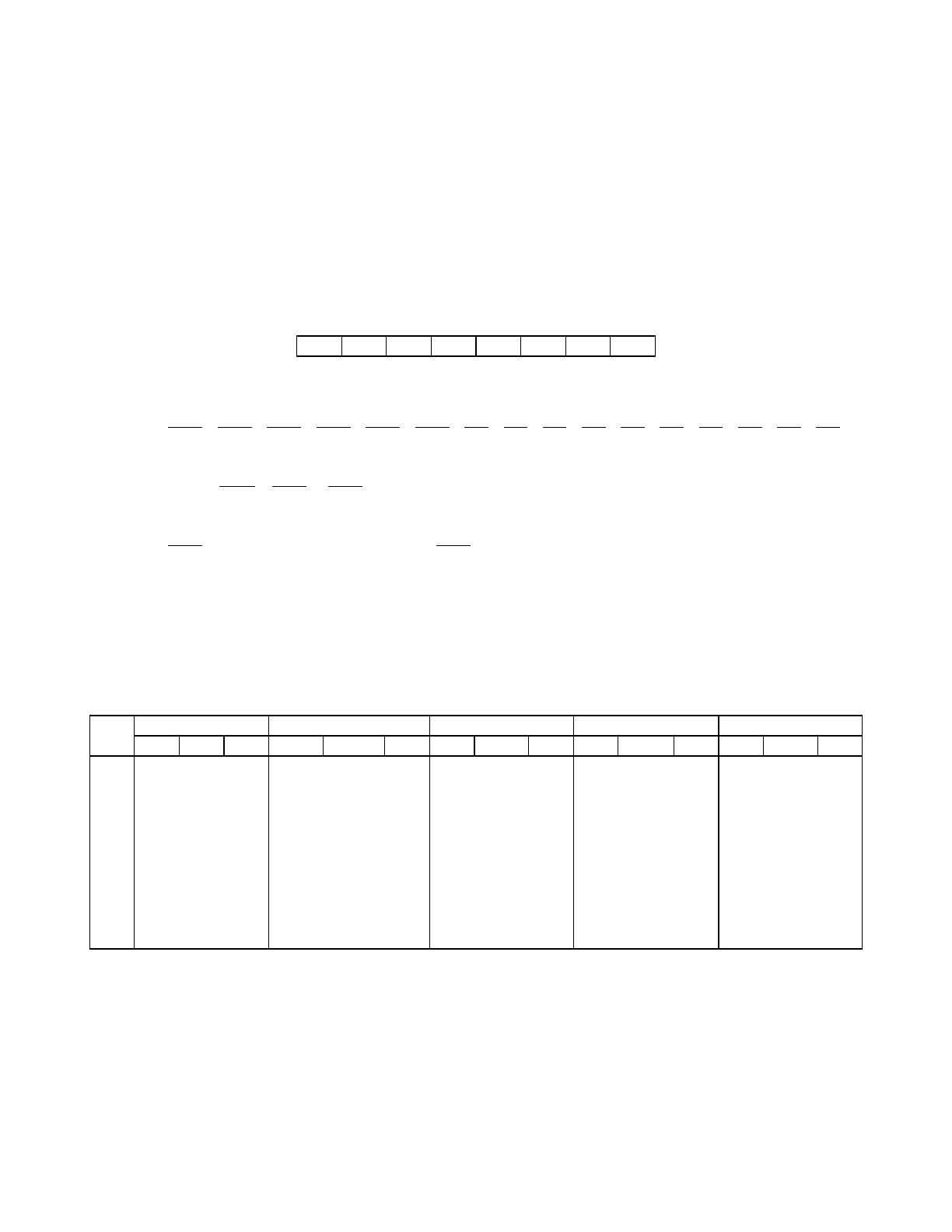
MOTOROLA INSTRUCTION SET DETAILS M68HC11
A-98 REFERENCE MANUAL
SUBD Subtract Double Accumulator SUBD
Operation: ACCD ⇐(ACCD) – (M : M + 1)
Description: Subtracts the contents ofM:M+1from the contents of double accumulator
D and places the result in ACCD. For subtract instructions, the C bit in the CCR
represents a borrow.
Condition Codes and Boolean Formulae:
N R15
Set if MSB of result is set; cleared otherwise.
ZR15 • R14 • R13 • R12 • R11 • R10 • R9 • R8 • R7 • R6 • R5 • R4 • R3 • R2 • R1 • R0
Set if result is $0000; cleared otherwise.
V D15 • M15 • R15 + D15 • M15 • R15
Set if a two’s complement overflow resulted from the operation; cleared otherwise.
CD15 • M15 + M15 • R15 + R15 • D15
Set if the absolute value of the contents of memory is larger than the absolute value
of the accumulator; cleared otherwise.
Source Forms: SUBD (opr)
Addressing Modes, Machine Code, and Cycle-by-Cycle Execution:
SXHINZVC
———— ∆∆∆∆
Cycle SUBD (IMM) SUBD (DIR) SUBD (EXT) SUBD (IND,X) SUBD (IND,Y)
Addr Data R/W Addr Data R/W Addr Data R/W Addr Data R/W Addr Data R/W
1 OP 83 1 OP 93 1 OP B3 1 OP A3 1 OP 18 1
2 OP+1 jj 1 OP+1 dd 1 OP+1 hh 1 OP+1 ff 1 OP+1 A3 1
3 OP+2 kk 1 00dd (00dd) 1 OP+2 hh 1 FFFF — 1 OP+2 ff 1
4 FFFF — 1 00dd+1 (00dd+1
)1 hhll (hhll) 1 X+ff (X+ff) 1 FFFF — 1
5 FFFF — 1 hhll+1 (hhll+1) 1 X+ff+
1(X+ff+1
)1 Y+ff (Y+ff) 1
6 FFFF — 1 FFFF — 1 Y+ff+
1(Y+ff+1
)1
7 FFFF — 1

M68HC11 INSTRUCTION SET DETAILS MOTOROLA
REFERENCE MANUAL A-99
SWI Software Interrupt SWI
Operation: PC⇐(PC)+ $0001
⇓ (PCL), SP⇐(SP) – $0001
⇓ (PCH), SP⇐(SP) – $0001
⇓ (IYL), SP⇐(SP) – $0001
⇓ (IYH), SP⇐(SP) – $0001
⇓ (IXL), SP⇐(SP) – $0001
⇓ (IXH), SP⇐(SP) – $0001
⇓ (ACCA), SP⇐(SP) – $0001
⇓ (ACCB), SP⇐(SP) – $0001
⇓ (CCR), SP⇐(SP) – $0001
I⇐ 1, PC ⇐ (SWI vector)
Description: The program counter is incremented by one. The program counter, index
registers Y and X, and accumulators A and B are pushed onto the stack. The CCR
is then pushed onto the stack. The stack pointer is decremented by one after each
byte of data is stored on the stack. The I bit in the CCR is then set. The program
counter is loaded with the address stored at the SWI vector, and instruction execu-
tion resumes at this location. This instruction is not maskable by the I bit.
Condition Codes and Boolean Formulae:
I1
Set
Source Forms: SWI
Addressing Modes, Machine Code, and Cycle-by-Cycle Execution:
SXHINZVC
——— 1 ————
Cycle SWI (INH)
Addr Data R/W
1OP3F 1
2 OP+1 — 1
3 SP Rtn lo 0
4 SP–1 Rtn hi 0
5 SP–2 (IYL) 0
6 SP–3 (IYH) 0
7 SP–4 (IXL) 0
8 SP–5 (IXH) 0
9 SP–6 (A) 0
10 SP–7 (B) 0
11 SP–8 (CCR) 0
12 SP–8 (CCR) 1
13 Vec hi Svc hi 1
14 Vec lo Svc lo 1

MOTOROLA INSTRUCTION SET DETAILS M68HC11
A-100 REFERENCE MANUAL
TAB Transfer from Accumulator A to B TAB
Operation: ACCB ⇐(ACCA)
Description: Moves the contents of ACCA to ACCB. The former contents of ACCB are
lost; the contents of ACCA are not affected.
Condition Codes and Boolean Formulae:
NR7
Set if MSB of result is set; cleared otherwise.
ZR7 • R6 • R5 • R4 • R3 • R2 • R1 • R0
Set if result is $00; cleared otherwise.
V0
Cleared.
Source Forms: TAB
Addressing Modes, Machine Code, and Cycle-by-Cycle Execution:
SXHINZVC
———— ∆∆0—
Cycle TAB (INH)
Addr Data R/W
1OP16 1
2 OP+1 — 1
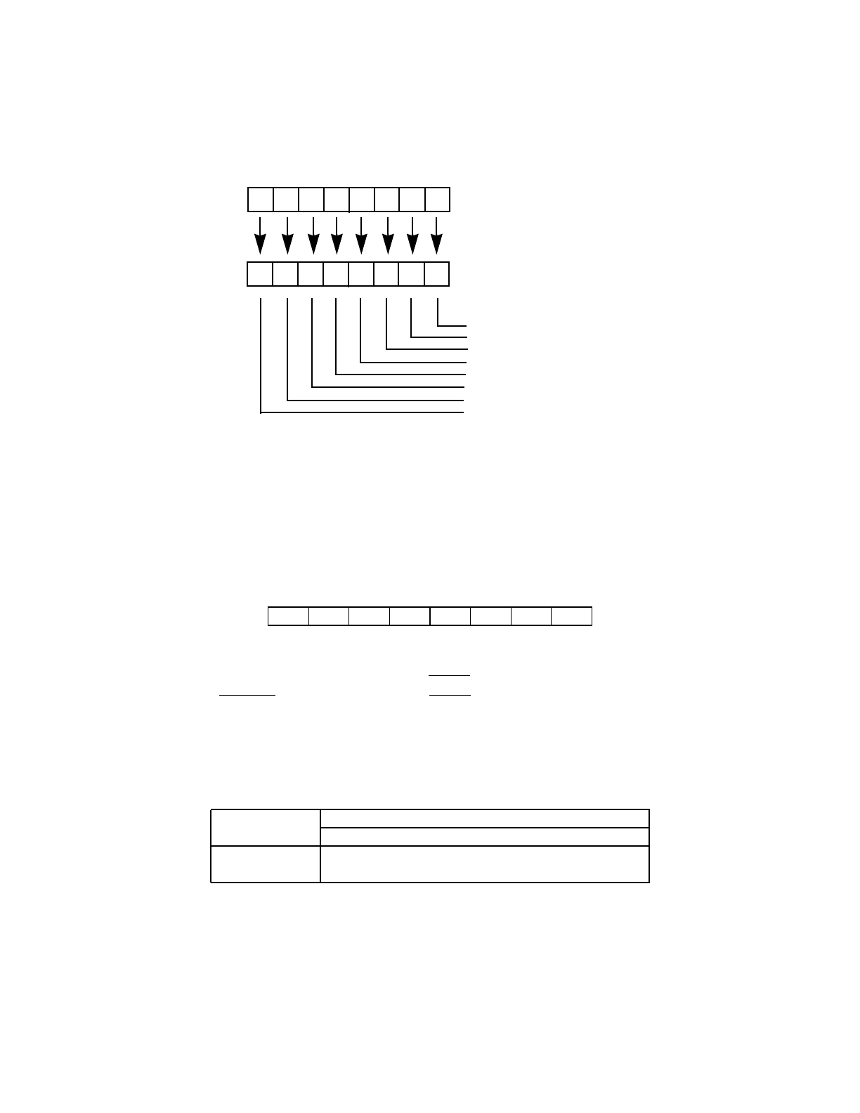
M68HC11 INSTRUCTION SET DETAILS MOTOROLA
REFERENCE MANUAL A-101
TAP Transfer from Accumulator A to CCR TAP
Operation: CCR ⇐(ACCA)
Description: Transfers the contents of bit positions 7–0 of accumulator A to the corre-
sponding bit positions of the CCR. The contents of accumulator A remain un-
changed. The X bit in the CCR may be cleared as a result of a TAP instruction but
may not be set if it was clear prior to execution of the TAP instruction.
Condition Codes and Boolean Formulae:
Condition code bits take on the value of the corresponding bit of accumulator A except
that the X bit may not change from a zero to a one. Software can leave X set, leave X
clear, or change X from one to zero. The XIRQ interrupt mask can only become set as
a result of a RESET or recognition of an XIRQ interrupt.
Source Forms: TAP
Addressing Modes, Machine Code, and Cycle-by-Cycle Execution:
SXHINZVC
∆⇓∆∆∆∆∆∆
Cycle TAP (INH)
Addr Data R/W
1OP06 1
2 OP+1 — 1
76 5432 1 0
ACCA
CCR
Carry/Borrow
Overflow (Two’s Complement)
Zero
Negative
I Interrupt Mask
Half Carry
X Interrupt Mask
Stop Disable
Bit Positions
SXHI NZVC
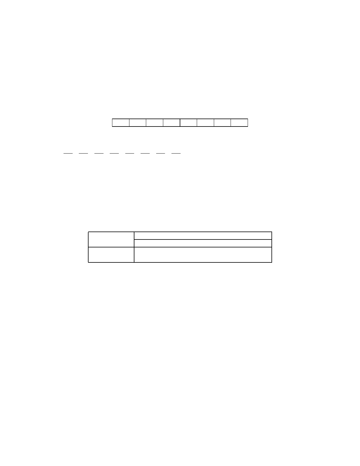
MOTOROLA INSTRUCTION SET DETAILS M68HC11
A-102 REFERENCE MANUAL
TBA Transfer from Accumulator B to A TBA
Operation: ACCA ⇐(ACCB)
Description: Moves the contents of ACCB to ACCA. The former contents of ACCA are
lost; the contents of ACCB are not affected.
Condition Codes and Boolean Formulae:
NR7
Set if MSB of result is set; cleared otherwise.
ZR7 • R6 • R5 • R4 • R3 • R2 • R1 • R0
Set if result is $00; cleared otherwise.
V0
Cleared.
Source Forms: TBA
Addressing Modes, Machine Code, and Cycle-by-Cycle Execution:
SXHINZVC
———— ∆∆0—
Cycle TBA (INH)
Addr Data R/W
1OP17 1
2 OP+1 — 1

M68HC11 INSTRUCTION SET DETAILS MOTOROLA
REFERENCE MANUAL A-103
TEST Test Operation (Test Mode Only) TEST
Description: This is a single-byte instruction that causes the program counter to be con-
tinuously incremented. It can only be executed while in the test mode. The MPU
must be reset to exit this instruction. Code execution is suspended during this in-
struction. This is an illegal opcode when not in test mode.
Condition Codes and Boolean Formulae:
None affected
Source Forms: TEST
Addressing Modes, Machine Code, and Cycle-by-Cycle Execution:
SXHINZVC
————————
Cycle TEST (INH)
Addr Data R/W
1OP00 1
2 OP+1 — 1
3 OP+2 — 1
4 OP+3 — 1
5–n PREV–1 (PREV–1) 1
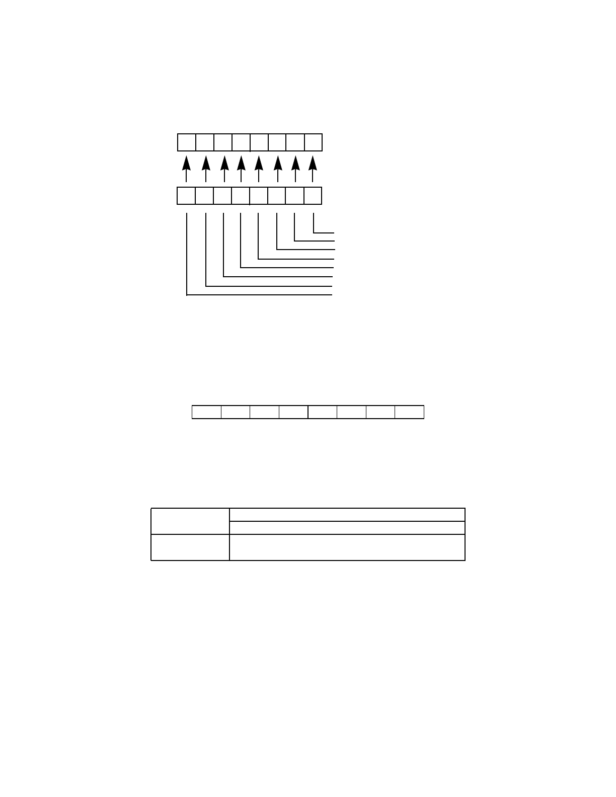
MOTOROLA INSTRUCTION SET DETAILS M68HC11
A-104 REFERENCE MANUAL
TPA Transfer from CCR to Accumulator A TPA
Operation: (ACCA) ⇐(CCR)
Description: Transfers the contents of the CCR to corresponding bit positions of accu-
mulator A. The CCR remains unchanged.
Condition Codes and Boolean Formulae:
None affected
Source Forms: TPA
Addressing Modes, Machine Code, and Cycle-by-Cycle Execution:
SXHINZVC
————————
Cycle TPA (INH)
Addr Data R/W
1OP07 1
2 OP+1 — 1
76 5432 1 0
ACCA
CCR
Carry/Borrow
Overflow (Two’s Complement)
Zero
Negative
I Interrupt Mask
Half Carry
X Interrupt Mask
Stop Disable
Bit Positions
SXHI NZVC
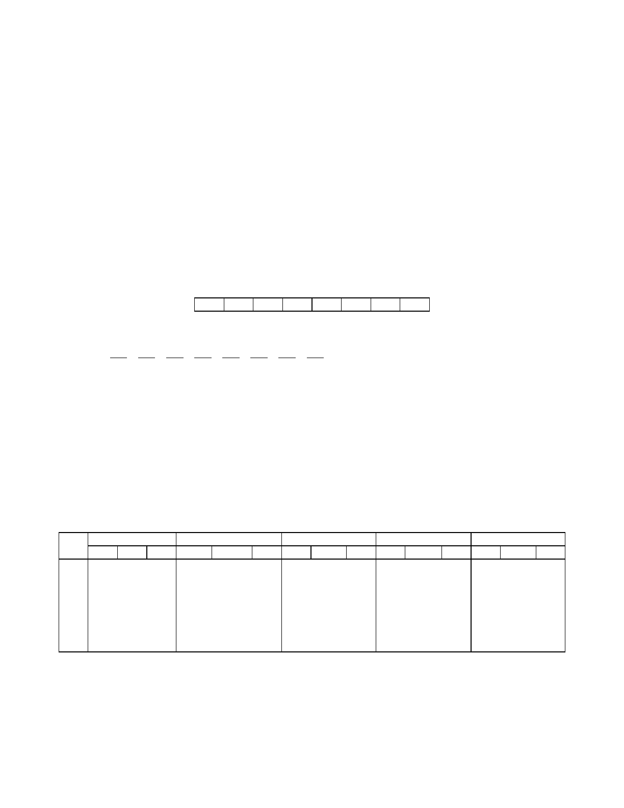
M68HC11 INSTRUCTION SET DETAILS MOTOROLA
REFERENCE MANUAL A-105
TST Test TST
Operation: (ACCX) – $00 or: (M) – $00
Description: Subtracts $00 from the contents of ACCX or M and sets the condition codes
accordingly.
The subtraction is accomplished internally without modifying either ACCX or M.
The TST instruction provides only minimum information when testing unsigned val-
ues. Since no unsigned value is less than zero, BLO and BLX have no utility. While
BHI could be used after TST, it provides exactly the same control as BNE, which
is preferred. After testing signed values, all signed branches are available.
Condition Codes and Boolean Formulae:
NR7
Set if MSB of result is set; cleared otherwise.
ZM7 • M6 • M5 • M4 • M3 • M2 • M1 • M0
Set if result is $00; cleared otherwise.
V0
Cleared
C0
Cleared
Source Forms: TSTA; TSTB; TST (opr)
Addressing Modes, Machine Code, and Cycle-by-Cycle Execution:
SXHINZVC
———— ∆∆00
Cycle TSTA (INH) TSTB (INH) TST (EXT) TST (IND,X) TST (IND,Y)
Addr Data R/W Addr Data R/W Addr Data R/W Addr Data R/W Addr Data R/W
1 OP 4D 1 OP 5D 1 OP 7D 1 OP 6D 1 OP 18 1
2 OP+1 — 1 OP+1 — 1 OP+1 hh 1 OP+1 ff 1 OP+1 6D 1
3 OP+2 ll 1 FFFF — 1 OP+2 ff 1
4 hhll (hhll) 1 X+ff (X+ff) 1 FFFF — 1
5 FFFF — 1 FFFF — 1 Y+ff (Y+ff) 1
6 FFFF — 1 FFFF — 1 FFFF — 1
7 FFFF — 1

MOTOROLA INSTRUCTION SET DETAILS M68HC11
A-106 REFERENCE MANUAL
TSX Transfer from SP to Index Register X TSX
Operation: IX ⇐(SP) + $0001
Description: Loads the index register X with one plus the contents of the stack pointer.
The contents of the stack pointer remain unchanged. After a TSX instruction the
index register X points at the last value that was stored on the stack.
Condition Codes and Boolean Formulae:
None affected
Source Forms: TSX
Addressing Modes, Machine Code, and Cycle-by-Cycle Execution:
SXHINZVC
————————
Cycle TSX (INH)
Addr Data R/W
1OP30 1
2 OP+1 — 1
3SP— 1

M68HC11 INSTRUCTION SET DETAILS MOTOROLA
REFERENCE MANUAL A-107
TSY Transfer from SP to Index Register Y TSY
Operation: IY ⇐(SP) + $0001
Description: Loads the index register Y with one plus the contents of the stack pointer.
The contents of the stack pointer remain unchanged. After a TSY instruction the
index register Y points at the last value that was stored on the stack.
Condition Codes and Boolean Formulae:
None affected
Source Forms: TSY
Addressing Modes, Machine Code, and Cycle-by-Cycle Execution:
SXHINZVC
————————
Cycle TSY (INH)
Addr Data R/W
1OP18 1
2 OP+1 30 1
3 OP+2 — 1
4SP— 1

MOTOROLA INSTRUCTION SET DETAILS M68HC11
A-108 REFERENCE MANUAL
TXS Transfer from Index Register X to SP TXS
Operation: SP ⇐(IX) – $0001
Description: Loads the stack pointer with the contents of index register X minus one. The
contents of index register X remain unchanged.
Condition Codes and Boolean Formulae:
None affected
Source Forms: TXS
Addressing Modes, Machine Code, and Cycle-by-Cycle Execution:
SXHINZVC
————————
Cycle TXS (INH)
Addr Data R/W
1OP35 1
2 OP+1 — 1
3 FFFF — 1

M68HC11 INSTRUCTION SET DETAILS MOTOROLA
REFERENCE MANUAL A-109
TYS Transfer from Index Register Y to SP TYS
Operation: SP ⇐(IY) – $0001
Description: Loads the stack pointer with the contents of index register Y minus one. The
contents of index register Y remain unchanged.
Condition Codes and Boolean Formulae:
None affected
Source Forms: TYS
Addressing Modes, Machine Code, and Cycle-by-Cycle Execution:
SXHINZVC
————————
Cycle TYS (INH)
Addr Data R/W
1OP18 1
2 OP+1 35 1
3 OP+2 — 1
4 FFFF — 1

MOTOROLA INSTRUCTION SET DETAILS M68HC11
A-110 REFERENCE MANUAL
WAI Wait for Interrupt WAI
Operation: PC⇐(PC)+ $0001
⇓ (PCL), SP⇐(SP) – $0001
⇓ (PCH), SP⇐(SP) – $0001
⇓ (IYL), SP⇐(SP) – $0001
⇓ (IYH), SP⇐(SP) – $0001
⇓ (IXL), SP⇐(SP) – $0001
⇓ (IXH), SP⇐(SP) – $0001
⇓ (ACCA), SP⇐(SP) – $0001
⇓ (ACCB), SP⇐(SP) – $0001
⇓ (CCR), SP⇐(SP) – $0001
Description: The program counter is incremented by one. The program counter, index
registers Y and X, and accumulators A and B are pushed onto the stack. The CCR
is then pushed onto the stack. The stack pointer is decremented by one after each
byte of data is stored on the stack.
The MPU then enters a wait state for an integer number of MPU E-clock cycles.
While in the wait state, the address/data bus repeatedly runs read bus cycles to the
address where the CCR contents were stacked. The MPU leaves the wait state
when it senses any interrupt that has not been masked.
Upon leaving the wait state, the MPU sets the I bit in the CCR, fetches the vector
(address) corresponding to the interrupt sensed, and instruction execution is re-
sumed at this location.
Condition Codes and Boolean Formulae:
Although the WAI instruction itself does not alter the condition code bits, the inter-
rupt which causes the MCU to resume processing causes the I bit (and the X bit if
the interrupt was XIRQ) to be set as the interrupt vector is being fetched.
SXHINZVC
——— 1 ————

M68HC11 INSTRUCTION SET DETAILS MOTOROLA
REFERENCE MANUAL A-111
WAI Wait for Interrupt (Continued) WAI
Source Forms: WAI
Addressing Modes, Machine Code, and Cycle-by-Cycle Execution:
Cycle WAI (INH)
Addr Data R/W
1OP3E1
2 OP+1 — 1
3 SP Rtn lo 0
4 SP–1 Rtn hi 0
5 SP–2 (IYL) 0
6 SP–3 (IYH) 0
7 SP–4 (IXL) 0
8 SP–5 (IXH) 0
9 SP–6 (A) 0
10 SP–7 (B) 0
11 SP–8 (CCR) 0
12 SP–8 (CCR) 1
13 Vec hi Svc hi 1
14 Vec lo Svc lo 1

MOTOROLA INSTRUCTION SET DETAILS M68HC11
A-112 REFERENCE MANUAL
XGDX Exchange Double Accumulator and XGDX
Index Register X
Operation: (IX) ⇐⇒ (ACCD)
Description: Exchanges the contents of double accumulator ACCD and the contents of
index register X. A common use for XGDX is to move an index value into the dou-
ble accumulator to allow 16-bit arithmetic calculations on the index value before ex-
changed the updated index value back into the X index register.
Condition Codes and Boolean Formulae:
None affected
Source Forms: XGDX
Addressing Modes, Machine Code, and Cycle-by-Cycle Execution:
SXHINZVC
————————
Cycle XGDX (INH)
Addr Data R/W
1OP8F 1
2 OP+1 — 1
3 FFFF — 1

M68HC11 INSTRUCTION SET DETAILS MOTOROLA
REFERENCE MANUAL A-113
XGDY Exchange Double Accumulator and XGDY
Index Register Y
Operation: (IY) ⇐⇒ (ACCD)
Description: Exchanges the contents of double accumulator ACCD and the contents of
index register Y. A common use for XGDY is to move an index value into the dou-
ble accumulator to allow 16-bit arithmetic calculations on the index value before ex-
changed the updated index value back into the Y index register.
Condition Codes and Boolean Formulae:
None affected
Source Forms: XGDY
Addressing Modes, Machine Code, and Cycle-by-Cycle Execution:
SXHINZVC
————————
Cycle XGDY (INH)
Addr Data R/W
1OP18 1
2 OP+1 8F 1
3 OP+2 — 1
4 FFFF — 1

MOTOROLA INSTRUCTION SET DETAILS M68HC11
A-114 REFERENCE MANUAL

M68HC11 BOOTLOADER LISTINGS MOTOROLA
REFERENCE MANUAL B-1
APPENDIX B
BOOTLOADER LISTINGS
This appendix contains source code listings of the internal bootloader ROMs for sev-
eral members of the M68HC11 Family.
Listings of other M68HC11 Family bootloader ROMs can be found in application note
AN1060.
Family Security Option Page
MC68HC11A8 No B–2 to B–4
MC68HC11A8 Yes B–5 to B–8
MC68HC811E2 No B–9 to B–11
MC68HC811E2 Yes B–12 to B–16
MC68HC11E9 No B–17 to B–19
MC68HC11E9 Yes B–20 to B–24
MC68HC11F1 No B–25 to B–27

MOTOROLA BOOTLOADER LISTINGS M68HC11
B-2 REFERENCE MANUAL
Listing MC68HC11A8 Bootloader (No Security) Sheet 1 of 3
* BOOTLOADER FIRMWARE FOR MC68HC11A8 W/O SECURITY
***************************************************
* Thu Dec 11 18:46:19 CST 1986
***************************************************
* EQUATES FOR USE WITH INDEX OFFSET = $1000
0008 PORTD EQU $08
0009 DDRD EQU $09
0028 SPCR EQU $28 (FOR DWOM BIT)
002b BAUD EQU $2B
002c SCCR1 EQU $2C
002d SCCR2 EQU $2D
002e SCSR EQU $2E
002f SCDAT EQU $2F
003b PPROG EQU $3B
003e TEST1 EQU $3E
003f CONFIG EQU $3F
* MORE EQUATES
*
b600 EEPSTR EQU $B600 START OF EEPROM
b7ff EEPEND EQU $B7FF END OF EEPROM
*****************************************************
* THIS BOOTSTRAP PROGRAM ALLOWS THE USER TO
* DOWNLOAD A PROGRAM OF EXACTLY 256 BYTES.
* THE PROGRAM MUST START AT $0000.
* EACH BYTE OF THE PROGRAM IS RECEIVED BY THE
* SCI, STARTING WITH THE $0000 BYTE AND WORKING
* UP TO THE $00FF BYTE.
*
* THE TRANSMITTER WILL BE USED FOR THE PURPOSE
* OF COMMUNICATION TO THE OUTSIDE WORLD.
*****************************************************
bf40 ORG $BF40
bf40 BEGIN EQU *
* INIT STACK
bf40 8e 00 ff LDS #$00FF
* INIT X REG FOR INDEXED ACCESS TO REGISTERS
bf43 ce 10 00 LDX #$1000
* PUT PORT D IN WIRE OR MODE
bf46 1c 28 20 BSET SPCR,X $20
* INIT SCI AND RESTART BAUD DIVIDER CHAIN
bf49 86 a2 LDAA #$A2 DIV BY 16
bf4b a7 2b STAA BAUD,X
* RECEIVER & TRANSMITTER ENABLED
bf4d 86 0c LDAA #$0C
bf4f a7 2d STAA SCCR2,X

M68HC11 BOOTLOADER LISTINGS MOTOROLA
REFERENCE MANUAL B-3
Listing - MC68HC11A8 Bootloader (No Security) Sheet 2 of 3
* SECURITY CODE IS REMOVED
* SEND BREAK TO SIGNAL START OF DOWNLOAD
bf51 1c 2d 01 BSET SCCR2,X $01
* CLEAR BREAK AS SOON AS START BIT IS DETECTED
bf54 1e 08 01 fc BRSET PORTD,X $01 *
bf58 1d 2d 01 BCLR SCCR2,X $01 CLEAR BREAK
* WAIT FOR FIRST CHARACTER (USERS SEND $FF)
bf5b 1f 2e 20 fc BRCLR SCSR,X $20 * WAIT FOR RDRF
bf5f a6 2f LDAA SCDAT,X READ DATA
* IF DATA = $00 (BREAK OR $00), THEN JUMP TO EEPROM
bf61 26 03 BNE NOTZERO
bf63 7e b6 00 JMP $B600
bf66 NOTZERO EQU *
* IF DATA = $55, THEN SKIP DOWNLOAD (TEST MODE)
bf66 81 55 CMPA #$55
bf68 27 1e BEQ STAR
* IF DATA = $FF, THEN /16 IS CORRECT BAUD
bf6a 81 ff CMPA #$FF
bf6c 27 03 BEQ BAUDOK
* ELSE CHANGE TO /104 (/13 & /8) 1200 @ 2MHZ
bf6e 1c 2b 33 BSET BAUD,X $33
* THEN DOWNLOAD 256 BYTE PROGRAM
bf71 BAUDOK EQU *
bf71 18 ce 00 00 LDY #$0000 INIT POINTER
* READ IN PROGRAM AND PUT INTO RAM
bf75 BK2 EQU *
bf75 1f 2e 20 fc BRCLR SCSR,X $20 * WAIT FOR RDRF
bf79 a6 2f LDAA SCDAT,X
bf7b 18 a7 00 STAA $00,Y
bf7e a7 2f STAA SCDAT,X HANDSHAKE
bf80 18 08 INY
* UNTIL THE END IS REACHED
bf82 18 8c 01 00 CPY #$0100
bf86 26 ed BNE BK2
*****************************************************
* ALL START USER’S PROGRAM
*
bf88 STAR EQU *
bf88 7e 00 00 JMP $0000

MOTOROLA BOOTLOADER LISTINGS M68HC11
B-4 REFERENCE MANUAL
Listing - MC68HC11A8 Bootloader (No Security) Sheet 3 of 3
bfd4 ORG $BFD4 NEEDED IF BOOTROM < MAX
* MASK I. D. BYTE
bfd4 00 00 FDB $0000
*****************************************************
* VECTORS
*
bfd6 00 c4 FDB $100-60 SCI
bfd8 00 c7 FDB $100-57 SPI
bfda 00 ca FDB $100-54 PULSE ACCUM INPUT EDGE
bfdc 00 cd FDB $100-51 PULSE ACCUM OVERFLOW
bfde 00 d0 FDB $100-48 TIMER OVERFLOW
bfe0 00 d3 FDB $100-45 TIMER OUTPUT COMPARE 5
bfe2 00 d6 FDB $100-42 TIMER OUTPUT COMPARE 4
bfe4 00 d9 FDB $100-39 TIMER OUTPUT COMPARE 3
bfe6 00 dc FDB $100-36 TIMER OUTPUT COMPARE 2
bfe8 00 df FDB $100-33 TIMER OUTPUT COMPARE 1
bfea 00 e2 FDB $100-30 TIMER INPUT CAPTURE 3
bfec 00 e5 FDB $100-27 TIMER INPUT CAPTURE 2
bfee 00 e8 FDB $100-24 TIMER INPUT CAPTURE 1
bff0 00 eb FDB $100-21 REAL TIME INT
bff2 00 ee FDB $100-18 IRQ
bff4 00 f1 FDB $100-15 XIRQ
bff6 00 f4 FDB $100-12 SWI
bff8 00 f7 FDB $100-9 ILLEGAL OP-CODE
bffa 00 fa FDB $100-6 COP FAIL
bffc 00 fd FDB $100-3 CLOCK MONITOR
bffe bf 40 FDB #BEGIN RESET
*****************************************************
* END
*****************************************************

M68HC11 BOOTLOADER LISTINGS MOTOROLA
REFERENCE MANUAL B-5
Listing MC68HC11A8 Bootloader (With Security) Sheet 1 of 4
* BOOTLOADER FIRMWARE FOR MC68HC11A8 (with Security)
*****************************************************
* Wed Dec 5 16:14:54 CST 1984
*****************************************************
* EQUATES FOR USE WITH INDEX OFFSET = $1000
0008 PORTD EQU $08
0009 DDRD EQU $09
0028 SPCR EQU $28 (FOR DWOM BIT)
002b BAUD EQU $2B
002c SCCR1 EQU $2C
002d SCCR2 EQU $2D
002e SCSR EQU $2E
002f SCDAT EQU $2F
003b PPROG EQU $3B
003e TEST1 EQU $3E
003f CONFIG EQU $3F
* MORE EQUATES
*
b600 EEPSTR EQU $B600 START OF EEPROM
b7ff EEPEND EQU $B7FF END OF EEPROM
*****************************************************
* THIS BOOTSTRAP PROGRAM ALLOWS THE USER TO
* DOWNLOAD A PROGRAM OF EXACTLY 256 BYTES.
* THE PROGRAM MUST START AT $0000.
* EACH BYTE OF THE PROGRAM IS RECEIVED BY THE
* SCI, STARTING WITH THE $0000 BYTE AND WORKING
* UP TO THE $00FF BYTE.
*
* THE TRANSMITTER WILL BE USED FOR THE PURPOSE
* OF COMMUNICATION TO THE OUTSIDE WORLD.
*****************************************************
bf40 ORG $BF40
bf40 BEGIN EQU *
* INIT STACK
bf40 8e 00 ff LDS #$00FF
* INIT X REG FOR INDEXED ACCESS TO REGISTERS
bf43 ce 10 00 LDX #$1000
* PUT PORT D IN WIRE OR MODE
bf46 1c 28 20 BSET SPCR,X $20
* INIT SCI AND RESTART BAUD DIVIDER CHAIN
bf49 86 a2 LDAA #$A2 DIV BY 16
bf4b a7 2b STAA BAUD,X
* RECEIVER & TRANSMITTER ENABLED
bf4d 86 0c LDAA #$0C
bf4f a7 2d STAA SCCR2,X

MOTOROLA BOOTLOADER LISTINGS M68HC11
B-6 REFERENCE MANUAL
Listing - MC68HC11A8 Bootloader (With Security) Sheet 2 of 4
* TEST THE SECURITY BIT
bf51 1e 3f 08 34 BRSET CONFIG,X $08 NOSEC
***************************************************
* WE ARE IN SECURITY MODE
* OUTPUT $FF ON TRANSMITTER
bf55 AGAIN EQU *
bf55 a6 2e LDAA SCSR,X
bf57 86 ff LDAA #$FF
bf59 a7 2f STAA SCDAT,X
* ERASE EEPROM:
* SET ERASE AND EELAT BITS BEFORE USING "ERASE"
bf5b c6 06 LDAB #$06
bf5d e7 3b STAB PPROG,X
bf5f f7 b6 00 STAB EEPSTR WRITE ANY EEPROM LOCATION
bf62 8d 5f BSR ERASE
* ACCB IS NOW SET FOR $06
********
* ERASE CYCLE IS COMPLETE
* IF THE EE IS DISABLED (EEON=0), SKIP EE CHK
* WE CAN’T CHECK THAT THE EEPROM IS ERASED
bf64 1f 3f 01 11 BRCLR CONFIG,X $01 NOEE
* EEPROM IS ENABLED (EEON=1),
* NOW CHECK THAT THE EEPROM IS ERASED
bf68 18 ce b6 00 LDY #EEPSTR
bf6c LOOP EQU *
bf6c 18 a1 00 CMPA 0,Y (A=$FF)
* ANY UNERASED BYTE SENDS US BACK TO ERASE AGAIN
bf6f 26 e4 BNE AGAIN
bf71 18 08 INY
bf73 18 8c bB 00 CPY #EEPEND+1
bf77 26 f3 BNE LOOP
bf79 NOEE EQU *
*****************************************************
* WRITE $FF TO ENTIRE RAM (EXCEPT LAST TWO BYTES
* WHICH ARE USED BY THE STACK)
bf79 ERAM EQU *
bf79 3c PSHX
bf7a ce ff 02 LDX #$FF02
bf7d LOP1 EQU *
bf7d a7 fe STAA $FE,X
bf7f 08 INX
bf80 26 fb BNE LOP1
bf82 38 PULX

M68HC11 BOOTLOADER LISTINGS MOTOROLA
REFERENCE MANUAL B-7
Listing - MC68HC11A8 Bootloader (With Security) Sheet 3 of 4
*****************************************************
* NOW ERASE CONFIG REGISTER
bf83 ECONFG EQU *
* SET ERASE AND EELAT BITS
bf83 e7 3b STAB PPROG,X (B STILL = $06)
* WRITE CONFIG REGISTER, LATCH ADDR FOR ERASURE
bf85 e7 3f STAB CONFIG,X
bf87 8d 3a BSR ERASE
* ERASE CYCLE IS COMPLETE
*****************************************************
* NON-SECURITY AND SECURITY MODES MEET HERE
bf89 NOSEC EQU *
* SEND BREAK TO SIGNAL START OF DOWNLOAD
bf89 1c 2d 01 BSET SCCR2,X $01
* CLEAR BREAK AS SOON AS START BIT IS DETECTED
bf8c 1e 08 01 fc BRSET PORTD,X $01 *
bf90 1d 2d 01 BCLR SCCR2,X $01 CLEAR BREAK
* WAIT FOR FIRST CHARACTER (USERS SEND $FF)
bf93 1f 2e 20 fc BRCLR SCSR,X $20 * WAIT FOR RDRF
bf97 a6 2f LDAA SCDAT,X READ DATA
* IF DATA = $00 (BREAK OR $00), THEN JUMP TO EEPROM
bf99 26 03 BNE NOTZERO
bf9b 7e b6 00 JMP $B600
bf9e NOTZERO EQU *
* IF DATA = $55, THEN SKIP DOWNLOAD (TEST MODE)
bf9e 81 55 CMPA #$55
bfa0 27 1e BEQ STAR
* IF DATA = $FF, THEN /16 IS CORRECT BAUD
bfa2 81 ff CMPA #$FF
bfa4 27 03 BEQ BAUDOK
* ELSE CHANGE TO /104 (/13 & /8) 1200 @ 2MHZ
bfa6 1c 2b 33 BSET BAUD,X $33
* THEN DOWNLOAD 256 BYTE PROGRAM
bfa9 BAUDOK EQU *
bfa9 18 ce 00 00 LDY #$0000 INIT POINTER
* READ IN PROGRAM AND PUT INTO RAM
bfad BK2 EQU *
bfad 1f 2e 20 fc BRCLR SCSR,X $20 * WAIT FOR RDRF
bfb1 a6 2f LDAA SCDAT,X
bfb3 18 a7 00 STAA $00,Y
bfb6 a7 2f STAA SCDAT,X HANDSHAKE
bfb8 18 08 INY
bfba 18 8c 01 00 CPY #$0100 UNTIL THE END IS REACHED
bfbe 26 ed BNE BK2
*******************************************************
* ALL START USER’S PROGRAM
bfc0 STAR EQU *
bfc0 7e 00 00 JMP $0000

MOTOROLA BOOTLOADER LISTINGS M68HC11
B-8 REFERENCE MANUAL
Listing - MC68HC11A8 Bootloader (With Security) Sheet 4 of 4
*****************************************************
* EEPROM ERASE SUBROUTINE
*
* ASSUMES CALLING ROUTINE HAS ALREADY SET ERASE
* AND EELAT BITS, AS WELL AS ACCESSED CONFIG REG
* IF THAT IS TO BE ERASED
*
* ENTRY X = $1000
* EXIT X = $1000, Y = $0000
bfc3 ERASE EQU *
* SET EEPGM BIT
bfc3 1c 3b 01 BSET PPROG,X $01
* 10 MILLISEC DELAY @ 2.1 MHZ
bfc6 18 ce 0b bB LDY #3000
bfca 18 09 BK1 DEY
bfcc 26 fc BNE BK1
* TURN OFF EEPGM BIT; THEN "ERASE & EELAT" BITS
bfce 1d 3b 01 BCLR PPROG,X $01
bfd1 6f 3b CLR PPROG,X
bfd3 39 RTS
* MASK I. D. BYTE
bfd4 00 00 FDB $0000
*****************************************************
* VECTORS
* ORG $BFD6 NEEDED IF BOOTROM < MAX
bfd6 00 c4 FDB $100-60 SCI
bfd8 00 c7 FDB $100-57 SPI
bfda 00 ca FDB $100-54 PULSE ACCUM INPUT EDGE
bfdc 00 cd FDB $100-51 PULSE ACCUM OVERFLOW
bfde 00 d0 FDB $100-48 TIMER OVERFLOW
bfe0 00 d3 FDB $100-45 TIMER OUTPUT COMPARE 5
bfe2 00 d6 FDB $100-42 TIMER OUTPUT COMPARE 4
bfe4 00 d9 FDB $100-39 TIMER OUTPUT COMPARE 3
bfe6 00 dc FDB $100-36 TIMER OUTPUT COMPARE 2
bfe8 00 df FDB $100-33 TIMER OUTPUT COMPARE 1
bfea 00 e2 FDB $100-30 TIMER INPUT CAPTURE 3
bfec 00 e5 FDB $100-27 TIMER INPUT CAPTURE 2
bfee 00 e8 FDB $100-24 TIMER INPUT CAPTURE 1
bff0 00 eb FDB $100-21 REAL TIME INT
bff2 00 ee FDB $100-18 IRQ
bff4 00 f1 FDB $100-15 XIRQ
bff6 00 f4 FDB $100-12 SWI
bff8 00 f7 FDB $100-9 ILLEGAL OP-CODE
bffa 00 fa FDB $100-6 COP FAIL
bffc 00 fd FDB $100-3 CLOCK MONITOR
bffe bf 40 FDB #BEGIN RESET
* END

M68HC11 BOOTLOADER LISTINGS MOTOROLA
REFERENCE MANUAL B-9
Listing MC68HC811E2 Bootloader (No Security) Sheet 1 of 3
* BOOTLOADER FIRMWARE FOR 68HC11E2
*****************************************************
* Mon Jan 11 16:06:00 CST 1988
*****************************************************
* EQUATES FOR USE WITH INDEX OFFSET = $1000
0008 PORTD EQU $08
0009 DDRD EQU $09
0028 SPCR EQU $28 (FOR DWOM BIT)
002b BAUD EQU $2B
002c SCCR1 EQU $2C
002d SCCR2 EQU $2D
002e SCSR EQU $2E
002f SCDAT EQU $2F
003b PPROG EQU $3B
003e TEST1 EQU $3E
003f CONFIG EQU $3F
* MORE EQUATES
*
f800 EEPSTR EQU $F800 START OF EEPROM
ffff EEPEND EQU $FFFF END OF EEPROM
*****************************************************
* THIS BOOTSTRAP PROGRAM ALLOWS THE USER TO
* DOWNLOAD A PROGRAM OF EXACTLY 256 BYTES.
* THE PROGRAM MUST START AT $0000.
* EACH BYTE OF THE PROGRAM IS RECEIVED BY THE
* SCI, STARTING WITH THE $0000 BYTE AND WORKING
* UP TO THE $00FF BYTE.
*
* THE TRANSMITTER WILL BE USED FOR THE PURPOSE
* OF COMMUNICATION TO THE OUTSIDE WORLD.
********
* THIS PROGRAM WAS KEPT AS MUCH THE SAME AS
* THE 68HC11A8 BOOTLOADER AS POSSIBLE.
*****************************************************
bf40 ORG $BF40
bf40 BEGIN EQU *
* INIT STACK
bf40 8e 00 ff LDS #$00FF
* INIT X REG FOR INDEXED ACCESS TO REGISTERS
bf43 ce 10 00 LDX #$1000
********
* PUT PORT D IN WIRE OR MODE
bf46 1c 28 20 BSET SPCR,X $20

MOTOROLA BOOTLOADER LISTINGS M68HC11
B-10 REFERENCE MANUAL
Listing - MC68HC811E2 Bootloader (No Security) Sheet 2 of 3
* INIT SCI AND RESTART BAUD DIVIDER CHAIN
bf49 86 a2 LDAA #$A2 DIV BY 16
bf4b a7 2b STAA BAUD,X
* RECEIVER & TRANSMITTER ENABLED
bf4d 86 0c LDAA #$0C
bf4f a7 2d STAA SCCR2,X
********
* SEND BREAK TO SIGNAL START OF DOWNLOAD
bf51 1c 2d 01 BSET SCCR2,X $01
* CLEAR BREAK AS SOON AS START BIT IS DETECTED
bf54 1e 08 01 fc BRSET PORTD,X $01 *
bf58 1d 2d 01 BCLR SCCR2,X $01 CLEAR BREAK
* WAIT FOR FIRST CHARACTER (USERS SEND $FF)
bf5b 1f 2e 20 fc BRCLR SCSR,X $20 * WAIT FOR RDRF
bf5f a6 2f LDAA SCDAT,X READ DATA
* IF DATA = $00 (BREAK OR $00), THEN JUMP TO EEPROM
bf61 26 03 BNE NOTZERO
bf63 7e f8 00 JMP EEPSTR
bf66 NOTZERO EQU *
* IF DATA = $55, THEN SKIP DOWNLOAD (TEST MODE)
bf66 81 55 CMPA #$55
bf68 27 1e BEQ STAR
* IF DATA = $FF, THEN /16 IS CORRECT BAUD
bf6a 81 ff CMPA #$FF
bf6c 27 03 BEQ BAUDOK
* ELSE CHANGE TO /104 (/13 & /8) 1200 @ 2MHZ
bf6e 1c 2b 33 BSET BAUD,X $33
* THEN DOWNLOAD 256 BYTE PROGRAM
bf71 BAUDOK EQU *
bf71 18 ce 00 00 LDY #$0000 INIT POINTER
* READ IN PROGRAM AND PUT INTO RAM
bf75 BK2 EQU *
bf75 1f 2e 20 fc BRCLR SCSR,X $20 * WAIT FOR RDRF
bf79 a6 2f LDAA SCDAT,X
bf7b 18 a7 00 STAA $00,Y
bf7e a7 2f STAA SCDAT,X HANDSHAKE
bf80 18 08 INY
* UNTIL THE END IS REACHED
bf82 18 8c 01 00 CPY #$0100
bf86 26 ed BNE BK2
*****************************************************
* ALL START USER’S PROGRAM
bf88 STAR EQU *
bf88 7e 00 00 JMP $0000

M68HC11 BOOTLOADER LISTINGS MOTOROLA
REFERENCE MANUAL B-11
Listing - MC68HC811E2 Bootloader (No Security) Sheet 3 of 3
bfd4 ORG $BFD4 NEEDED IF BOOTROM < MAX
*****************************************************
* MASK I.D. FOR ’811E2 WITH NO SECURITY
bfd4 e2 e2 FDB $E2E2
*****************************************************
* VECTORS
*
bfd6 00 c4 FDB $100-60 SCI
bfd8 00 c7 FDB $100-57 SPI
bfda 00 ca FDB $100-54 PULSE ACCUM INPUT EDGE
bfdc 00 cd FDB $100-51 PULSE ACCUM OVERFLOW
bfde 00 d0 FDB $100-48 TIMER OVERFLOW
bfe0 00 d3 FDB $100-45 TIMER OUTPUT COMPARE 5
bfe2 00 d6 FDB $100-42 TIMER OUTPUT COMPARE 4
bfe4 00 d9 FDB $100-39 TIMER OUTPUT COMPARE 3
bfe6 00 dc FDB $100-36 TIMER OUTPUT COMPARE 2
bfe8 00 df FDB $100-33 TIMER OUTPUT COMPARE 1
bfea 00 e2 FDB $100-30 TIMER INPUT CAPTURE 3
bfec 00 e5 FDB $100-27 TIMER INPUT CAPTURE 2
bfee 00 e8 FDB $100-24 TIMER INPUT CAPTURE 1
bff0 00 eb FDB $100-21 REAL TIME INT
bff2 00 ee FDB $100-18 IRQ
bff4 00 f1 FDB $100-15 XIRQ
bff6 00 f4 FDB $100-12 SWI
bff8 00 f7 FDB $100-9 ILLEGAL OP-CODE
bffa 00 fa FDB $100-6 COP FAIL
bffc 00 fd FDB $100-3 CLOCK MONITOR
bffe bf 40 FDB $BF40 RESET
* END

MOTOROLA BOOTLOADER LISTINGS M68HC11
B-12 REFERENCE MANUAL
Listing MC68HC811E2 Bootloader (With Security) Sheet 1 of 5
* BOOTLOADER FIRMWARE FOR 68HC11E2 - SECURED VERSION
*****************************************************
* Tue Oct 25 11:38:07 CDT 1988
*****************************************************
* EQUATES FOR USE WITH INDEX OFFSET = $1000
0008 PORTD EQU $08
0009 DDRD EQU $09
0028 SPCR EQU $28 (FOR DWOM BIT)
002b BAUD EQU $2B
002c SCCR1 EQU $2C
002d SCCR2 EQU $2D
002e SCSR EQU $2E
002f SCDAT EQU $2F
0035 BPROT EQU $35
003b PPROG EQU $3B
003e TEST1 EQU $3E
003f CONFIG EQU $3F
* MORE EQUATES
*
f800 EEPSTR EQU $F800 START OF EEPROM
ffff EEPEND EQU $FFFF END OF EEPROM
*****************************************************
* THIS BOOTSTRAP PROGRAM ALLOWS THE USER TO
* DOWNLOAD A PROGRAM OF EXACTLY 256 BYTES.
* THE PROGRAM MUST START AT $0000.
* EACH BYTE OF THE PROGRAM IS RECEIVED BY THE
* SCI, STARTING WITH THE $0000 BYTE AND WORKING
* UP TO THE $00FF BYTE.
*
* THE TRANSMITTER WILL BE USED FOR THE PURPOSE
* OF COMMUNICATION TO THE OUTSIDE WORLD.
********
* THIS PROGRAM WAS KEPT AS MUCH THE SAME AS
* THE 68HC11A8 BOOTLOADER AS POSSIBLE.
*****************************************************
bf40 ORG $BF40
bf40 BEGIN EQU *
* INIT STACK
bf40 8e 00 ff LDS #$00FF
* INIT X REG FOR INDEXED ACCESS TO REGISTERS
bf43 ce 10 00 LDX #$1000
* PUT PORT D IN WIRE OR MODE
bf46 1c 28 20 BSET SPCR,X $20

M68HC11 BOOTLOADER LISTINGS MOTOROLA
REFERENCE MANUAL B-13
Listing - MC68HC811E2 Bootloader (With Security) Sheet 2 of 5
* INIT SCI AND RESTART BAUD DIVIDER CHAIN
bf49 86 a2 LDAA #$A2 DIV BY 16
bf4b a7 2b STAA BAUD,X
* RECEIVER & TRANSMITTER ENABLED
bf4d 86 0c LDAA #$0C
bf4f a7 2d STAA SCCR2,X
* TEST THE SECURITY BIT
bf51 1e 3f 08 36 BRSET CONFIG,X $08 NOSEC
*****************************************************
* WE ARE IN SECURITY MODE
* OUTPUT $FF ON TRANSMITTER
bf55 AGAIN EQU *
bf55 a6 2e LDAA SCSR,X
bf57 86 ff LDAA #$FF
bf59 a7 2f STAA SCDAT,X
* ERASE EEPROM:
* TURN OFF BLOCK PROTECT
bf5b 6f 35 CLR BPROT,X
* SET ERASE AND EELAT BITS BEFORE USING "ERASE"
bf5d c6 06 LDAB #$06
bf5f e7 3b STAB PPROG,X
bf61 f7 f8 00 STAB EEPSTR WRITE EEPROM LOCATION
bf64 8d 5f BSR ERASE
* ACCB IS NOW SET FOR $06
********
* ERASE CYCLE IS COMPLETE
*
* IF THE EEPROM IS NOT ENABLED
* WE CAN’T CHECK THAT THE EEPROM IS ERASED
bf66 1f 3f 01 11 BRCLR CONFIG,X $01 NOEE
* EEPROM IS ON,
* NOW CHECK THAT THE EEPROM IS ERASED
bf6a 18 ce f8 00 LDY #EEPSTR
bf6e LOOP EQU *
bf6e 18 a1 00 CMPA 0,Y (A = $FF)
* ANY UNERASED BYTE SENDS US BACK TO ERASE AGAIN
bf71 26 e2 BNE AGAIN
bf73 18 08 INY
bf75 18 8c 00 00 CPY #EEPEND+1
bf79 26 f3 BNE LOOP
bf7b NOEE EQU *

MOTOROLA BOOTLOADER LISTINGS M68HC11
B-14 REFERENCE MANUAL
Listing - MC68HC811E2 Bootloader (With Security) Sheet 3 of 5
*****************************************************
* WRITE $FF TO ENTIRE RAM (EXCEPT LAST TWO BYTES
* WHICH ARE USED BY THE STACK)
bf7b ERAM EQU *
bf7b 3c PSHX
bf7c ce ff 02 LDX #$FF02
bf7f LOP1 EQU *
bf7f a7 fe STAA $FE,X
bf81 08 INX
bf82 26 fb BNE LOP1
bf84 38 PULX
*****************************************************
* NOW ERASE CONFIG REGISTER
bf85 ECONFG EQU *
* SET ERASE AND EELAT BITS
bf85 e7 3b STAB PPROG,X (B STILL = $06)
* WRITE CONFIG REGISTER LATCH IT FOR ERASURE
bf87 e7 3f STAB CONFIG,X
bf89 8d 3a BSR ERASE
* ERASE CYCLE IS COMPLETE
*****************************************************
* NON-SECURITY AND SECURITY MODES MEET HERE
*
bf8b NOSEC EQU *
* SEND BREAK TO SIGNAL START OF DOWNLOAD
bf8b 1c 2d 01 BSET SCCR2,X $01
* CLEAR BREAK AS SOON AS START BIT IS DETECTED
bf8e 1e 08 01 fc BRSET PORTD,X $01 *
bf92 1d 2d 01 BCLR SCCR2,X $01 CLEAR BREAK
* WAIT FOR FIRST CHARACTER (USERS SEND $FF)
bf95 1f 2e 20 fc BRCLR SCSR,X $20 * WAIT FOR RDRF
bf99 a6 2f LDAA SCDAT,X READ DATA
* IF DATA = $00 (BREAK OR $00), THEN JUMP TO EEPROM
bf9b 26 03 BNE NOTZERO
bf9d 7e f8 00 JMP EEPSTR
bfa0 NOTZERO EQU *
* IF DATA = $55, THEN SKIP DOWNLOAD (TEST MODE)
bfa0 81 55 CMPA #$55
bfa2 27 1e BEQ STAR

M68HC11 BOOTLOADER LISTINGS MOTOROLA
REFERENCE MANUAL B-15
Listing - MC68HC811E2 Bootloader (With Security) Sheet 4 of 5
* IF DATA = $FF, THEN /16 IS CORRECT BAUD
bfa4 81 ff CMPA #$FF
bfa6 27 03 BEQ BAUDOK
* ELSE CHANGE TO /104 (/13 &/8) 1200 @ 2MHZ
bfa8 1c 2b 33 BSET BAUD,X $33
* THEN DOWNLOAD 256 BYTE PROGRAM
bfab BAUDOK EQU *
bfab 18 ce 00 00 LDY #$0000 INIT POINTER
* READ IN PROGRAM AND PUT INTO RAM
bfaf BK2 EQU *
bfaf 1f 2e 20 fc BRCLR SCSR,X $20 * WAIT FOR RDRF
bfb3 a6 2f LDAA SCDAT,X
bfb5 18 a7 00 STAA $00,Y
bfb8 a7 2f STAA SCDAT,X HANDSHAKE
bfba 18 08 INY
* UNTIL THE END IS REACHED
bfbc 18 8c 01 00 CPY #$0100
bfc0 26 ed BNE BK2
*************************************************
* ALL START USER’S PROGRAM
bfc2 STAR EQU *
bfc2 7e 00 00 JMP $0000
*****************************************************
* EEPROM ERASE SUBROUTINE
*
* ASSUMES CALLING ROUTINE HAS ALREADY SET ERASE
* AND EELAT BITS, AS WELL AS ACCESSED CONFIG REG
* IF THAT IS TO BE ERASED
*
* ENTRY X = $1000
* EXIT X = $1000, Y = $0000
bfc5 ERASE EQU *
* SET EEPGM BIT
bfc5 1c 3b 01 BSET PPROG,X $01
* 10 MILLISEC DELAY @ 2.1 MHZ
bfc8 18 ce 0b b8 LDY #3000
bfcc 18 09 BK1 DEY
bfce 26 fc BNE BK1
* TURN OFF EEPGM, ERASE AND EELAT BITS
bfd0 6f 3b CLR PPROG,X
bfd2 39 RTS

MOTOROLA BOOTLOADER LISTINGS M68HC11
B-16 REFERENCE MANUAL
Listing - MC68HC811E2 Bootloader (With Security) Sheet 5 of 5
bfd4 ORG $BFD4 NEEDED IF BOOTROM < MAX
*****************************************************
* MASK I.D. FOR ’811E2 WITH SECURITY
bfd4 e2 5c FDB $E25C (5C=SC FOR SECURITY)
*****************************************************
* VECTORS
bfd6 00 c4 FDB $100-60 SCI
bfd8 00 c7 FDB $100-57 SPI
bfda 00 ca FDB $100-54 PULSE ACCUM INPUT EDGE
bfdc 00 cd FDB $100-51 PULSE ACCUM OVERFLOW
bfde 00 d0 FDB $100-48 TIMER OVERFLOW
bfe0 00 d3 FDB $100-45 TIMER OUTPUT COMPARE 5
bfe2 00 d6 FDB $100-42 TIMER OUTPUT COMPARE 4
bfe4 00 d9 FDB $100-39 TIMER OUTPUT COMPARE 3
bfe6 00 dc FDB $100-36 TIMER OUTPUT COMPARE 2
bfe8 00 df FDB $100-33 TIMER OUTPUT COMPARE 1
bfea 00 e2 FDB $100-30 TIMER INPUT CAPTURE 3
bfec 00 e5 FDB $100-27 TIMER INPUT CAPTURE 2
bfee 00 e8 FDB $100-24 TIMER INPUT CAPTURE 1
bff0 00 eb FDB $100-21 REAL TIME INT
bff2 00 ee FDB $100-18 IRQ
bff4 00 f1 FDB $100-15 XIRQ
bff6 00 f4 FDB $100-12 SWI
bff8 00 f7 FDB $100-9 ILLEGAL OP-CODE
bffa 00 fa FDB $100-6 COP FAIL
bffc 00 fd FDB $100-3 CLOCK MONITOR
bffe bf 40 FDB $BF40 RESET
* END

M68HC11 BOOTLOADER LISTINGS MOTOROLA
REFERENCE MANUAL B-17
Listing MC68HC11E9 Bootloader (No Security) Sheet 1 of 3
* BOOTLOADER FIRMWARE FOR 68HC11E9 - NO SECURITY
*****************************************************
* Tue Jan 12 17:08:00 CST 1988
*****************************************************
*****************************************************
* THIS NEW VERSION ALLOWS VARIABLE LENGTH DOWNLOAD
* BY QUITTING RECEPTION OF CHARACTERS WHEN AN IDLE
* OF AT LEAST FOUR WORD TIMES OCCURS
*****************************************************
* EQUATES FOR USE WITH INDEX OFFSET = $1000
0008 PORTD EQU $08
0009 DDRD EQU $09
0016 TOC1 EQU $16 [EXTRA STORAGE (POOR STYLE)]
0028 SPCR EQU $28 (FOR DWOM BIT)
002b BAUD EQU $2B
002c SCCR1 EQU $2C
002d SCCR2 EQU $2D
002e SCSR EQU $2E
002f SCDAT EQU $2F
003b PPROG EQU $3B
003e TEST1 EQU $3E
003f CONFIG EQU $3F
* MORE EQUATES
*
b600 EEPSTR EQU $B600 START OF EEPROM
b7ff EEPEND EQU $B7FF END OF EEPROM
0000 RAMSTR EQU $0000
01ff RAMEND EQU $01FF
0db0 DELAYS EQU 3504 DELAY AT SLOW BAUD
021b DELAYF EQU 539 DELAY AT FAST BAUD
*****************************************************
* THIS BOOTSTRAP PROGRAM ALLOWS THE USER TO
* DOWNLOAD A PROGRAM OF 0 - 512 BYTES.
* THE PROGRAM MUST START AT $0000.
* EACH BYTE OF THE PROGRAM IS RECEIVED BY THE SCI.
* THE FIRST BYTE ESTABLISHES BAUD RATE.
* THEN THE PROGRAM IS DOWNLOADED STARTING WITH
* THE $0000 BYTE AND WORKING UP TOWARD THE $01FF
* A DELAY OF FOUR WORD TIMES (AT EITHER BAUD RATE)
* CAUSES THE RECEPTION OF CHARACTERS TO STOP AND
* A JUMP TO $0000.
*
* THE TRANSMITTER WILL BE USED FOR THE PURPOSE
* OF COMMUNICATION TO THE OUTSIDE WORLD.
*****************************************************

MOTOROLA BOOTLOADER LISTINGS M68HC11
B-18 REFERENCE MANUAL
Listing - MC68HC11E9 Bootloader (No Security) Sheet 2 of 3
bf40 ORG $BF40
bf40 BEGIN EQU *
* INIT STACK
bf40 8e 01 ff LDS #RAMEND
* INIT X REG FOR INDEXED ACCESS TO REGISTERS
bf43 ce 10 00 LDX #$1000
* PUT PORT D IN WIRE OR MODE
bf46 1c 28 20 BSET SPCR,X $20
* INIT SCI AND RESTART BAUD DIVIDER CHAIN
bf49 cc a2 0c LDD #$A20C DIV BY 16
bf4c a7 2b STAA BAUD,X
* RECEIVER & TRANSMITTER ENABLED
bf4e e7 2d STAB SCCR2,X
* SET UP DELAY FOR FASTEST BAUD RATE
bf50 cc 02 1b LDD #DELAYF
bf53 ed 16 STD TOC1,X
* SEND BREAK TO SIGNAL START OF DOWNLOAD
bf55 1c 2d 01 BSET SCCR2,X $01
* CLEAR BREAK AS SOON AS START BIT IS DETECTED
bf58 1e 08 01 fc BRSET PORTD,X $01 *
bf5c 1d 2d 01 BCLR SCCR2,X $01 CLEAR BREAK
* WAIT FOR FIRST CHARACTER (USERS SEND $FF)
bf5f 1f 2e 20 fc BRCLR SCSR,X $20 * WAIT FOR RDRF
bf63 a6 2f LDAA SCDAT,X READ DATA
* IF DATA = $00 (BREAK OR $00), THEN JUMP TO EEPROM
bf65 26 03 BNE NOTZERO
bf67 7e b6 00 JMP EEPSTR
bf6a NOTZERO EQU *
* IF DATA = $FF, THEN /16 IS CORRECT BAUD
bf6a 81 ff CMPA #$FF
bf6c 27 08 BEQ BAUDOK
* ELSE CHANGE TO /104 (/13 & /8) 1200 @ 2MHz
bf6e 1c 2b 33 BSET BAUD,X $33
* SET UP DELAY FOR SLOWER BAUD RATE
bf71 cc 0d b0 LDD #DELAYS
bf74 ed 16 STD TOC1,X
bf76 BAUDOK EQU *
bf76 18 ce 00 00 LDY #RAMSTR POINTER TO START OF RAM

M68HC11 BOOTLOADER LISTINGS MOTOROLA
REFERENCE MANUAL B-19
Listing - MC68HC11E9 Bootloader (No Security) Sheet 3 of 3
* TIME EACH BYTE
bf7a ec 16 WAIT LDD TOC1,X PUT DELAY TIME IN ACCD
bf7c 1e 2e 20 07 WTLOOP BRSET SCSR,X $20 NEWONE
bfB0 Bf XGDX DELAY INTO X
bf81 09 DEX DECREMENT DELAY
bf82 8f XGDX RETURN DELAY TO ACCD
bf83 26 f7 BNE WTLOOP
bf85 20 0f BRA STAR DID NOT TIME OUT
* READ IN BYTE AND PUT INTO RAM
bf87 a6 2f NEWONE LDAA SCDAT,X
bf89 18 a7 00 STAA $00,Y
bf8c a7 2f STAA SCDAT,X HANDSHAKE
bf8e 18 08 INY
bf90 18 8c 02 00 CPY #RAMEND+1
bf94 26 e4 BNE WAIT
***************************************************************
* ALL START USER’S PROGRAM
bf96 STAR EQU *
bf96 7e 00 00 JMP RAMSTR
bfd2 ORG $BFD2
***************************************************************
* MASK I.D. #
bfd2 00 00 FDB $0000
bfd4 e9 e9 FDB $E9E9 E9 I.D.
***************************************************************
* VECTORS
*
bfd6 00 c4 FDB $100-60 SCI
bfd8 00 c7 FDB $100-57 SPI
bfda 00 ca FDB $100-54 PULSE ACCUM INPUT EDGE
bfdc 00 cd FDB $100-51 PULSE ACCUM OVERFLOW
bfde 00 d0 FDB $100-48 TIMER OVERFLOW
bfe0 00 d3 FDB $100-45 TIMER OUTPUT COMPARE 5
bfe2 00 d6 FDB $100-42 TIMER OUTPUT COMPARE 4
bfe4 00 d9 FDB $100-39 TIMER OUTPUT COMPARE 3
bfe6 00 dc FDB $100-36 TIMER OUTPUT COMPARE 2
bfe8 00 df FDB $100-33 TIMER OUTPUT COMPARE 1
bfea 00 e2 FDB $100-30 TIMER INPUT CAPTURE 3
bfec 00 e5 FDB $100-27 TIMER INPUT CAPTURE 2
bfee 00 e8 FDB $100-24 TIMER INPUT CAPTURE 1
bff0 00 eb FDB $100-21 REAL TIME INT
bff2 00 ee FDB $100-18 IRQ
bff4 00 f1 FDB $100-15 XIRQ
bff6 00 f4 FDB $100-12 SWI
bff8 00 f7 FDB $100-9 ILLEGAL OP-CODE
bffa 00 fa FDB $100-6 COP FAIL
bffc 00 fd FDB $100-3 CLOCK MONITOR
bffe bf 40 FDB #BEGIN RESET
* END

MOTOROLA BOOTLOADER LISTINGS M68HC11
B-20 REFERENCE MANUAL
Listing MC68HC11E9 Bootloader (With Security) Sheet 1 of 5
* BOOTLOADER FIRMWARE FOR 68HC11E9 - SECURED VERSION
*******************************************************
* Tue Oct 25 16:38:50 CDT 1988
*******************************************************
*******************************************************
* THIS NEW VERSION ALLOWS VARIABLE LENGTH DOWNLOAD
* BY QUITTING RECEPTION OF CHARACTERS WHEN AN IDLE
* OF AT LEAST FOUR WORD TIMES OCCURS
*******************************************************
* EQUATES FOR USE WITH INDEX OFFSET = $1000
0008 PORTD EQU $08
0009 DDRD EQU $09
0016 TOC1 EQU $16 (EXTRA STORAGE (POOR STYLE)]
0028 SPCR EQU $28 (FOR DWOM BIT)
002b BAUD EQU $2B
002c SCCR1 EQU $2C
002d SCCR2 EQU $2D
002e SCSR EQU $2E
002f SCDAT EQU $2F
0035 BPROT EQU $35
003b PPROG EQU $3B
003e TEST1 EQU $3E
003f CONFIG EQU $3F
* MORE EQUATES
*
b600 EEPSTR EQU $B600 START OF EEPROM
b7ff EEPEND EQU $B7FF END OF EEPROM
0000 RAMSTR EQU $0000
01ff RAMEND EQU $01FF
0db0 DELAYS EQU 3504 DELAY AT SLOW BAUD
021b DELAYF EQU 539 DELAY AT FAST BAUD
*******************************************************
* THIS BOOTSTRAP PROGRAM ALLOWS THE USER TO
* DOWNLOAD A PROGRAM OF 0 - 512 BYTES.
* THE PROGRAM MUST START AT $0000.
* EACH BYTE OF THE PROGRAM IS RECEIVED BY THE SCI.
* THE FIRST BYTE ESTABLISHES BAUD RATE.
* THEN THE PROGRAM IS DOWNLOADED STARTING WITH
* THE $0000 BYTE AND WORKING UP TOWARD THE $01FF
* A DELAY OF FOUR WORD TIMES (AT EITHER BAUD RATE)
* CAUSES THE RECEPTION OF CHARACTERS TO STOP AND
* A JUMP TO $0000.
*
* SCI TRANSMITTER USED TO ECHO TO OUTSIDE WORLD
*******************************************************

M68HC11 BOOTLOADER LISTINGS MOTOROLA
REFERENCE MANUAL B-21
Listing - MC68HC11E9 Bootloader (With Security) Sheet 2 of 5
bf40 ORG $BF40
bf40 BEGIN EQU *
* INIT STACK
bf40 8e 01 ff LDS #$01FF
* INIT X REG FOR INDEXED ACCESS TO REGISTERS
bf43 ce 10 00 LDX #$1000
* PUT PORT D IN WIRE OR MODE
bf46 1c 28 20 BSET SPCR,X$20
* INIT SCI AND RESTART BAUD DIVIDER CHAIN
bf49 cc a2 0c LDD #$A20C DIV BY 16
bf4c a7 2b STAA BAUD,X
* RECEIVER & TRANSMITTER ENABLED
bf4e e7 2d STAB SCCR2,X
* TEST THE SECURITY BIT
bf50 1e 3f 08 35 BRSET CONFIG,X $08 NOSEC
*****************************************************
* WE ARE IN SECURITY MODE
* OUTPUT $FF ON TRANSMITTER
bf54 AGAIN EQU *
bf54 a6 2e LDAA SCSR,X
bf56 86 ff LDAA #$FF
bf58 a7 2f STAA SCDAT,X
* ACCA NOW IS SET FOR $FF
* ERASE EEPROM:
* TURN OFF BLOCK PROTECT
bf5a 6f 35 CLR BPROT,X
* SET ERASE AND EELAT BITS BEFORE USING "ERASE"
bf5c 54 LSRB CHANGE $0C TO $06
bf5d e7 3b STAB PPROG,X
bf5f f7 b6 00 STAB EEPSTR WRITE EEPROM LOCATION
bf62 8d 72 BSR ERASE
* ACCB IS NOW SET FOR $06
* ERASE CYCLE IS COMPLETE
* IF THE EEPROM IS NOT ENABLED,
* WE CAN’T CHECK THAT THE EEPROM IS ERASED
bf64 1f 3f 01 11 BRCLR CONFIG,X $01 NOEE
* EEPROM IS ON,
* NOW CHECK THAT THE EEPROM IS ERASED
bf68 18 ce b6 00 LDY #EEPSTR
bf6c LOOP EQU *
bf6c 18 a1 00 CMPA 0,Y (A = $FF)
* ANY UNERASED BYTE SENDS US BACK TO ERASE AGAIN
bf6f 26 e3 BNE AGAIN
bf71 18 08 INY
bf73 18 8c b8 00 CPY #EEPEND+1
bf77 26 f3 BNE LOOP

MOTOROLA BOOTLOADER LISTINGS M68HC11
B-22 REFERENCE MANUAL
Listing - MC68HC11E9 Bootloader (With Security) Sheet 3 of 5
bf79 NOEE EQU *
*******************************************************
* WRITE OVER ENTIRE RAM, EXCEPT LAST TWO BYTES WHICH
* ARE USED BY THE STACK & $0000 WHICH IS LEFT INTACT
bf79 ERAM EQU *
bf79 3c PSHX
bf7a ce 01 fd LDX #RAMEND-2
bf7d LOP1 EQU *
bf7d a7 00 STAA $00,X
bf7f 09 DEX
bf80 26 fb BNE LOP1
bf82 38 PULX
*******************************************************
* NOW ERASE CONFIG REGISTER
bf83 ECONFG EQU *
* SET ERASE AND EELAT BITS
bf83 e7 3b STAB PPROG,X (B STILL = $06)
* WRITE CONFIG REGISTER LATCH IT FOR ERASURE
bf85 e7 3f STAB CONFIG,X
bf87 Bd 4d BSR ERASE
* ERASE CYCLE IS COMPLETE
*****************************************************
* NON-SECURITY AND SECURITY MODES MEET HERE
*
bf89 NOSEC EQU *
* SET UP DELAY FOR FASTEST BAUD RATE
bf89 cc 02 1b LDD #DELAYF
bf8c ed 16 STD TOC1,X
* SEND BREAK TO SIGNAL START OF DOWNLOAD
bf8e 1c 2d 01 BSET SCCR2,X $01
* CLEAR BREAK AS SOON AS START BIT IS DETECTED
bf91 1e 08 01 fc BRSET PORTD,X $01 *
bf95 1d 2d 01 BCLR SCCR2,X $01 CLEAR BREAK
* WAIT FOR FIRST CHARACTER (USERS SEND $FF)
bf98 1f 2e 20 fc BRCLR SCSR,X $20 * WAIT FOR RDRF
bf9c a6 2f LDAA SCDAT,X READ DATA
* IF DATA = $00 (BREAK OR $00), THEN JUMP TO EEPROM
bf9e 26 03 BNE NOTZERO
bfa0 7e b6 00 JMP EEPSTR
bfa3 NOTZERO EQU *
* IF DATA - $FF, THEN /16 IS CORRECT BAUD
bfa3 81 ff CMPA #$FF
bfa5 27 08 BEQ BAUDOK

M68HC11 BOOTLOADER LISTINGS MOTOROLA
REFERENCE MANUAL B-23
Listing - MC68HC11E9 Bootloader (with Security) Sheet 4 of 5
* ELSE CHANGE TO /104 (/13 &/8) 1200 @ 2MHZ
bfa7 1c 2b 33 BSET BAUD,X$33
* SET UP DELAY FOR SLOWER BAUD RATE
bfaa cc 0d b0 LDD #DELAYS
bfad ed 16 STD TOC1,X
bfaf BAUDOK EQU *
bfaf 18 ce 00 00 LDY #RAMSTR POINTER TO START OF RAM
* TIME EACH BYTE
bfb3 ec 16 WAIT LDD TOC1,X PUT DELAY TIME IN ACCD
bfb5 1e 2e 20 07 WTLOOP BRSET SCSR,X $20 NEWONE
bfb9 8f XGDX DELAY INTO X
bfba 09 DEX DECREMENT DELAY
bfbb 8f XGDX RETURN DELAY TO ACCD
bfbc 26 f7 BNE WTLOOP
bfbe 20 0f BRA STAR
bfc0 NEWONE EQU *
* DID NOT TIME OUT SO READ IN BYTE AND PUT INTO RAM
bfc0 a6 2f LDAA SCDAT,X
bfc2 18 a7 00 STAA $00,Y
bfc5 a7 2f STAA SCDAT,X HANDSHAKE
bfc7 18 08 INY
bfc9 18 8c 02 00 CPY #RAMEND+1
bfcd 26 e4 BNE WAIT
*****************************************************
* ALL START USER’S PROGRAM
bfcf STAR EQU *
bfcf 7e 00 00 JMP RAMSTR
bfd2 ORG $BFD2
*****************************************************
* MASK I.D. #
bfd2 00 00 FDB $0000
bfd4 e9 5c FDB $E95C E9 I.D.(5C=SC FOR SECURITY)
*****************************************************
* EEPROM ERASE SUBROUTINE
*
* ASSUMES CALLING ROUTINE HAS ALREADY SET ERASE AND
* EELAT BITS AND HAS ACCESSED WHATEVER IS TO BE ERASED
*
* ENTRY X=$1000
* EXIT X=$1000, Y=$0000
bfd6 ERASE EQU*
bfd6 1c 3b 01 BSET PPROG,X $01 SET EEPGM BIT
* 10 MILLISEC DELAY @ 2.1 MHZ
bfd9 18 ce 0b b8 LDY #3000
bfdd 18 09 BK1 DEY
bfdf 26 fc BNE BK1
bfe1 6f 3b CLR PPROG,X CLEAR ERASE & EELAT BITS
bfe3 39 RTS

MOTOROLA BOOTLOADER LISTINGS M68HC11
B-24 REFERENCE MANUAL
Listing - MC68HC11E9 Bootloader (With Security) Sheet 5 of 5
*****************************************************
*VECTORS (FIRST SEVEN DON’T POINT TO RAM)
*
* FDB $100-60 SCI
* FDB $100-57 SPI
* FDB $100-54 PULSE ACCUM INPUT EDGE
* FDB $100-51 PULSE ACCUM OVERFLOW
* FDB $100-48 TIMER OVERFLOW
* FDB $100-45 TIMER OUTPUT COMPARE 5
* FDB $100-42 TIMER OUTPUT COMPARE 4
bfe4 00 d9 FDB $100-39 TIMER OUTPUT COMPARE 3
bfe6 00 dc FDB $100-36 TIMER OUTPUT COMPARE 2
bfeb 00 df FDB $100-33 TIMER OUTPUT COMPARE 1
bfea 00 e2 FDB $100-30 TIMER INPUT CAPTURE 3
bfec 00 e5 FDB $100-27 TIMER INPUT CAPTURE 2
bfee 00 e8 FDB $100-24 TIMER INPUT CAPTURE 1
bff0 00 eb FDB $100-21 REAL TIME INT
bff2 00 ee FDB $100-18 IRQ
bff4 00 f1 FDB $100-15 XIRQ
bff6 00 f4 FDB $100-12 SWI
bff8 00 f7 FDB $100-9 ILLEGAL OP-CODE
bffa 00 fa FDB $100-6 COP FAIL
bffc 00 fd FDB $100-3 CLOCK MONITOR
bffe bf 40 FDB #$BF40 RESET
* END

M68HC11 BOOTLOADER LISTINGS MOTOROLA
REFERENCE MANUAL B-25
Listing - MC68HC11F1 Bootloader Sheet 1 of 3
* BOOTLOADER FIRMWARE FOR 68HC11F1 - NO SECURITY
*****************************************************
* Thr Mar 10 08:49:00 CST 1988
*****************************************************
*****************************************************
* THIS NEW VERSION ALLOWS VARIABLE LENGTH DOWNLOAD
* BY QUITTING RECEPTION OF CHARACTERS WHEN AN IDLE
* OF AT LEAST FOUR WORD TIMES OCCURS
*****************************************************
* EQUATES FOR USE WITH INDEX OFFSET = $1000
0008 PORTD EQU $08
0009 DDRD EQU $09
0016 TOC1 EQU $16 (EXTRA STORAGE (POOR STYLE)]
0028 SPCR EQU $28 (FOR DWOM BIT)
002b BAUD EQU $2B
002c SCCR1 EQU $2C
002d SCCR2 EQU $2D
002e SCSR EQU $2E
002f SCDAT EQU $2F
003b PPROG EQU $3B
003e TEST1 EQU $3E
003f CONFIG EQU $3F
* MORE EQUATES
*
fe00 EEPSTR EQU $FE00 START OF EEPROM
ffff EEPEND EQU $FFFF END OF EEPROM
0000 RAMSTR EQU $0000
03ff RAMEND EQU $03FF
0db0 DELAYS EQU 3504 DELAY AT SLOW BAUD
021b DELAYF EQU 539 DELAY AT FAST BAUD
*****************************************************
* THIS BOOTSTRAP PROGRAM ALLOWS THE USER TO
* DOWNLOAD A PROGRAM OF 0 - 1024 BYTES.
* THE PROGRAM MUST START AT $0000.
* EACH BYTE OF THE PROGRAM IS RECEIVED BY THE SCI.
* THE FIRST BYTE ESTABLISHES BAUD RATE.
* THEN THE PROGRAM IS DOWNLOADED STARTING WITH
* THE $0000 BYTE AND WORKING UP TOWARD THE $03FF
* A DELAY OF FOUR WORD TIMES (AT EITHER BAUD RATE)
* CAUSES THE RECEPTION OF CHARACTERS TO STOP AND
* A JUMP TO $0000.
*
* THE TRANSMITTER WILL BE USED FOR THE PURPOSE
* OF COMMUNICATION TO THE OUTSIDE WORLD.
*****************************************************

MOTOROLA BOOTLOADER LISTINGS M68HC11
B-26 REFERENCE MANUAL
Listing - MC68HC11F1 Bootloader Sheet 2 of 3
bf00 ORG $BF00
bf00 BEGIN EQU *
* INIT STACK
bf00 8e 03 ff LDS #RAMEND
* INIT X REG FOR INDEXED ACCESS TO REGISTERS
bf03 ce 10 00 LDX #$1000
* PUT PORT D IN WIRE OR MODE
bf06 1c 28 20 BSET SPCR,X $20
* INIT SCI AND RESTART BAUD DIVIDER CHAIN
bf09 cc a2 0c LDD #$A20C DIV BY 16
bf0c a7 2b STAA BAUD,X
* RECEIVER & TRANSMITTER ENABLED
bf0e e7 2d STAB SCCR2,X
* SET UP DELAY FOR FASTEST BAUD RATE
bf10 cc 02 1b LDD #DELAYF
bf13 ed 16 STD TOC1,X
* SEND BREAK TO SIGNAL START OF DOWNLOAD
bf15 1c 2d 01 BSET SCCR2,X $01
* CLEAR BREAK AS SOON AS START BIT IS DETECTED
bf18 1e 08 01 fc BRSET PORTD,X $01 *
bf1c 1d 2d 01 BCLR SCCR2,X $01 CLEAR BREAK
* WAIT FOR FIRST CHARACTER (USERS SEND $FF)
bf1f 1f 2e 20 fc BRCLR SCSR,X $20 * WAIT FOR RDRF
bf23 a6 2f LDAA SCDAT,X READ DATA
* IF DATA = $00 (BREAK OR $00), THEN JUMP TO EEPROM
bf25 26 03 BNE NOTZERO
bf27 7e fe 00 JMP EEPSTR
bf2a NOTZERO EQU *
* IF DATA = $FF, THEN /16 IS CORRECT BAUD
bf2a 81 ff CMPA #$FF
bf2c 27 08 BEQ BAUDOK
* ELSE CHANGE TO /104 (/13 & /8) 1200 @ 2MHZ
bf2e 1c 2b 33 BSET BAUD,X $33
* SET UP DELAY FOR SLOWER BAUD RATE
bf31 cc 0d b0 LDD #DELAYS
bf34 ed 16 STD TOC1,X
*
bf36 BAUDOK EQU *
bf36 18 ce 00 00 LDY #RAMSTR POINTER TO START OF RAM

M68HC11 BOOTLOADER LISTINGS MOTOROLA
REFERENCE MANUAL B-27
Listing - MC68HC11F1 Bootloader Sheet 3 of 3
* TIME EACH BYTE
bf3a ec 16 WAIT LDD TOC1,X PUT DELAY TIME IN ACCD
bf3c 1e 2e 20 07 WTLOOP BRSET SCSR,X$20 NEWONE
bf40 8f XGDX DELAY INTO X
bf41 09 DEX DECREMENT DELAY
bf42 8f XGDX RETURN DELAY TO ACCD
bf43 26 f7 BNE WTLOOP
bf45 20 0f BRA STAR
* DID NOT TIME OUT SO READ IN BYTE AND PUT INTO RAM
bf47 a6 2f NEWONE LDAA SCDAT,X
bf49 18 a7 00 STAA $00,Y
bf4c a7 2f STAA SCDAT,X HANDSHAKE
bf4e 18 08 INY
bf50 18 8c 04 00 CPY #RAMEND+1
bf54 26 e4 BNE WAIT
*****************************************************
* ALL START USER’S PROGRAM
bf56 STAR EQU *
bf56 7e 00 00 JMP RAMSTR
bfd4 ORG $BFD4
*****************************************************
* F1 MASK I.D.
bfd4 f1 f1 FDB $F1F1
*****************************************************
* VECTORS
*
bfd6 00 c4 FDB $100-60 SCI
bfd8 00 c7 FDB $100-57 SPI
bfda 00 ca FDB $100-54 PULSE ACCUM INPUT EDGE
bfdc 00 cd FDB $100-51 PULSE ACCUM OVERFLOW
bfde 00 d0 FDB $100-48 TIMER OVERFLOW
bfe0 00 d3 FDB $100-45 TIMER OUTPUT COMPARE 5
bfe2 00 d6 FDB $100-42 TIMER OUTPUT COMPARE 4
bfe4 00 d9 FDB $100-39 TIMER OUTPUTC OMPARE 3
bfe6 00 dc FDB $100-36 TIMER OUTPUT COMPARE 2
bfe8 00 df FDB $100-33 TIMER OUTPUT COMPARE 1
bfea 00 e2 FDB $100-30 TIMER INPUT CAPTURE 3
bfec 00 e5 FDB $100-27 TIMER INPUT CAPTURE 2
bfee 00 e8 FDB $100-24 TIMER INPUT CAPTURE 1
bff0 00 eb FDB $100-21 REAL TIME INT
bff2 00 ee FDB $100-18 IRQ
bff4 00 f1 FDB $100-15 XIRQ
bff6 00 f4 FDB $100-12 SWI
bff8 00 f7 FDB $100-9 ILLEGAL OP-CODE
bffa 00 fa FDB $100-6 COP FAIL
bffc 00 fd FDB $100-3 CLOCK MONITOR
bffe bf 00 FDB #BEGIN RESET
* END

MOTOROLA BOOTLOADER LISTINGS M68HC11
B-28 REFERENCE MANUAL

M68HC11 MOTOROLA
REFERENCE MANUAL I-1
INDEX
–A–
A/D A/D Charge Pump 12-13
A/D Accuracy 2-18, 12-1, 12-7, 12-14, 12-17
A/D Conversion 2-27, 4-10, 7-40, 12-1, 12-13, 12-14, 12-15,
12-18
A/D Converter Reference Voltage 2-18, 2-22, 7-39
A/D Pin 2-22, 2-27, 12-17, 12-18
A/D System 2-18, 4-10, 5-3, 7-39, 12-1, 12-13, 12-14, 12-18
Accumulator 1-2, 2-19, 3-18, 4-16, 5-3, 5-12, 5-22, 5-25,
5-27, 6-1, 6-9, 6-11, 7-1, 7-7, 9-6, 10-2, 10-5, 10-6,
10-20, 10-35, 11-1, 11-2, 11-3, 11-4, 11-5, 11-6,
11-7, 11-8, 11-9, 11-11
Adaptive Algorithm 4-20
ADCTL Register (Registers) 2-3, 2-8, 2-14, 4-2, 4-7, 4-22,
5-1, 5-2, 5-22, 5-25, 5-28, 6-8, 6-13, 7-7, 7-8, 7-46,
9-1, 9-6, 9-9, 9-15, 9-29, 11-2, 11-6, 11-7, 11-11,
12-1, 12-18, 12-21
Addres Decoding 2-33
Address Line 2-33, 7-14, 7-17
Address Line 0 (Pins) 2-33, 7-17
Address Line 1 (Pins) 2-33
Address Line 14 (Pins) 2-33, 3-19
Address Line 7 (Pins) 2-20, 7-17
Address Strobe 10-6
Address Strobe (Pins) 2-18, 2-21, 3-10, 3-20, 4-15, 5-25,
6-14, 7-12, 7-23, 7-24, 9-1, 10-6
Address/Data Line 0 (Pins) 2-3, 2-8, 2-14, 4-2, 4-7, 4-22, 5-1,
5-2, 5-22, 5-25, 5-28, 6-8, 6-13, 7-7, 7-8, 7-46, 9-1,
9-6, 9-9, 9-15, 9-29, 11-2, 11-6, 11-7, 11-11, 12-1,
12-18, 12-21
Address/Data Line 7 (Pins) 2-3, 2-8, 2-14, 4-2, 4-7, 4-22, 5-1,
5-2, 5-22, 5-25, 5-28, 6-8, 6-13, 7-7, 7-8, 7-46, 9-1,
9-6, 9-9, 9-15, 9-29, 11-2, 11-6, 11-7, 11-11, 12-1,
12-18, 12-21
Address/Data Mux Bus (AD7-AD0) 2-5, 2-7, 2-20, 7-1, 7-12,
7-16
Addressing Modes 4-12, 6-1, 6-6, 6-11, 7-4
ADPU (Bit in OPTION) 3-9, 5-3, 12-13, 12-14
ADR1 (Registers) 12-15
ADR4 (Registers) 12-17
Analog Multiplexer 2-26
Arithmetic Instructions (Instructions) 6-1, 6-2, 6-3, 6-11, 6-12
AT-Cut Crystal 2-12, 2-15, 2-16
Automatic Clearing Mechanism 5-27
–B–
Baud Rate 5-3, 9-1, 9-5, 9-7, 9-18, 9-20, 9-26, 9-30
BAUD Register (Registers) 3-14
Binary-Coded Decimal (BCD) 6-2
Bit Manipulation Instructions (Instructions) 4-12, 5-27, 6-11
Block Diagram 1-2, 1-3, 2-7, 8-3, 8-4, 9-1, 9-2, 9-3, 9-4,
9-19, 9-30, 9-31, 10-2, 10-3, 11-1, 11-2, 11-3
Bootloader ROM 4-2, 5-6
Bootstrap Mode 2-8, 2-20, 2-31, 2-37, 3-18, 4-2, 4-10, 4-15,
4-18, 4-19, 5-2, 5-3, 5-6, 5-13, 5-14, 5-22, 5-23,
9-7, 10-39
Bootstrap ROM 3-2, 5-3, 5-13
BPROT Register (Registers) 4-10
Branch Instructions (Instructions) 6-17
Break, Serial Transmission 2-24, 4-9, 5-3, 5-23, 9-1, 9-3,
9-6, 9-10, 9-11, 9-15, 9-16, 9-25, 9-26
Bulk Erase, EEPROM 4-5, 4-12
BYTE (Bit in PPROG) 4-11, 4-12, 4-13
Byte Erase, EEPROM 4-5, 4-13
–C–
CA (Bit in ADCTL) 5-5, 6-8, 6-19, 12-16
CB (Bit in ADCTL) 6-2, 12-16
CBYP (Bit in TEST1) 3-12, 3-13, 10-11
CC (Bit in ADCTL) 2-17, 2-18, 5-1, 5-2, 5-9, 5-11, 5-21,
5-23, 6-4, 6-5, 6-11, 12-14, 12-15, 12-16
CCF (Bit in ADCTL) 12-14, 12-15
CD Channel D Select (Bit in ADCTL) 6-11, 12-16
CFORC Register (Registers) 10-38
Chains, Clock Divider 9-7, 10-1, 10-5, 10-9
Charge Conservation 12-3, 12-4
Charge Pump 2-17, 2-18, 2-31, 4-4, 4-9, 4-25, 12-13
Charge Redistribution 12-1, 12-20
Cheater Latch 7-8
Clock Divider Chains 10-1, 10-5, 10-9
Clock Monitor 1-2, 2-16, 3-13, 3-18, 5-5
Clock Monitor Reset 5-7, 5-9
Clock Output (pins) 1-2, 1-6, 2-2, 2-8, 2-9, 2-11, 2-13, 2-15,
2-17, 2-18, 2-22, 2-25, 2-26, 2-33, 2-35, 2-36,
2-37, 3-8, 3-10, 3-11, 3-13, 4-1, 4-2, 4-4, 4-5, 4-6,
4-7, 4-8, 4-9, 4-10, 4-11, 4-12, 4-14, 4-16, 4-18,
4-19, 4-20, 4-21, 4-23, 4-24, 5-1, 5-2, 5-5, 5-8,
5-10, 5-25, 5-27, 6-1, 6-3, 6-6, 6-7, 7-2, 7-3, 7-8,
7-11, 7-16, 7-17, 7-19, 7-39, 7-40, 7-41, 7-42,
7-46, 7-47, 8-11, 9-1, 9-5, 9-6, 9-11, 9-13, 9-15,
9-21, 9-23, 9-30, 9-31, 9-33, 9-35, 10-1, 10-6,
10-18, 10-20, 10-36, 10-38, 10-42, 11-1, 11-2,
11-5, 11-6, 11-7, 11-8, 11-9, 11-10, 12-9, 12-12,
12-13, 12-17, 12-21
CME (Bit in OPTION) 3-9, 3-13, 5-9
Compare Inhibit 10-41, 10-42

MOTOROLA M68HC11
I-2 REFERENCE MANUAL
Condition Code 2-17, 3-12, 5-1, 5-23, 6-1, 6-2, 6-4, 6-12,
6-17, 8-7, 10-21, 11-2, 11-9
Condition Code Register (CCR) 2-17, 2-18, 5-1, 5-2, 5-9,
5-11, 5-21, 5-23, 6-4, 6-5, 6-11, 8-7, 8-9, 10-21,
10-28
Condition Code Register Instructions (Instructions) 6-17
CONFIG Register (Registers) 1-6, 2-1, 2-3, 2-16, 2-33,
3-3, 3-4, 3-10, 3-11, 3-19, 3-23, 4-1, 4-2, 4-4,
4-13, 4-18, 4-23, 5-2, 5-3, 5-4, 5-7, 5-8
Configuration 2-28, 3-13, 4-1, 4-8, 4-18, 5-2, 5-3, 5-4, 5-8,
5-25, 7-2, 7-5, 7-15, 7-28, 7-43, 8-6, 8-8, 8-9,
8-10, 8-12, 9-6, 9-15, 10-11, 10-35
Configuration Mechanism 3-3
Conversion Sequence, A/D 12-3, 12-4, 12-13, 12-18,
12-20
COP Watchdog 3-5, 3-13, 5-3, 5-4, 5-5, 5-6, 5-7, 10-5,
10-7, 10-13
COPRST Register (Registers) 5-8
Counter 4-26, 5-5, 5-11, 5-20, 5-24, 6-3, 6-4, 6-10, 8-11,
9-7, 9-8, 10-1, 10-5, 10-11, 10-15, 10-16, 10-35,
10-38, 10-39, 10-40, 11-1, 11-6, 11-7, 11-8,
11-9, 11-10, 11-11
Counter Bypass 10-11
CPHA (Bit in SPCR) 8-2, 8-3, 8-8, 8-10, 8-11
CPOL (Bit in SPCR) 8-1, 8-2, 8-8, 8-12, 8-13
CPU 1-2, 2-20, 2-21, 3-1, 3-7, 3-12, 4-3, 5-1, 5-2, 5-11,
5-21, 5-23, 5-24, 5-27, 6-1, 6-6, 6-10, 6-11,
7-11, 7-17, 9-1, 9-15, 10-19, 10-21, 11-2, 11-9
CR0 (Bit in OPTION) 3-9, 5-8, 10-14
CR1 (Bit in OPTION) 3-9, 5-8, 10-14
CR1,CR0 (Bits in OPTION) 3-9, 3-10
Crystal Oscillator 2-11, 2-15
CSEL (Bit in OPTION) 3-9, 4-10, 12-13
CWOM (Bit in PIOC) 5-2, 7-2, 7-18, 7-46
–D–
Data Direction Registers (Registers) 7-5
Data Direction, I/O 5-2, 7-1, 7-2, 7-5, 7-25, 7-26, 8-4, 8-6,
8-7, 9-5, 9-18, 10-35, 11-2, 11-4
Data Sampling 9-20, 9-25
Data Testing Instructions (Instructions) 6-11
DDRA7 (Bit in PACTL) 7-1, 7-10, 10-35, 11-2, 11-4
DDRC Register (Registers) 5-2, 7-2, 7-18, 7-45
DDRD Register (Registers) 2-20, 7-2, 7-5, 7-25, 8-5, 8-6,
8-9, 9-5, 9-6, 9-18, 9-19, 9-31
Derivatives 1-4, 2-37
Disable Resets 3-13, 5-8
DISR (Bit in TEST1) 3-11, 3-12, 3-13, 5-8, 5-9
Divide Instruction (Instructions) 1-2, 2-14, 5-8, 5-9, 5-12,
6-1, 6-5, 6-11, 6-13, 9-7, 9-8, 9-30, 10-6, 10-25,
11-1, 11-2, 11-9, 11-10, 12-12, 12-16
DLY (Bit in OPTION) 3-9, 4-12
Double Accumulator (AD) 1-2, 6-1, 6-3
Double-Buffered Receive 9-20
Double-Byte Read 10-5, 10-16, 10-40
Double-Byte Write 10-29
DWOM (Bit in SPCR) 2-20, 3-16, 3-17, 7-3, 7-26, 8-6,
8-7, 8-10, 9-7, 9-19
–E–
E 3-10
Edge Sensitive Input 5-25
EDGxA (Bits in TCTL2) 10-17, 10-18
EDGxB (Bits in TCTL2) 10-17, 10-18
EELAT (Bit in PPROG) 4-10, 4-11, 4-17
EEON (Bit in CONFIG) 3-5, 4-4
EEPGM (Bit in PPROG) 4-10, 4-12, 10-4
EEPROM 1-2, 1-6, 2-2, 2-3, 2-16, 2-17, 2-18, 2-31, 2-33,
3-1, 3-3, 3-4, 3-5, 3-10, 3-11, 3-20, 4-1, 4-2, 4-4,
4-5, 4-6, 4-7, 4-8, 4-9, 4-10, 4-11, 4-12, 4-14,
4-16, 4-18, 4-19, 4-20, 4-23, 5-1, 5-2, 5-8, 5-25,
10-4, 10-31, 12-14
EEPROM Cell 4-6, 4-7, 5-2, 5-3
EGA (Bit in PIOC) 5-2, 7-20, 7-24, 7-43, 7-47
ERASE (Bit in PPROG) 4-11, 4-12, 4-13
Erase-Before-Write 4-21, 4-22, 4-23, 4-24
EVEN (Bit in PPROG) 4-11, 11-6
Expanded Mode 1-2, 2-7, 2-8, 2-18, 2-20, 2-21, 2-33,
2-38, 4-15, 5-1, 5-26, 7-1, 7-11, 7-12
EXTAL Pin (Pins) 2-11, 2-22, 5-1, 5-7
Extended Addressing 6-3, 6-7
External bus clock output 2-21, 2-33, 4-9, 4-10, 5-8, 7-11,
7-25, 7-43, 10-6, 10-42, 11-2, 12-13
External Reset 5-6, 5-10
Extra Stop Bit 9-9, 9-15
–F–
FCM (Bit in TEST1) 3-12, 3-13
FCOP (Bit in TEST1) 3-12, 3-13
FE (Bit in SCSR) 2-37, 5-3, 6-10, 9-6, 9-11, 9-28, 11-7
Flag Clearing 5-1, 10-12
Floating Gate 4-6, 4-7, 4-21, 4-25
Floating Input 2-22
FOC5-FOC1 (Bits in CFORC) 7-8, 10-39
Fractional Divide Instruction (Instructions) 5-12, 6-13
Framing Error 5-3, 9-6, 9-11, 9-14, 9-24, 9-25
Free-Running Counter 10-1, 10-2, 10-5, 10-15, 10-16,
10-39
–G–
Ground 2-2, 2-7, 2-18, 2-22, 2-23, 2-24, 4-7, 4-8, 7-6,
7-39, 12-17, 12-18
–H–
Half Flip-Flop 9-19
Handshake I/O 2-18, 2-20, 2-38, 5-26, 7-1, 7-2, 7-4, 7-5,
7-12, 7-14, 7-41
Highest Priority Interrupt 2-8, 5-1
HNDS (Bit in PIOC) 5-2, 7-2, 7-15, 7-42, 7-47
HPRIO Register 3-2
HPRIO Register (Registers) 2-8, 2-37, 3-2, 5-1, 5-5, 5-13

M68HC11 MOTOROLA
REFERENCE MANUAL I-3
–I–
I/O Port A 2-19, 5-2, 7-1, 7-7, 7-11, 7-41, 9-6, 10-2, 10-29,
11-1, 11-2, 11-4
I/O Port B 2-20, 5-1, 7-2, 7-4, 7-5, 7-11, 7-12, 7-13, 7-41,
7-42
I/O Port C 2-20, 2-28, 5-2, 7-2, 7-4, 7-15, 7-16, 7-17,
7-18, 7-19, 7-20, 7-21, 7-22, 7-23, 7-41, 7-43,
7-46
I/O Port D 2-19, 2-28, 5-2, 5-3, 7-2, 7-5, 7-25, 7-37, 7-38,
7-43, 8-5, 8-6, 8-7, 8-10, 8-14, 9-5, 9-6, 9-19
I/O Port E 2-18, 2-19, 2-22, 2-25, 2-26, 5-2, 7-3, 7-39,
7-40, 7-41
ICxF (Bits in TFLG1) 10-17, 10-41
ICxI (Bits in TMSK1) 10-17
IDLE (Bit in SCSR) 5-3, 9-5, 9-6, 9-10, 9-13, 9-28, 9-29
Idle Line 9-5, 9-10, 9-29
Idle-Line Wake Up 9-17, 9-29
ILIE (Bit in SCCR2) 9-5, 9-10, 9-28
Illegal Opcode 1-2, 3-12, 3-18, 5-20, 5-21, 5-22, 6-20
Immediate Addressing (Addressing Modes) 6-6
Index Register (Registers) 1-2, 4-19, 6-1, 6-2, 6-6, 6-9,
6-11, 6-15, 7-4
Index Register Instructions (Instructions) 6-15
Indexed Addressing (Addressing Modes) 6-2, 6-9, 6-16,
7-4, 10-15
Inherent Addressing (Addressing Modes) 6-10
INIT Register (Registers) 3-6, 4-2, 4-3, 5-1, 5-2, 7-4
Initial Conditions 5-1, 5-2, 5-21
Input Capture 3-18, 5-4, 10-2, 10-16, 10-17, 10-18,
10-19, 10-20, 10-22, 10-24, 10-26, 10-27,
10-41, 11-8
Input Capture Pin 1 (Pins) 10-18
Input Capture Pin 2 (Pins) 2-18, 2-19, 10-25
Input Capture Pin 3 (Pins) 2-18, 2-19, 5-25, 7-7, 10-25
Input Handshake 7-15, 7-41, 7-43, 7-44, 7-47
Instruction Set 1-1, 1-2, 6-1, 6-5, 6-11
Integer Divide In struction (Instructions) 5-12, 6-13
Interlocked 7-2, 7-16, 7-43
Interrupt Driven 10-20, 10-34
Interrupt Instructions (Instructions) 6-19
Interrupt Mask Bit 2-18, 5-1, 5-4, 5-12, 5-21, 5-23, 6-5,
8-7, 8-9, 10-28, 11-2, 11-9
Interrupt Process 5-14, 5-20, 10-22
Interrupt Request Line (IRQ) (Pins) 2-17, 2-31, 2-38, 3-9,
4-11, 5-4, 5-22, 5-23, 5-25, 6-5, 7-48, 10-28,
11-9
Interrupts 1-2, 2-17, 2-38, 4-17, 5-1, 5-3, 5-6, 5-11, 5-20,
5-21, 5-23, 5-25, 5-26, 6-3, 6-5, 6-19, 7-46, 8-7,
9-10, 9-15, 9-16, 9-28, 10-1, 10-11, 10-12,
10-13, 10-21, 10-28, 10-37, 11-1, 11-2, 11-4,
11-5, 11-8, 11-9
INVB (Bit in PIOC) 7-42, 7-47
IRQ 3-18
IRQE (Bit in OPTION) 3-9, 5-25
IRV (Bit in HPRIO) 2-34, 2-37, 3-2, 3-3, 3-11, 3-15, 5-13,
5-14
IX (CPU Index Register X) 5-12, 5-24
IY (CPU Index Register Y) 5-12, 5-24
–J–
Jump Instructions (Instructions) 6-17
–L–
Latchup 2-22, 2-24, 7-29, 7-31, 7-47, 8-6, 8-9, 8-10,
12-17, 12-18
Level Sensitive 2-17, 5-25
Life Expectancy (EEPROM) 4-21
LIR Pin (Pins)(Debug Aid) 2-8, 2-10, 2-29, 2-37, 3-2, 3-12
Listing of Timer Examples 10-42
Load Instructions (Instructions) 6-11
Logic Instructions (Instructions) 6-11, 6-14
LVI (Low Voltage Inhibit) 2-16, 5-10
–M–
M (Bit in SCCR1) 1-1, 1-2, 1-4, 1-6, 2-1, 2-2, 2-3, 2-4, 2-5,
2-6, 2-7, 2-8, 2-10, 2-14, 2-17, 2-20, 2-21, 2-22,
2-23, 2-30, 2-31, 2-32, 2-33, 2-35, 2-36, 2-37,
2-38, 3-10, 4-1, 4-2, 4-3, 4-4, 4-9, 4-18, 4-20,
4-21, 4-24, 4-25, 4-26, 5-1, 5-2, 5-5, 5-9, 5-12,
5-14, 5-21, 5-22, 5-23, 5-25, 5-27, 6-1, 6-2, 6-6,
6-11, 6-13, 6-14, 6-19, 7-1, 7-3, 7-4, 7-6, 7-13,
7-16, 7-17, 7-18, 7-19, 7-20, 7-21, 7-22, 7-23,
7-25, 7-29, 7-30, 7-31, 7-32, 7-42, 7-43, 7-44,
7-47, 9-1, 9-6, 9-7, 9-8, 9-9, 9-10, 9-15, 9-20,
9-21, 9-26, 9-29, 9-30, 9-31, 10-35, 11-1, 11-6,
11-8, 11-10, 12-1, 12-12, 12-16, 12-17, 12-19
Mark (SCI Data High Level) 9-5, 9-9, 9-10, 9-15, 9-29,
12-1, 12-21
MC68HC11A8 Pin Assignments 2-2
MC68HC11D3/711D3 Pin Assignments 2-3
MC68HC11E9/711E9 Pin Assignments 2-4
MC68HC24 Pin Assignments 2-7
MDA (Bit in HPRIO) 2-8, 3-2, 3-3, 3-5, 3-11, 5-5, 5-13,
5-14, 7-12
Measuring Long Time Periods 10-24
Miscellaneous Instructions (Instructions) 6-19
MISO Pin (Pins) 2-20, 7-5, 7-29, 7-30, 8-2, 8-4, 8-5, 8-7,
8-10
MODA Pin 3-2
MODA Pin (Pins) 2-8, 2-10, 2-22, 2-29, 3-1, 3-2, 3-5,
3-10, 3-20, 4-15, 5-5
MODB Pin 3-2
MODB Pin (Pins) 2-8, 2-11, 2-18, 2-22, 2-30, 3-1, 3-2,
3-10, 3-11, 3-19, 3-20, 4-3, 4-15, 5-5
Mode Fault 7-29, 8-5, 8-6, 8-9
Mode Selection 2-7, 2-8, 5-4, 5-5
MODF (Bit in SPSR) 8-7, 8-9
MOSI Pin (Pins) 2-20, 7-5, 7-31, 7-32, 8-2, 8-4, 8-5, 8-7
MSTR (Bit in SPCR) 7-32, 8-6, 8-7, 8-9
MUL Instruction (Instructions) 5-12, 6-13, 10-24, 12-16,
12-19
MULT (Bit in ADCTL) 6-13, 12-16, 12-19
Multiplexer (On A to D Inputs) 2-26, 9-19, 9-20, 12-13,
12-14
Multiply Instruction (MUL) (Instruction) 5-12, 6-5, 6-11,
6-13, 9-27, 10-24

MOTOROLA M68HC11
I-4 REFERENCE MANUAL
–N–
NF (Bit in SCSR) 9-6, 9-11, 9-12, 9-13, 9-21
NOCOP (Bit in CONFIG) 3-4, 3-5, 3-13, 5-3, 5-7, 5-8
Noise Flag 9-3, 9-6, 9-13
Non0return to Zero (NRZ) 9-1
Nonmaskable Interrupt 1-2, 2-17, 4-17, 5-11, 5-20, 5-21,
5-25
Normal Expanded Mode 2-33, 3-10, 4-15
Normal Modes 2-10, 2-37, 4-2, 5-14, 10-10, 10-11
Normal Single-Chip Mode 3-10, 4-2, 4-15, 5-5
NOSEC (Bit in CONFIG) 3-4, 4-4, 4-15
–O–
OC1D Register (Registers) 7-10, 10-29, 10-35
OC1M Register (Registers) 5-3, 7-8, 7-10, 10-29, 10-35
OC1M7-OC1M3 (Bits in OC1M) 7-8
OC2/OC1 Pin (Pins) 2-19
OC3/OC1 Pin (Pins) 2-19
OC4/OC1 Pin (Pins) 2-19
OC5/OC1 Pin (Pins) 2-19
OCCR (Bit in TEST1) 3-12, 3-13
OCxF (Bits in TFLG1) 10-28, 10-30, 10-42
OCxI (Bits in TMSK1) 10-30
ODD (Bit in PPROG) 4-11, 8-14
OIN (Bit in PIOC) 7-15, 7-42, 7-43, 7-47
OL5-OL2 (Bits in TCTL1) 7-8, 10-29, 10-32
OM5-OM2 (Bits in TCTL1) 7-8, 10-29, 10-32
OPTION Register (Registers) 2-17, 3-6, 3-9, 3-13, 4-10,
4-12, 5-8, 5-9, 5-25, 10-14, 12-13
OR (Bit in SCSR) 2-17, 2-20, 3-9, 3-16, 3-17, 5-2, 5-3,
5-25, 5-26, 6-14, 7-2, 7-5, 7-18, 7-20, 7-46, 8-6,
8-7, 9-5, 9-8, 9-10, 9-13, 9-20, 9-28, 10-15
Oscillator 2-11, 2-15, 2-31, 2-33, 3-9, 4-3, 4-10, 5-5, 5-7,
6-5, 9-1, 10-1, 10-6, 12-13
Output Compare 2-2, 2-19, 3-18, 7-8, 10-1, 10-2, 10-4,
10-7, 10-16, 10-28, 10-30, 10-32, 10-33, 10-35,
10-36, 10-38, 10-39, 10-42, 11-2
Output Handshake 7-2, 7-5, 7-15, 7-41, 7-44, 7-45
Overflow 3-18, 5-22, 6-4, 6-5, 10-1, 10-5, 10-7, 10-10,
10-11, 10-18, 10-21, 10-24, 10-39, 11-2, 11-5,
11-6, 11-8, 11-11
–P–
PA6-PA3 (Pins) 7-7, 7-9, 10-2
PA7 Pin (Pins) 2-18, 2-19, 7-1, 7-8, 7-10, 10-2, 10-35,
11-1, 11-4, 11-9
PACNT Register (Registers) 11-3, 11-6, 11-7, 11-8, 11-9,
11-12
PACTL Register (Registers) 7-1, 10-13, 10-35, 11-2, 11-4
PAEN (Bit in PACTL) 11-2, 11-4
PAI Pin (Pins) 2-18, 2-19, 5-3, 7-8, 11-1, 11-6, 11-7, 11-8,
11-9, 11-10
PAIF (Bit in TFLG2) 11-2, 11-5, 11-6, 11-8, 11-9
PAII (Bit in TMSK2) 3-8, 11-2, 11-6, 11-9
PAMOD (Bit in PACTL) 11-2, 11-5
PAOVF (Bit in TFLG2) 11-2, 11-5, 11-8, 11-11
PAOVI (Bit in TMSK2) 3-8, 11-2, 11-5
Parity 9-9, 9-10, 9-15
PEDGE (Bit in PACTL) 11-2, 11-5, 11-7, 11-9
Periodic Interrupt 10-1
PH2 (Internal Clock Signal) 5-7, 7-11, 7-42, 7-46, 8-11,
9-30, 9-33, 10-6, 10-16, 10-41, 11-3, 11-9
Phase 2 (PH2) 10-6, 11-9
Pin Logic Diagrams 7-6
PIOC Register (Registers) 5-2, 7-2, 7-15, 7-16, 7-41,
7-46
Plastic Leaded Chip Carrier (PLCC) 2-1, 2-2
PLS (Bit in PIOC) 7-15, 7-16, 7-42, 7-43, 7-47
Port Replacement Unit (MC68HC24) 1-2, 2-1, 2-6, 2-38,
5-26, 7-1, 7-12, 7-43
Port Replacement Unit (PRU) 2-1, 2-38, 3-11, 5-26, 7-12,
7-13, 7-16, 7-23, 7-25
PORTA Register (Registers) 7-1, 10-2
PORTB Register (Registers) 7-2, 7-15, 7-42
PORTC Register (Registers) 7-2, 7-4, 7-5, 7-15, 7-43
PORTCL Register (Registers) 7-2, 7-4, 7-5, 7-15, 7-43
PORTD Register (Registers) 9-6, 9-18, 9-19
Postscaler 10-5
Power Consumption 1-1, 2-10, 2-27, 2-34, 4-3, 5-22,
6-20, 7-21, 10-7
Poweron Reset 5-5, 5-6, 5-7
Power-On Reset (POR) 5-7, 7-1, 7-2, 7-4, 7-5, 7-11, 7-12,
7-13, 7-16, 7-17, 7-18, 7-21, 7-23, 7-37, 7-39,
7-40, 7-42, 7-43, 9-6, 9-18, 9-19
PPROG Register (Registers) 3-4, 4-10
PR0 (Bit in TMSK2) 4-12, 5-11, 6-1, 10-10, 10-38, 10-41,
11-10
PR1 (Bits in TMSK2) 3-8, 10-10, 10-38, 10-41, 11-10
Preamble 9-3, 9-10, 9-16, 9-17, 9-31
Prebyte, Opcode 6-1, 6-6, 6-11
Prescaler 3-8, 5-2, 9-7, 10-1, 10-5, 10-7, 10-10, 10-41
Program Control Instructions (Instructions) 6-17
Programmable Prescaler 10-1, 10-7
Programming Voltage 2-31, 4-8, 4-11, 4-25
Program-More-Zeros 4-21, 4-22
Protection Device 2-25, 7-6, 12-17
PSEL3-PSEL0 (Bits in HPRIO) 3-2, 5-4, 5-14
Pulse Accumulator 1-2, 5-3, 5-25, 7-1, 7-7, 9-6, 10-2,
10-5, 10-6, 10-20, 10-35, 11-1, 11-2, 11-3, 11-4,
11-5, 11-6, 11-7, 11-8, 11-9, 11-11
Pulse Accumulator Block Diagram 11-2
Pulse Width 10-1, 10-2, 10-20, 10-22, 11-8
Pulsed Operation 7-16
Pulse-Width Modulation (PWM) 10-28, 10-36
–Q–
Queued Idle 9-11, 9-15, 9-17
–R–
R/W Pin (Pins) 2-33, 2-37, 3-3, 5-14, 7-14, 7-15
R8 (Bit in SCCR1) 9-3, 9-9

M68HC11 MOTOROLA
REFERENCE MANUAL I-5
RAM 1-2, 2-3, 2-5, 2-7, 2-11, 2-30, 2-33, 2-38, 3-1, 3-2,
3-5, 3-6, 3-15, 3-16, 4-1, 4-2, 4-3, 4-4, 4-14,
4-17, 5-2, 5-6, 5-13, 5-24, 5-27, 6-4, 6-8, 7-4,
8-15, 8-16, 10-21, 11-7
RAM Standby 2-11, 4-2, 4-3
RAM3-RAM0 (Bits in INIT) 3-6, 4-3
Random Access Memory (RAM) 1-2, 2-3, 2-5, 2-7, 2-11,
2-30, 2-33, 2-38, 3-1, 3-2, 3-5, 3-6, 3-15, 3-16,
4-1, 4-2, 4-3, 4-4, 4-14, 4-17, 5-2, 5-6, 5-13,
5-24, 5-27, 6-4, 6-8, 7-4, 8-15, 8-16, 10-21, 11-7
Range 2-1, 2-14, 2-23, 6-9, 6-10, 6-18, 7-6, 7-39, 10-1,
10-2, 10-7, 10-18, 10-21, 10-28, 11-8, 12-1
RBOOT (Bit in HPRIO) 3-2, 3-11, 3-15, 5-13, 10-5
RC Oscillator 4-10, 12-13
RCKB (Bit in BAUD) 3-14, 9-8
RDR Register (Registers) 5-3, 5-27, 9-5, 9-6, 9-9, 9-10,
9-12, 9-21, 9-35, 9-36
RDRF (Bit in SCSR) 5-3, 5-27, 9-5, 9-6, 9-10, 9-12, 9-21,
9-35, 9-36
RE (Bit in SCCR2) 2-8, 2-10, 2-15, 2-29, 4-13, 5-3, 5-4,
5-5, 5-6, 5-25, 6-10, 6-19, 7-3, 7-27, 9-5, 9-11,
9-20, 12-1
Read-Only Memory (ROM) 1-2, 2-1, 2-2, 2-15, 2-33,
2-38, 3-2, 3-4, 3-7, 3-10, 3-11, 3-13, 4-1, 4-14,
4-15, 4-18, 5-2, 5-3, 5-6, 5-13, 6-9, 7-1
Real-Time Interrupt 1-2, 3-18, 5-3, 10-1, 10-11, 10-12,
10-13, 11-4
Receiver 2-19, 5-3, 7-27, 8-6, 9-1, 9-3, 9-4, 9-5, 9-7, 9-8,
9-11, 9-15, 9-20, 9-29, 9-35
Receiver Wake Up 9-1, 9-5, 9-11, 9-15, 9-21, 9-29
REG3-REG0 (Bits in INIT) 3-7
Relative Addressing 6-6, 6-10
RESET Pin (Pins) 2-8, 2-16, 2-22, 2-30, 3-2, 5-1, 5-5
Resolution 1-2, 5-12, 5-13, 5-18, 5-19, 5-20, 9-22, 9-26,
10-4, 10-7, 10-16, 10-20, 10-35, 10-36, 11-9
Return from Interrupt (RTI) 5-20, 6-3, 10-12
Return Instructions (Instructions) 6-18
RIE (Bit in SCCR2) 9-5, 9-10, 9-28
ROMON (Bit in CONFIG) 2-33, 3-4, 3-5, 3-10, 3-13
Rotate Instructions (Instructions) 6-11, 6-14
ROW (Bit in PPROG) 4-11, 4-12, 4-13
Row Erase, EEPROM 4-5
RTIF (Bit in TFLG2) 10-12
RTII (Bit in TMSK2) 3-8, 10-12, 10-13
RTR1,RTR0 (Bits in PACTL) 10-12, 10-13
RWU (Bit in SCCR2) 9-5, 9-11, 9-15, 9-28, 9-29
RxD Pin (Pins) 2-20, 3-18, 7-25, 7-26, 9-3, 9-5, 9-6, 9-13,
9-20, 9-21
–S–
Sample and Hold 7-39, 12-1
SBK (Bit in SCCR2) 9-6, 9-11, 9-16
SCAN (Bit in ADCTL) 12-16, 12-19
SCCR1 Register (Registers) 9-3, 9-5, 9-9, 9-15
SCCR2 Register (Registers) 9-5, 9-10, 9-15, 9-17, 9-29
SCDR Register (Registers) 9-3, 9-5, 9-6, 9-9, 9-14, 9-16,
9-28, 9-33, 9-34
SCI (Serial Communications Interface) 3-18
SCK Pin (Pins) 2-20, 7-33, 7-34, 8-1, 8-2, 8-4, 8-5, 8-6,
8-7, 8-10, 8-11
SCP1,SCP0 (Bits in BAUD) 3-14, 9-7, 9-8, 9-30, 9-32
SCR2-SCR0 (Bits in BAUD) 9-8, 9-30, 9-32
SCSR Register (Registers) 9-3, 9-5, 9-6, 9-11, 9-16
Security 3-4, 4-2, 4-4, 4-14, 5-4
Selective-Write 4-17, 4-23, 4-25
Send Break 5-3, 9-3, 9-6, 9-11, 9-16
Serial Communications Interface (SCI) 1-2, 2-19, 2-20,
3-1, 3-3, 3-12, 3-14, 5-3, 5-13, 5-15, 5-20, 5-27,
7-2, 7-5, 7-25, 7-27, 8-6, 9-1, 9-2, 9-4, 9-5, 9-7,
9-8, 9-9, 9-10, 9-11, 9-14, 9-18, 9-20, 9-30, 10-7
Serial Peripheral Interface (SPI) 1-2, 2-20, 3-1, 3-17, 5-3,
7-2, 7-3, 7-5, 7-25, 7-29, 8-1, 8-2, 8-3, 8-4, 8-5,
8-6, 8-7, 8-8, 8-9, 8-10, 8-13, 8-14, 8-16, 9-1,
9-5, 9-6, 9-19
Service Routine 5-8, 5-11, 5-22, 5-24, 5-27, 6-3, 6-5,
9-16, 10-8, 10-11, 10-17, 10-20, 10-31, 10-37,
11-5, 11-6, 11-8, 11-9
Shift Instructions (Instructions) 6-11, 6-14
Single-Chip Mode 2-8, 2-18, 2-20, 2-21, 2-38, 4-2, 4-14,
5-1, 5-5, 5-25, 5-26, 7-1, 7-11, 7-12
SMOD (Bit in HPRIO) 2-8, 3-2, 3-3, 3-6, 3-11, 5-5, 5-13
Software Interrupt 5-23, 6-19
SPCR Register (Registers) 2-20, 3-16, 7-3, 8-1, 8-6, 8-7,
9-5, 9-6
SPDR Register (Registers) 8-3, 8-6, 8-8, 8-9, 8-11, 8-12
SPE (Bit in SPCR) 7-13, 7-16, 7-23, 7-25, 8-6, 8-7, 8-9
Special Bootstrap Mode 2-31, 3-15, 4-2, 4-10, 4-18, 4-19,
5-3, 5-6, 5-13, 5-14
Special Modes 2-10, 5-13, 10-11
Special Test Mode 2-33, 3-14, 3-19, 5-6, 5-13, 5-14
SPI (Serial Peripheral Interface) 1-2, 2-20, 3-1, 3-17,
3-18, 5-3, 7-2, 7-3, 7-5, 7-25, 7-29, 8-1, 8-2, 8-3,
8-4, 8-5, 8-6, 8-7, 8-8, 8-9, 8-10, 8-13, 8-14,
8-16, 9-1, 9-5, 9-6, 9-19
SPI Block Diagram 8-3
SPI Transfer Formats 8-1, 8-10
SPIE (Bit in SPCR) 8-7, 8-9
SPIF (Bit in SPSR) 8-7, 8-8, 8-10, 8-12
SPR1,SPR0 (Bits in SPCR) 8-8, 8-11
SPSR Register (Registers) 8-6, 8-8, 8-9
SS Pin (Pins) 2-20, 7-35, 7-36, 8-2, 8-4, 8-6, 8-9, 8-11
Stack Manipulation Instructions (Instructions) 6-11, 6-15
Stack Pointer (SP) 5-2, 5-21, 5-24, 6-3, 6-11, 6-15
STAF (Bit in PIOC) 5-2, 7-2, 7-23, 7-43, 7-46
STAI (Bit in PIOC) 5-2, 7-46
Standby Voltage 2-8, 2-11, 2-18, 2-30, 3-2, 4-3
Start Bit (SCI) 9-1, 9-9, 9-13, 9-15, 9-20, 9-21, 9-22, 9-23,
9-24, 9-25
Stop and Wait Instructions (Instructions) 6-19
Stop Bit 9-1, 9-3, 9-9, 9-15, 9-20, 9-21, 9-33
Stop Disable 5-9, 6-4, 6-17
STOP Instruction (Instructions) 1-2, 2-9, 2-10, 3-1, 3-2,
3-9, 4-3, 5-2, 5-9, 5-22, 6-4, 6-17, 6-19, 7-17,
10-6
Stop Mode 2-10, 2-11, 4-3, 5-2, 5-22, 6-20, 7-23, 7-24,
10-6
Store Instructions (Instructions) 6-11

MOTOROLA M68HC11
I-6 REFERENCE MANUAL
STRA Pin (Pins) 2-18, 2-20, 2-21, 3-10, 4-15, 5-2, 5-25,
7-1, 7-2, 7-5, 7-12, 7-16, 7-23, 7-24, 7-25, 7-41,
7-48
STRB Pin (Pins) 2-20, 2-21, 3-10, 7-1, 7-2, 7-12, 7-14,
7-15, 7-16, 7-41, 7-48
Strobe 2-3, 2-8, 2-14, 4-2, 4-7, 4-22, 5-1, 5-2, 5-22, 5-25,
5-28, 6-8, 6-13, 7-7, 7-8, 7-46, 9-1, 9-6, 9-9,
9-15, 9-29, 11-2, 11-6, 11-7, 11-11, 12-1, 12-18,
12-21
Subroutine Call Instructions (Instructions) 6-3, 6-18,
10-11
Successive Approximation Register (SAR) 12-4, 12-13
Supply Voltage 2-7, 2-18, 2-22, 2-23, 2-33, 3-2, 4-1, 4-3,
4-4, 4-25, 5-6, 5-7, 7-6, 7-39, 7-47, 12-13, 12-17
SWI 3-17, 3-18, 5-20, 5-23, 6-19
–T–
T8 (Bit in SCCR1) 9-3, 9-9, 9-15
TC (Bit in SCSR) 5-3, 9-1, 9-3, 9-6, 9-7, 9-10, 9-12, 9-15,
9-16, 9-34
TCIE (Bit in SCCR2) 9-3, 9-10, 9-16
TCLR (Bit in BAUD) 3-14, 9-7
TCNT Register (Registers) 10-5, 10-30, 10-40
TCON 3-12
TCON (Bit in TEST1) 3-13
TCTL1 Register (Registers) 10-29, 10-32
TCTL2 Register (Registers) 10-17, 10-23
TDR Register (Registers) 5-3, 9-1, 9-3, 9-6, 9-9, 9-10,
9-12, 9-14, 9-33
TDRE (Bit in SCSR) 5-3, 9-1, 9-3, 9-6, 9-10, 9-12, 9-14,
9-15, 9-33
TE (Bit in SCCR2) 2-21, 5-9, 5-22, 5-23, 6-14, 6-19, 7-29,
9-5, 9-7, 9-10, 9-14, 9-16, 9-31, 9-32
Termination of Unused Pins 2-21
TEST Instruction (Instructions) 3-19, 5-9, 5-22, 5-23,
6-14, 6-19, 10-11
Test Mode 2-33, 4-2, 5-6, 5-13, 9-8, 10-11
TEST1 Register (Registers) 3-11, 3-12, 3-13, 5-9, 6-14,
10-11
TFLG1 Register (Registers) 10-14, 10-17, 10-30, 10-31
TFLG2 Register (Registers) 10-11, 11-5
TIE (Bit in SCCR2) 9-3, 9-10, 9-16
TILOP (Bit in TEST1) 3-12
Time Accumulation (Pulse Accumulator) 10-6, 11-1,
11-7, 11-8, 11-9, 11-10
Timer 1-2, 2-3, 2-4, 2-18, 2-19, 3-8, 3-9, 3-12, 3-13, 3-18,
5-2, 5-5, 5-6, 5-7, 5-25, 5-27, 7-1, 7-7, 10-1,
10-2, 10-3, 10-5, 10-10, 10-11, 10-14, 10-15,
10-16, 10-28, 10-39, 10-40, 10-42, 11-1, 11-2,
11-7, 11-8, 11-10
TMSK1 Register (Registers) 10-28
TMSK2 Register (Registers) 3-6, 3-8, 10-6, 10-10, 10-41
TOC1 Register (Registers) 10-37
TOC2 Register (Registers) 10-37
TOC3 Register (Registers) 10-37
TOF (Bit in TFLG2) 10-10, 10-11, 10-15, 10-25, 10-26,
10-27
TOI (Bit in TMSK2) 3-8, 10-10, 10-11
Transfer Characteristic 12-7
Transfer Instructions (Instructions) 6-11
Transmission Gate 7-6, 7-7
Transmitter 2-20, 5-3, 5-27, 7-5, 7-28, 8-6, 9-1, 9-2, 9-5,
9-7, 9-9, 9-14, 9-18, 9-30, 9-31, 9-33
Trapped Charge 4-9, 4-21
TxD Pin (Pins) 2-20, 3-17, 7-5, 7-27, 7-28, 9-5, 9-6, 9-8,
9-10, 9-14, 9-15, 9-18, 9-19, 9-31, 9-32
–U–
Universal Asynchronous Receiver/Transmitter (UART)
(See SCI) 9-1
–V–
VDD Pin (Pins) 2-7, 2-18, 2-22, 2-23, 2-33, 3-2, 4-1, 4-3,
4-4, 4-25, 5-6, 5-7, 7-6, 7-39, 7-47, 12-13, 12-17
Vector (Interrupt) 2-33, 2-38, 3-18, 4-2, 5-1, 5-2, 5-4, 5-5,
5-6, 5-12, 5-22, 5-23, 5-24, 5-25, 5-26, 6-3, 6-5,
6-19, 7-48, 9-16, 10-21, 10-28, 10-32, 10-39,
11-1, 11-2
Vector (Reset) 2-33, 2-38, 4-2, 5-1, 5-2, 5-4, 5-5, 5-6,
5-12, 5-22, 5-23, 5-24, 5-25, 5-26, 6-3, 6-5,
6-19, 7-48, 9-16, 10-21, 10-28, 10-32, 10-39,
11-1, 11-2
VPP Pin (Pins) 2-31, 4-8, 4-11, 4-25
VREFH Pin (Pins) 2-18, 2-22, 7-39
VREFL Pin (Pins) 2-18, 2-22, 7-39
VSS Pin (Pins) 2-2, 2-7, 2-18, 2-22, 2-23, 2-24, 4-7, 4-8,
7-6, 7-39, 12-17, 12-18
VSTBY Pin (Pins) 2-8, 2-11, 2-18, 2-30, 3-2, 4-3, 4-4
–W–
Wait for Interrupt 6-19
Wait for Interrupt Instruction (Instructions) 1-2, 5-25, 6-19
Wait Mode 6-19, 7-21
WAKE (Bit in SCCR1) 9-3, 9-5, 9-10, 9-11, 9-29
Watchdog 1-2, 2-16, 3-10, 5-3, 5-5, 5-6, 5-7, 5-8, 10-1,
10-5, 10-7, 10-13
WCOL (Bit in SPSR) 8-8
Write Collision 8-8, 8-9, 8-10, 8-14
Write-Erase Cycles 4-9, 4-16, 4-21
–X–
X Bit 2-17, 5-12, 5-21, 6-6, 6-17
XIRQ Pin 3-18
XIRQ Pin (Pins) 2-17, 5-11, 5-21, 5-25, 6-6, 6-17
XTAL Pin (Pins) 2-11, 2-14
–Z–
Zap 2-24


M68HC11RM/AD
Motorolareservestherighttomakechangeswithoutfurthernoticetoanyproductsherein.Motorolamakesnowarranty,representationorguaranteeregardingthesuitabilityofits
productsforanyparticularpurpose,nordoesMotorolaassumeanyliabilityarisingoutoftheapplicationoruseofanyproductorcircuit,andspecificallydisclaimsanyandallliability,
includingwithoutlimitationconsequentialorincidentaldamages."Typical"parameterswhichmaybeprovidedinMotoroladatasheetsand/orspecificationscananddovaryindifferent
applicationsandactualperformancemayvaryovertime.Alloperatingparameters,including"Typicals"mustbevalidatedforeachcustomerapplicationbycustomer'stechnicalexperts.
Motoroladoesnotconveyanylicenseunderitspatentrightsnortherightsofothers.Motorolaproductsarenotdesigned,intended,orauthorizedforuseascomponentsinsystems
intendedforsurgicalimplantintothebody,orotherapplicationsintendedtosupportorsustainlife,orforanyotherapplicationinwhichthefailureoftheMotorolaproductcouldcreatea
situationwherepersonalinjuryordeathmayoccur.ShouldBuyerpurchaseoruseMotorolaproductsforanysuchunintendedorunauthorizedapplication,Buyershallindemnifyandhold
Motorolaanditsofficers,employees,subsidiaries,affiliates,anddistributorsharmlessagainstallclaims,costs,damages,andexpenses,andreasonableattorneyfeesarisingoutof,
directlyorindirectly,anyclaimofpersonalinjuryordeathassociatedwithsuchunintendedorunauthorizeduse,evenifsuchclaimallegesthatMotorolawasnegligentregardingthe
design or manufacture of the part. Motorola and are registered trademarks of Motorola, Inc. Motorola, Inc. is an Equal Opportunity/Affirmative Action Employer.
How to reach us:
USA/EUROPE/Locations Not Listed: Motorola Literature Distribution, P.O. Box 5405, Denver, Colorado 80217, 1-800-441-2447 or
1-303-675-2140. Customer Focus Center, 1-800-521-6274
JAPAN: Nippon Motorola Ltd.: SPD, Strategic Planning Office, 141, 4-32-1 Nishi-Gotanda, Shinagawa-ku, Tokyo, Japan. 03-5487-8488
ASIA/PACIFIC:MotorolaSemiconductorsH.K.Ltd.,8BTaiPingIndustrialPark,51TingKokRoad,TaiPo,N.T.,HongKong.852-26629298
Mfax™, Motorola Fax Back System:RMFAX0@email.sps.mot.com; http://sps.motorola.com/mfax/;
TOUCHTONE, 1-602-244-6609; US and Canada ONLY, 1-800-774-1848
HOME PAGE: http://motorola.com/sps/
Mfax is a trademark of Motorola, Inc.
©Motorola,Inc.,1996PreviousEdition1991