4 MBIT (512KB X8 OR 256KB X16) UV EPROM AND OTP 27C400
User Manual: 27C400
Open the PDF directly: View PDF ![]() .
.
Page Count: 14
1/14May 1999
M27C400
4 Mbit (512Kb x8 or 256Kb x16) UV EPROM and OTP EPROM
■5V ± 10% SUPPLY VOLTAGE in READ
OPERATION
■ACCESS TIME: 55ns
■BYTE-WIDE or WORD-WIDE
CONFIGURABLE
■4 Mbit MASK ROM REPLACEMENT
■LOW POWER CONSUMPTION
– Active Current 70mA at 8MHz
– Stand-by Current 100µA
■PROGRAMMING VOLTAGE: 12.5V ± 0.25V
■PROGRAMMING TIME: 100µs/word
■ELECTRONIC SIGNATURE
– Manufacturer Code: 20h
– Device Code: B8h
DESCRIPTION
The M27C400 is an 4 Mbit EPROM offered in the
two ranges UV (ultra violet erase) and OTP (one
time programmable). It is ideally suited for micro-
processor systems requiring large data or program
storage. It is organised as either 512 Kwords of 8
bit or 256 Kwords of 16 bit. The pin-out is compat-
ible with the most common 8 Mbit Mask ROM.
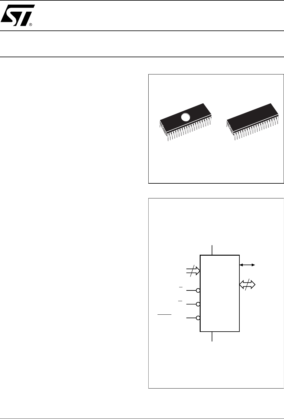
The FDIP40W (window ceramic frit-seal package)
has a transparent lid which allows the user to ex-
pose the chip to ultraviolet light to erase the bit pat-
tern.
A new pattern can then be written rapidly to the de-
vice by following the programming procedure.
For applications where the content is programmed
only one time and erasure is not required, the
M27C400 is offered in PDIP40 package.
1
40
1
40
FDIP40W (F) PDIP40 (B)
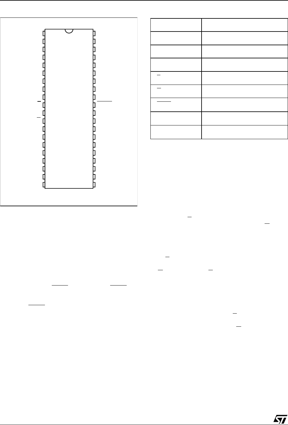
Figure 1. Logic Diagram
AI01634
18
A0-A17
BYTEVPP
Q0-Q14
VCC
M27C400
G
E
VSS
15
Q15A–1
M27C400
2/14
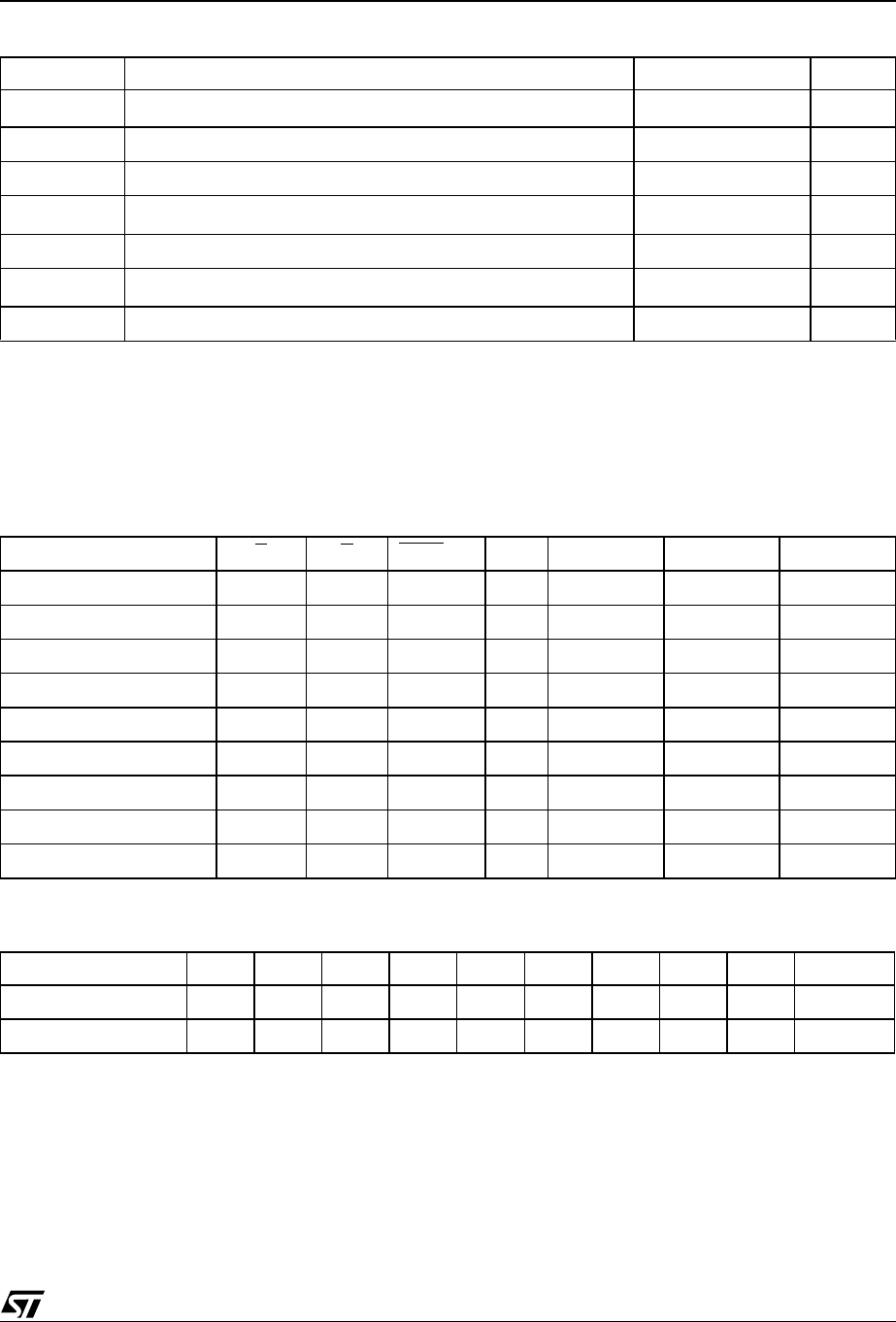
Figure 2. DIP Connections
Q0
Q8
Q1
Q11
A2
VSS
A1
A0
A14
Q15A–1
A15
A16
Q14
A13
BYTEVPP
VSS
Q7
Q12Q10
Q9
VCC
G
Q4
Q6
A10
A9
E
A3
A17 A8
A6
AI01635
M27C400
8
1
2
3
4
5
6
7
9
10
11
12
13
14
15
16
32
31
30
29
28
27
26
25
24
23
22
2120
19
18
17
Q3
Q2
A5
A4
Q13
Q5
40
39
38
37
36
35
34
33
A12
A11
A7
Table 1. Signal Names
A0-A17 Address Inputs
Q0-Q7 Data Outputs
Q8-Q14 Data Outputs
Q15A–1 Data Output / Address Input
EChip Enable
GOutput Enable
BYTEVPP Byte Mode / Program Supply
VCC Supply Voltage
VSS Ground
DEVICE OPERATION
The operating modes of the M27C400 are listed in
the Operating Modes Table. A single power supply
is required in the read mode. All inputs are TTL
compatible except for VPP and 12V on A9 for the
Electronic Signature.
Read Mode
The M27C400 has two organisations, Word-wide
and Byte-wide. The organisation is selected by the
signal level on the BYTEVPP pin. When BYTEVPP
is at VIH the Word-wide organisation is selected
and the Q15A–1 pin is used for Q15 Data Output.
When the BYTEVPP pin is at VIL the Byte-wide or-
ganisation is selected and the Q15A–1 pin is used
for the Address Input A–1. When the memory is
logically regarded as 16 bit wide, but read in the
Byte-wide organisation, then with A–1 at VIL the
lower 8 bits of the 16 bit data are selected and with
A–1 at VIH the upper 8 bits of the 16 bit data are
selected.
The M27C400 has two control functions, both of
which must be logically active in order to obtain
data at the outputs. In addition the Word-wide or
Byte- wide organisation must be selected.
Chip Enable (E) is the power control and should be
used for device selection. Output Enable (G) is the
output control and should be used to gate data to
the output pins independent of device selection.
Assuming that the addresses are stable, the ad-
dress access time (tAVQV) is equal to the delay
from E to output (tELQV). Data is available at the
output after a delay of tGLQV from the falling edge
of G, assuming that E has been low and the ad-
dresses have been stable for at least tAVQV-tGLQV.
Standby Mode
The M27C400 has a standby mode which reduces
the supply current from 50mA to 100µA. The
M27C400 is placed in the standby mode by apply-
ing a CMOS high signal to the E input. When in the
standby mode, the outputs are in a high imped-
ance state, independent of the G input.
3/14
M27C400
Table 2. Absolute Maximum Ratings (1)
Note: 1. Except for the rating “Operating Temperature Range”, stresses above those listed in the Table “Absolute Maximum Ratings” may
cause permanent damage to the device. These are stress ratings only and operation of the device at these or any other conditions
above those indicated in the Operating sections of this specification is not implied. Exposure to Absolute Maximum Rating condi-
tions for extended periods may affect device reliability. Refer also to the STMicroelectronics SURE Program and other relevant qual-
ity documents.
2. Minimum DC voltage on Input or Output is –0.5V with possible undershoot to –2.0V for a period less than 20ns. Maximum DC
voltage on Output is VCC +0.5V with possible overshoot to VCC +2V for a period less than 20ns.
3. Depends on range.
Table 3. Operating Modes
Note: X = VIH or VIL, VID = 12V ± 0.5V.
Table 4. Electronic Signature
Note: Outputs Q15-Q8 are set to '0'.
Symbol Parameter Value Unit
TAAmbient Operating Temperature (3) –40 to 125 °C
TBIAS Temperature Under Bias –50 to 125 °C
TSTG Storage Temperature –65 to 150 °C
VIO (2) Input or Output Voltage (except A9) –2 to 7 V
VCC Supply Voltage –2 to 7 V
VA9 (2) A9 Voltage –2 to 13.5 V
VPP Program Supply Voltage –2 to 14 V
Mode E GBYTEVPP A9 Q7-Q0 Q14-Q8 Q15A–1
Read Word-wide VIL VIL VIH X Data Out Data Out Data Out
Read Byte-wide Upper VIL VIL VIL X Data Out Hi-Z VIH
Read Byte-wide Lower VIL VIL VIL X Data Out Hi-Z VIL
Output Disable VIL VIH X X Hi-Z Hi-Z Hi-Z
Program VIL Pulse VIH VPP X Data In Data In Data In
Verify VIH VIL VPP X Data Out Data Out Data Out
Program Inhibit VIH VIH VPP X Hi-Z Hi-Z Hi-Z
Standby VIH X X X Hi-Z Hi-Z Hi-Z
Electronic Signature VIL VIL VIH VID Codes Codes Code
Identifier A0 Q7 Q6 Q5 Q4 Q3 Q2 Q1 Q0 Hex Data
Manufacturer’s Code VIL 00100000 20h
Device Code VIH 10110010 B2h
M27C400
4/14
Two Line Output Control
Because EPROMs are usually used in larger
memory arrays, this product features a 2-line con-
trol function which accommodates the use of mul-
tiple memory connection. The two-line control
function allows:
a. the lowest possible memory power dissipation
b. complete assurance that output bus contention
will not occur.
For the most efficient use of these two control
lines, E should be decoded and used as the prima-
ry device selecting function, while G should be
made a common connection to all devices in the
array and connected to the READ line from the
system control bus. This ensures that all deselect-
ed memory devices are in their low power standby
mode and that the output pins are only active
when data is required from a particular memory
device.
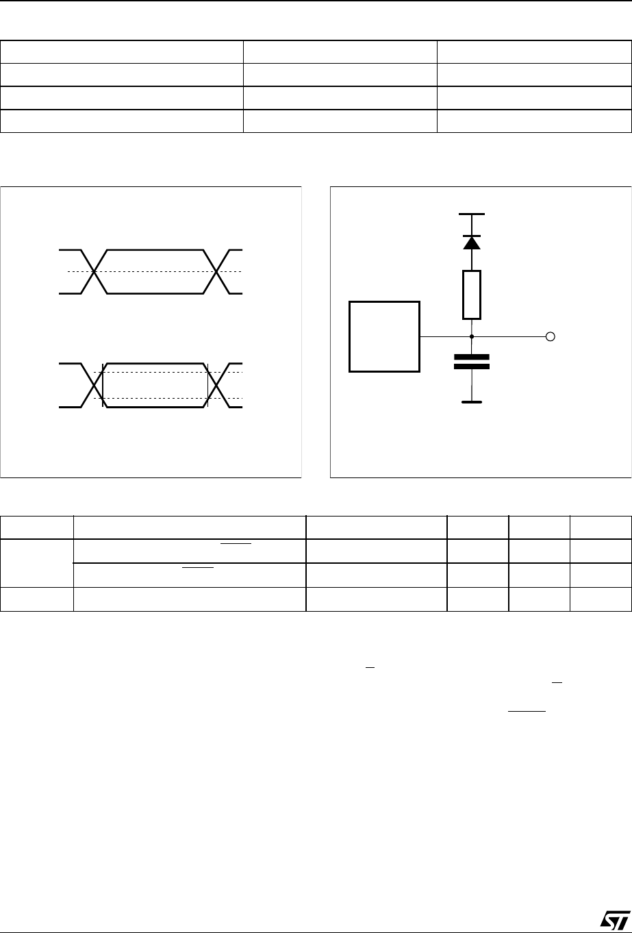
Table 5. AC Measurement Conditions
High Speed Standard
Input Rise and Fall Times ≤ 10ns ≤ 20ns
Input Pulse Voltages 0 to 3V 0.4V to 2.4V
Input and Output Timing Ref. Voltages 1.5V 0.8V and 2V
Figure 3. Testing Input Output Waveform
AI01822
3V
High Speed
0V
1.5V
2.4V
Standard
0.4V
2.0V
0.8V
Figure 4. AC Testing Load Circuit
AI01823B
1.3V
OUT
CL
CL = 30pF for High Speed
CL = 100pF for Standard
CL includes JIG capacitance
3.3kΩ
1N914
DEVICE
UNDER
TEST
Table 6. Capacitance (1) (TA = 25 °C, f = 1 MHz)
Note: 1. Sampled only, not 100% tested.
Symbol Parameter Test Condition Min Max Unit
CIN
Input Capacitance (except BYTEVPP)V
IN = 0V 10 pF
Input Capacitance (BYTEVPP)V
IN = 0V 120 pF
COUT Output Capacitance VOUT = 0V 12 pF
5/14
M27C400
Table 7. Read Mode DC Characteristics (1)
(TA = 0 to 70 °C or –40 to 85 °C; VCC = 5V ± 5% or 5V ± 10%; VPP = VCC)
Note: 1. VCC must be applied simultaneously with or before VPP and removed simultaneously or after VPP.
2. Maximum DC voltage on Output is VCC +0.5V.
Symbol Parameter Test Condition Min Max Unit
ILI Input Leakage Current 0V ≤ VIN ≤ VCC ±1 µA
ILO Output Leakage Current 0V ≤ VOUT ≤ VCC ±10 µA
ICC Supply Current
E = VIL, G = VIL,
IOUT = 0mA, f = 8MHz 70 mA
E = VIL, G = VIL,
IOUT = 0mA, f = 5MHz 50 mA
ICC1 Supply Current (Standby) TTL E = VIH 1mA
I
CC2 Supply Current (Standby) CMOS E > VCC – 0.2V 100 µA
IPP Program Current VPP = VCC 10 µA
VIL Input Low Voltage –0.3 0.8 V
VIH (2) Input High Voltage 2 VCC + 1 V
VOL Output Low Voltage IOL = 2.1mA 0.4 V
VOH Output High Voltage TTL IOH = –400µA 2.4 V
System Considerations
The power switching characteristics of Advanced
CMOS EPROMs require careful decoupling of the
supplies to the devices. The supply current ICC
has three segments of importance to the system
designer: the standby current, the active current
and the transient peaks that are produced by the
falling and rising edges of E. The magnitude of the
transient current peaks is dependent on the ca-
pacitive and inductive loading of the device out-
puts. The associated transient voltage peaks can
be suppressed by complying with the two line out-
put control and by properly selected decoupling
capacitors. It is recommended that a 0.1µF ceram-
ic capacitor is used on every device between VCC
and VSS. This should be a high frequency type of
low inherent inductance and should be placed as
close as possible to the device. In addition, a
4.7µF electrolytic capacitor should be used be-
tween VCC and VSS for every eight devices. This
capacitor should be mounted near the power sup-
ply connection point. The purpose of this capacitor
is to overcome the voltage drop caused by the in-
ductive effects of PCB traces.
Programming
When delivered (and after each erasure for UV
EPROM), all bits of the M27C400 are in the '1'
state. Data is introduced by selectively program-
ming '0's into the desired bit locations. Although
only '0's will be programmed, both '1's and '0's can
be present in the data word. The only way to
change a '0' to a '1' is by die exposition to ultravio-
let light (UVEPROM). The M27C400 is in the pro-
gramming mode when VPP input is at 12.5V, G is
at VIH and E is pulsed to VIL. The data to be pro-
grammed is applied to 16 bits in parallel to the data
output pins. The levels required for the address
and data inputs are TTL. VCC is specified to be
6.25V ± 0.25V.
M27C400
6/14
Table 8A. Read Mode AC Characteristics (1)
(TA = 0 to 70 °C or –40 to 85 °C; VCC = 5V ± 5% or 5V ± 10%; VPP = VCC)
Note: 1. VCC must be applied simultaneously with or before VPP and removed simultaneously or after VPP
2. Sampled only, not 100% tested.
3. Speed obtained with High Speed measurement conditions.
Table 8B. Read Mode AC Characteristics (1)
(TA = 0 to 70 °C or –40 to 85 °C; VCC = 5V ± 5% or 5V ± 10%; VPP = VCC)
Note: 1. VCC must be applied simultaneously with or before VPP and removed simultaneously or after VPP
2. Sampled only, not 100% tested.
Symbol Alt Parameter Test Condition
M27C400
Unit
-55 (3) -70
Min Max Min Max
tAVQV tACC Address Valid to Output Valid E = VIL, G = VIL 55 70 ns
tBHQV tST BYTE High to Output Valid E = VIL, G = VIL 55 70 ns
tELQV tCE Chip Enable Low to Output Valid G = VIL 55 70 ns
tGLQV tOE Output Enable Low to Output Valid E = VIL 30 35 ns
tBLQZ (2) tSTD BYTE Low to Output Hi-Z E = VIL, G = VIL 30 30 ns
tEHQZ (2) tDF Chip Enable High to Output Hi-Z G = VIL 0 30 0 30 ns
tGHQZ (2) tDF Output Enable High to Output Hi-Z E = VIL 0 30 0 30 ns
tAXQX tOH Address Transition to Output Transition E = VIL, G = VIL 55ns
t
BLQX tOH BYTE Low to Output Transition E = VIL, G = VIL 55ns
Symbol Alt Parameter Test Condition
M27C400
Unit-80 -100
Min Max Min Max
tAVQV tACC Address Valid to Output Valid E = VIL, G = VIL 80 100 ns
tBHQV tST BYTE High to Output Valid E = VIL, G = VIL 80 100 ns
tELQV tCE Chip Enable Low to Output Valid G = VIL 80 100 ns
tGLQV tOE Output Enable Low to Output Valid E = VIL 40 50 ns
tBLQZ (2) tSTD BYTE Low to Output Hi-Z E = VIL, G = VIL 40 50 ns
tEHQZ (2) tDF Chip Enable High to Output Hi-Z G = VIL 0 40 0 50 ns
tGHQZ (2) tDF Output Enable High to Output Hi-Z E = VIL 0 40 0 50 ns
tAXQX tOH Address Transition to Output Transition E = VIL, G = VIL 55ns
t
BLQX tOH BYTE Low to Output Transition E = VIL, G = VIL 55ns
7/14
M27C400
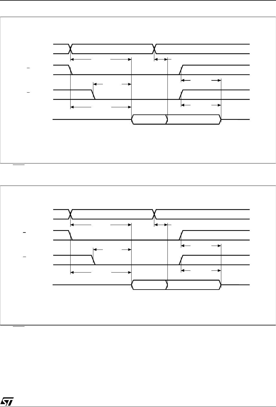
Figure 5. Word-Wide Read Mode AC Waveforms
Note: BYTEVPP = VIH.
Figure 6. Byte-Wide Read Mode AC Waveforms
Note: BYTEVPP = VIL.
AI01636
tAXQX
tEHQZ
A0-A17
E
G
Q0-Q15
tAVQV
tGHQZ
tGLQV
tELQV
VALID
Hi-Z
VALID
AI01637
tAXQX
tEHQZ
A–1,A0-A17
E
G
Q0-Q7
tAVQV
tGHQZ
tGLQV
tELQV
VALID
Hi-Z
VALID
M27C400
8/14
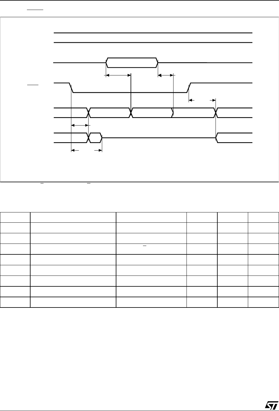
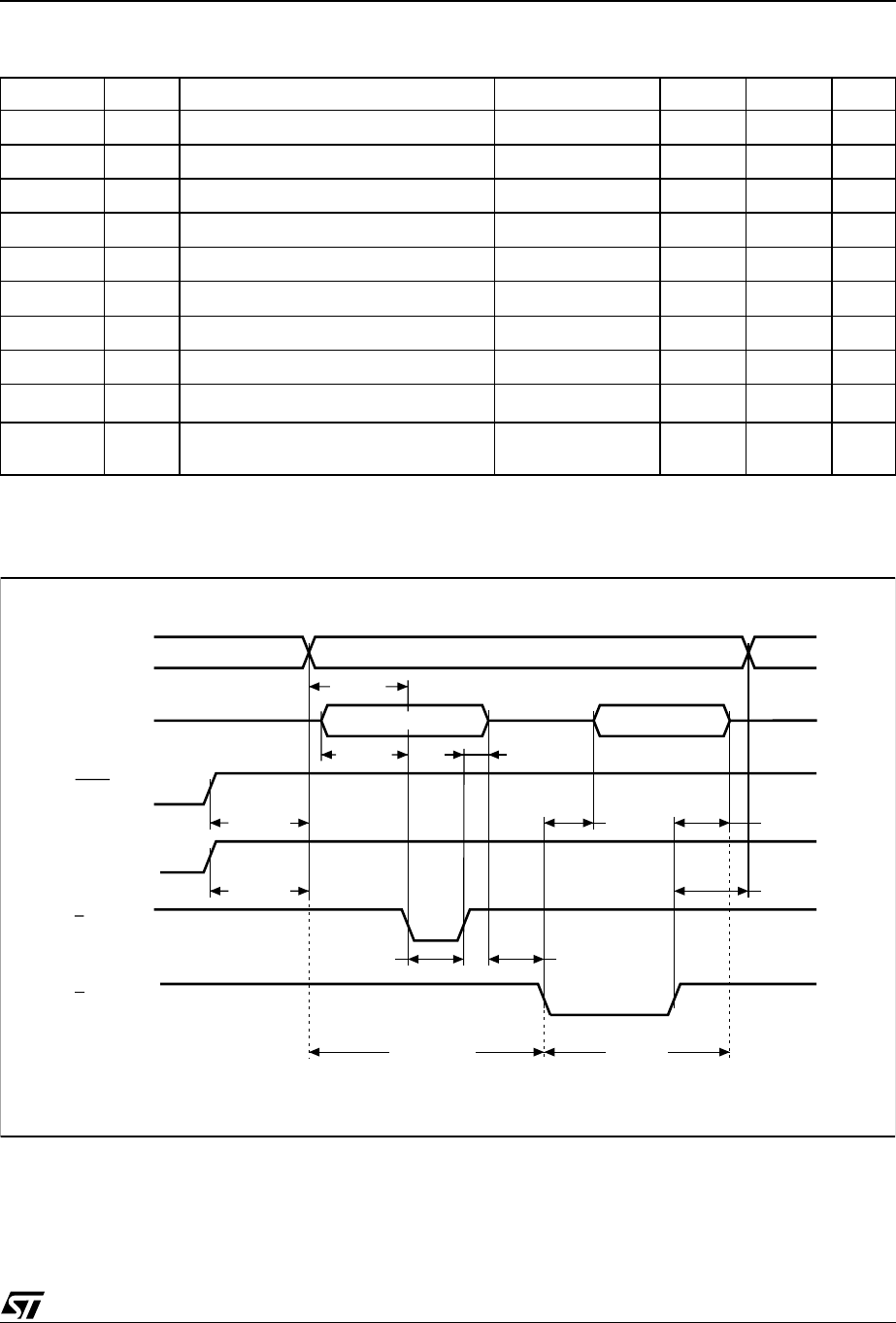
Figure 7. BYTE Transition AC Waveforms
Note: Chip Enable (E) and Output Enable (G) = VIL.
AI01638B
tAXQX
tBHQV
A0-A17
BYTEVPP
tAVQV
tBLQX
tBLQZ
VALID
Hi-Z
A–1
DATA OUT
DATA OUT
VALID
Q0-Q7
Q8-Q15
Table 9. Programming Mode DC Characteristics (1)
(TA = 25 °C; VCC = 6.25V ± 0.25V; VPP = 12.5V ± 0.25V)
Note: 1. VCC must be applied simultaneously with or before VPP and removed simultaneously or after VPP.
Symbol Parameter Test Condition Min Max Unit
ILI Input Leakage Current 0 ≤ VIN ≤ VCC ±1 µA
ICC Supply Current 50 mA
IPP Program Current E = VIL 50 mA
VIL Input Low Voltage –0.3 0.8 V
VIH Input High Voltage 2.4 VCC + 0.5 V
VOL Output Low Voltage IOL = 2.1mA 0.4 V
VOH Output High Voltage TTL IOH = –2.5mA 3.5 V
VID A9 Voltage 11.5 12.5 V
9/14
M27C400
Table 10. Programming Mode AC Characteristics (1)
(TA = 25 °C; VCC = 6.25V ± 0.25V; VPP = 12.5V ± 0.25V)
Note: 1. VCC must be applied simultaneously with or before VPP and removed simultaneously or after VPP.
2. Sampled only, not 100% tested.
Symbol Alt Parameter Test Condition Min Max Unit
tAVEL tAS Address Valid to Chip Enable Low 2 µs
tQVEL tDS Input Valid to Chip Enable Low 2 µs
tVPHAV tVPS VPP High to Address Valid 2µs
t
VCHAV tVCS VCC High to Address Valid 2µs
t
ELEH tPW Chip Enable Program Pulse Width 45 55 µs
tEHQX tDH Chip Enable High to Input Transition 2 µs
tQXGL tOES Input Transition to Output Enable Low 2 µs
tGLQV tOE Output Enable Low to Output Valid 120 ns
tGHQZ (2) tDFP Output Enable High to Output Hi-Z 0 130 ns
tGHAX tAH Output Enable High to Address
Transition 0ns
Figure 8. Programming and Verify Modes AC Waveforms
tAVEL
VALID
AI01639
A0-A17
Q0-Q15
BYTEVPP
VCC
G
DATA IN DATA OUT
E
tQVEL
tVPHAV
tVCHAV
tEHQX
tELEH
tGLQV
tQXGL
tGHQZ
tGHAX
PROGRAM VERIFY
M27C400
10/14
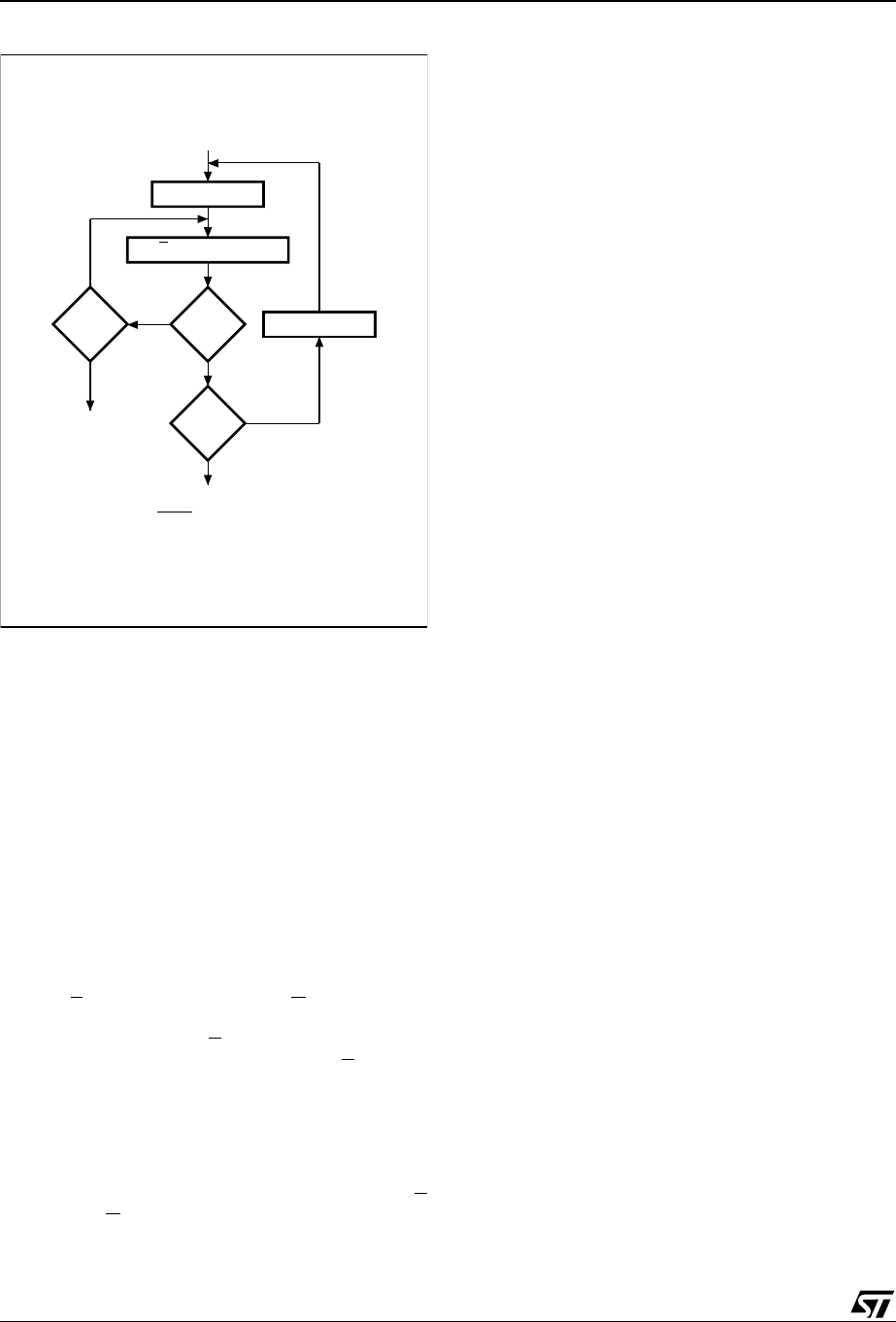
Figure 9. Programming Flowchart
AI01044B
n = 0
Last
Addr
VERIFY
E = 50µs Pulse
++n
= 25 ++ Addr
VCC = 6.25V, VPP = 12.5V
FAIL
CHECK ALL WORDS
BYTEVPP =VIH
1st: VCC = 6V
2nd: VCC = 4.2V
YES
NO
YES
NO
YES
NO
PRESTO III Programming Algorithm
The PRESTO III Programming Algorithm allows
the whole array to be programed with a guaran-
teed margin in a typical time of 26 seconds. Pro-
gramming with PRESTO III consists of applying a
sequence of 50µs program pulses to each word
until a correct verify occurs (see Figure 9). During
programing and verify operation a MARGIN
MODE circuit is automatically activated to guaran-
tee that each cell is programed with enough mar-
gin. No overpromise pulse is applied since the
verify in MARGIN MODE provides the necessary
margin to each programmed cell.
Program Inhibit
Programming of multiple M27C400s in parallel
with different data is also easily accomplished. Ex-
cept for E, all like inputs including G of the parallel
M27C400 may be common. A TTL low level pulse
applied to a M27C400's E input and VPP at 12.5V,
will program that M27C400. A high level E input in-
hibits the other M27C400s from being pro-
grammed.
Program Verify
A verify (read) should be performed on the pro-
grammed bits to determine that they were correct-
ly programmed. The verify is accomplished with E
at VIH and G at VIL, VPP at 12.5V and VCC at
6.25V.
On-Board Programming
The M27C400 can be directly programmed in the
application circuit. See the relevant Application
Note AN620.
Electronic Signature
The Electronic Signature (ES) mode allows the
reading out of a binary code from an EPROM that
will identify its manufacturer and type. This mode
is intended for use by programming equipment to
automatically match the device to be programmed
with its corresponding programming algorithm.
The ES mode is functional in the 25°C ± 5°C am-
bient temperature range that is required when pro-
gramming the M27C400. To activate the ES
mode, the programming equipment must force
11.5V to 12.5V on address line A9 of the
M27C400, with VPP =V
CC = 5V. Two identifier
bytes may then be sequenced from the device out-
puts by toggling address line A0 from VIL to VIH. All
other address lines must be held at VIL during
Electronic Signature mode.
Byte 0 (A0 = VIL) represents the manufacturer
code and byte 1 (A0 = VIH) the device identifier
code. For the STMicroelectronics M27C400, these
two identifier bytes are given in Table 4 and can be
read-out on outputs Q7 to Q0.
ERASURE OPERATION (applies to UV EPROM)
The erasure characteristics of the M27C400 is
such that erasure begins when the cells are ex-
posed to light with wavelengths shorter than ap-
proximately 4000 Å. It should be noted that
sunlight and some type of fluorescent lamps have
wavelengths in the 3000-4000 Å range. Research
shows that constant exposure to room level fluo-
rescent lighting could erase a typical M27C400 in
about 3 years, while it would take approximately 1
week to cause erasure when exposed to direct
sunlight. If the M27C400 is to be exposed to these
types of lighting conditions for extended periods of
time, it is suggested that opaque labels be put over
the M27C400 window to prevent unintentional era-
sure. The recommended erasure procedure for
M27C400 is exposure to short wave ultraviolet
light which has a wavelength of 2537 Å. The inte-
grated dose (i.e. UV intensity x exposure time) for
erasure should be a minimum of 30 W-sec/cm2.
The erasure time with this dosage is approximate-
ly 30 to 40 minutes using an ultraviolet lamp with
12000 µW/cm2 power rating. The M27C400
should be placed within 2.5cm (1 inch) of the lamp
tubes during the erasure. Some lamps have a filter
on their tubes which should be removed before
erasure.

11/14
M27C400
Table 11. Ordering Information Scheme
Note: 1. High Speed, see AC Characteristics section for further information.
For a list of available options (Speed, Package, etc...) or for further information on any aspect of this de-
vice, please contact the STMicroelectronics Sales Office nearest to you.
Example: M27C400 -70 X F 1 TR
Device Type
M27
Supply Voltage
C = 5V
Device Function
400 = 4 Mbit (512Kb x8 or 256Kb x16)
Speed
-55 (1) = 55 ns
-70 = 70 ns
-80 = 80 ns
-100 = 100 ns
VCC Tolerance
blank = ± 10%
X = ± 5%
Package
F = FDIP40W
B = PDIP40
Temperature Range
1 = 0 to 70 °C
6 = –40 to 85 °C
Options
TR = Tape & Reel Packing
M27C400
12/14
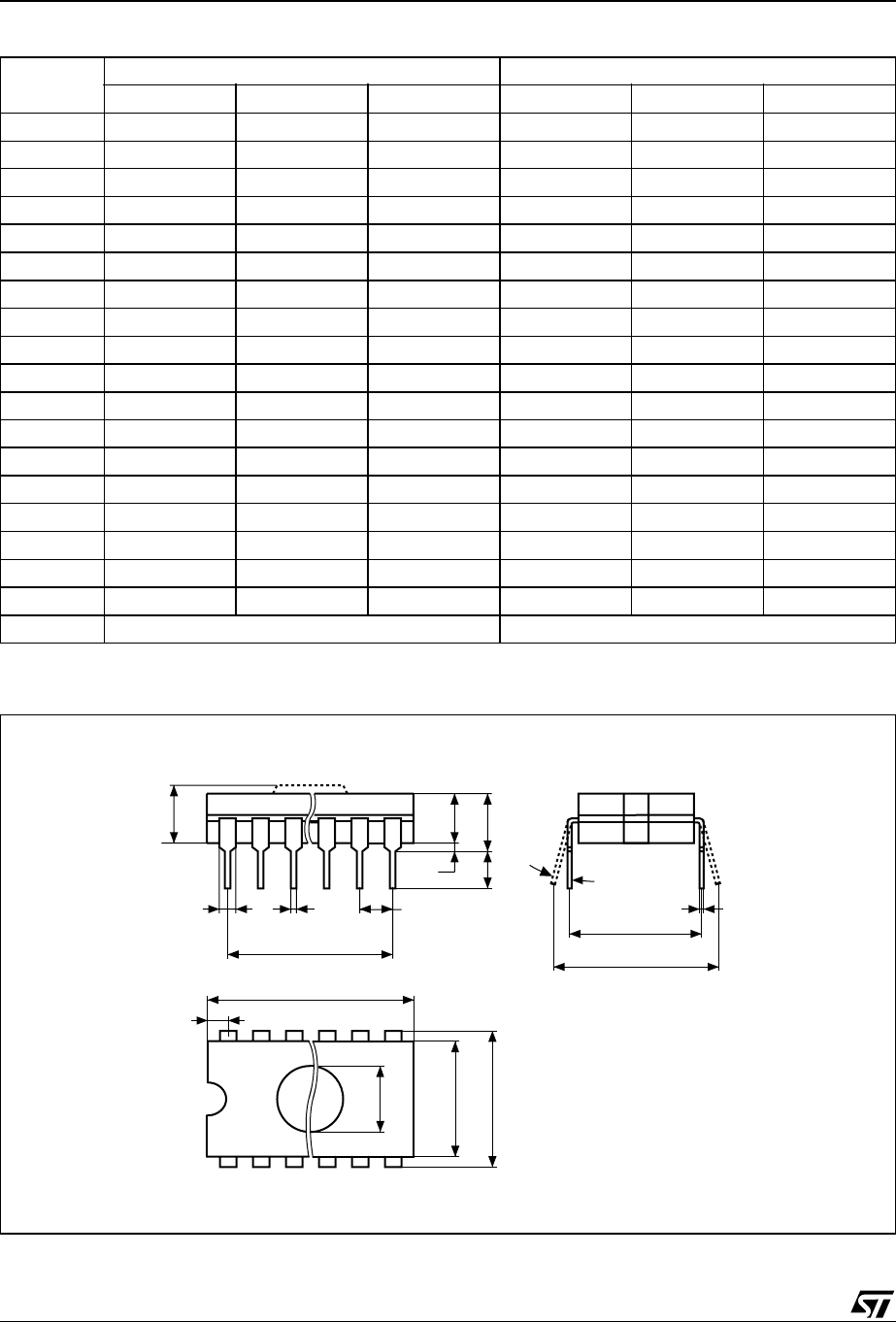
Table 12. FDIP40W - 40 lead Ceramic Frit-seal DIP with window, Package Mechanical Data
Symb mm inches
Typ Min Max Typ Min Max
A 5.72 0.225
A1 0.51 1.40 0.020 0.055
A2 3.91 4.57 0.154 0.180
A3 3.89 4.50 0.153 0.177
B 0.41 0.56 0.016 0.022
B1 1.45 – – 0.057 – –
C 0.23 0.30 0.009 0.012
D 51.79 52.60 2.039 2.071
D2 48.26 – – 1.900 – –
E 15.24 – – 0.600 – –
E1 13.06 13.36 0.514 0.526
e 2.54 – – 0.100 – –
ea. 14.99 – – 0.590 – –
be 16.18 18.03 0.637 0.710
L 3.18 – 0.125 –
S 1.52 2.49 0.060 0.098
∅8.13 – – 0.320 – –
α4° 11° 4° 11°
N40 40
Figure 10. FDIP40W - 40 lead Ceramic Frit-seal DIP with window, Package Outline
Drawing is not to scale.
FDIPW-a
A3
A1
A
L
B1 B e
D
S
E1 E
N
1
C
α
eA
D2
∅
eB
A2
13/14
M27C400
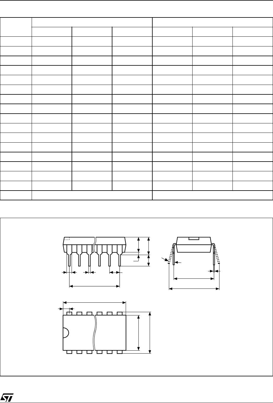
Table 13. PDIP40 - 40 pin Plastic DIP, 600 mils width, Package Mechanical Data
Symb mm inches
Typ Min Max Typ Min Max
A4.45 – – 0.175 – –
A1 0.64 0.38 – 0.025 0.015 –
A2 3.56 3.91 0.140 0.154
B 0.38 0.53 0.015 0.021
B1 1.14 1.78 0.045 0.070
C 0.20 0.31 0.008 0.012
D 51.78 52.58 2.039 2.070
D2 48.26 – – 1.900 – –
E 14.80 16.26 0.583 0.640
E1 13.46 13.99 0.530 0.551
e1 2.54 – – 0.100 – –
ea. 15.24 – – 0.600 –
be 15.24 17.78 0.600 0.700
L 3.05 3.81 0.120 0.150
S 1.52 2.29 0.060 0.090
α0° 15° 0° 15°
N40 40
Figure 11. PDIP40 - 40 lead Plastic DIP, 600 mils width, Package Outline
Drawing is not to scale.
PDIP
A2
A1
A
L
B1 B e1
D
S
E1 E
N
1
C
α
eA
eB
D2

M27C400
14/14
Information furnished is believed to be accurate and reliable. However, STMicroelectronics assumes no responsibility for the consequences
of use of such information nor for any infringement of patents or other rights of third parties which may result from its use. No license is granted
by implication or otherwise under any patent or patent rights of STMicroelectronics. Specifications mentioned in this publication are subject
to change without notice. This publication supersedes and replaces all information previously supplied. STMicroelectronics products are not
authorized for use as critical components in life support devices or systems without express written approval of STMicroelectronics.
The ST logo is registered trademark of STMicroelectronics
1999 STMicroelectronics - All Rights Reserved
All other names are the property of their respective owners.
STMicroelectronics GROUP OF COMPANIES
Australia - Brazil - Canada - China - France - Germany - Italy - Japan - Korea - Malaysia - Malta - Mexico - Morocco - The Netherlands -
Singapore - Spain - Sweden - Switzerland - Taiwan - Thailand - United Kingdom - U.S.A.
http://www.st.com
