2N4117A, 2N4118A, 2N4119A, PN4117A, PN4118A, PN4119A, SST4117, SST4118, SST4119 Datasheet. Www.s Manuals.com. Vishay
User Manual: Marking of electronic components, SMD Codes T7, T7***, T7-, T7W, T7p, T7t, t70, t71, t72, t73, t74, t75, t7C, t7F, t7R, t7T, t7V, t7X. Datasheets 2N7002F, APX824-26W5, BSR15, BZX384-C3V6, BZX84-A27, BZX84-B16, BZX84-B18, BZX84-B20, BZX84-B22, BZX84-B24, PDTA115EU, PDTD113ET, PDTD113ZT, PDTD123ET, PDTD123YT, SST4117, ZUMT817-25.
Open the PDF directly: View PDF ![]() .
.
Page Count: 6
2N/PN/SST4117A Series
Vishay Siliconix
Document Number: 70239
S-41231—Rev. G, 28-Jun-04
www.vishay.com
1
N-Channel JFETs
2N4117A PN4117A SST4117
2N4118A PN4118A SST4118
2N4119A PN4119A SST4119
PRODUCT SUMMARY
Part Number VGS(off) (V) V(BR)GSS Min (V) gfs Min (mS) IDSS Min (mA)
4117 −0.6 to −1.8 −40 70 30
4118 −1 to −3−40 80 80
4119 −2 to −6−40 100 200
FEATURES BENEFITS APPLICATIONS
DUltra-Low Leakage: 0.2 pA
DVery Low Current/Voltage Operation
DUltrahigh Input Impedance
DLow Noise
DInsignificant Signal Loss/Error Voltage
with High-Impedance Source
DLow Power Consumption (Battery)
DMaximum Signal Output, Low Noise
DHigh Sensitivity to Low-Level Signals
DHigh-Impedance Transducer
Amplifiers
DSmoke Detector Input
DInfrared Detector Amplifier
DPrecision Test Equipment
DESCRIPTION
The 2N/PN/SST4117A series of n-channel JFETs provide
ultra-high input impedance. These devices are specified with
a 1-pA limit and typically operate at 0.2 pA. This makes them
perfect choices for use as high-impedance sensitive front-end
amplifiers.
The hermetically sealed TO-206AF package allows full
military processing per MIL-S-19500 (see Military
Information). The TO-226A (TO-92) plastic package provides
a low-cost option. The TO-236 (SOT-23) package provides
surface-mount capability. Both the PN and SST series are
available in tape-and-reel for automated assembly (see
Packaging Information).
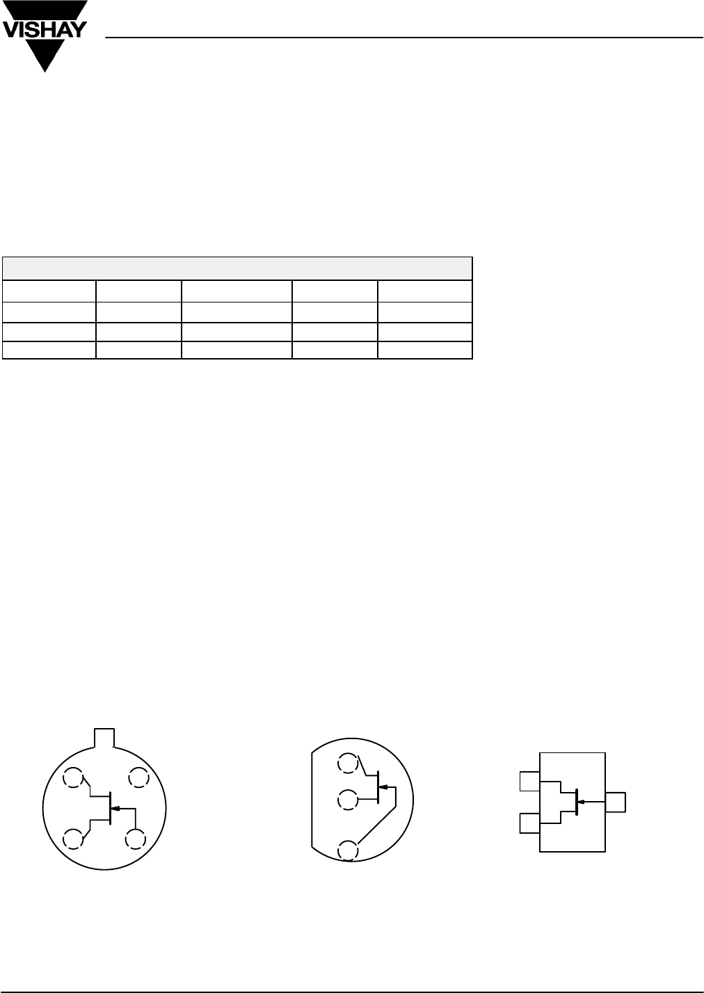
G
S
TO-206AF
(TO-72)
D
Top View
2N4117A
2N4118A
2N4119A
C
1
23
4
D
G
Top View
PN4117A
PN4118A
PN4119A
TO-226AA
(TO-92)
S
1
2
3
D
S
G
TO-236
(SOT-23)
2
3
1
Top View
SST4117 (T7)*
SST4118 (T8)*
SST4119 (T9)*
*Marking Code for TO-236
For applications information see AN105.
2N/PN/SST4117A Series
Vishay Siliconix
www.vishay.com
2
Document Number: 70239
S-41231—Rev. G, 28-Jun-04
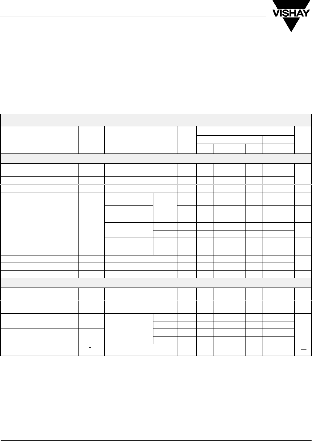
ABSOLUTE MAXIMUM RATINGS
Gate-Source/Gate-Drain Voltage −40V. . . . . . . . . . . . . . . . . . . . . . . . . . . . . . . .
Forward Gate Current 50 mA. . . . . . . . . . . . . . . . . . . . . . . . . . . . . . . . . . . . . . . . .
Storage Temperature : (2N Prefix) −65 to 175_C. . . . . . . . . . . . . . . . . . .
(PN, SST Prefix) −55 to 150_C. . . . . . . . . . . . .
Operating Junction Temperature :
(2N Prefix) −55 to 175_C. . . . . . . . . . . . . . . . . . .
(PN, SST Prefix) −55 to 150_C. . . . . . . . . . . . .
Lead Temperature (1/16” from case for 10 sec.) 300_C. . . . . . . . . . . . . . . . . . .
Power Dissipation (case 25_C) :
(2N Prefix)a300 mW. . . . . . . . . . . . . . . . . . . . . .
(PN, SST Prefix)b350 mW. . . . . . . . . . . . . . . .
Notes
a. Derate 2 mW/_C above 25_C
b. Derate 2.8 mW/_C above 25_C
SPECIFICATIONS (TA = 25_C UNLESS OTHERWISE NOTED)
Limits
4117 4118 4119
Parameter Symbol Test Conditions TypaMin Max Min Max Min Max Unit
Static
Gate-Source
Breakdown Voltage V(BR)GSS IG = −1 mA , VDS = 0 V −70 −40 −40 −40 V
Gate-Source Cutoff Voltage VGS(off) VDS = 10 V, ID = 1 nA −0.6 −1.8 −1−3−2−6
V
Saturation Drain Current IDSS VDS = 10 V, VGS = 0 V 30 90 80 240 200 600 mA
VGS = −20 V
VDS = 0 V −0.2 −1−1−1 pA
Gt R C t
I
VGS = −20 V
VDS = 0 V
TA = 150_C
2N
−0.4 −2.5 −2.5 −2.5 nA
Gate Reverse Current IGSS V
GS
= −10 V PN −0.2 −1−1−1
pA
VGS = −10 V
VDS = 0 V SST −0.2 −10 −10 −10 pA
VGS = −10 V
VDS = 0 V
TA = 100_C
PN/SST −0.03 −2.5 −2.5 −2.5 nA
Gate Operating CurrentbIGVDG = 15 V, ID = 30 mA−0.2
pA
Drain Cutoff CurrentbID(off) VDS = 10 V, VGS = −8 V 0.2 pA
Gate-Source Forward VoltagebVGS(F) IG = 1 mA , VDS = 0 V 0.7 V
Dynamic
Common-Source
Forward Transconductance gfs VD
S
= 10 V, V
GS
= 0 V 70 210 80 250 100 330
mS
Common-Source
Output Conductance gos
VDS = 10 V
,
VGS = 0 V
f = 1 kHz 3 5 10
mS
Common-Source
Ci
2N/PN 1.2 3 3 3
Common-Source
Input Capacitance Ciss VDS = 10 V
VGS = 0 V
SST 1.2
pF
Common-Source
C
VGS = 0 V
f = 1 MHz 2N/PN 0.3 1.5 1.5 1.5 pF
Common-Source
Reverse Transfer Capacitance Crss
f = 1 MHz
SST 0.3
Equivalent Input Noise VoltagebenVDS = 10 V, VGS = 0 V
f = 1 kHz 15 nV⁄
√Hz
Notes
a. Typical values are for DESIGN AID ONLY, not guaranteed nor subject to production testing. NT
b. This parameter not registered with JEDEC.
2N/PN/SST4117A Series
Vishay Siliconix
Document Number: 70239
S-41231—Rev. G, 28-Jun-04
www.vishay.com
3
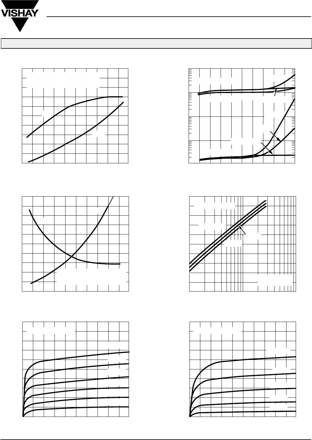
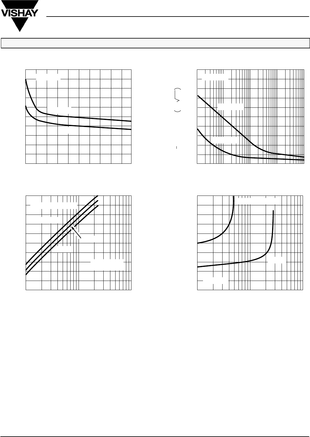
TYPICAL CHARACTERISTICS (TA = 25_C UNLESS OTHERWISE NOTED)
Gate Leakage Current
Drain Current and Transconductance
vs. Gate-Source Cutoff Voltage
Common-Source Forward Transconductance
vs. Drain Current
On-Resistance and Output Conductance
vs. Gate-Source Cutoff Voltage
Output Characteristics
1000
0−5−4−3−2−1
800
0
06 30
gfs
IDSS
TA = 25_C
100 mA
IGSS @ 25_C
100 mA
Output Characteristics
500
400
300
100
0
−0.5 V
−1.0 V
−2.0 V
−1.5 V
VGS = 0 V
15
0−3−5−4−2−1
12
9
6
3
0
0.01 0.1 1
200
160
120
40
0
5
4
3
2
1
0
rDS @ ID = 10 mA, VGS = 0 V
gos @ VDS = 10 V, VGS = 0 V
f = 1 kHz
rDS
gos
TA = −55_C
125_C
VDS = 10 V
f = 1 kHz
100
0168420
80
60
20
0
VGS = 0 V
−0.5 V
−0.4 V
−0.3 V
−0.2 V
−0.1 V
VGS(off) − Gate-Source Cutoff Voltage (V)
VDS − Drain-Source Voltage (V)
VDG − Drain-Gate Voltage (V)
ID − Drain Current (mA)VGS(off) − Gate-Source Cutoff Voltage (V)
VDS − Drain-Source Voltage (V)
600
400
200
12 18 24
80
25_C
VGS(off) = −0.7 V VGS(off) = −2.5 V
20040
12 0 16842012
IDSS @ VDS = 10 V, VGS = 0 V
gfs @ VDS = 10 V, VGS = 0 V
f = 1 kHz
300
240
180
120
60
0
10 mA
0.1 pA
1 pA
10 pA
100 pA
1 nA
IGSS @ 125_C
VGS(off) = −2.5 V
10 mA
VGS(off) = −2.5 V
IDSS − Saturation Drain Current (µA)
gfs − Forward Transconductance (µS) gos − Output Conductance (µS)
gfs − Forward Transconductance (µS) IG − Gate Leakage
ID − Drain Current (µA)
ID − Drain Current (µA)
TA = 125_C
rDS(on) − Drain-Source On-Resistance (kW)
2N/PN/SST4117A Series
Vishay Siliconix
www.vishay.com
4
Document Number: 70239
S-41231—Rev. G, 28-Jun-04
TYPICAL CHARACTERISTICS (TA = 25_C UNLESS OTHERWISE NOTED)
300
240
180
60
0
Transconductance vs. Gate-Source VoltageTransfer Characteristics
Transconductance vs. Gate-Source VoltageTransfer Characteristics
Common-Source Input Capacitance
vs. Gate-Source Voltage
Circuit Voltage Gain vs. Drain Current
500
0−4−5−2−1
0
TA = −55_C
125_C
100
0−0.4−0.2 −0.8 −1.0
80
60
20
0
200
160
120
40
0
TA = 125_C
−55_C
TA = −55_C
125_C
VDS = 10 V VDS = 10 V
f = 1 kHz
VDS = 10 V VDS = 10 V
f = 1 kHz
TA = −55_C
125_C
0.1 10.01
100
0
VGS(off) = −0.7 V
−2.5 V
RL+10 V
ID
Assume VDD = 15 V, VDS = 5 V
2.0
0
f = 1 MHz
VDS = 0 V
10 V
VGS − Gate-Source Voltage (V)
ID − Drain Current (mA)
VGS − Gate-Source Voltage (V)
VGS − Gate-Source Voltage (V) VGS − Gate-Source Voltage (V)
VGS − Gate-Source Voltage (V)
VGS(off) = −0.7 V VGS(off) = −0.7 V
VGS(off) = −2.5 V VGS(off) = −2.5 V
40
80
60
20
40
80
25_C
25_C
−0.6 0 −0.4−0.2 −0.8 −1.0−0.6
−30−4−5−2−1−3
0−16 −20−8−4−12
120
400
300
100
200
1.6
1.2
0.4
0.8
AV+
gfs RL
1)RLgos
25_C
25_C
gfs − Forward Transconductance (µS) gfs − Forward Transconductance (µS)
AV − Voltage Gain
Ciss − Input Capacitance (pF)
ID − Drain Current (µA) ID − Drain Current (µA)
2N/PN/SST4117A Series
Vishay Siliconix
Document Number: 70239
S-41231—Rev. G, 28-Jun-04
www.vishay.com
5
TYPICAL CHARACTERISTICS (TA = 25_C UNLESS OTHERWISE NOTED)
2
1
0
0.01 0.1 1
Equivalent Input Noise Voltage vs. Frequency
ID − Drain Current (mA)
Common-Source Reverse Feedback Capacitance
vs. Gate-Source Voltage
On-Resistance vs. Drain CurrentOutput Conductance vs. Drain Current
VDS = 10 V
f = 1 kHz
0.5
0−8−20−16−4
0.4
0.3
0.1
0
f = 1 MHz
VDS = 0 V
10 V
10 100 1 k
100 k
10 k
200
0
VDS = 10 V
ID = 10 mA
VGS = 0 V
TA = −55_C
125_C
ID − Drain Current (mA)
VGS − Gate-Source Voltage (V) f − Frequency (Hz)
0.2
160
120
40
80
−12
VGS(off) = −2.5 V
20
0
0.01 0.1 1
16
12
8
4
VGS(off) = −0.7 V
−2.5 V
TA = 25_C
25_C
en − Noise Voltage nV / Hz
rDS(on) − Drain-Source On-Resistance ( Ω )
gos − Output Conductance (µS) Crss − Reverse Feedback Capacitance (pF)