2N4391, 2N4392, 2N4393, PN4391, PN4392, PN4393, SST4391, SST4392, SST4393 Datasheet. Www.s Manuals.com. Vishay
User Manual: Marking of electronic components, SMD Codes CA, CA*, CA**, CA***, CA-***, CA=***, CAW, Ca. Datasheets 74AHCT1G00GW, BCX68, BD48E51G, BD48K51G, MAX6314US38D1-T, MMBZ4691-V, MMBZ5257B, RP130Q301A, RT8010PQV, RT9011-SFGJ6, RT9271GE, RT9271PE, SST4391, SY7208, Si1912EDH, TPS61041DRV.
Open the PDF directly: View PDF ![]() .
.
Page Count: 7
2N/PN/SST4391 Series
Vishay Siliconix
Document Number: 70241
S-04028—Rev. F, 04-Jan-01 www.vishay.com
7-1
N-Channel JFETs
2N4391 PN4391 SST4391
2N4392 PN4392 SST4392
2N4393 PN4393 SST4393
PRODUCT SUMMARY
Part Number VGS(off) (V) rDS(on) Max ()ID(off) Typ (pA) tON Typ (ns)
2N/PN/SST4391 –4 to –10 30 5 4
2N/PN/SST4392 –2 to –5 60 5 4
2N/PN/SST4393 –0.5 to –3 100 5 4
FEATURES BENEFITS APPLICATIONS
DLow On-Resistance: 4391<30
DFast Switching—tON: 4 ns
DHigh Off-Isolation: ID(off) with Low
Leakage
DLow Capacitance: < 3.5 pF
DLow Insertion Loss
DLow Error Voltage
DHigh-Speed Analog Circuit Performance
DNegligible “Off-Error,” Excellent Accuracy
DGood Frequency Response, Low Glitches
DEliminates Additional Buffering
DAnalog Switches
DChoppers
DSample-and-Hold
DNormally “On” Switches
DCurrent Limiters
DCommutators
DESCRIPTION
The 2N/PN/SST4391 series features many of the superior
characteristics of JFETs which make it a good choice for
demanding analog switching applications and for specialized
amplifier circuits.
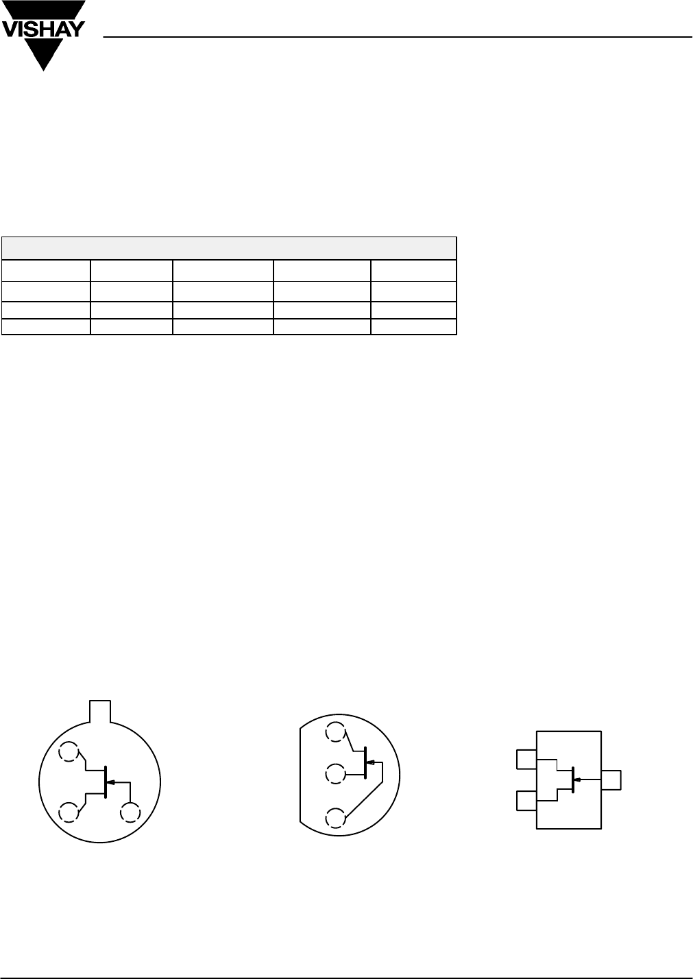
The 2N series hermetically-sealed TO-206AA (TO-18) can is
available with processing per MIL-S-19500 (see Military
Information). Both the PN, TO-226AA (TO-92), and SST,
TO-236 (SOT-23), series are available in tape-and-reel for
automated assembly (see Packaging Information). For similar
dual products, see the 2N5564/5565/5566 data sheet.
D
S
G and Case
TO-206AA
(TO-18)
Top View
2N4391
2N4392
2N4393
1
23
TO-226AA
(TO-92)
Top View
PN4391
PN4392
PN4393
D
G
S
1
2
3
D
S
G
TO-236
(SOT-23)
2
3
1
Top View
SST4391 (CA)*
SST4392 (CB)*
SST4393 (CC)*
*Marking Code for TO-236
For applications information see AN104 and AN106
.
2N/PN/SST4391 Series
Vishay Siliconix
www.vishay.com
7-2 Document Number: 70241
S-04028—Rev. F, 04-Jan-01
ABSOLUTE MAXIMUM RATINGS
Gate-Drain, Gate-Source Voltage:
(2N/PN Prefixes) –40 V. . . . . . . . . . . . . . . . . . .
(SST Prefix) –35 V. . . . . . . . . . . . . . . . . . . . . . .
Gate Current 50 mA. . . . . . . . . . . . . . . . . . . . . . . . . . . . . . . . . . . . . . . . . . . . . . . . .
Lead Temperature 300 _C. . . . . . . . . . . . . . . . . . . . . . . . . . . . . . . . . . . . . . . . . . .
Storage Temperature : (2N Prefix) –65 to 200 _C. . . . . . . . . . . . . . . . . .
(PN/SST Prefixes) –55 to 150 _C. . . . . . . . . . .
Operating Junction Temperature :
(2N Prefix) –55 to 200 _C. . . . . . . . . . . . . . . . . .
(PN/SST Prefixes) –55 to 150 _C. . . . . . . . . . .
Power Dissipation : (2N Prefix)a(TC = 25_C) 1800 mW. . . . . . . . . .
(PN/SST Prefixes)b350 mW. . . . . . . . . . . . . . .
Notes
a. Derate 10 mW/_C above 25_C
b. Derate 2.8 mW/_C above 25_C
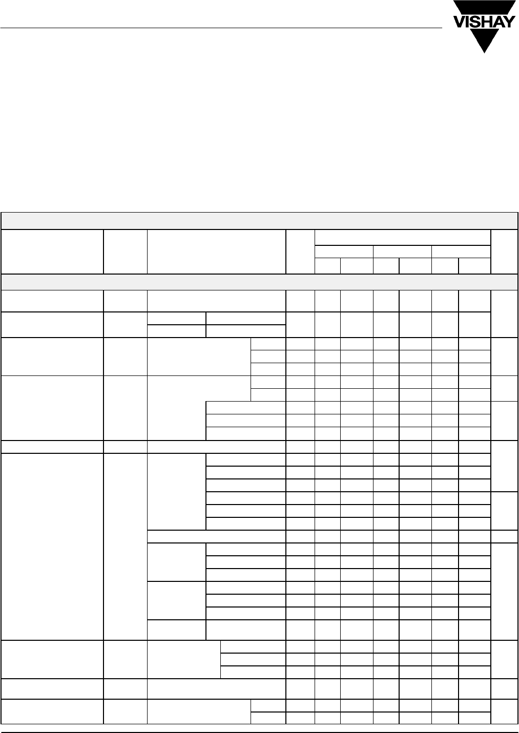
SPECIFICATIONS (TA = 25_C UNLESS OTHERWISE NOTED)
Limits
4391 4392 4393
Parameter Symbol Test Conditions TypaMin Max Min Max Min Max Unit
Static
Gate-Source
Breakdown Voltage V(BR)GSS IG = –1 A, VDS = 0 V –55 –40 –40 –40
Gate-Source VDS = 20 V 2N/PN: ID = 1 nA V
Gate-Source
Cutoff Voltage VGS(off) VDS = 15 V SST: ID = 10 nA –4–10 –2–5–0.5 –3
2N 50 150 25 75 5 30
Saturation Drain
CurrentbIDSS VDS = 20 V, VGS = 0 V PN 50 150 25 100 5 60 mA
CurrentbDSS DS GS
SST 50 25 5
VGS = –20 V 2N/SST –5–100 –100 –100
VGS = –20 V
VDS = 0 V PN –5–1000 –1000 –1000 pA
Gate Reverse Current IGSS 2N: TA = 150_C–13 –200 –200 –200
GSS
PN: TA = 100_C–1–200 –200 –200 nA
SST: TA = 125_C–3
Gate Operating Current IGVDG = 15 V, ID = 10 mA –5
2N: VGS = –5 V 5 100
2N: VGS = –7 V 5 100 pA
2N: VGS = –12 V 5 100
VDS = 20 V PN: VGS = –5 V 0.005 1
PN: VGS = –7 V 0.005 1 nA
PN: VGS = –12 V 0.005 1
SST VDS = 10 V, VGS = –10 V 5 100 100 100 pA
Drain Cutoff Current ID(off) 2N: VGS = –5 V 13 200
VDS = 20 V
T = 150_C2N: VGS = –7 V 13 200
TA = 150
_
C2N: VGS = –12 V 13 200
PN: VGS = –5 V 1 200 nA
VDS = 20 V
T = 100_CPN: VGS = –7 V 1 200 nA
TA = 100
_
CPN: VGS = –12 V 1 200
VDS = 10 V
TA = 125_CSST: VGS = –10 V 3
ID = 3 mA 0.25 0.4
Drain-Source
On-Voltage VDS(on) VGS = 0 V ID = 6 mA 0.3 0.4 V
On-Voltage DS(on) GS
ID = 12 mA 0.35 0.4
Drain-Source
On-Resistance rDS(on) VGS = 0 V, ID = 1 mA 30 60 100
Gate-Source IG = 1 mA 2N 0.7 1 1 1
Gate-Source
Forward Voltage VGS(F) IG = 1 mA
VDS = 0 V PN/SST 0.7 V
2N/PN/SST4391 Series
Vishay Siliconix
Document Number: 70241
S-04028—Rev. F, 04-Jan-01 www.vishay.com
7-3
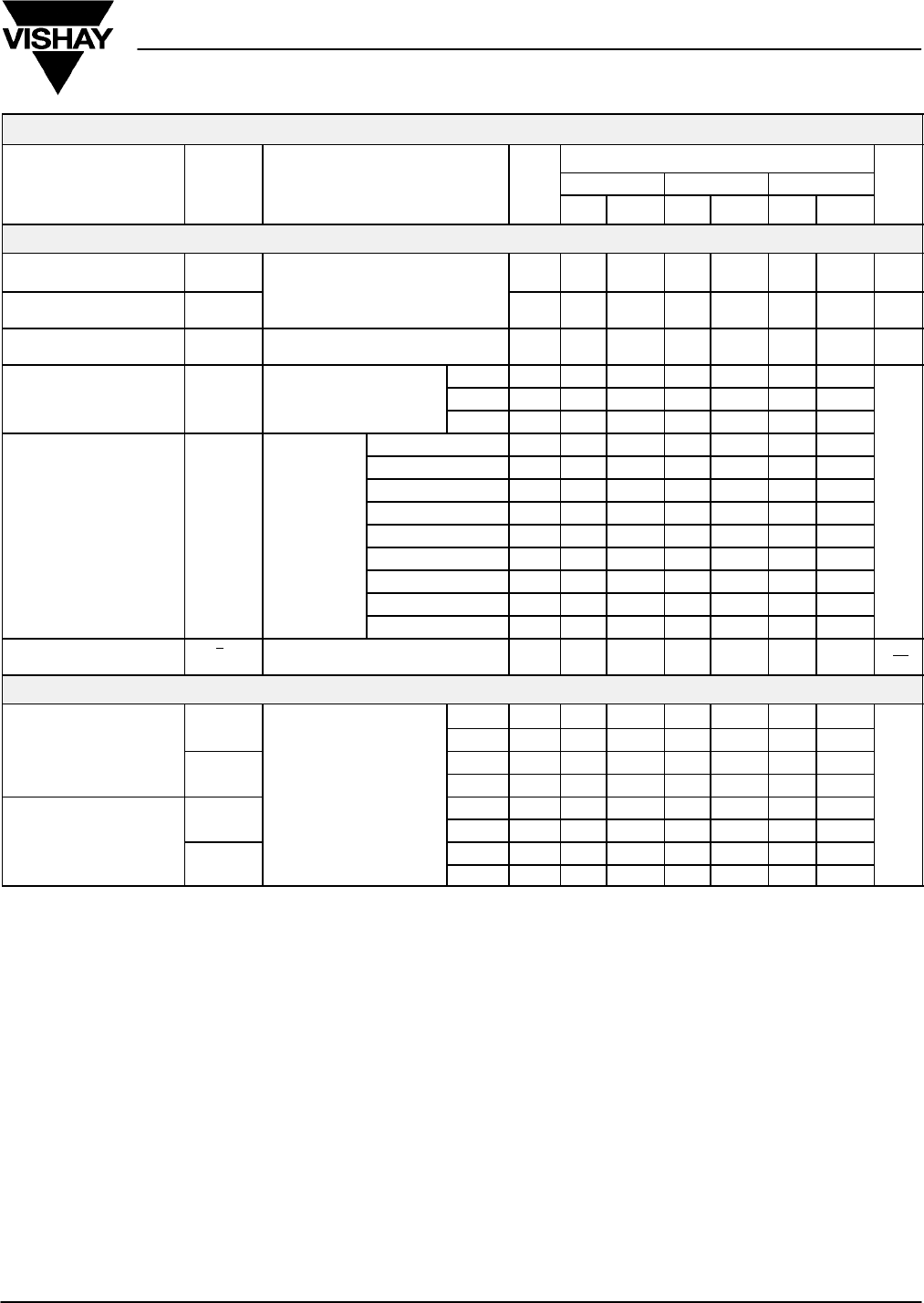
SPECIFICATIONS (TA = 25_C UNLESS OTHERWISE NOTED)
Limits
4391 4392 4393
Parameter Symbol Test Conditions TypaMin Max Min Max Min Max Unit
Dynamic
Common-Source
Forward Transconductance gfs 6 mS
Common-Source
Output Conductance gos
VDS = 20 V, ID = 1 mA, f = 1 kHz
25 S
Drain-Source
On-Resistance rDS(on) VGS = 0 V, ID = 0 mA , f = 1 kHz 30 60 100
2N 12 14 14 14
Common-Source
Input Capacitance Ciss VDS = 20 V, VGS = 0 V
f = 1 MHz PN 12 16 16 16
Input Capacitance iss f = 1 MHz SST 13
2N: VGS = –5 V 3.3 3.5
2N: VGS = –7 V 3.2 3.5
2N: VGS = –12 V 2.8 3.5
PN: VGS = –5 V 3.5 5 pF
Common-Source
Reverse Transfer Crss VDS = 0 V
f = 1 MHz PN: VGS = –7 V 3.4 5
Capacitance rss f = 1 MHz PN: VGS = –12 V 3.0 5
SST: VGS = –5 V 3.6
SST: VGS = –7 V 3.5
SST: VGS = –12 V 3.1
Equivalent Input
Noise Voltage enVDS = 10 V, ID = 10 mA
f = 1 kHz 3nV⁄
√Hz
Switching
2N/PN 2 15 15 15
td(on) SST 2
Turn-On Time 2N/PN 2 5 5 5
trVDD = 10 V SST 2
VGS(H) = 0 V
See Switching Circuit 2N/PN 6 20 35 50 ns
td(off) See Switching Circuit
SST 6
Turn-Off Time 2N/PN 13 15 20 30
tfSST 13
Notes
a. Typical values are for DESIGN AID ONLY, not guaranteed nor subject to production testing. NCB
b. Pulse test: PW v300 s duty cycle v3%.
2N/PN/SST4391 Series
Vishay Siliconix
www.vishay.com
7-4 Document Number: 70241
S-04028—Rev. F, 04-Jan-01
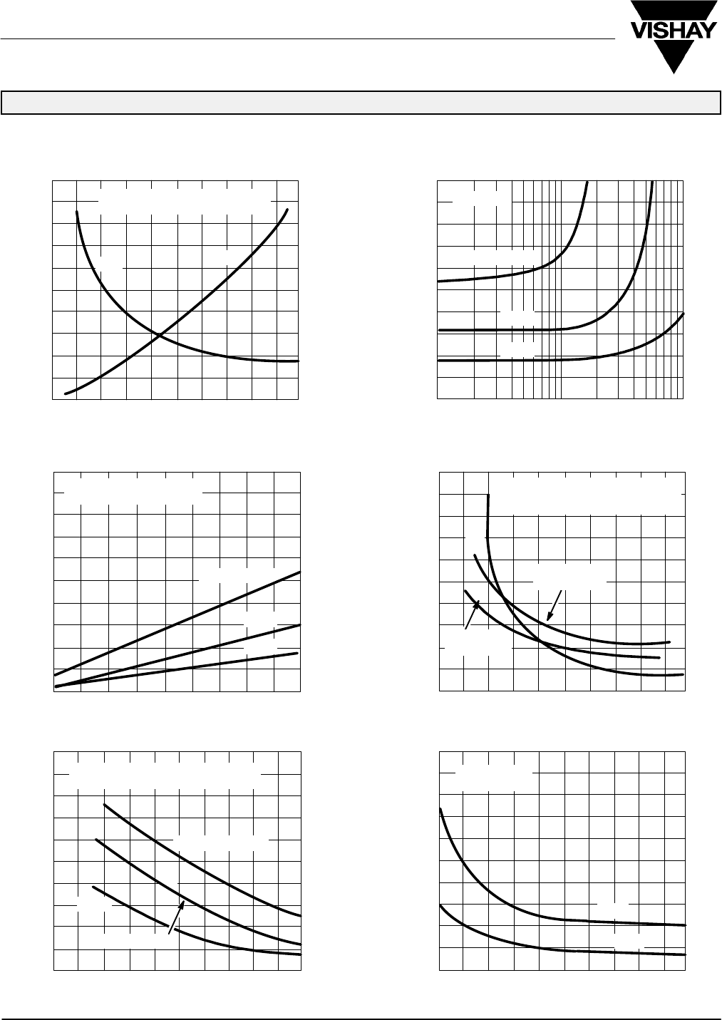
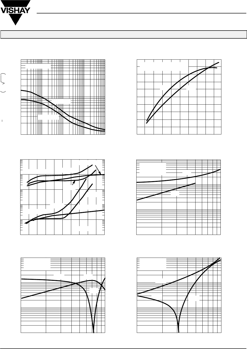
TYPICAL CHARACTERISTICS (TA = 25_C UNLESS OTHERWISE NOTED)
160
120
On-Resistance and Drain Current
vs. Gate-Source Cutoff Voltage On-Resistance vs. Drain Current
100
0–10
0
200
160
0
rDS IDSS
rDS @ ID = 1 mA, VGS = 0 V
IDSS @ VDS = 20 V, VGS = 0 V
100
0
1 10 100
On-Resistance vs. Temperature
200
–55 25 125
0–15 85
ID = 1 mA
rDS changes X 0.7%/_C
Turn-On Switching
5
0–10
4
3
2
1
0
Switching Time (ns)
td(on) @
ID = 3 mA
td(on) @
ID = 12 mA
tr approximately independent of ID
VDD = 5 V, RG = 50 W
VGS(L) = –10 V
Turn-Off Switching
30
010
24
18
12
6
0
VGS(off) = –2 V
VGS(off) = –8 V
td(off) independent of device VGS(off)
VDD = 5 V, VGS(L) = –10 V
Capacitance vs. Gate-Source Voltage
30
–20
24
18
12
6
0
Capacitance (pF)
f = 1 MHz
VDS = 0 V
0
VGS(off) – Gate-Source Cutoff Voltage (V)
TA – Temperature (_C)
VGS – Gate-Source Voltage (V)
VGS(off) – Gate-Source Cutoff Voltage (V)
ID – Drain Current (mA)
ID – Drain Current (mA)
80
60
40
20
80
40
80
60
40
20
–2–4–6–8
–35
120
80
40
5 45 65 105 –2–4–6–8
24 68 –4–8–12 –16
Switching Time (ns)
VGS(off) = –2 V
–4 V
–8 V
TA = 25_C
tr
VGS(off) = –2 V
–4 V
–8 V
td(off) Ciss
Crss
tf
rDS(on) – Drain-Source On-Resistance ( Ω )
rDS(on) – Drain-Source On-Resistance ( Ω )
rDS(on) – Drain-Source On-Resistance ( Ω )
IDSS – Saturation Drain Current (mA)
2N/PN/SST4391 Series
Vishay Siliconix
Document Number: 70241
S-04028—Rev. F, 04-Jan-01 www.vishay.com
7-5
TYPICAL CHARACTERISTICS (TA = 25_C UNLESS OTHERWISE NOTED)
Noise Voltage vs. Frequency
100
10
110 100 1 k 100 k10 k
VDS = 10 V
Forward Transconductance and Output onductance
vs. Gate-Source Cutoff Voltage*
50
0
0–2–10
500
200
0
gfs and gos @ VDS = 20 V
VGS = 0 V, f = 1 kHz
Gate Leakage Current
030
TA = 125_C
TA = 25_C
Common-Gate Input Admittance
100
10
1
0.1 100 1000200 500
(mS)
VDG = 10 V
ID = 10 mA
TA = 25_C
Common-Gate Forward Admittance Common-Gate Reverse Admittance
100
10
1
0.1100 1000200 500
(mS)
VDG = 10 V
ID = 10 mA
TA = 25_C
10
1.0
0.1
0.01
100 1000200 500
VDG = 10 V
ID = 10 mA
TA = 25_C
(mS)
VDG – Drain-Gate Voltage (V)
VGS(off) – Gate-Source Cutoff Voltage (V)f – Frequency (Hz)
f – Frequency (MHz)
f – Frequency (MHz) f – Frequency (MHz)
40
30
20
10
–4–6–8
IGSS @ 125_C
6 121824
400
200
100
0.1 pA
1 pA
10 pA
100 pA
1 nA
10 nA
ID = 1 mA
ID = 10 mA
gfs gos
1 mA
IGSS @ 25_C
ID = 10 mA gig
big
–gfg bfg
gfg
–grg
–brg
+grg
10 mA
IG(on) @ ID
1 mA
en – Noise Voltage nV / Hz
gos – Output Conductance (µS)
gfs – Forward Transconductance (mS)
IG – Gate Leakage)
51 Ω
51 Ω
1 kΩ
VIN
Scope
VDD
RL
OUT
VGS(H)
VGS(L)
2N/PN/SST4391 Series
Vishay Siliconix
www.vishay.com
7-6 Document Number: 70241
S-04028—Rev. F, 04-Jan-01
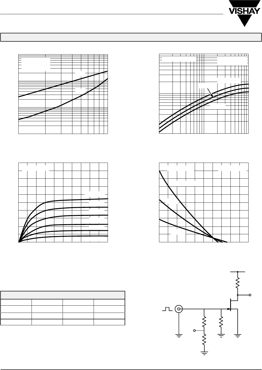
TYPICAL CHARACTERISTICS (TA = 25_C UNLESS OTHERWISE NOTED)
Common-Gate Output Admittance
100
10
1
0.1
100 1000200 500
(mS)
VDG = 10 V
ID = 10 mA
TA = 25_C
f – Frequency (MHz)
Transfer Characteristics
100
0–5
80
60
40
20
0
VGS – Gate-Source Voltage (V)
–1–2–3–4
VDS = 20 V
TA = –55_C
25_C
Transconductance vs. Drain Current
100
10
1
0.1 1.0 10
ID – Drain Current (mA)
VGS(off) = –2 V
Output Characteristics
100
010
80
60
40
20
0
VDS – Drain-Source Voltage (V)
2468
125_C
gog
bog
TA = –55_C
125_C
VGS = 0 V
–0.5 V
–1.0 V
–1.5 V
–2.0 V
–2.5 V
VGS(off) = –4 V
25_C
VDS = 10 V
f = 1 kHz
VGS(off) = –4 V
gfs – Forward Transconductance (mS)
ID – Drain Current (mA)
ID – Drain Current (mA)
SWITCHING TIME TEST CIRCUIT
4391 4392 4393
VGS(L) –12 V –7 V –5 V
RL*800 1600 3000
ID(on) 12 mA 6 mA 3 mA
*Non-inductive
INPUT PULSE SAMPLING SCOPE
Rise Time < 1 ns
Fall Time < 1 ns
Pulse Width 100 ns
PRF 1 MHz
Rise Time 0.4 ns
Input Resistance 10 M
Input Capacitance 1.5 pF
See Typical Characteristics curves for changes.
