2N5484, 2N5485, 2N5486, SST5484, SST5485, SST5486 Datasheet. Www.s Manuals.com. Vishay
User Manual: Marking of electronic components, SMD Codes H4, H4*, H4**, H4033, H40B**, H40D**, H414, H41B**, H41D**, H41E**, H42B**, H42D**. Datasheets BCW69R, BZX585-C8V2, EMH4, HM4033, HMC414MS8G, IMH4A, MMSZ5244, PZU3.6B2, R1162D181B5, R1162D181D5, R1162D281B5, R1162D281D5, R1162D281E5, R1162D401B, R1162D401D, RT9013-30GQW, SST5484, TC1189-QECT, UMH4N.
Open the PDF directly: View PDF ![]() .
.
Page Count: 8
2N/SST5484 Series
Vishay Siliconix
Document Number: 70246
S-50148—Rev. G, 24-Jan-05
www.vishay.com
1
N-Channel JFETs
2N5484 SST5484
2N5485 SST5485
2N5486 SST5486
PRODUCT SUMMARY
Part Number VGS(off) (V) V(BR)GSS Min (V) gfs Min (mS) IDSS Min (mA)
2N/SST5484 −0.3 to −3−25 3 1
2N/SST5485 −0.5 to −4−25 3.5 4
2N/SST5486 −2 to −6−25 4 8
FEATURES BENEFITS APPLICATIONS
DExcellent High-Frequency Gain:
Gps 13 dB (typ) @ 400 MHz − 5485/6
DVery Low Noise: 2.5 dB (typ) @
400 MHz − 5485/6
DVery Low Distortion
DHigh AC/DC Switch Off-Isolation
DWideband High Gain
DVery High System Sensitivity
DHigh Quality of Amplification
DHigh-Speed Switching Capability
DHigh Low-Level Signal Amplification
DHigh-Frequency Amplifier/Mixer
DOscillator
DSample-and-Hold
DVery Low Capacitance Switches
DESCRIPTION
The 2N/SST5484 series consists of n-channel JFETs
designed to provide high-performance amplification,
especially at high frequencies up to and beyond 400 MHz.
The 2N series, TO-226AA (TO-92), and SST series, TO-236
(SOT-23), packages provide low-cost options and are
available with tape-and-reel to support automated assembly
(see Packaging Information).
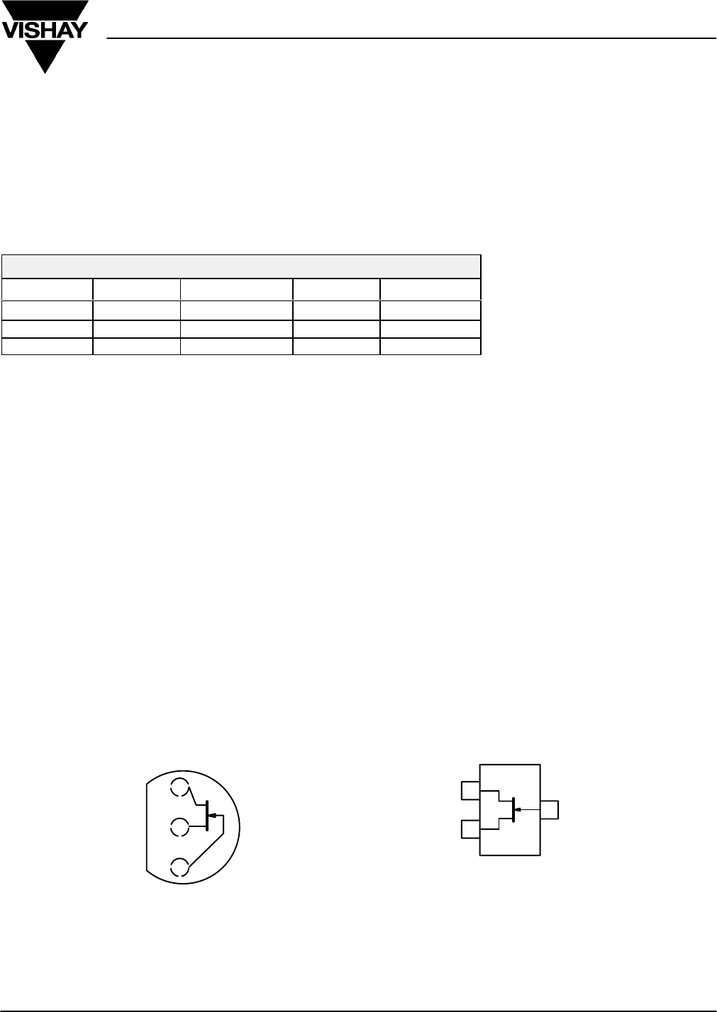
D
S
G
TO-236
(SOT-23
)
2
3
1
Top View
SST5484 (H4)*
SST5485 (H5)*
SST5486 (H6)*
*Marking Code for TO-236
D
S
G
TO-226AA
(TO-92)
Top View
2N5484
2N5485
2N5486
1
2
3
For applications information see AN102 and AN105.
2N/SST5484 Series
Vishay Siliconix
www.vishay.com
2
Document Number: 70246
S-50148—Rev. G, 24-Jan-05
ABSOLUTE MAXIMUM RATINGS
Gate-Drain, Gate-Source Voltage −25 V. . . . . . . . . . . . . . . . . . . . . . . . . . . . . . .
Gate Current 10 mA. . . . . . . . . . . . . . . . . . . . . . . . . . . . . . . . . . . . . . . . . . . . . . . . .
Lead Temperature 300_C. . . . . . . . . . . . . . . . . . . . . . . . . . . . . . . . . . . . . . . . . . . .
Storage Temperature −65 to 150_C. . . . . . . . . . . . . . . . . . . . . . . . . . . . . . . . . . .
Operating Junction Temperature −55 to 150_C. . . . . . . . . . . . . . . . . . . . . . . . . .
Power Dissipationa350 mW. . . . . . . . . . . . . . . . . . . . . . . . . . . . . . . . . . . . . . . . .
Notes
a. Derate 2.8 mW/_C above 25_C
SPECIFICATIONS FOR 2N SERIES (TA = 25_C UNLESS OTHERWISE NOTED)
Limits
2N5484 2N5485 2N5486
Parameter Symbol Test Conditions TypaMin Max Min Max Min Max Unit
Static
Gate-Source
Breakdown Voltage V(BR)GSS IG = −1 A , VDS = 0 V −35 −25 −25 −25
V
Gate-Source Cutoff Voltage VGS(off) VDS = 15 V, ID = 10 nA −0.3 −3−0.5 −4−2−6
V
Saturation Drain CurrentbIDSS VDS = 15 V, VGS = 0 V 1 5 4 10 8 20 mA
Gate Reverse Current
IGSS
VGS = −20 V, VDS = 0 V −0.002 −1−1−1
nA
Gate Reverse Current IGSS TA = 100_C−0.2 −200 −200 −200 nA
Gate Operating CurrentcIGVDG = 10 V, ID = 1 mA −20 pA
Gate-Source
Forward VoltagecVGS(F) IG = 10 mA , VDS = 0 V 0.8 V
Dynamic
Common-Source
Forward TransconductanceNO TAG gfs VDS = 15 V, VGS = 0 V
3 6 3.5 7 4 8 mS
Common-Source
Output ConductanceNO TAG gos
VDS = 15 V
,
VGS = 0 V
f = 1 kHz 50 60 75 S
Common-Source
Input Capacitance Ciss 2.2 5 5 5
Common-Source
Reverse Transfer Capacitance Crss VDS = 15 V, VGS = 0 V
f = 1 MHz 0.7 1 1 1 pF
Common-Source
Output Capacitance Coss 1 2 2 2
Equivalent Input
Noise VoltagecenVDS = 15 V, VGS = 0 V
f = 100 Hz 10 nV⁄
√Hz
High-Frequency
Common-Source
d
Yf(RE)
f = 100 MHz 5.5 2.5
mS
Common-Source
TransconductancedYfs(RE) f = 400 MHz 5.5 3 3.5 mS
Common-Source
d
Y(RE)
VDS = 15 V f = 100 MHz 45 75
S
Common-Source
Output ConductancedYos(RE)
VDS = 15 V
VGS = 0 V f = 400 MHz 65 100 100 S
Common-Source
d
Yi(RE)
f = 100 MHz 0.05 0.1
mS
Common-Source
Input ConductancedYis(RE) f = 400 MHz 0.8 1 1 mS
CS P Gi
d
G
VDS = 15 V, ID = 1 mA
f = 100 MHz 20 16 25
Common-Source Power GaindGps VDS = 15 V f = 100 MHz 21 18 30 18 30
VDS = 15 V
ID = 4 mA f = 400 MHz 13 10 20 10 20
VDS = 15 V, VGS = 0 V
RG = 1 M , f = 1 kHz 0.3 2.5 2.5 2.5 dB
Noise FiguredNF
VDS = 15 V, ID = 1 mA
RG = 1 k , f = 100 MHz 2 3
g
VDS = 15 V
ID = 4 mA
f = 100 MHz 1 2 2
I
D
=
4
m
A
RG = 1 kf = 400 MHz 2.5 4 4
2N/SST5484 Series
Vishay Siliconix
Document Number: 70246
S-50148—Rev. G, 24-Jan-05
www.vishay.com
3
SPECIFICATIONS FOR SST SERIES (TA = 25_C UNLESS OTHERWISE NOTED)
Limits
SST5484 SST5485 SST5486
Parameter Symbol Test Conditions TypbMin Max Min Max Min Max Unit
Static
Gate-Source
Breakdown Voltage V(BR)GSS IG = −1 A , VDS = 0 V −35 −25 −25 −25
V
Gate-Source Cutoff Voltage VGS(off) VDS = 15 V, ID = 10 nA −0.3 −3−0.5 −4−2−6
V
Saturation Drain CurrentbIDSS VDS = 15 V, VGS = 0 V 1 5 410 8 20 mA
Gate Reverse Current
IGSS
VGS = −20 V, VDS = 0 V −0.002 −1−1−1
nA
Gate Reverse Current IGSS TA = 100_C−0.2 −200 −200 −200 nA
Gate Operating CurrentcIGVDG = 10 V, ID = 1 mA −20 pA
Gate-Source
Forward VoltagecVGS(F) IG = 10 mA , VDS = 0 V 0.8 V
Dynamic
Common-Source
Forward TransconductanceNO TAG gfs VDS = 15 V, VGS = 0 V
3 6 3.5 7 4 8 mS
Common-Source
Output ConductanceNO TAG gos
VDS = 15 V
,
VGS = 0 V
f = 1 kHz 50 60 75 S
Common-Source
Input Capacitance Ciss 2.2
Common-Source
Reverse Transfer
Capacitance
Crss VDS = 15 V, VGS = 0 V
f = 1 MHz 0.7 pF
Common-Source
Output Capacitance Coss 1
Equivalent Input
Noise VoltagecenVDS = 15 V, VGS = 0 V
f = 100 Hz 10 nV⁄
√Hz
High-Frequency
Common-Source
Yf
f = 100 MHz 5.5
mS
Common-Source
Transconductance Yfs f = 400 MHz 5.5 mS
Common-Source
Y
VDS = 15 V f = 100 MHz 45
S
Common-Source
Output Conductance Yos
VDS = 15 V
VGS = 0 V f = 400 MHz 65 S
Common-Source
Yi
f = 100 MHz 0.05
mS
Common-Source
Input Conductance Yis f = 400 MHz 0.8 mS
Common
-
Source
G
VDS = 15 V, ID = 1 mA
f = 100 MHz 20
Common
-
So
u
rce
Power Gain Gps VDS = 15 V f = 100 MHz 21
VDS = 15 V
ID = 4 mA f = 400 MHz 13
VDS = 15 V, VGS = 0 V
RG = 1 M , f = 1 kHz 0.3 dB
Noise Figure NF
VDS = 15 V, ID = 1 mA
RG = 1 k , f = 100 MHz 2
g
VDS = 15 V
ID = 4 mA
f = 100 MHz 1
ID = 4 mA
RG = 1 kf = 400 MHz 2.5
Notes
a. Typical values are for DESIGN AID ONLY, not guaranteed nor subject to production testing. NH
b. Pulse test: PW v300 s duty cycle v3%.
c. This parameter not registered with JEDEC.
d. Not a production test.
Stresses beyond those listed under “Absolute Maximum Ratings” may cause permanent damage to the device. These are stress ratings only, and functional operation
of the device at these or any other conditions beyond those indicated in the operational sections of the specifications is not implied. Exposure to absolute maximum
rating conditions for extended periods may affect device reliability.
2N/SST5484 Series
Vishay Siliconix
www.vishay.com
4
Document Number: 70246
S-50148—Rev. G, 24-Jan-05
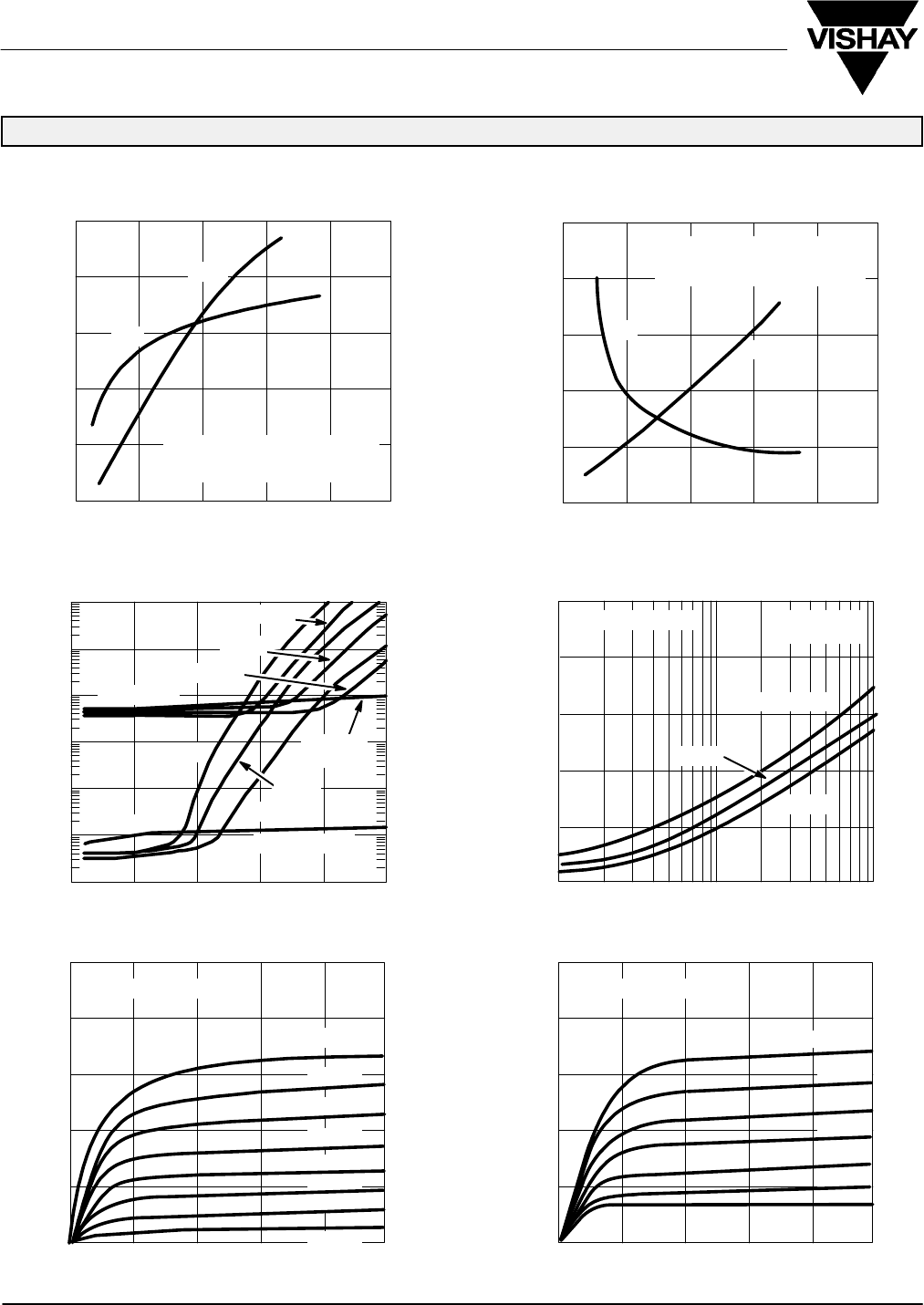
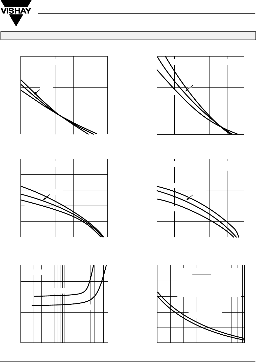
TYPICAL CHARACTERISTICS (TA = 25_C UNLESS OTHERWISE NOTED)
On-Resistance and Output Conductance
vs. Gate-Source Cutoff Voltage
rDS
gos
rDS @ ID = 300 A, VGS = 0 V
gos @ VDS = 10 V, VGS = 0 V
f = 1 kHz
Drain Current and Transconductance
vs. Gate-Source Cutoff Voltage
IDSS
gfs
IDSS @ VDS = 10 V, VGS = 0 V
gfs @ VDS = 10 V, VGS = 0 V
f = 1 kHz
VGS(off) − Gate-Source Cutoff Voltage (V)
VDG − Drain-Gate Voltage (V) ID − Drain Current (mA)
VDS − Drain-Source Voltage (V) VDS − Drain-Source Voltage (V)
Gate Leakage Current
0.1 mA
IGSS @ 25_C
TA = 25_C
TA = 125_C
IGSS @
125_C
Output Characteristics Output Characteristics
Common-Source Forward
Transconductance vs. Drain Current
0.1 1 10
10
8
0
VGS(off) = −3 V
TA = −55_C
25_C
125_C
−0.2 V
−0.4 V
−0.6 V
−0.8 V
−1.2 V
−1.0 V
VGS = 0 V
−0.6 V
−0.9 V
−1.2 V
−1.5 V
−1.8 V
VGS = 0 V
−0.3 V
10
8
0
6
4
2
20
0
16
12
8
4
0−10−2−4−6−8
100
80
0
60
40
20
500
0
400
300
200
100
0−10−2−4−6−8
012841620
0.1 pA
1 pA
10 pA
100 pA
1 nA
10 nA
100 nA
6
4
2
10
0
8
6
4
2
01024 68
15
0
12
9
6
3
01024 68
VGS(off) − Gate-Source Cutoff Voltage (V)
VDS = 10 V
f = 1 kHz
VGS(off) = −2 V VGS(off) = −3 V
ID = 5 mA
1 mA
0.1 mA
ID = 5 mA
1 mA
−1.4 V
gos − Output Conductance (µS)
rDS(on) − Drain-Source On-Resistance ( Ω )
gfs − Forward Transconductance (mS)
IDSS − Saturation Drain Current (mA)
gfs − Forward Transconductance (mS)
IG − Gate LeakageID − Drain Current (mA)
ID − Drain Current (mA)
2N/SST5484 Series
Vishay Siliconix
Document Number: 70246
S-50148—Rev. G, 24-Jan-05
www.vishay.com
5
TYPICAL CHARACTERISTICS (TA = 25_C UNLESS OTHERWISE NOTED)
VGS − Gate-Source Voltage (V) VGS − Gate-Source Voltage (V)
Transfer Characteristics
VGS(off) = −2 V
TA = −55_C
125_C
Transfer Characteristics
TA = −55_C
125_C
VGS(off) = −3 V
25_C
VGS − Gate-Source Voltage (V)
Transconductance vs. Gate-Source Voltage
VGS(off) = −2 V
TA = −55_C
125_C
25_C
VGS − Gate-Source Voltage (V)
Transconductance vs. Gate-Source Voltage
TA = −55_C
125_C
25_C
VGS(off) = −3 V
ID − Drain Current (mA) ID − Drain Current (mA)
On-Resistance vs. Drain Current Circuit Voltage Gain vs. Drain Current
0.1 1 10
TA = 25_C
−3 V
VGS(off) = −2 V
100.1
AV+
gfs RL
1)RLgos
Assume VDD = 15 V, VDS = 5 V
RL+
10 V
ID
VGS(off) = −2 V
−3 V
10
0
8
6
4
2
0−2−0.4 −0.8 −1.2 −1.6
300
0
240
180
120
60
10
0
8
6
4
2
0−3−0.6 −1.2 −1.8 −2.4
10
0
8
6
4
2
0−2−0.4 −0.8 −1.2 −1.6
10
0
8
6
4
2
0−3−0.6 −1.2 −1.8 −2.4
100
0
80
60
40
20
VDS = 10 V VDS = 10 V
VDS = 10 V
f = 1 kHz
VDS = 10 V
f = 1 kHz
1
25_C
rDS(on) − Drain-Source On-Resistance ( Ω ) gfs − Forward Transconductance (mS)
gfs − Forward Transconductance (mS)
ID − Drain Current (mA)
ID − Drain Current (mA)
AV − Voltage Gain
2N/SST5484 Series
Vishay Siliconix
www.vishay.com
6
Document Number: 70246
S-50148—Rev. G, 24-Jan-05
TYPICAL CHARACTERISTICS (TA = 25_C UNLESS OTHERWISE NOTED)
Common-Source Input Capacitance
vs. Gate-Source Voltage Common-Source Reverse Feedback
Capacitance vs. Gate-Source Voltage
f = 1 MHz
VDS = 0 V
10 V
VDS = 0 V
10 V
VGS − Gate-Source Voltage (V) VGS − Gate-Source Voltage (V)
f = 1 MHz
Reverse Admittance Output Admittance
Input Admittance Forward Admittance
100
10
1
0.1
100 1000
bis
gis
TA = 25_C
VDS = 15 V
VGS = 0 V
Common Source
(mS)
100
10
1
0.1
100 1000
TA = 25_C
VDS = 15 V
VGS = 0 V
Common Source
(mS)
−bfs
gfs
10
1
0.1
0.01
100 1000
(mS)
TA = 25_C
VDS = 15 V
VGS = 0 V
Common Source −brs
−grs
10
1
0.1
0.01
100 1000
TA = 25_C
VDS = 15 V
VGS = 0 V
Common Source
bos
gos
(mS)
f − Frequency (MHz) f − Frequency (MHz)
f − Frequency (MHz)f − Frequency (MHz)
5
0
4
3
2
1
0−20−4−8−12 −16
3
0
2.4
1.8
1.2
0.6
0−20−4−8−12 −16
200 500 200 500
200 500 200 500
Ciss − Input Capacitance (pF)
Crss − Reverse Feedback Capacitance (pF)
2N/SST5484 Series
Vishay Siliconix
Document Number: 70246
S-50148—Rev. G, 24-Jan-05
www.vishay.com
7
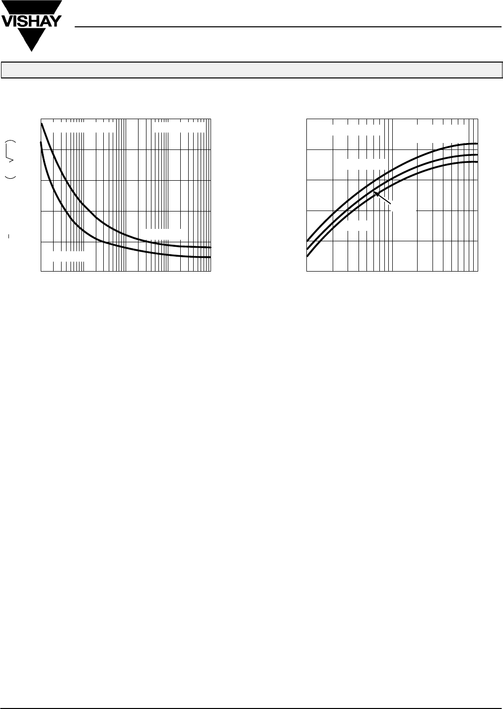
TYPICAL CHARACTERISTICS (TA = 25_C UNLESS OTHERWISE NOTED)
20
0
16
12
8
4
Equivalent Input Noise Voltage vs. Frequency Output Conductance vs. Drain Current
10 100 k10 k
ID = 5 mA
VDS = 10 V
0.1 1 10
TA = −55_C
125_C
VGS(off) = −3 V
ID − Drain Current (mA)f − Frequency (Hz)
20
0
16
12
8
4
ID = IDSS
VDS = 10 V
f = 1 kHz
100 1 k
VGS(off) = −3 V
25_C
en − Noise Voltage nV / Hz
gos − Output Conductance (µS)
Vishay Siliconix maintains worldwide manufacturing capability. Products may be manufactured at one of several qualified locations. Reliability data for Silicon Technology and
Package Reliability represent a composite of all qualified locations. For related documents such as package/tape drawings, part marking, and reliability data, see
http://www.vishay.com/ppg?70246.