2N7000, 2N7002, BS170, VQ1000J, VQ1000P Datasheet. Www.s Manuals.com. 2n7000 2n7002 Bs170 Vq1000j Vishay
User Manual: Marking of electronic components, SMD Codes 72, 72*, 72***, 720, 7200, 7201A, 7212, 7217-33, 722, 723, 72N025S, 72W. Datasheets 2N7002, 2N7002T, 2N7002TB, 2N7002W, AON7200, AP7217-33SG-13, APW7212QB, BSC072N025S G, EUP7201-1.8/2.8JIR1, FMMT720, FMMT722, FMMT723, RT8237DZQW, UDZS3.9B.
Open the PDF directly: View PDF ![]() .
.
Page Count: 7
2N7000/2N7002, VQ1000J/P, BS170
Vishay Siliconix
Document Number: 70226
S-04279—Rev. F, 16-Jul-01 www.vishay.com
11-1
N-Channel 60-V (D-S) MOSFET
PRODUCT SUMMARY
Part Number V(BR)DSS Min (V) rDS(on) Max (W)VGS(th) (V) ID (A)
2N7000 5 @ VGS = 10 V 0.8 to 3 0.2
2N7002 7.5 @ VGS = 10 V 1 to 2.5 0.115
VQ1000J 60 5.5 @ VGS = 10 V 0.8 to 2.5 0.225
VQ1000P 5.5 @ VGS = 10 V 0.8 to 2.5 0.225
BS170 5 @ VGS = 10 V 0.8 to 3 0.5
FEATURES BENEFITS APPLICATIONS
DLow On-Resistance: 2.5 W
DLow Threshold: 2.1 V
DLow Input Capacitance: 22 pF
DFast Switching Speed: 7 ns
DLow Input and Output Leakage
DLow Offset Voltage
DLow-Voltage Operation
DEasily Driven Without Buffer
DHigh-Speed Circuits
DLow Error Voltage
DDirect Logic-Level Interface: TTL/CMOS
DDrivers: Relays, Solenoids, Lamps, Hammers,
Displays, Memories, Transistors, etc.
DBattery Operated Systems
DSolid-State Relays
TO-226AA
(TO-92)
Top View
S
D
G
1
2
3
G
TO-236
(SOT-23)
S
D
Top View
2
3
1
Plastic: VQ1000J
Sidebraze: VQ1000P
Top View
TO-92-18RM
(TO-18 Lead Form)
D
S
G
1
2
3
2N7000
BS170
1
2
3
4
5
6
7
14
13
12
11
10
9
8
Top View
Dual-In-Line
D1D4
S1S4
G1G4
NC NC
G2G3
S2S3
D2D3
N
N
N
N
Marking Code: 72wll
72 = Part Number Code for 2N7002
w = Week Code
ll = Lot Traceability
2N7000/2N7002, VQ1000J/P, BS170
Vishay Siliconix
www.vishay.com
11-2 Document Number: 70226
S-04279—Rev. F, 16-Jul-01
ABSOLUTE MAXIMUM RATINGS (TA = 25_C UNLESS OTHERWISE NOTED)
Single Total Quad
Parameter Symbol 2N7000 2N7002 VQ1000J VQ1000P VQ1000J/P BS170 Unit
Drain-Source Voltage VDS 60 60 60 60 60
Gate-Source Voltage—Non-Repetitive VGSM "40 "40 "30 "25 V
Gate-Source Voltage—Continuous VGS "20 "20 "20 "20 "20
Continuous Drain Current TA= 25_C0.2 0.115 0.225 0.225 0.5
Continuous Drain Current
(TJ = 150_C) TA= 100_CID0.13 0.073 0.14 0.14 0.175 A
Pulsed Drain CurrentaIDM 0.5 0.8 1 1
TA= 25_C0.4 0.2 1.3 1.3 2 0.83
Power Dissipation TA= 100_CPD0.16 0.08 0.52 0.52 0.8 W
Thermal Resistance, Junction-to-Ambient RthJA 312.5 625 96 96 62.5 156 _C/W
Operating Junction and
Storage Temperature Range TJ, Tstg –55 to 150 _C
Notes
a. Pulse width limited by maximum junction temperature.
b. tp v 50 ms.
SPECIFICATIONSĊ2N7000 AND 2N7002 (TA = 25_C UNLESS OTHERWISE NOTED)
Limits
2N7000 2N7002
Parameter Symbol Test Conditions TypaMin Max Min Max Unit
Static
Drain-Source Breakdown Voltage V(BR)DSS VGS = 0 V, ID = 10 mA70 60 60
VDS = VGS, ID = 1 mA 2.1 0.8 3 V
Gate-Threshold Voltage VGS(th) VDS = VGS, ID = 0.25 mA 2.0 1 2.5
VDS = 0 V, VGS = "15 V "10
Gate-Body Leakage IGSS VDS = 0 V, VGS = "20 V "100 nA
VDS = 48 V, VGS = 0 V 1
TC = 125_C1000
m
Zero Gate Voltage Drain Current IDSS VDS = 60 V, VGS = 0 V 1mA
TC = 125_C500
VDS = 10 V, VGS = 4.5 V 0.35 0.075
On-State Drain CurrentbID(on) VDS = 7.5 V, VGS = 10 V 1 0.5 A
VGS = 4.5 V, ID = 0.075 A 4.5 5.3
VGS = 5 V, ID = 0.05 A 3.2 7.5
Drain-Source On-ResistancebrDS(on) TC = 125_C5.8 13.5 W
DS(on)
VGS = 10 V, ID = 0.5 A 2.4 5 7.5
TJ = 125_C4.4 9 13.5
Forward Transconductancebgfs VDS = 10 V, ID = 0.2 A 100 80
Common Source Output Conductancebgos VDS = 5 V, ID = 0.05 A 0.5 mS
Dynamic
Input Capacitance Ciss 22 60 50
Output Capacitance Coss VDS = 25 V, VGS = 0 V
f = 1 MHz 11 25 25 pF
Reverse Transfer Capacitance Crss
f = 1 MHz 2 5 5
2N7000/2N7002, VQ1000J/P, BS170
Vishay Siliconix
Document Number: 70226
S-04279—Rev. F, 16-Jul-01 www.vishay.com
11-3
SPECIFICATIONSĊ2N7000 AND 2N7002 (TA = 25_C UNLESS OTHERWISE NOTED)
Limits
2N7000 2N7002
Parameter Symbol Test Conditions TypaMin Max Min Max Unit
Switchingd
Turn-On Time tON V
DD
= 15 V, R
L
= 25 W7 10
Turn-Off Time tOFF
VDD = 15 V, RL = 25
W
ID ^0.5 A, VGEN = 10 V, RG = 25 W7 10
Turn-On Time tON VDD = 30 V, RL = 150 W7 20 ns
Turn-Off Time tOFF
VDD = 30 V, RL = 150
W
ID ^ 0.2 A, VGEN = 10 V, RG = 25 W11 20
SPECIFICATIONSĊVQ1000J/P AND BS170 (TA = 25_C UNLESS OTHERWISE NOTED)
Limits
VQ1000J/P BS170
Parameter Symbol Test Conditions TypaMin Max Min Max Unit
Static
Drain-Source Breakdown Voltage V(BR)DSS VGS = 0 V, ID = 100 mA70 60 60
Gate-Threshold Voltage VGS(th) VDS = VGS, ID = 1 mA 2.1 0.8 2.5 0.8 3 V
VDS = 0 V, VGS = "10 V "100
Gate-Body Leakage IGSS TJ = 125_C"500 nA
GSS
VDS = 0 V, VGS = "15 V "10
VDS = 25 V, VGS = 0 V 0.5
Zero Gate Voltage Drain Current IDSS VDS = 48 V, VGS = 0 V, TJ = 125_C500 mA
DSS
VDS = 60 V, VGS = 0 V 10
m
On-State Drain CurrentbID(on) VDS = 10 V, VGS = 10 V 1 0.5 A
VGS = 5 V, ID = 0.2 A 4 7.5
VGS = 10 V, ID = 0.2 A 2.3 5
W
Drain-Source On-ResistancebrDS(on) VGS = 10 V, ID = 0.3 A 2.3 5.5 W
TJ = 125_C4.2 7.6
VDS = 10 V, ID = 0.2 A 100
Forward Transconductancebgfs VDS = 10 V, ID = 0.5 A 100 mS
Common Source Output Conductancebgos VDS =5 V, ID = 0.05 A 0.5
Dynamic
Input Capacitance Ciss 22 60 60
Output Capacitance Coss VDS =25 V, VGS = 0 V
f = 1 MHz 11 25 pF
Reverse Transfer Capacitance Crss
f = 1 MHz 2 5
Switchingd
Turn-On Time tON V
DD
= 15 V, R
L
= 23 W7 10
Turn-Off Time tOFF
VDD = 15 V, RL = 23
W
ID ^ 0.6 A, VGEN = 10 V, RG = 25 W7 10
Turn-On Time tON VDD = 25 V, RL = 125 W7 10 ns
Turn-Off Time tOFF
VDD = 25 V, RL = 125
W
ID ^ 0.2 A, VGEN = 10 V, RG = 25 W7 10
Notes
a. For DESIGN AID ONLY, not subject to production testing. VNBF06
b. Pulse test: PW v80 ms duty cycle v1%.
c. This parameter not registered with JEDEC.
d. Switching time is essentially independent of operating temperature.
2N7000/2N7002, VQ1000J/P, BS170
Vishay Siliconix
www.vishay.com
11-4 Document Number: 70226
S-04279—Rev. F, 16-Jul-01
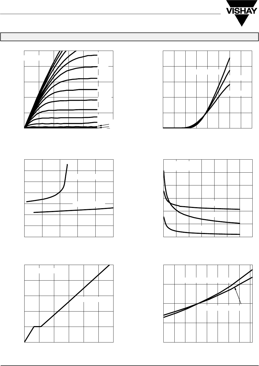
TYPICAL CHARACTERISTICS (TA = 25_C UNLESS OTHERWISE NOTED)
CapacitanceOn-Resistance vs. Drain Current
0.0
0.2
0.4
0.6
0.8
1.0
0123456
0.0
0.2
0.4
0.6
0.8
1.0
012345678
Output Characteristics Transfer Characteristics
VDS – Drain-to-Source Voltage (V)
VGS = 10, 9, 8, 7 V 6.5 V
VGS – Gate-to-Source Voltage (V)
TJ = –55_C
25_C
125_C
6 V
5.5 V
5 V
4.5 V
4 V
3.5 V
3 V 2.5 V
2, 1 V
0
4
8
12
16
20
0 400 800 1200 1600 2000 2400
0.0
0.5
1.0
1.5
2.0
–55 –30 –5 20 45 70 95 120 145
0
1
2
3
4
5
6
7
0.0 0.2 0.4 0.6 0.8 1.0
0
10
20
30
40
50
60
0 5 10 15 20 25 30 35
Gate Charge
Qg – Total Gate Charge (pC)
VDS – Drain-to-Source Voltage (V)
Crss
Coss
Ciss
ID = 0.5 A
ID – Drain Current (A)
On-Resistance vs. Junction Temperature
VGS = 10 V, rDS @ 0.5 A
TJ – Junction Temperature (_C)
rDS @ 10 V = VGS
rDS @ 5 V = VGS
VGS = 5 V, rDS @ 0.05 A
VGS = 0 V
f = 1 MHz
VDS = 30 V
ID – Drain Current (A)
ID – Drain Current (A)
rDS(on) – On-Resistance ( Ω )
C – Capacitance (pF)
VGS – Gate-to-Source Voltage (V)
rDS(on) – On-Resistance ( Ω )
(Normalized)
2N7000/2N7002, VQ1000J/P, BS170
Vishay Siliconix
Document Number: 70226
S-04279—Rev. F, 16-Jul-01 www.vishay.com
11-5
TYPICAL CHARACTERISTICS (TA = 25_C UNLESS OTHERWISE NOTED)
0
1
2
3
4
5
6
0 2 4 6 8 101214161820
0.001
0.010
0.100
1.000
0.0 0.2 0.4 0.6 0.8 1.0 1.2 1.4
Source-Drain Diode Forward Voltage On-Resistance vs. Gate-to-Source Voltage
VSD – Source-to-Drain Voltage (V) VGS – Gate-to-Source Voltage (V)
500 mA
ID = 50 mA
TJ = 25_C
TJ = 125_C
Threshold Voltage
–0.75
–0.50
–0.25
–0.00
0.25
0.50
–50 –25 0 25 50 75 100 125 150
ID = 250 mA
10 K
Duty Cycle = 0.5
0.2
0.1
0.05
0.02
Single Pulse
1
0.01
0.1
0.01
0.1 1 10010 1 K
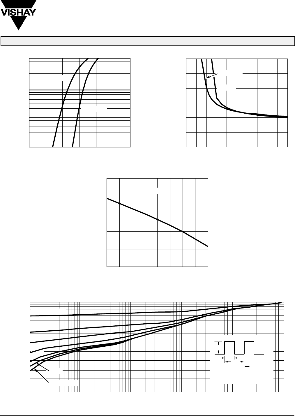
Normalized Effective Transient Thermal Impedance, Junction-to-Ambient (TO-226AA, BS170 Only)
Normalized Effective Transient
Thermal Impedance
t1 – Square Wave Pulse Duration (sec)
1. Duty Cycle, D =
2. Per Unit Base = RthJA = 156_C/W
3. TJM – TA = PDMZthJA(t)
t1
t2
t1
Notes:
PDM
t2
IS – Source Current (A)
rDS(on) – On-Resistance ( Ω )
VGS(th) – Variance (V)

Document Number: 91000 www.vishay.com
Revision: 18-Jul-08 1
Disclaimer
Legal Disclaimer Notice
Vishay
All product specifications and data are subject to change without notice.
Vishay Intertechnology, Inc., its affiliates, agents, and employees, and all persons acting on its or their behalf
(collectively, “Vishay”), disclaim any and all liability for any errors, inaccuracies or incompleteness contained herein
or in any other disclosure relating to any product.
Vishay disclaims any and all liability arising out of the use or application of any product described herein or of any
information provided herein to the maximum extent permitted by law. The product specifications do not expand or
otherwise modify Vishay’s terms and conditions of purchase, including but not limited to the warranty expressed
therein, which apply to these products.
No license, express or implied, by estoppel or otherwise, to any intellectual property rights is granted by this
document or by any conduct of Vishay.
The products shown herein are not designed for use in medical, life-saving, or life-sustaining applications unless
otherwise expressly indicated. Customers using or selling Vishay products not expressly indicated for use in such
applications do so entirely at their own risk and agree to fully indemnify Vishay for any damages arising or resulting
from such use or sale. Please contact authorized Vishay personnel to obtain written terms and conditions regarding
products designed for such applications.
Product names and markings noted herein may be trademarks of their respective owners.