2N7000, 2N7002, NDF7000A, NDS7002A Datasheet. Www.s Manuals.com. 2n7000 2n7002 Ndf7000a National
User Manual: Marking of electronic components, SMD Codes 7002, 7005, 702, 702⚫, 702*, 703 *, 7030L, 704, 705, 709, 709**, 70N10L, 70T. Datasheets 2N7002, 2N7002-G, 2N7002DW, 2N7002E, 2N7002K, 2N7002L, 2N7002MTF, 2V7002K, 2V7002L, FAN7005M, FCX705, G709RCUf, G709T1Uf, L2N7002LT1G, MTN138ZN3, MTN7002N3, MTN7002ZHN3, MTNK1N3, MTNK2N3, PH7030L, SPB70N10L, SPI70N10L, SPP70N10L, TK71570AS.
Open the PDF directly: View PDF ![]() .
.
Page Count: 11
TL/G/11378
2N7000/2N7002/NDF7000A/NDS7002A N-Channel Enhancement Mode Field Effect Transistor
March 1993
2N7000/2N7002/NDF7000A/NDS7002A
N-Channel Enhancement Mode Field Effect Transistor
General Description
These n-channel enhancement mode field effect transistors
are produced using National’s very high cell density third
generation DMOS technology. These products have been
designed to minimize on-state resistance provide rugged
and reliable performance and fast switching. They can be
used, with a minimum of effort, in most applications requir-
ing up to 400 mA DC and can deliver pulsed currents up to
2A. This product is particularly suited to low voltage, low
current applications, such as small servo motor controls,
power MOSFET gate drivers, and other switching applica-
tions.
Features
YEfficient high density cell design approaching
(3 million/in2)
YVoltage controlled small signal switch
YRugged
YHigh saturation current
YLow RDS (ON)
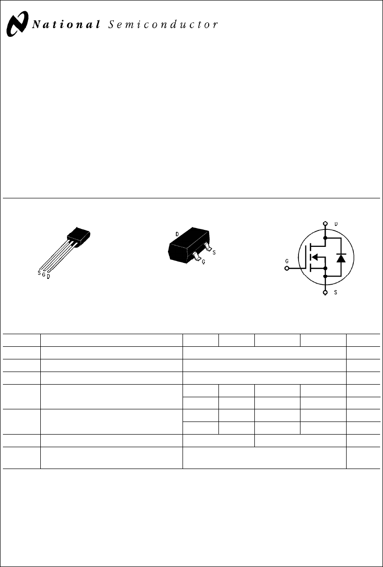
TL/G/11378–1
TO-92
7000 Series
TL/G/11378–2
TO-236 AB
(SOT-23)
7002 Series
TL/G/11378–3
Absolute Maximum Ratings
Symbol Parameter 2N7000 2N7002 NDF7000A NDS7002A Units
VDSS Drain-Source Voltage 60 V
VDGR Drain-Gate Voltage (RGS s1MX)60V
V
GSS Gate-Source Voltage g40 V
IDDrain CurrentÐContinuous 200 115 400 280 mA
ÐPulsed 500 800 2000 1500 mA
PDTotal Power Dissipation @TAe25§C 400 200 625 300 mW
Derating above 25§C 3.2 1.6 5 2.4 mW/§C
TJ,T
STG Operating and Storage Temperature Range b55 to 150 b65 to 150 §C
TLMaximum Lead Temperature for Soldering 300 §C
Purposes, (/16*from Case for 10 Seconds
C1995 National Semiconductor Corporation RRD-B30M115/Printed in U. S. A.
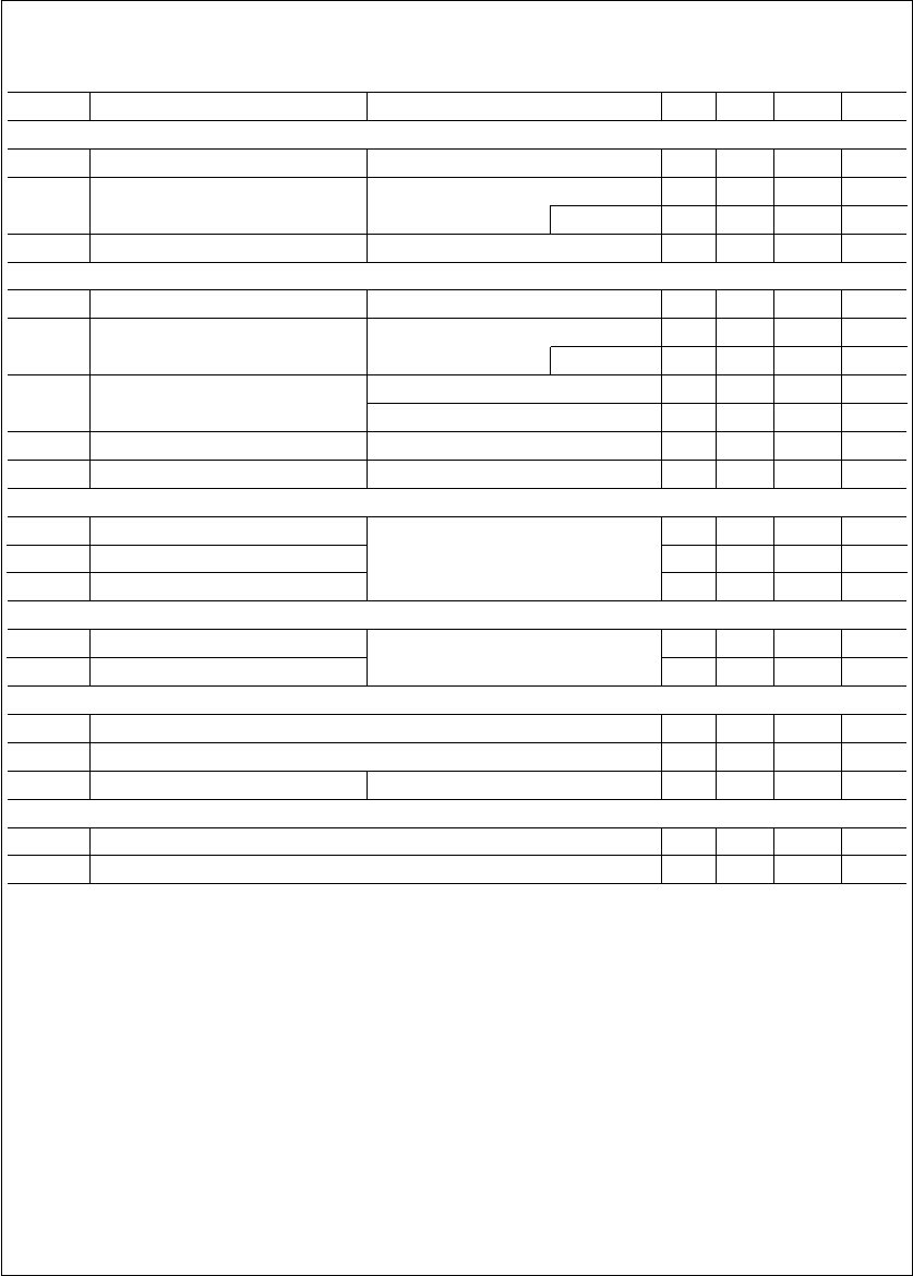
2N7000
Electrical Characteristics TCe25§C unless otherwise noted
Symbol Parameter Conditions Min Typ Max Units
OFF CHARACTERISTICS
BVDSS Drain-Source Breakdown Voltage VGS e0V, IDe10 mA60 V
I
DSS Zero Gate Voltage Drain Current VDS e48V, VGS e0V 1 mA
TCe125§C1mA
I
GSSF Gate-Body Leakage, Forward VGS eb
15V, VDS e0V b10 nA
ON CHARACTERISTICS*
VGS(th) Gate Threshold Voltage VDS eVGS,I
De1 mA 0.8 2.1 3 V
rDS(ON) Static Drain-Source VGS e10V, IDe0.5A 1.2 5 X
On-Resistance TCe125§C 1.9 9 X
VDS(ON) Drain-Source On-Voltage VGS e10V, IDe0.5A 0.6 2.5 V
VGS e4.5V, IDe75 mA 0.14 0.4 V
ID(ON) On-State Drain Current VGS e4.5V, VDS e10V 75 600 mA
gFS Forward Transconductance VDS e10V, IDe200 mA 100 320 ms
DYNAMIC CHARACTERISTICS
Ciss Input Capacitance VDS e25V, VGS e0V, f e1.0 MHz 20 60 pF
Coss Output Capacitance 11 25 pF
Crss Reverse Transfer Capacitance 4 5 pF
SWITCHING CHARACTERISTICS*
ton Turn-On Time VDD e15V, IDe0.5V, VGS e10V, 10 ns
toff Turn-Off Time RGe25X,R
Le25X10 ns
BODY-DRAIN DIODE RATINGS
ISMaximum Continuous Drain-Source Diode Forward Current 200 mA
ISM*Maximum Pulsed Drain-Source Diode Forward Current 500 mA
VSD*Drain-Source Diode Forward Voltage VGS e0V, ISe200 mA 1.5 V
THERMAL CHARACTERISTICS
RiJA Thermal Resistance, Junction to Ambient 312.5 §C/W
RiJC Thermal Resistance, Junction to Case 40 §C/W
*Pulse Test: Pulse Width s300 ms, Duty Cycle s2.0%.
2
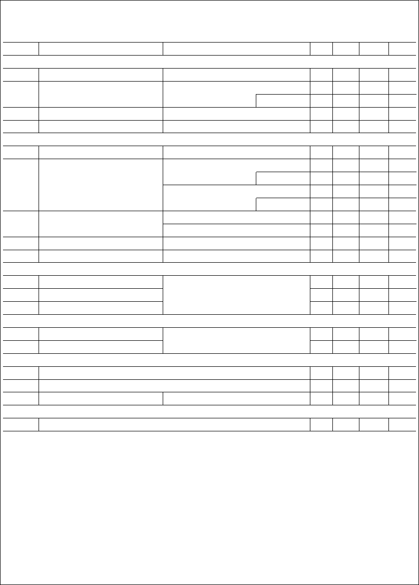
2N7002
Electrical Characteristics TCe25§C unless otherwise noted
Symbol Parameter Conditions Min Typ Max Units
OFF CHARACTERISTICS
BVDSS Drain-Source Breakdown Voltage VGS e0V, IDe10 mA60V
I
DSS Zero Gate Voltage Drain Current VDS e60V, VGS e0V 1 mA
TCe125§C 500 mA
IGSSF Gate-Body Leakage, Forward VGS e20V 100 nA
IGSSR Gate-Body Leakage, Reverse VGS eb
20V b100 nA
ON CHARACTERISTICS*
VGS(th) Gate Threshold Voltage VDS eVGS,I
De
250 mA 1 2.1 2.5 V
rDS(ON) Static Drain-Source VGS e10V, IDe0.5A 1.2 7.5 X
On-Resistance TCe125§C 2 13.5 X
VGS e5V, IDe50 mA 1.7 7.5 X
TCe125§C 2.8 13.5 X
VDS(ON) Drain-Source On-Voltage VGS e10V, IDe0.5A 0.6 3.75 V
VGS e5V, IDe50 mA 0.09 1.5 V
ID(ON) On-State Drain Current VGS e10V, VDS t2V
DS(ON) 500 2700 mA
gFS Forward Transconductance VDS t2V
DS(ON),I
De200 mA 80 320 ms
DYNAMIC CHARACTERISTICS
Ciss Input Capacitance VDS e25V, VGS e0V, f e1.0 MHz 20 50 pF
Coss Output Capacitance 11 25 pF
Crss Reverse Transfer Capacitance 4 5 pF
SWITCHING CHARACTERISTICS*
tON Turn-On Time VDD e30V, IDe200 mA, VGS e10V, 20 ns
tOFF Turn-Off Time RGEN e25X,R
Le150X20 ns
BODY-DRAIN DIODE RATINGS
ISMaximum Continuous Drain-Source Diode Forward Current 115 mA
ISM Maximum Pulsed Drain-Source Diode Forward Current 800 mA
VSD*Drain-Source Diode Forward Voltage VGS e0V, ISe115 mA 1.5 V
THERMAL CHARACTERISTICS
RiJA Thermal Resistance, Junction to Ambient 625 §C/W
*Pulse Test: Pulse Width s300 ms, Duty Cycle s2.0%.
3
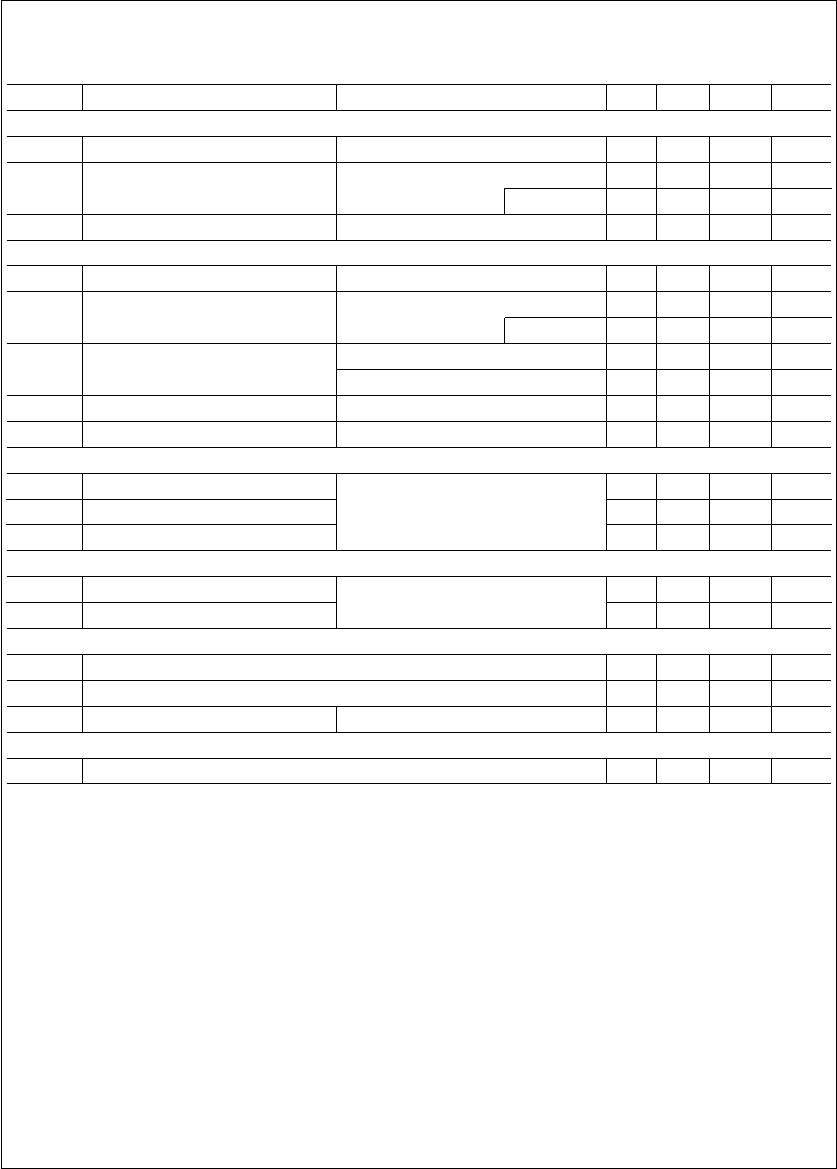
NDF7000A
Electrical Characteristics TCe25§C unless otherwise noted
Symbol Parameter Conditions Min Typ Max Units
OFF CHARACTERISTICS
BVDSS Drain-Source Breakdown Voltage VGS e0V, IDe10 mA60 V
I
DSS Zero Gate Voltage Drain Current VDS e48V, VGS e0V 1 mA
TCe125§C1mA
I
GSSF Gate-Body Leakage, Forward VGS eb
15V b10 nA
ON CHARACTERISTICS*
VGS(th) Gate Threshold Voltage VDS eVGS,I
De1 mA 0.8 2.1 3 V
rDS(ON) Static Drain-Source VGS e10V, IDe0.5A 1.2 2 X
On-Resistance TCe125§C 2 3.5 X
VDS(ON) Drain-Source On-Voltage VGS e10V, IDe500 mA 0.6 1 V
VGS e4.5V, IDe75 mA 0.14 0.225 V
ID(ON) On-State Drain Current VGS e4.5V, VDS t2V
DS(ON) 400 600 mA
gFS Forward Transconductance VDS t2V
DS(ON),I
De200 mA 100 320 ms
DYNAMIC CHARACTERISTICS
Ciss Input Capacitance VDS e25V, VGS e0V, f e1.0 MHz 20 60 pF
Coss Output Capacitance 11 25 pF
Crss Reverse Transfer Capacitance 4 5 pF
SWITCHING CHARACTERISTICS*
ton Turn-On Time VDD e15V, IDe500 mA, VGS e10V, 10 ns
toff Turn-Off Time RGe25X,R
Le25X10 ns
BODY-DRAIN DIODE RATINGS
ISMaximum Continuous Drain-Source Diode Forward Current 400 mA
ISM Maximum Pulsed Drain-Source Diode Forward Current 2000 mA
VSD*Drain-Source Diode Forward Voltage VGS e0V, ISe400 mA 0.88 1.2 V
THERMAL CHARACTERISTICS
RiJA Thermal Resistance, Junction to Ambient 200 §C/W
*Pulse Test: Pulse Width s300 ms, Duty Cycle s2.0%.
4

NDS7002A
Electrical Characteristics TCe25§C unless otherwise noted
Symbol Parameter Conditions Min Typ Max Units
OFF CHARACTERISTICS
BVDSS Drain-Source Breakdown Voltage VGS e0V, IDe10 mA60V
I
DSS Zero Gate Voltage Drain Current VDS e60V, VGS e0V 1 mA
TCe125§C 500 mA
IGSSF Gate-Body Leakage, Forward VGS e20V 100 nA
IGSSR Gate-Body Leakage, Reverse VGS eb
20V b100 nA
ON CHARACTERISTICS*
VGS(th) Gate Threshold Voltage VDS eVGS,I
De
250 mA 1 2.1 2.5 V
rDS(ON) Static Drain-Source VGS e10V, IDe0.5A 1.2 2 X
On-Resistance TCe125§C 2 3.5 X
VGS e5V, IDe50 mA 1.7 3 X
TCe125§C 2.8 5 X
VDS(ON) Drain-Source On-Voltage VGS e10V, IDe500 mA 0.6 1 V
VGS e5.0V, IDe50 mA 0.09 0.15 V
ID(ON) On-State Drain Current VGS e10V, VDS t2V
DS(ON) 500 2700 mA
gFS Forward Transconductance VDS t2V
DS(ON),I
De200 mA 80 320 ms
DYNAMIC CHARACTERISTICS
Ciss Input Capacitance VDS e25V, VGS e0V, f e1.0 MHz 20 50 pF
Coss Output Capacitance 11 25 pF
Crss Reverse Transfer Capacitance 4 5 pF
SWITCHING CHARACTERISTICS*
tON Turn-On Time VDD e30V, IDe200 mA, VGS e10V, 20 ns
tOFF Turn-Off Time RGe25X,R
Le150X20 ns
BODY-DRAIN DIODE RATINGS
ISMaximum Continuous Drain-Source Diode Forward Current 280 mA
ISM Maximum Pulsed Drain-Source Diode Forward Current 1500 mA
VSD*Drain-Source Diode Forward Voltage VGS e0V, ISe400 mA 0.88 1.2 V
THERMAL CHARACTERISTICS
RiJA Thermal Resistance, Junction to Ambient 417 §C/W
*Pulse Test: Pulse Width s300 ms, Duty Cycle s2.0%.
5
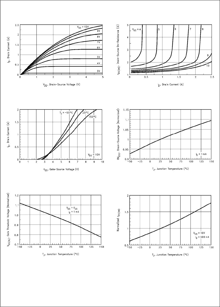
Typical Electrical Characteristics
2N7000/2N7002/NDF7000A/NDS7002A
TL/G/11378–4
FIGURE 1. On-Region Characteristics
TL/G/11378–5
FIGURE 2. rDS(ON) Variation
with Drain Current and Gate Voltage
TL/G/11378–6
FIGURE 3. Transfer Characteristics
TL/G/11378–7
FIGURE 4. Breakdown Voltage
Variation with Temperature
TL/G/11378–8
FIGURE 5. Gate Threshold Variation with Temperature
TL/G/11378–9
FIGURE 6. On-Resistance Variation with Temperature
6
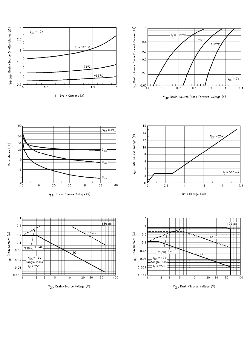
Typical Electrical Characteristics (Continued)
2N7000/2N7002/NDF7000A/NDS7002A (Continued)
TL/G/11378–10
FIGURE 7. On-Resistance vs Drain Current
TL/G/11378–11
FIGURE 8. Body Diode Forward Voltage
Variation with Current and Temperature
TL/G/11378–12
FIGURE 9. Capacitance vs Drain-Source Voltage
TL/G/11378–13
FIGURE 10. Gate Charge vs Gate-Source Voltage
TL/G/11378–14
FIGURE 11. 2N7000 Safe Operating Area
TL/G/11378–15
FIGURE 12. 2N7002 Safe Operating Area
7
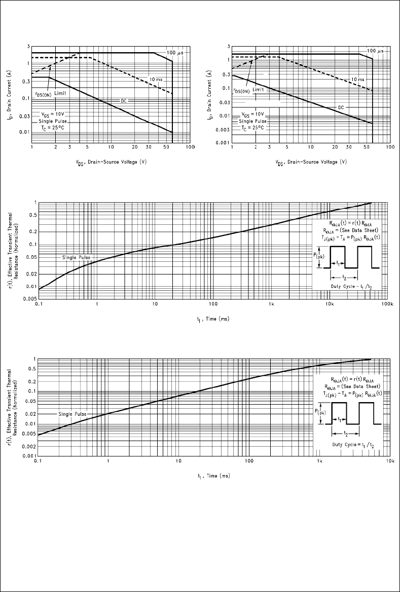
Typical Electrical Characteristics (Continued)
2N7000/2N7002/NDF7000A/NDS7002A (Continued)
TL/G/11378–16
FIGURE 13. NDF7000A Safe Operating Area
TL/G/11378–17
FIGURE 14. NDS7002A Safe Operating Area
TL/G/11378–18
FIGURE 15. TO-92 Transient Thermal Response
TL/G/11378–19
FIGURE 16. SOT-23 Transient Thermal Response
8
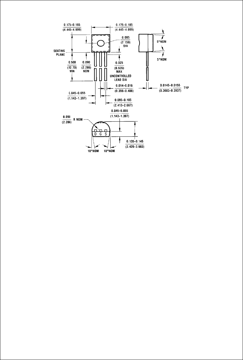
Physical Dimensions inches (millimeters)
TL/G/11378–20
TO-92
9
2N7000/2N7002/NDF7000A/NDS7002A N-Channel Enhancement Mode Field Effect Transistor
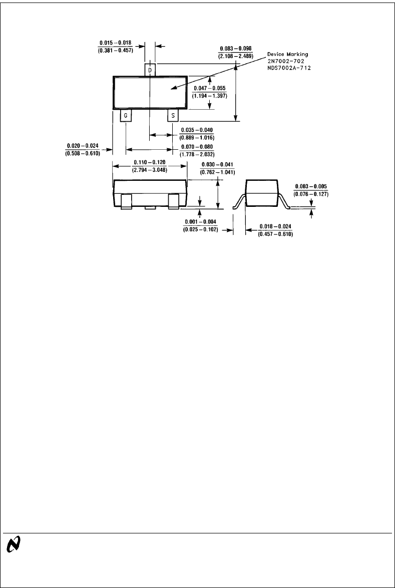
Physical Dimensions inches (millimeters) (Continued)
TL/G/11378–21
Note 1: Meets all JEDEC dimensional requirements for TO-236AB.
Note 2: Controlling dimension: millimeters.
Note 3: Available also in TO-236AA. Contact your local National Semiconductor representative for delivery and ordering information.
Note 4: Tape and reel is the standard packaging method for TO-236.
TO-236AB (SOT-23) (Notes 3, 4)
LIFE SUPPORT POLICY
NATIONAL’S PRODUCTS ARE NOT AUTHORIZED FOR USE AS CRITICAL COMPONENTS IN LIFE SUPPORT
DEVICES OR SYSTEMS WITHOUT THE EXPRESS WRITTEN APPROVAL OF THE PRESIDENT OF NATIONAL
SEMICONDUCTOR CORPORATION. As used herein:
1. Life support devices or systems are devices or 2. A critical component is any component of a life
systems which, (a) are intended for surgical implant support device or system whose failure to perform can
into the body, or (b) support or sustain life, and whose be reasonably expected to cause the failure of the life
failure to perform, when properly used in accordance support device or system, or to affect its safety or
with instructions for use provided in the labeling, can effectiveness.
be reasonably expected to result in a significant injury
to the user.
National Semiconductor National Semiconductor National Semiconductor National Semiconductor
Corporation Europe Hong Kong Ltd. Japan Ltd.
1111 West Bardin Road Fax: (
a
49) 0-180-530 85 86 13th Floor, Straight Block, Tel: 81-043-299-2309
Arlington, TX 76017 Email: cnjwge
@
tevm2.nsc.com Ocean Centre, 5 Canton Rd. Fax: 81-043-299-2408
Tel: 1(800) 272-9959 Deutsch Tel: (
a
49) 0-180-530 85 85 Tsimshatsui, Kowloon
Fax: 1(800) 737-7018 English Tel: (
a
49) 0-180-532 78 32 Hong Kong
Fran3ais Tel: (
a
49) 0-180-532 93 58 Tel: (852) 2737-1600
Italiano Tel: (
a
49) 0-180-534 16 80 Fax: (852) 2736-9960
National does not assume any responsibility for use of any circuitry described, no circuit patent licenses are implied and National reserves the right at any time without notice to change said circuitry and specifications.
