2N7002 Datasheet. Www.s Manuals.com. Calogic
User Manual: Marking of electronic components, SMD Codes V0, V0**, V0-***, V00, V02, V08, V0=***. Datasheets 2N7002, 74LVC1G00GV, 74LVC1G08GV, RT9271GB, RT9271PB, TC74A0-3.3VCT, TZT2V4CW.
Open the PDF directly: View PDF ![]() .
.
Page Count: 3
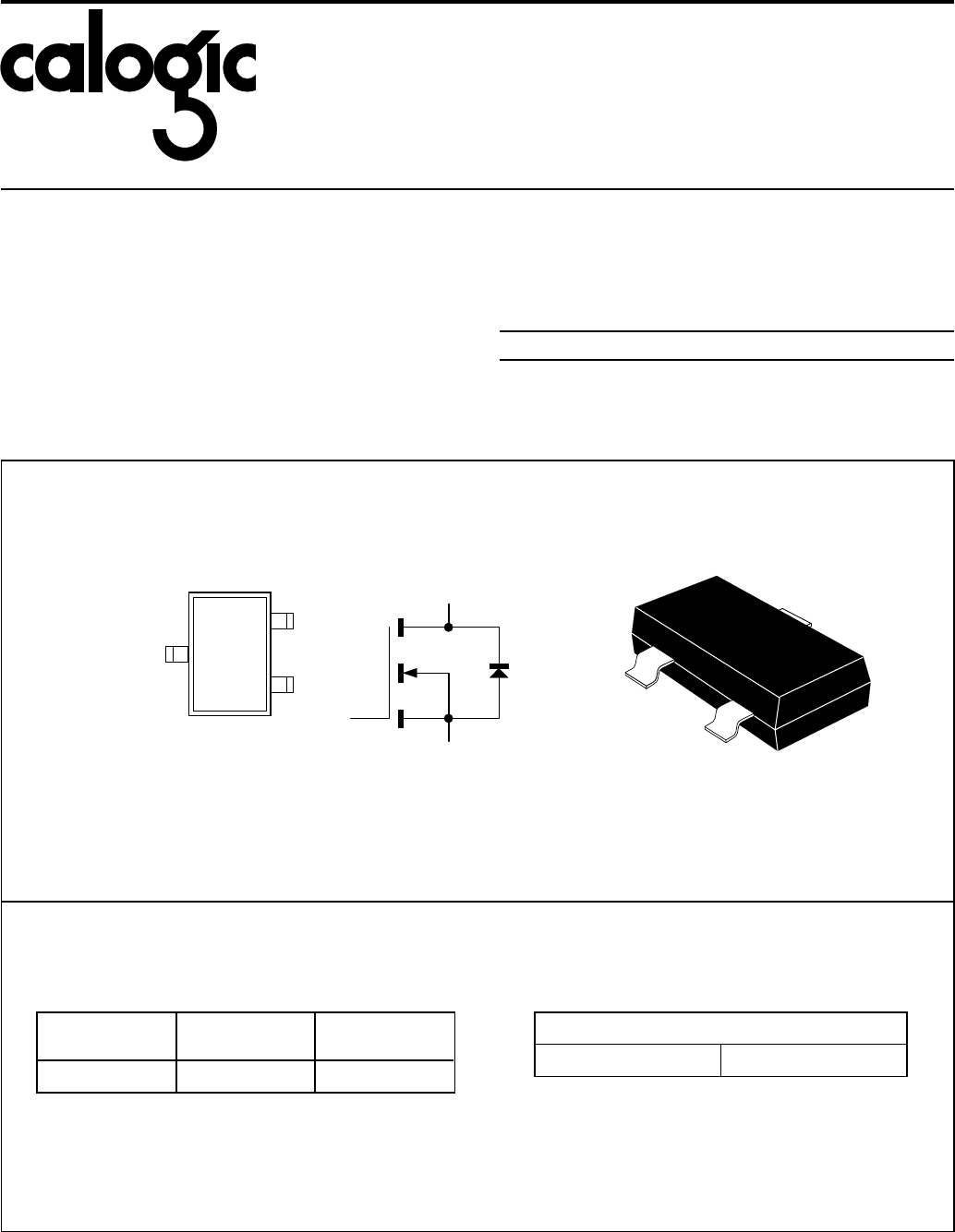
N-Channel Enhancement-Mode
MOS Transistor
2N7002
DESCRIPTION
Calogic’s 2N7002 device type is a vertical DMOS FET
transistor housed in a surface mount SOT-23 for
micro-assembly applications. The device is an excellent
choice for switching applications where breakdown (BV) and
low on-resistance are important.
ORDERING INFORMATION
Part Package Temperature Range
2N7002 Plastic SOT-23 Package -55oC to +150oC
X2N7002 Sorted Chips in Carriers -55oC to +150oC
CORPORATION
D
G
S
SOT-23
1
2
3
TOP VIEW
1
2
3
DRAIN
SOURCE
GATE
1
2
3
PIN CONFIGURATION
PRODUCT SUMMARY
V(BR)DSS
(V) rDS(ON)
(Ω)ID
(A)
60 7.5 0.115
PRODUCT MARKING
2N7002 V02
CD5
9-3
2N7002
CORPORATION
ABSOLUTE MAXIMUM RATINGS (TA = 25oC unless otherwise specified)
SYMBOL PARAMETERS LIMITS UNITS TEST CONDITIONS
VDS Drain-Source Voltage 60 V
VGS Gate-Source Voltage ±40
IDContinuous Drain Current 0.115
A
TA = 25oC
0.073 TA = 100oC
IDM Pulsed Drain Current10.8
PDPower Dissipation 200 mW TA = 25oC
80 TA = 100oC
TJOperating Junction Temperature Range -55 to 150
oCTstg Storage Temperature Range -55 to 150
TLLead Temperature (1/16" from case for 10 sec.) 300
THERMAL RESISTANCE RATINGS
SYMBOL THERMAL RESISTANCE LIMITS UNITS
RthJA Junction-to-Ambient 625 K/W
NOTE: 1. Pulse width limited by maximum junction temperature.
SPECIFICATIONS1
SYMBOL PARAMETER MIN TYP2MAX UNIT TEST CONDITIONS
STATIC
V(BR)DSS Drain-Source Breakdown Voltage 60 70 VID = 10µA, VGS = 0V
VGS(th) Gate-Threshold Voltage 1 1.9 2.5 VDS = VGS, ID = 0.25mA
IGSS Gate-Body Leakage ±100 nA VGS = ±20V, VDS = 0V
IDSS Zero Gate Voltage Drain Current 1µAVDS = 60V, VGS = 0V
500 TC = 125oC
ID(ON) On-State Drain Current3500 1000 mA VDS = ≥2VDS(ON), VGS = 10V
rDS(ON) Drain-Source On-Resistance3
57.5
Ω
VGS = 5V, ID = 50mA
913.5 TC = 125oC
2.5 7.5 VGS = 10V, ID = 0.5A
4.4 13.5 TC = 125oC
VDS(ON) Drain-Source On-Voltage3
0.25 0.375
V
VGS = 5V, ID = 50mA
1.25 3.75 VGS = 10V, ID = 0.5A
2.2 6.75 TC = 125oC4
gFS Forward Transconductance380 170 mS VDS = 10V, ID = 0.2A
gOS Common Source Output Conductance3, 4 500 µSVDS = 5V, ID = 50mA
DYNAMIC
Ciss Input Capacitance 16 50
pF VDS = 25V, VGS = 0V, f = 1MHzCoss Output Capacitance411 25
Crss Reverse Transfer Capacitance 25
SWITCHING
tON Turn-On Time 7 20
nS
VDD = 30V, RL = 150Ω, ID = 0.2A
VGEN = 10V, RG = 25Ω
(Switching time is essentially
independent of operating temperature)
tOFF Turn-Off Time 720
NOTES: 1. TA = 25oC unless otherwise specified.
2. For design aid only, not subject to production testing.
3. Pulse test; PW = ≤80µS, duty cycle ≤1%.
4. This parameter not registered with JEDEC.
9-4