2N7002E Datasheet. Www.s Manuals.com. On
User Manual: Marking of electronic components, SMD Codes 7002, 7005, 702, 702⚫, 702*, 703 *, 7030L, 704, 705, 709, 709**, 70N10L, 70T. Datasheets 2N7002, 2N7002-G, 2N7002DW, 2N7002E, 2N7002K, 2N7002L, 2N7002MTF, 2V7002K, 2V7002L, FAN7005M, FCX705, G709RCUf, G709T1Uf, L2N7002LT1G, MTN138ZN3, MTN7002N3, MTN7002ZHN3, MTNK1N3, MTNK2N3, PH7030L, SPB70N10L, SPI70N10L, SPP70N10L, TK71570AS.
Open the PDF directly: View PDF ![]() .
.
Page Count: 6
© Semiconductor Components Industries, LLC, 2011
February, 2011 − Rev. 3
1Publication Order Number:
2N7002E/D
2N7002E
Small Signal MOSFET
60 V, 310 mA, Single, N−Channel, SOT−23
Features
•Low RDS(on)
•Small Footprint Surface Mount Package
•Trench Technology
•These Devices are Pb−Free, Halogen Free/BFR Free and are RoHS
Compliant
Applications
•Low Side Load Switch
•Level Shift Circuits
•DC−DC Converter
•Portable Applications i.e. DSC, PDA, Cell Phone, etc.
MAXIMUM RATINGS (TJ = 25°C unless otherwise stated)
Rating Symbol Value Unit
Drain−to−Source Voltage VDSS 60 V
Gate−to−Source Voltage VGS ±20 V
Drain Current (Note 1)
Steady State TA = 25°C
TA = 85°C
t < 5 s TA = 25°C
TA = 85°C
ID260
190
310
220
mA
Power Dissipation (Note 1)
Steady State
t < 5 s
PD300
420
mW
Pulsed Drain Current (tp = 10 ms) IDM 1.2 A
Operating Junction and Storage
Temperature Range
TJ, TSTG −55 to
+150
°C
Source Current (Body Diode) IS300 mA
Lead Temperature for Soldering Purposes
(1/8″ from case for 10 s)
TL260 °C
Stresses exceeding Maximum Ratings may damage the device. Maximum
Ratings are stress ratings only. Functional operation above the Recommended
Operating Conditions is not implied. Extended exposure to stresses above the
Recommended Operating Conditions may affect device reliability.
THERMAL CHARACTERISTICS
Characteristic Symbol Max Unit
Junction−to−Ambient − Steady State
(Note 1)
RqJA 417 °C/W
Junction−to−Ambient − t ≤ 5 s (Note 1) RqJA 300
1. Surface−mounted on FR4 board using 1 in sq pad size (Cu area = 1.127 in
sq [1 oz] including traces)
Device Package Shipping†
ORDERING INFORMATION
2N7002ET1G 3000/Tape & Reel
Simplified Schematic
SOT−23
CASE 318
STYLE 21
703 MG
G
703 = Device Code
M = Date Code
G= Pb−Free Package
MARKING DIAGRAM
& PIN ASSIGNMENT
3
21
Drain
Gate
2
1
3
Source
http://onsemi.com
SOT−23
(Pb−Free)
60 V 3.0 W @ 4.5 V
RDS(on) MAX
310 mA
ID MAX
(Note 1)
V(BR)DSS
†For information on tape and reel specifications,
including part orientation and tape sizes, please
refer to our Tape and Reel Packaging Specifications
Brochure, BRD8011/D.
2.5 W @ 10 V
(Top View)
3
1
2
N−Channel
(Note: Microdot may be in either location)
2N7002E
http://onsemi.com
2
ELECTRICAL CHARACTERISTICS (TJ = 25°C unless otherwise specified)
Parameter Symbol Test Condition Min Typ Max Units
OFF CHARACTERISTICS
Drain−to−Source Breakdown Voltage V(BR)DSS VGS = 0 V, ID = 250 mA60 V
Drain−to−Source Breakdown Voltage
Temperature Coefficient
V(BR)DSS/TJ75 mV/°C
Zero Gate Voltage Drain Current IDSS VGS = 0 V,
VDS = 60 V
TJ = 25°C 1 mA
TJ = 125°C 500
Gate−to−Source Leakage Current IGSS VDS = 0 V, VGS = ±20 V ±100 nA
ON CHARACTERISTICS (Note 2)
Gate Threshold Voltage VGS(TH) VGS = VDS, ID = 250 mA1.0 2.5 V
Negative Threshold Temperature
Coefficient
VGS(TH)/TJ4.4 mV/°C
Drain−to−Source On Resistance RDS(on) VGS = 10 V, ID = 240 mA 0.86 2.5 W
VGS = 4.5 V, ID = 50 mA 1.1 3.0
Forward Transconductance gFS VDS = 5 V, ID = 200 mA 530 mS
CHARGES AND CAPACITANCES
Input Capacitance CISS
VGS = 0 V, f = 1 MHz,
VDS = 25 V
26.7 40 pF
Output Capacitance COSS 4.6
Reverse Transfer Capacitance CRSS 2.9
Total Gate Charge QG(TOT)
VGS = 5 V, VDS = 10 V;
ID = 240 mA
0.81 nC
Threshold Gate Charge QG(TH) 0.31
Gate−to−Source Charge QGS 0.48
Gate−to−Drain Charge QGD 0.08
SWITCHING CHARACTERISTICS, VGS = V (Note 3)
Turn−On Delay Time td(ON)
VGS = 10 V, VDD = 30 V,
ID = 200 mA, RG = 10 W
1.7 ns
Rise Time tr1.2
Turn−Off Delay Time td(OFF) 4.8
Fall Time tf3.6
DRAIN−SOURCE DIODE CHARACTERISTICS
Forward Diode Voltage VSD VGS = 0 V,
IS = 200 mA
TJ = 25°C 0.79 1.2 V
TJ = 85°C 0.7
2. Pulse Test: pulse width ≤ 300 ms, duty cycle ≤ 2%
3. Switching characteristics are independent of operating junction temperatures
2N7002E
http://onsemi.com
3
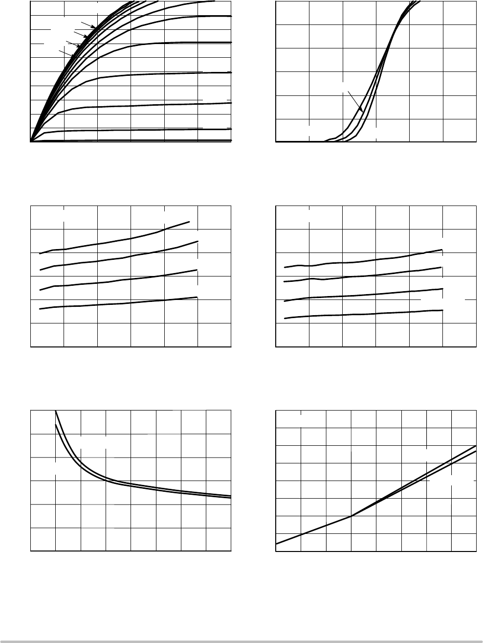
TYPICAL CHARACTERISTICS
Figure 1. On−Region Characteristics Figure 2. Transfer Characteristics
VDS, DRAIN−TO−SOURCE VOLTAGE (V) VGS, GATE−TO−SOURCE VOLTAGE (V)
6420
0
0.4
0.8
1.2
1.6
2.0
6420
0
0.4
0.8
1.2
Figure 3. On−Resistance vs. Drain Current and
Temperature
Figure 4. On−Resistance vs. Drain Current and
Temperature
ID, DRAIN CURRENT (A)
1.21.00.80.60.40.20
0
0.4
0.8
1.2
1.6
2.0
2.4
Figure 5. On−Resistance vs. Gate−to−Source
Voltage
Figure 6. On−Resistance Variation with
Temperature
VGS, GATE−TO−SOURCE VOLTAGE (V) TJ, JUNCTION TEMPERATURE (°C)
108642
0.4
0.8
1.2
1.6
1251007550250−25−50
0.6
1.0
1.4
1.8
2.2
ID, DRAIN CURRENT (A)
ID, DRAIN CURRENT (A)
RDS(on), DRAIN−TO−SOURCE RESISTANCE (W)RDS(on), DRAIN−TO−SOURCE RESISTANCE (W)
RDS(on), DRAIN−TO−SOURCE
RESISTANCE (NORMALIZED)
VGS = 10 V 5.0 V
7.0 V
8.0 V
9.0 V 4.5 V
4.0 V
6.0 V
3.5 V
3.0 V
2.5 V
2.0 V TJ = −55°C
TJ = 125°C
TJ = 25°C
TJ = −55°C
TJ = 125°C
TJ = 25°C
TJ = 85°C
VGS = 4.5 V
ID, DRAIN CURRENT (A)
1.21.00.80.60.40.20
0
0.4
0.8
1.2
1.6
2.0
2.4
RDS(on), DRAIN−TO−SOURCE RESISTANCE (W)
TJ = −55°C
TJ = 125°C
TJ = 25°C
TJ = 85°C
VGS = 10 V
ID = 250 mA
ID = 75 mA
150
ID = 0.2 A
VGS = 4.5 V
VGS = 10 V
2N7002E
http://onsemi.com
4
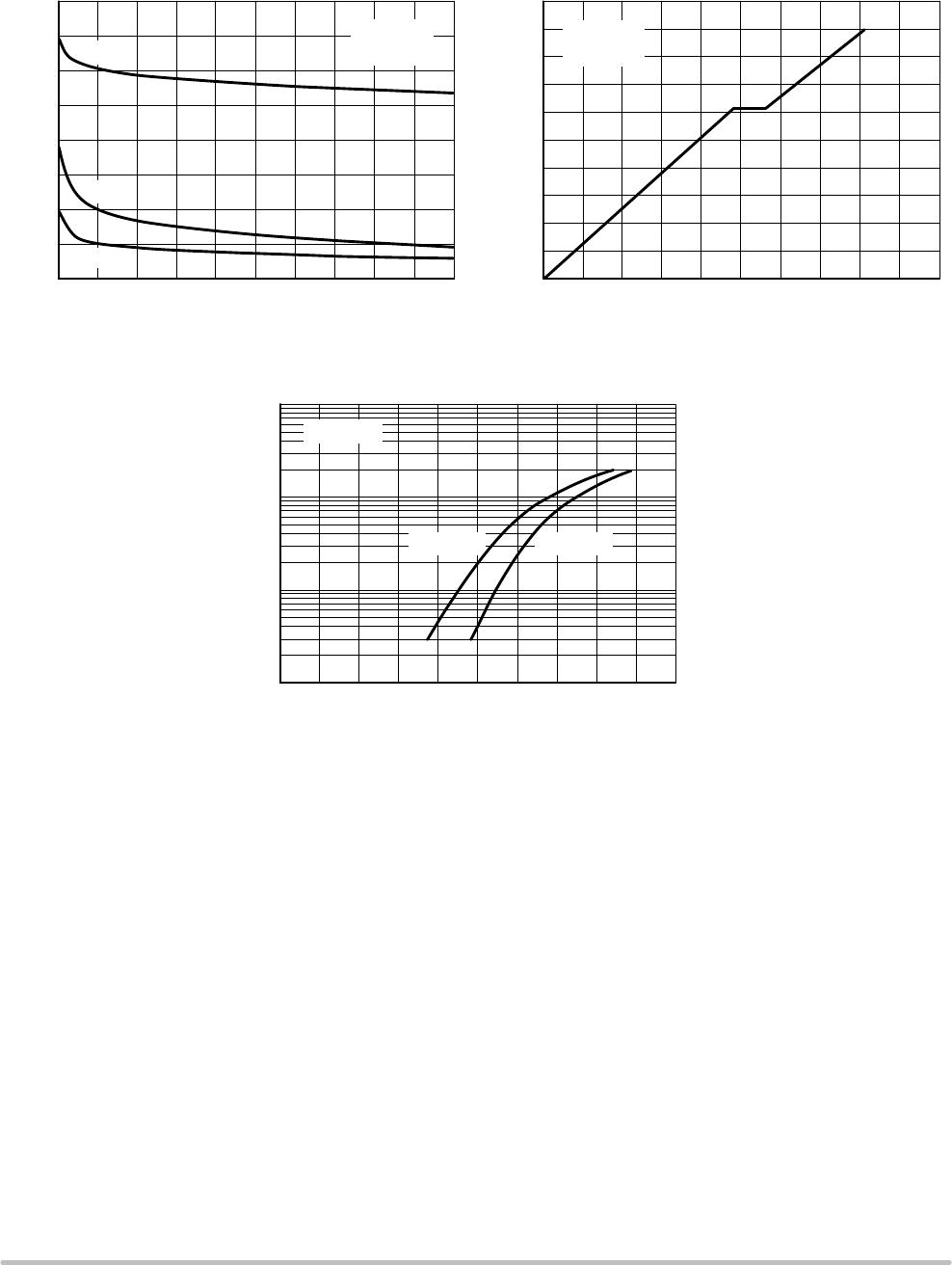
TYPICAL CHARACTERISTICS
Figure 7. Capacitance Variation Figure 8. Gate−to−Source and
Drain−to−Source Voltage vs. Total Charge
Qg, TOTAL GATE CHARGE (nC)
10.80.60.40.20
0
1
2
3
4
5
Figure 9. Diode Forward Voltage vs. Current
VSD, SOURCE−TO−DRAIN VOLTAGE (V)
1.21.00.80.60.40.2
0.01
1
10
VGS, GATE−TO−SOURCE VOLTAGE (V)
IS, SOURCE CURRENT (A)
TJ = 25°C
ID = 0.25 A
201612840
0
10
20
30
40
C, CAPACITANCE (pF)
Ciss
Coss
Crss
TJ = 25°C
VGS = 0 V
GATE−TO−SOURCE OR DRAIN−TO−SOURCE VOLTAGE (V)
TJ = 25°CTJ = 85°C
VGS = 0 V
0.1
2N7002E
http://onsemi.com
5
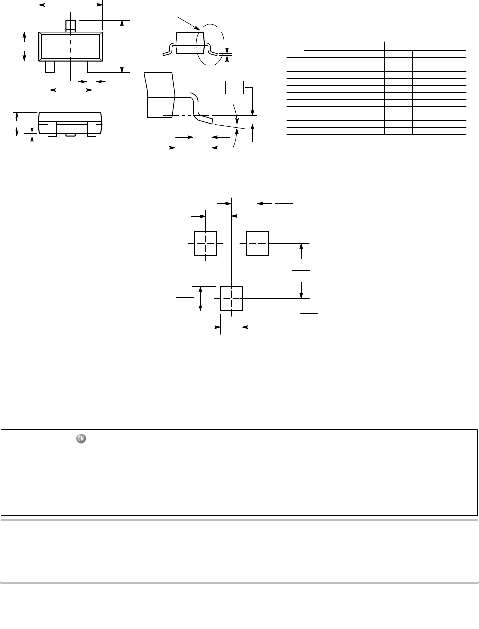
PACKAGE DIMENSIONS
SOT−23 (TO−236)
CASE 318−08
ISSUE AP
STYLE 21:
PIN 1. GATE
2. SOURCE
3. DRAIN
D
A1
3
12
NOTES:
1. DIMENSIONING AND TOLERANCING PER ANSI Y14.5M, 1982.
2. CONTROLLING DIMENSION: INCH.
3. MAXIMUM LEAD THICKNESS INCLUDES LEAD FINISH
THICKNESS. MINIMUM LEAD THICKNESS IS THE MINIMUM
THICKNESS OF BASE MATERIAL.
4. DIMENSIONS D AND E DO NOT INCLUDE MOLD FLASH,
PROTRUSIONS, OR GATE BURRS.
ǒmm
inchesǓ
SCALE 10:1
0.8
0.031
0.9
0.035
0.95
0.037
0.95
0.037
2.0
0.079
SOLDERING FOOTPRINT
VIEW C
L
0.25
L1
q
e
EE
b
A
SEE VIEW C
DIM
A
MIN NOM MAX MIN
MILLIMETERS
0.89 1.00 1.11 0.035
INCHES
A1 0.01 0.06 0.10 0.001
b0.37 0.44 0.50 0.015
c0.09 0.13 0.18 0.003
D2.80 2.90 3.04 0.110
E1.20 1.30 1.40 0.047
e1.78 1.90 2.04 0.070
L0.10 0.20 0.30 0.004
0.040 0.044
0.002 0.004
0.018 0.020
0.005 0.007
0.114 0.120
0.051 0.055
0.075 0.081
0.008 0.012
NOM MAX
L1
H
2.10 2.40 2.64 0.083 0.094 0.104
HE
0.35 0.54 0.69 0.014 0.021 0.029
c
0−−− 10 0 −−− 10
q°°°°
ON Semiconductor and are registered trademarks of Semiconductor Components Industries, LLC (SCILLC). SCILLC reserves the right to make changes without further notice
to any products herein. SCILLC makes no warranty, representation or guarantee regarding the suitability of its products for any particular purpose, nor does SCILLC assume any liability
arising out of the application or use of any product or circuit, and specifically disclaims any and all liability, including without limitation special, consequential or incidental damages.
“Typical” parameters which may be provided in SCILLC data sheets and/or specifications can and do vary in different applications and actual performance may vary over time. All
operating parameters, including “Typicals” must be validated for each customer application by customer’s technical experts. SCILLC does not convey any license under its patent rights
nor the rights of others. SCILLC products are not designed, intended, or authorized for use as components in systems intended for surgical implant into the body, or other applications
intended to support or sustain life, or for any other application in which the failure of the SCILLC product could create a situation where personal injury or death may occur. Should Buyer
purchase or use SCILLC products for any such unintended or unauthorized application, Buyer shall indemnify and hold SCILLC and its officers, employees, subsidiaries, affiliates,
and distributors harmless against all claims, costs, damages, and expenses, and reasonable attorney fees arising out of, directly or indirectly, any claim of personal injury or death
associated with such unintended or unauthorized use, even if such claim alleges that SCILLC was negligent regarding the design or manufacture of the part. SCILLC is an Equal
Opportunity/Affirmative Action Employer. This literature is subject to all applicable copyright laws and is not for resale in any manner.
PUBLICATION ORDERING INFORMATION
N. American Technical Support: 800−282−9855 Toll Free
USA/Canada
Japan: ON Semiconductor, Japan Customer Focus Center
2−9−1 Kamimeguro, Meguro−ku, Tokyo, Japan 153−0051
Phone: 81−3−5773−3850
2N7002E/D
LITERATURE FULFILLMENT:
Literature Distribution Center for ON Semiconductor
P.O. Box 5163, Denver, Colorado 80217 USA
Phone: 303−675−2175 or 800−344−3860 Toll Free USA/Canada
Fax: 303−675−2176 or 800−344−3867 Toll Free USA/Canada
Email: orderlit@onsemi.com
ON Semiconductor Website: http://onsemi.com
Order Literature: http://www.onsemi.com/litorder
For additional information, please contact your
local Sales Representative.