2N7002T Datasheet. Www.s Manuals.com. Fairchild
User Manual: Marking of electronic components, SMD Codes AA, AA**, AA***, AA-, AA-**, AA-***, AA=***, AAA, AAA***, AAC, AAD, AAE, AAE**, AAF, AAFI, AAG, AAH**, AAHC, AAHO, AAI**, AAIK, AAJ**, AAJ***, AAJF*, AAJI, AAJJ, AAL***, AAM***, AAN***, AANC, AAP, AAQ, AAR, AAS, AASQ, AASR, AAT***, AATJ, AATK, AATL, AATM, AAU, AAU**, AAW, AAX, Aa. Datasheets 2N7002T, 2SD1757K, 74AHC1G00GW, AME8804AEEY, BCW60A, BCX51, BD48E23G, BD48K23G, BL3406B-1.0V, BL9641, LR9641, MAX1736EUT41-T, MAX1736EUT42-T, MAX2644, MAX4335EXT-T, MAX4336EXT
Open the PDF directly: View PDF ![]() .
.
Page Count: 7
2N7002T — N-Channel Enhancement Mode Field Effect Transistor
© 2007 Fairchild Semiconductor Corporation www.fairchildsemi.com
2N7002T Rev. A 1
October 2007
2N7002T
N-Channel Enhancement Mode Field Effect Transistor
Features
• Low On-Resistance
• Low Gate Threshold Voltage
• Low Input Capacitance
• Fast Switching Speed
• Low Input/Output Leakage
• Ultra-Small Surface Mount Package
• Lead Free/RoHS Compliant
Absolute Maximum Ratings * Ta = 25°C unless otherwise noted
* These ratings are limiting values above which the serviceability of any semiconductor device may by impaired.
Thermal Characteristics
* Device mounted on FR-4 PCB, 1 inch x 0.85 inch x 0.062 inch. Minimun land pad size,
Symbol Parameter Value Units
VDSS Drain-Source Voltage 60 V
VDGR Drain-Gate Voltage RGS ≤ 1.0MΩ 60 V
VGSS Gate-Source Voltage Continuous
Pulsed
±20
±40 V
ID Drain Current Continuous
Continuous @ 100°C
Pulsed
115
73
800
mA
TJ Junction Temperature 150 °C
TSTG Storage Temperature Range -55 to +150 °C
Symbol Parameter Value Units
PDTotal Device Dissipation
Derating above TA = 25°C
200
1.6
mW
mW/°C
RθJA Thermal Resistance, Junction to Ambient * 625 °C/W
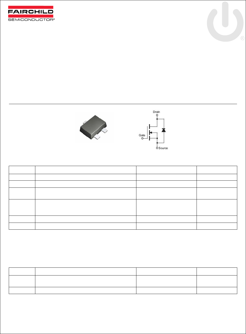
SOT - 523F
S
G
D
Marking : AA
2N7002T — N-Channel Enhancement Mode Field Effect Transistor
© 2007 Fairchild Semiconductor Corporation www.fairchildsemi.com
2N7002T Rev. A 2
Electrical Characteristics TC = 25°C unless otherwise noted
Off Characteristics (Note1)
On Characteristics (Note1)
Dynamic Characteristics
Switching Characteristics
Note1 : Short duration test pulse used to minimize self-heating effect.
Symbol Parameter Test Condition MIN TYP MAX Units
BVDSS Drain-Source Breakdown Voltage VGS= 0V, ID=10uA 60 78 - V
IDSS Zero Gate Voltage Drain Current VDS= 60V, VGS= 0V
VDS= 60V, VGS= 0V, @TC = 125°C
-0.001
7
1.0
500 uA
IGSS Gate-Body Leakage VGS= ±20V, VDS= 0V -0.2 ±10 nA
VGS(th) Gate Threshold Voltage VDS = VGS, ID = 250uA 1.0 1.76 2.0 V
RDS(ON) Satic Drain-Source On-Resistance VGS = 5V, ID = 0.05A,
VGS = 10V, ID = 0.5A, @Tj = 125°C
-
-
1.6
2.53
7.5
13.5 Ω
ID(ON) On-State Drain Current VGS = 10V, VDS= 7.5V 0.5 1.43 - A
gFS Forward Transconductance VDS = 10V, ID = 0.2A 80 356.5 -mS
Ciss Input Capacitance
VDS = 25V, VGS= 0V, f = 1.0MHz
-37.8 50 pF
Coss Output Capacitance -12.4 25 pF
Crss Reverse Transfer Capacitance -6.5 7.0 pF
tD(ON) Turn-On Delay Time VDD = 30V, ID = 0.2A, VGEN= 10V
RL = 150Ω, RGEN = 25Ω
-5.85 20 ns
tD(OFF) Turn-Off Delay Time -12.5 20
2N7002T — N-Channel Enhancement Mode Field Effect Transistor
© 2007 Fairchild Semiconductor Corporation www.fairchildsemi.com
2N7002T Rev. A 3
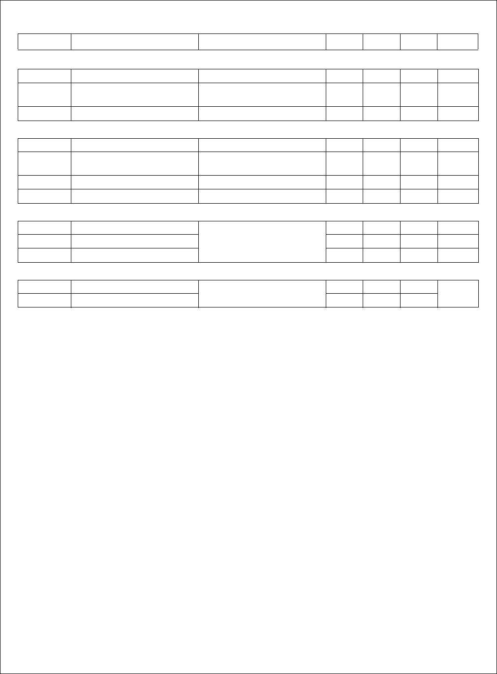
Typical Performance Characteristics
Figure 1. On-Region Characteristics Figure 2. On-Resistance Variation with Gate
Voltage and Drain Current
Figure 3. On-Resistance Variation with
Temperature Figure 4. On-Resistance Variation with
Gate-Source Voltage
Figure 5. Transfer Characteristics Figure 6. Gate Threshold Variation with
Temperature
012345678910
0.0
0.2
0.4
0.6
0.8
1.0
1.2
1.4
1.6
2V
3V
4V
5V
VGS = 10V
ID. DRAIN-SOURCE CURRENT(A)
VDS. DRAIN-SOURCE VOLTAGE (V)
0.0 0.2 0.4 0.6 0.8 1.0
1.0
1.5
2.0
2.5
3.0
(Ω)
9V
8V
5V
6V
10V
7V
4V 4.5V
VGS = 3V
RDS(on),
DRANI-SOURCE ON-RESISTANCE
ID. DRAIN-SOURCE CURRENT(A)
-50 0 50 100 150
0.5
1.0
1.5
2.0
2.5
3.0
(Ω)
VGS = 10V
ID = 500 mA
RDS(on)
DRANI-SOURCE ON-RESISTANCE
TJ. JUNCTION TEMPERATURE(oC)
246810
1.0
1.5
2.0
2.5
3.0
ID = 500 mA
(Ω)
ID = 50 mA
RDS(on),
DRANI-SOURCE ON-RESISTANCE
VGS. GATE-SOURCE VOLTAGE (V)
23456
0.0
0.2
0.4
0.6
0.8
1.0
VDS = 10V
75oC
125oC
150oC
25oC
TJ = -25oC
ID. DRAIN-SOURCE CURRENT(A)
VGS. GATE-SOURCE VOLTAGE (V)
-50 0 50 100 150
1.0
1.5
2.0
2.5
ID = 0.25 mA
ID = 1 mA
VGS = VDS
Vth, Gate-Source Threshold Voltage (V)
TJ. JUNCTION TEMPERATURE(oC)
2N7002T — N-Channel Enhancement Mode Field Effect Transistor
© 2007 Fairchild Semiconductor Corporation www.fairchildsemi.com
2N7002T Rev. A 4
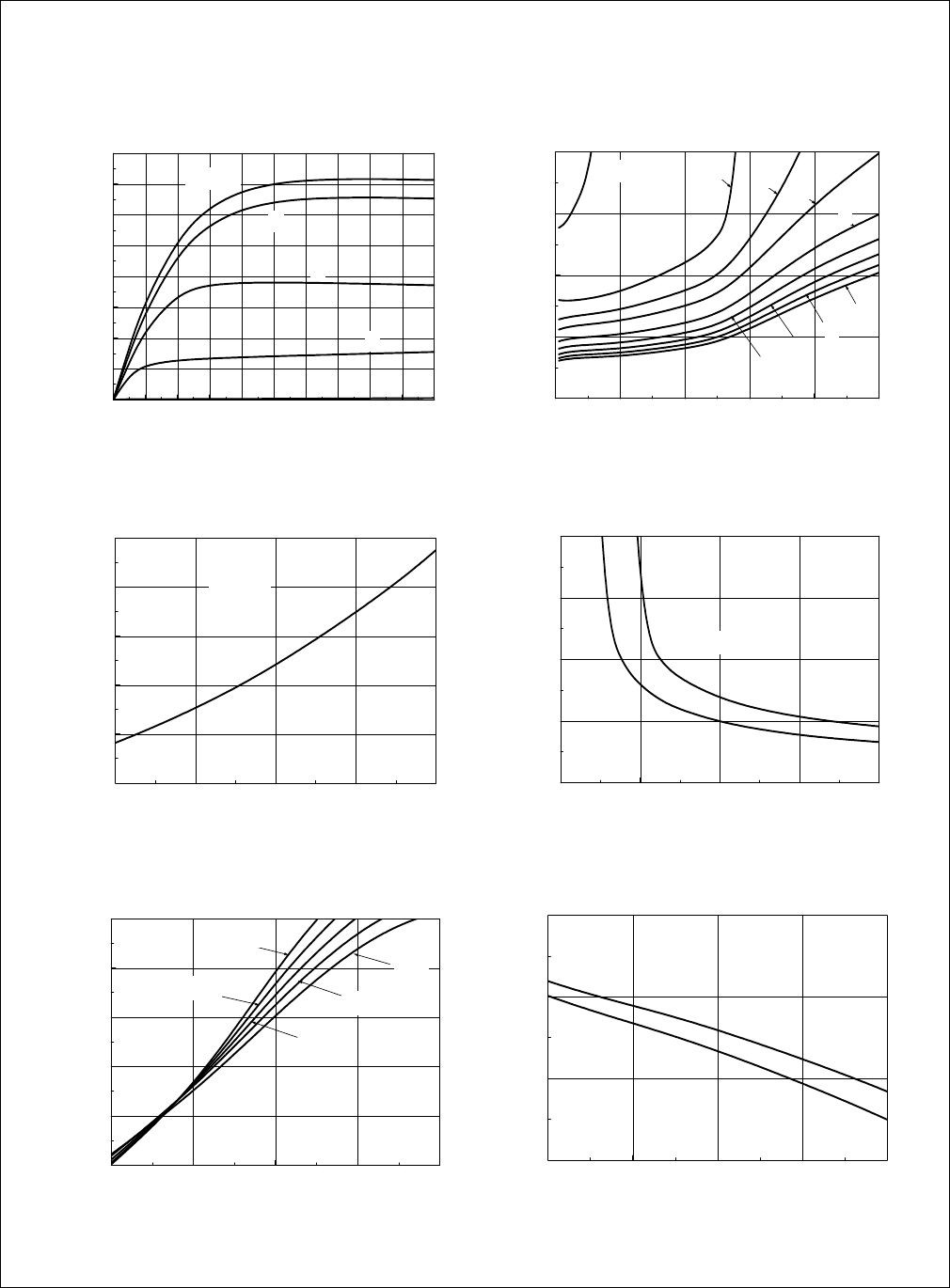
Typical Performance Characteristics
Figure 7. Reverse Drain Current Variation with
Diode Forward Voltage and Temperature Figure 8. Power Derating
1
10
100
0.0 0.2 0.4 0.6 0.8 1.0
-55oC
VGS = 0 V
150oC
25oC
VSD, Body Diode Forward Voltage [V]
IS Reverse Drain Current, [mA]
0 25 50 75 100 125 150 175
0
50
100
150
200
250
PC[mW], POWER DISSIPATION
Ta[oC], AMBIENT TEMPERATURE
2N7002T — N-Channel Enhancement Mode Field Effect Transistor
© 2007 Fairchild Semiconductor Corporation www.fairchildsemi.com
2N7002T Rev. A 5
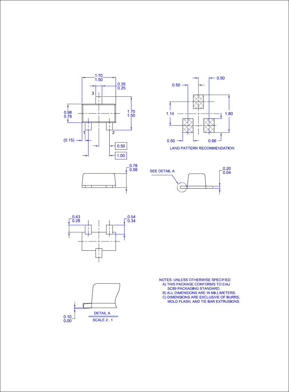
SOT-523F
Package Dimensions
Dimensions in Millimeters

2N7002T N-Channel Enhancement Mode Field Effect Transistor2N7002T
TRADEMARKS
The following are registered and unregistered trademarks and service marks Fairchild Semiconductor owns or is authorized to use and
is not intended to be an exhaustive list of all such trademarks.
DISCLAIMER
FAIRCHILD SEMICONDUCTOR RESERVES THE RIGHT TO MAKE CHANGES WITHOUT FURTHER NOTICE TO ANY PRODUCTS
HEREIN TO IMPROVE RELIABILITY, FUNCTION, OR DESIGN. FAIRCHILD DOES NOT ASSUME ANY LIABILITY ARISING OUT OF
THE APPLICATION OR USE OF ANY PRODUCT OR CIRCUIT DESCRIBED HEREIN; NEITHER DOES IT CONVEY ANY LICENSE
UNDER ITS PATENT RIGHTS, NOR THE RIGHTS OF OTHERS. THESE SPECIFICATIONS DO NOT EXPAND THE TERMS OF
FAIRCHILD’S WORLDWIDE TERMS AND CONDITIONS, SPECIFICALLY THE WARRANTY THEREIN, WHICH COVERS THESE
PRODUCTS.
LIFE SUPPORT POLICY
FAIRCHILD’S PRODUCTS ARE NOT AUTHORIZED FOR USE AS CRITICAL COMPONENTS IN LIFE SUPPORT DEVICES OR
SYSTEMS WITHOUT THE EXPRESS WRITTEN APPROVAL OF FAIRCHILD SEMICONDUCTOR CORPORATION.
As used herein:
1. Life support devices or systems are devices or systems
which, (a) are intended for surgical implant into the body, or
(b) support or sustain life, and (c) whose failure to perform
when properly used in accordance with instructions for use
provided in the labeling, can be reasonably expected to result
in significant injury to the user.
2. A critical component is any component of a life support
device or system whose failure to perform can be reasonably
expected to cause the failure of the life support device or
system, or to affect its safety or effectiveness.
PRODUCT STATUS DEFINITIONS
Definition of Terms
ACEx®
Build it Now™
CorePLUS™
CROSSVOLT™
CTL™
Current Transfer Logic™
EcoSPARK®
Fairchild®
Fairchild Semiconductor®
FACT Quiet Series™
FACT®
FAST®
FastvCore™
FPS™
FRFET®
Global Power ResourceSM
Green FPS™
Green FPS™ e-Series™
GTO™
i-Lo™
IntelliMAX™
ISOPLANAR™
MegaBuck™
MICROCOUPLER™
MicroFET™
MicroPak™
Motion-SPM™
OPTOLOGIC®
OPTOPLANAR®
®
PDP-SPM™
Power220®
Power247®
POWEREDGE®
Power-SPM™
PowerTrench®
Programmable Active Droop™
QFET®
QS™
QT Optoelectronics™
Quiet Series™
RapidConfigure™
SMART START™
SPM®
STEALTH™
SuperFET™
SuperSOT™-3
SuperSOT™-6
SuperSOT™-8
SyncFET™
The Power Franchise®
TinyBoost™
TinyBuck™
TinyLogic®
TINYOPTO™
TinyPower™
TinyPWM™
TinyWire™
µSerDes™
UHC®
UniFET™
VCX™
Datasheet Identification Product Status Definition
Advance Information Formative or In Design This datasheet contains the design specifications for product development.
Specifications may change in any manner without notice.
Preliminary First Production This datasheet contains preliminary data; supplementary data will be pub-
lished at a later date. Fairchild Semiconductor reserves the right to make
changes at any time without notice to improve design.
No Identification Needed Full Production This datasheet contains final specifications. Fairchild Semiconductor reserves
the right to make changes at any time without notice to improve design.
Obsolete Not In Production This datasheet contains specifications on a product that has been discontin-
ued by Fairchild semiconductor. The datasheet is printed for reference infor-
mation only.
Rev. I30
© 2007 Fairchild Semiconductor Corporation www.fairchildsemi.com
2N7002T Rev. A 6