6M 4089_Geometry_of_Magnetic_Memory_Elements_Jan56 4089 Geometry Of Magnetic Memory Elements Jan56
6M-4089_Geometry_of_Magnetic_Memory_Elements_Jan56 6M-4089_Geometry_of_Magnetic_Memory_Elements_Jan56
User Manual: 6M-4089_Geometry_of_Magnetic_Memory_Elements_Jan56
Open the PDF directly: View PDF ![]() .
.
Page Count: 7

Memorandum
6M=4089
Division
6 -
Lincoln
Laboratory
Massachusetts
Institute
of
Technology
Lexington
73,
Massachusetts
'SUBJECT:
GEOMETRY
OF
MAGNETIC
MEMORY
ELEMENTS
To:
Group
63
~
Staff
From: James
Do
Childress
Page
1
of
7
Abstractg
Two
possible
memory
element geometries
==
the
thin
film
and
the
toroid
==
are
considered
o
The
calculations
show
that
under
certain
conditions
the
thin
film
geometry
may
be
preferable
for
use
in
a
very
high=speed
memoryo
""
JDC/md
Distributiong
The
following
~
to
receive
~
complete
memorandum~
Best,
Ro,
B=131J)
Papian',9
WoNo
Bradspiesj)
So
Gurley.9
Bo
Brown,
Do
Ro
Childress~
JoDo
Davidson.9
Go
Ellis,
Do
Ho
Freeman.5l
Jo
Re
Goodenough9
'J
o
Be
GuditZ9
EoAo
Mitchell.9 Jo
Lo
Menyuk.9
No
Olsen,
KoHo
Pacl,
RoAo
Sarles,
F 0
Wo
Smiths
Do
O~
ZopattiJ;l
Ho
Other
staff
in
Group
63
are
to
receive
abstracts
onlyo
This
document
is
issued
for
internal
distribution
and
use
only
by
and
for
Lin-
coln
Laboratory
personnel.
It
should
not
be
given
or
shown
to
any
other
in-
dividuals
or
groups
without
express
authorization.
It
may
not
be
reproduced
in
whole
or
in
part
without
permissioD
in
writing
from
Lincoln
Laboratory.
The
research
reported
in
this
document
was
supported
jointly
by
the
Department
of
the
Army,
the
Depart-
ment
of
the
Navy,
and
the
Department
of
the
Air
Force
under
Air
Force
Contract
No.
AF
19(122)-458.
Memorandum
6M-4089
Page 2
of
1
Introduction:
The
peak
current
and
average
power which
the
memor,r-plane
drivers
must
deliver
can
be
reduced
by
decreasing
the
dimensions
of
the
magnetic
memory
elements
o
The
following
analysis
indicates
the
limits
of
size
reduction
and
the
results
which such
reductions
may
yield
0
I.
Theoretical
Ruminations
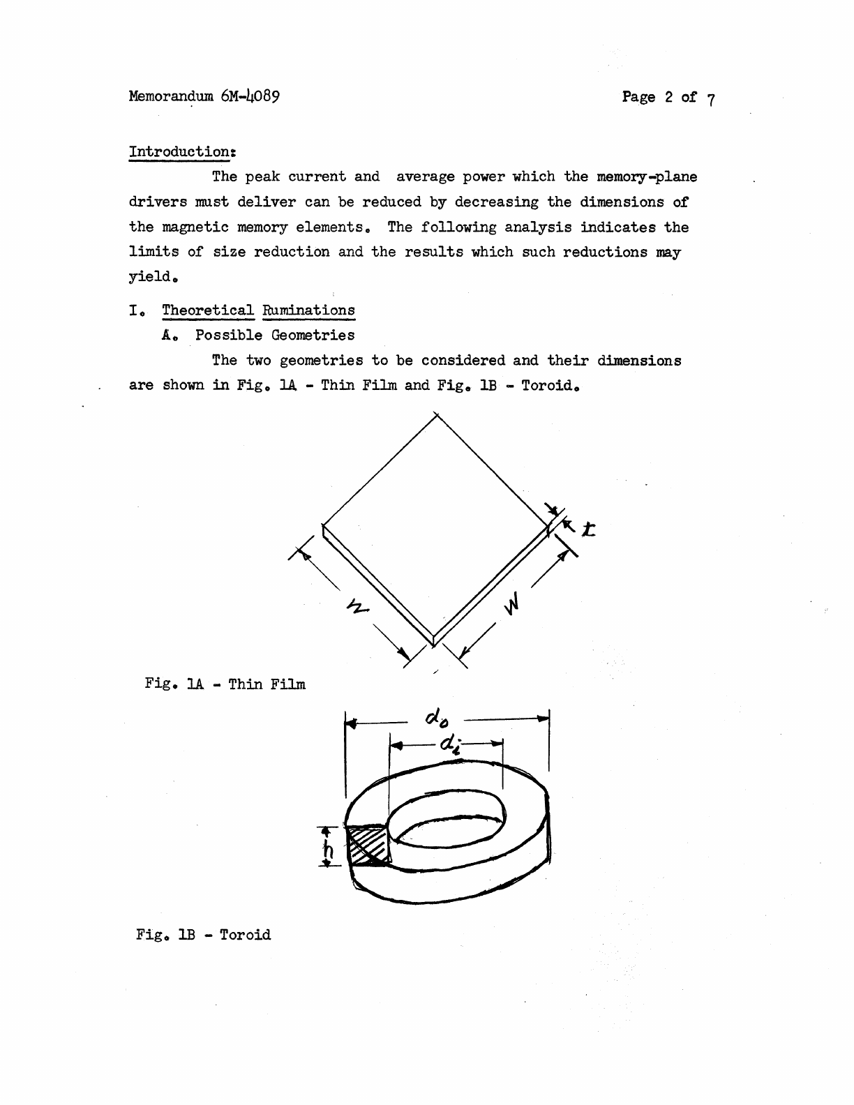
Ao
Possible
Geometries
The two
geometries
to
be
considered
and
their
dimensions
are
shown
in
Fig.
lA
-Thin
Film
and
Fig.
IB
-
Toroid.
Fig.
1A
-
Thin
Film
Fig.
IB
-
Toroid
Memorandum
6M-4089
Page 3
of
7
B 0 Primary
Limits
on
Geometry
The
primary
limits
on
geometry
are
(1)
the
peak
voltage
signal
V must be
great
enough
to
be sensed
reliably
and
(2)
the
p .
switch
time
~
must be
suitable
to
the
desired
memor,y
cycle
time
s
(certainly
less
than
half
the
cycle
time).
winding
is
Therefore
The
instantaneous
output
voltage
for
a one
turn
sense
-8
dB
v(
t)
=
10
A
Cit
•
where V
is
in
volts,~
in
seconds, A
in
square
centimeters,
and B
p s m
(the
maximum
induction
in
the
square
hysteresis
loop)
in
gauss.
We
can
express
the
requirement
on
A
in
terms
of
the
material
parameter
B
m
and
the
memor,y
limits
V and
~
as
p s
c.
Cross-Sectional
Areas
1.
Thin
Film
Let
w = C
1
t,
where Cl
is
a
constant
determined
by
the
magnitude
of
the
demagnetizing
field
tolerable
for
a square
loop;
C
l
is
in
the
order
of
1030
The
cross-sectional
area
is
thus
2
A =..!.
C
l
2.
Toroid
(I)
(2)
Because about
four
mutually
perpendicular
wires
of
a~sumed
diameter
d must
pass
through
the
toroidal
memory
element,
the
w
inner
diameter
d.
has
a lower
limit,
d.>
2d
;
also
geometry
dictates
that
1 I W
Memorandum
6M-4089
Page 4
of
7
the
following
assumptions be
made:
(a)
do = C2di; C2> 1
(b)
h = C
3di; C
3
/1
The
area
is
given
as
C
-1
2
k=C
3
Ld
41
2 i
Do
H-I
Relationships:
10 Thin
Film
In
the
calculation
of
the
field
between two
sheets
of
current,
the
following
approximations
are
made:
(a)
The
field
inside
a
rectangular
coil
of
length
w
centimeters
and
of
N
turns
is
the
same
as
for
a
similar
solenoid.
(3)
(b)
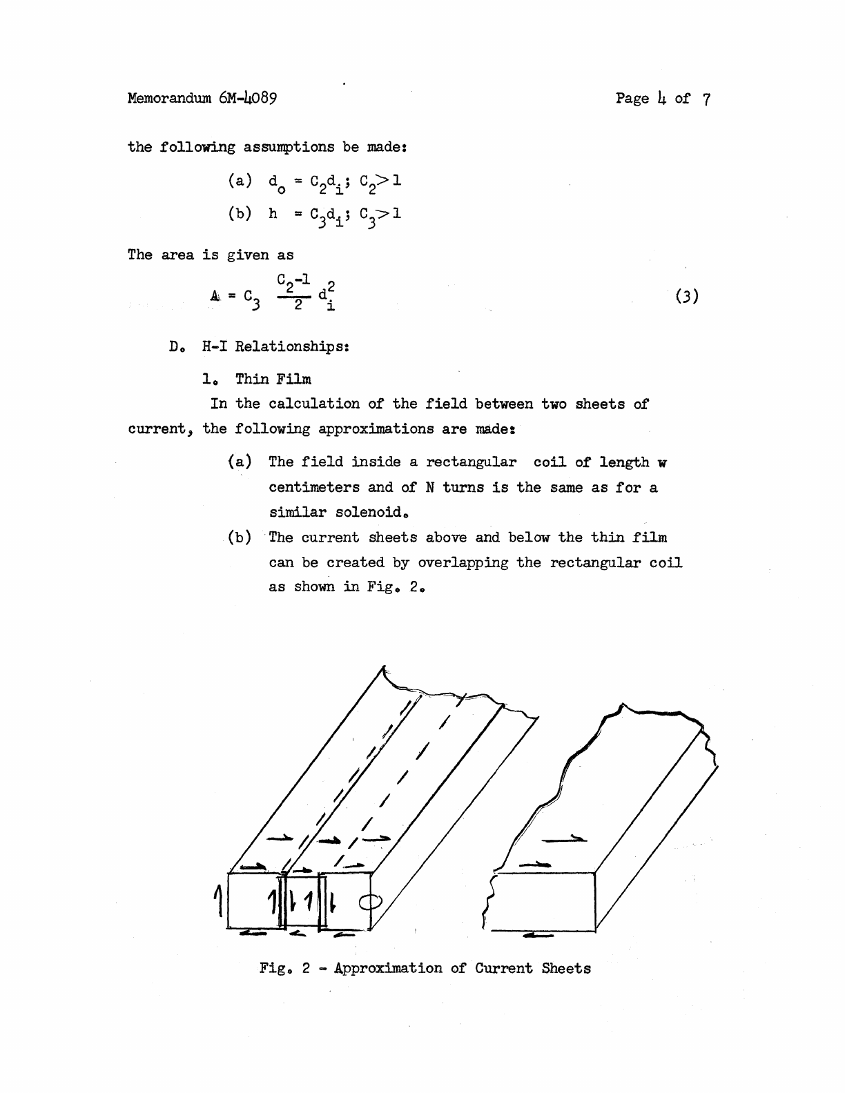
The
current
sheets
above and below
the
thin
film
can be
created
by
overlapping
the
rectangular
coil
as
shown
in
Fig.
20
Figo 2 - Approximation
of
Current
Sheets
Memorandum
6M-4089
Page 5
of
7
From
this
crude
analysis
we
get
4nN. 4 I
H
~
---2:. = n
law
lOw
(4)
where I
is
the
total
current
in
amperes
flowing
in
both
sheets
(split
equally
between
the
two) and H
is
in
oersteds.
2.
Toroid
The
field
in
a
toroid
is
H
~
8I
~
--IO---l(-d-+~d-
.....
)
o
~
E.
Geometry
Factor
We
define
a geometry
factor
F
as
g
H
F = - •
g I
(5)
(6)
SUbstituting
the
cross-sectional
area
limit
of
Eq.
(1)
into
Eqs.
(2)
and
(3)
and
these
into
Eqs.
(4)
and (5),
respectively,
gives
and
F
(thin
film)
~
8n
x
10-
51 v
Bm
\
g
'fCi
p't
s
F
(toroid)
g
F.
Order-of
-Magnitude
Calculations
For
purposes
of
comparison,
the
geometry
factor
of
the
F397
toroid
(d.=
54
mills,
d =
80
mills,
h =
22
mills)
is
2.4.
~
0
We
make
the
following
general
assumptions
for
both
geometries:
(1)
V
~
10-
2
volt
(in
present
memory
V
~
10-
1
volt)
p p
(2)
't
~
10-
7 second
(present
't
is
10-6
second).
s s
(8)

Memorandum 6M-4089 Page 6
of
7
With
these
assumptions,
we
get
for
thin
films
F
(thin
film)
~
16
oersted
g ampere
where 01= 2 x
10
3;
Bm=
8 x 10³
gauss,
typical
for
square
loop
metalso
For
a
toroid
where 02=
1;
03=
2;
Bm=
1~5
x.l0
3
gauss,
typical
for
ferrites,
. F
(toroid)
~
50
oersted
g ampere
The
next
section
indicates
the
relative
difficulty
of
obtaining
the
above
geometry
factors
o
IIo
Discussions
and
Conclusions:
The
ease
of
fabrication
is
one
factor
governing
the
practica:Lity
of
a
given
memory-element
geometry.
In
the
Fg
.factors
'.
.
-2,:1
..
;
above,
the
thin
film
would
have
the
dimensions
w =
7x
lO'em
by
t = 305 x
10
....
5 cm;
the
toroid,
d.
:;:::
3 x
10';"3
em, d = 6 x
lO-3
cm
, h =3xlO-3
cm
o
~
. 0
The
thin
film
could
be
made
by
evaporation
techniques
with
relative
ease;
but
the
ultra-small
toroid
would .be
almost·~
impossi'ble
to
make.
A
toroid
a
scale
magnitude
larger
would
be
possible;
this
gives
F
-:=.50
. g
Also
it
must
be
remembered
that
a miniDllm
of'
three
conductors
each
capable
of
carrying
milliampere
currents
must
pass
through
the
toroid
0
Thus
fabrication
difficulties
seem
to
make
the
thin
film
geometry
more
feasible
o
other
geometries
may
offer
mo~e
~han.the
thin
film
so
that
a
further
study
of
geometry
is
worthwhile.
Changing
geometry
alone
is
not
the
answer
to
the
very-fast-
memory.
problem.
In
the
preceding
calculations
it
has
been
assumed
that
magnetic
materials
and
memory scheme
exist
such
that
a memory
cycle
time
of
about
2 x 10 -7
second
is
possible
and
the
V
~
10-
2
volts
can
be
p
sensed
reliably.
In
conclusion,
a memory
element
can
be
reduoedin
size
(1)
yielding
an
improvement
in
the
peak
current-average
power
requirement
of
the
memory
(2)
at
the
expense
of
the
peak
signal
voltage
if
and
only
if
Memorandum
6M=4089
Page 7
of
7
(3)
a
material
and
memory scheme
exist
such
that
't'
~
10-
7
second
is
s
possible
e
JDC/md
