8.4.3a_Transient_Behavior_of_a_High_Speed_Tunnel Diode_Switching_Circuit_1963 8.4.3a Transient Behavior Of A High Speed Tunnel Diode Switching Circuit 1963
8.4.3a_Transient_Behavior_of_a_High_Speed_Tunnel-Diode_Switching_Circuit_1963 8.4.3a_Transient_Behavior_of_a_High_Speed_Tunnel-Diode_Switching_Circuit_1963
User Manual: 8.4.3a_Transient_Behavior_of_a_High_Speed_Tunnel-Diode_Switching_Circuit_1963
Open the PDF directly: View PDF ![]() .
.
Page Count: 12
-.
~-
-
'.'
•
'.,
<'
-~J'''''
:.~;..t>.~'
'.'
"t'
~-.
>.
~~.
.-.
~
~:
:~
• '
~.
•
'I~
'/t.
~:;;,
• _
~
..
~.,~
A
STUDY
OF
THE
TRANSIENT
BEHAVIOR
OF
A HIGH
SPEED
TUNNEL-DIODE
SWITCHING
CIRCUIT
USING AN ANALOG
COMPUTER
Section
I
II
III
by
GEORGE
HANNAUER
Electronic
Associates,
Inc.
TABLE
OF
CONTENTS
ANALYSIS
OF
SWITCHING
CIRCUIT
.................
.
THE
MATHEMATICAL
MODEL
....................
.
THE
COMPUTER
PROGRAM
......................
.
Page
2
4
5
A.
Solving
for
the
Derivatives
il
and
i2
. . . . . . . . . . . . .
..
5
B.
Generation
of
the
Characteristic
Curve
. . . . . . . . . . .
..
5
C.
Circuit
Diagram,
Figure
4
.....................
6
D.
Potentiometer
Sheet,
Figure
5 . . . . . . . . . . . . . . . . .
..
7
E.
Amplifier
Sheet,
Figure
6 . . . . . . . . . . . . . . . . . . . .
..
8
F.
Tables....
.
..............................
8
a.
Summary
of
Variables,
Table
2
...............
9
b.
Summary
of
Units
Used,
Table
3.
. . . . . . . . . . . .
..
9
c.
Summary
of
Parameter
Values.
Table
4.
. . . . . . .
..
9
G.
Static
Check
Calculations
......................
9
IV
RESULTS
AND
CONCLUSIONS.
. . . . . . . . . . . . . . . . . . .
..
10
V
REFERENCES.
. . . . . . . . . . . . . . . . . . . • . . . . . . . . .
..
12
Printe
d
in
U.
S.
A.
1
Bulletin
Number
ALAC-
6348
TABLE
OF
CONTENTS
Section
Page
I ANALYSIS
OF
SWITCHING
cmCUIT
.•.••••••••••••••
1
IT
THE
MATHEMATICAL
MODEL
..••••.•..•.•••••.••
3
ill
THE
COMPUTER
PROGRAM
••••••••••••••••••.••
3
A.
Solving
for
the
Derivatives
11
and
12
• • • . . • • • . • • • . • 3
B.
Generation
of
the
Characteristic
Curve
. • • • • • • • • • • • 4
C.
Circuit
Diagram,
Figure
4 • • • • • • • • • • • • • • • • • • • • 5
D.
Potentiometer
Sheet,
Figure
5.
• • • • • • • • • • • • • • • • • 6
E.
Amplifier
Sheet,
Figure
6.
• • • • • • • • • • • • • • • • • • • • 7
F. Tables
.................................
8
a.
Summary
of
Variables,
Table
2 • • • • • • • • • • • • • • 8
b.
Summary
of
Units
Used,
Table
3 • • • • • • • • • • • • • 8
c.
Summary
of
Parameter
Values,
Table
4 • • • • • • • • 8
G.
Static
Check
Calculations
•••
; • • • • • • • • • • • • • • • • • 8
IV
RESULTS
AND CONCLUSIONS
••••••••••••••••••••
9
V
REFERENCES
• • • • • • • • . . • • • . • • • . • • • • • • • • • • • • • 10
A STUDY OF THE TRANSIENT BEHAVIOR
OF
A HIGH
SPEED
TUNNEL-DIODE SWITCHING CIRCUIT USING AN ANALOG
COMPUTER
by
GEORGE HANNAUER
Electronic
Associates,
Inc.
I.
ANALYSIS
OF
SWITCHING CIRCUIT
The
switching
circuit
is
best
understood
by
refer-
ence
to
the
simplified
schematic
drawing
in
Fig-
ure
1.
The
voltages
V + and
V_are
bias
voltages
provided
by
an
external
source,
and
are
assumed
to
be
equal
in
magnitude
and
opposite
in
polarity.
The
tunnel
diodes
TD1 and TD2
are
identical.
If
no
inputs
or
loads
are
connected
to
the
circuit,
the
same
current
will
flow
through
both
diodes.
If
the
volt-ampere
curve
of
the
diodes
always
ex-
hibits
a
positive
resistance
characteristic,
the
voltage
drops
across
the
diodes
will
be
identical,
and
the
voltage
at
the
juncture
of
the
diodes
will
be
zero.
TDI
Vin
V out
~TD2---~
LOAD
V-
Figure
1.
Simplified
Schematic
for
Tunnel-Diode
Switching
Circuit
The
characteristic
curve
of
a
typical
tunnel
diode
is
given
in
Figure
2. Note
that
the
slope
is
nega-
tive
over
the
greater
portion
of
the
operating
range
(from
about
60
to
300
millivolts).
The
exist-
ence
of
this
negative
resistance
region
means
that
the
equilibrium
described
in
the
preceding
para-
graph
will
be
unstable.
A
very
slight
disturbance
will
upset
the
summetry
described
above,
causing
a
very
much
larger
voltage
to
appear
across
one
diode
than
across
the
other.
This
sensitivity
to
small
input
disturbances
enables
the
circuit
to
function
as
a
high-gain
high-speed
switch.
1
Assume
V + and
V_are
initially
zero
and
that
V +
gradually
increases
while
V_decreases,
such
that
V + + V _ =
O.
Then
the
operating
point
of
each
diode
will
move
from
the
origin
in
Figure
2
along
the
characteristic
curve
toward
the
peak.
The
volt-
age
at
the
junction
will
remain
zero,
as
before.
After
the
peak
has
been
passed,
the
voltages
and
currents
for
the
two
diodes
should
remain
identi-
cal
(by
symmetry),
and
the
voltage
at
the
junction
should
remain
zero.
However,
since
the
diodes
are
now
in
their
negative
resistance
region,
this
equilibrium
will
prove
extremely
unstable.
Suppose,
for
instance,
that
the
circuit
is
unbal-
anced
by
a
small
positive
voltage
at
the
input
terminal.
Then
tunnel
diode
#2
will
have
a
slightly
greater
voltage
across
it
than
tunnel
diode
#1,
and
as
the
bias
voltage
increases,
tunnel
diode
#2
will
pass
its
peak
first.
Further
increases
in
the
volt-
age
across
TD2
will
result
in
a
decrease
in
the
current
through
it,
and
hence
a
decrease
in
the
current
through
TD1
as
well.
Since
TDI
is
still
in
its
positive
resistance
region,
a
decrease
in
its
current
will
decrease
its
voltage
drop,
increas-
ing
the
voltage
drop
across
TD2
(since
the
tunnel
diodes
are
acting
as
a
voltage
divider,
and
the
sum
of
their
voltage
drops
must
equal
2V
+).
It
follows
that
TD2
will
move
rapidly
through
its
negative
resistance
region,
at
a
speed
limited
only
by
circuit
reactances,
and
stabilize
somewhere
in
the
positive
resistance
region
above
300
milli-
volts,
while
TDI
stabilizes
in
the
positive
re-
sistance
region
below
60
millivolts.
Since
most
of
the
voltage
drop
between
the
two
bias
sources
appears
across
TD2,
it
follows
that
the
voltage
at
the
junction
(the
output
voltage)
will
be
positive.
A
positive
input
voltage
will
therefore
produce
a
positive
output
voltage.
The
output
volt-
age
will
be
of
the
same
order
of
magnitude
as
the
bias
voltage
V
+,
while
the
input
voltage
need
only
be
large
enough
to
overcome
any
inherent
imbal-
ance
in
the
diode
characteristics.
The
input
volt-
age
can
thus
be
made
very
small,
and
the
gain
of
the
circuit
is
limited
only
by
the
closeness
of
the
match
between
diode
characteristics
and
between

.......
en
~
0
en
>
a..
~
10
«
50
IJJ
...J
...J
CD
...J
«
~
0:: 8
40
<t
>-
I-
:z
0::
W
IJJ
0::
I-
6 0::
30
:)
:)
0...
U
:2:
IJJ
0 0
u 4 0
20
5
r---I
~
...J
0
IJJ
....
Z
L--I
2 :z
10
:)
I-
0 0 0 50
100
150
200
250
300
350
400 450
500
Vo
= TUNNEL
DIODE
VOLTAGE (
MILLIVOLTS)
0
+1
+2
+3
+4
+5
+6
+7
+8
.
+9
+10
[VO/50]
t COMPUTER VARIABLE ( VOLTS)
Figure
2.
Tunnel-Diode
Characteristic
Curve
the
positive
and
negative
power
supplies.
If
the
input
and
output
voltages
are
equal
in
magnitude,
as
is
the
case
with
cascaded
logic
elements
of
similar
design,
high
gain
means
that
very
large
resistors
can
be
used,
resulting
in
very
large
fan-in
and
fan-out
figures.
In
high-speed
logic
and
arithmetic
circuits,
the
voltages
V +
and
V_will
be
out-of-phase
alternat-
ing
voltages
with
approximately
sinusoidal
wave-
shapes,
D-C
levels
will
be
superimposed
on
these
sinusoids
and,
in
most
applications,
this
bias
will
just
equal
the
amplitude
of
oscillation
assuring
that
the
bias
voltages
do
not
change
sign.
The
alternating
bias
voltages
will
then
serve
as
a
"clock,"
supplying
the
necessary
timing
signals
for
high-speed
arithmetic
and
logic.
An
output
can
be
obtained
only
during
that
part
of
the
bias
cycle
when
the
bias
voltage
is
large
enough
to
switch
one
of
the
diodes
into
its
negative
re-
sistance
region.
The
attractiveness
of
this
circuit
for
digital
ap-
plications
lies
in
the
fact
that
the
input
need
only
2
be
large
enough
to
unbalance
a
symmetric
circuit.
If
all
components
were
perfectly
matched,
the
slightest
input
disturbance
would
unbalance
the
circuit
in
the
proper
direction,
and
the
theoretical
gain
would
be
infinite.
In
practice,
the
gain
will
be
limited
by
component
tolerances.
An
estimate
of
the
gain
(or,
equivalently,
the
fan-in/fan-out
cap-
ability)
of
the
circuit
can
be
made
from
a
static
analysis
of
the
tunnel-diode
characteristic
and
a
knowledge
of
circuit
tolerances.
Such
an
analysis
has
been
made
by
Chow
(4)
who
predicted
large
gains
for
closely
matched
diodes.
The
above
analysis
is
essentially
static.
For
de-
sign
purposes,
a dynamiC
analysis,
which
takes
circuit
reactances
into
account,
is
necessary
for
at
least
two
reasons:
1. A knowledge
of
the
switching
time
is
neces-
sary
to
determine
the
maximum
clock
fre-
quency
(i.e.,
the
maximum
rate
of
informa-
tion
transfer)
at
which
the
system
can
be
operated.
2.
Since
the
circuit
contains
two
negative-re-
sistance
elements,
it
may
well
prOve
unstable.
Instead
of
the
switching
behavior
described
above,
the
system
may
break
into
oscillations.
Both
the
stability
and
the
switching
time
will
depend
primarily
on
the
inevitable
circuit
reactances.
Fig-
ure
3
shows
the
equivalent
circuit
for
the
system,
with
circuit
reactances
and
external
loading
taken
into
account.
The
prinCipal
reactances
involved
are
lead
inductance
and
case
inductance
(which
may
be
lumped
together)
and
diode
shunt
capacitance.
Pro-
vision
is
also
included
for
coupling
the
leads
to-
gether
with
mutual'inductance,
which
would
corre-
spond
to
dressing
the
power
supply
leads
close
together
during
construction.
A
moderate
amount
of
coupling
proves
to
have
a
beneficial
effect
on
switching
time
when
the
circuit
is
operated
at
high
frequencies.
Figure
3.
Equivalent
Circuit
Showing
Reactances
Experimentation
with
the
actual
circuit
is
possi-
ble,
but
extremely
difficult
due
to
the
high
fre-
quencies
inVOlved (the
range
of
clock
frequencies
to
be
investigated
is
from
100
to
1000
mc.).
The
basic
Simplicity
of
the
equivalent
circuit
makes
it
easy
to
write
equations
to
describe
the
system
and
thus
study
the
mathematical
model
(the
equa-
tions)
rather
than
the
system
itself,
II,
THE
MATHEMATICAL
MODEL
The
equations
describing
the
system
are
given
be-
low.
These
equations
are
straightforward
applica-
tions
of
Kirchoff's
laws
and
the
known
properties
of
resistors,
capaCitors,
and
inductors,
They
may
be
written
down
immediately
upon
inspection
of
Figure
3,
. .
VI
II
r
1+
L1
11- M
12
+ V D + V
out
(1)
1
• .
-V
2
12
r2
+L
212
-M
\+VD2-Vout
(2)
3
VI
=
-V
=
EDC-A
sin
wt
2 (3)
. 1
VD = - I
1 C1 C1 (4)
. 1
VD = - I
2 C2 C2 (5)
IC I
-I
1 1
Dl
(6)
IC = I
-I
2 2 D2 (7)
ID f(VD )
1 1
(8)
ID = f(VD )
2 2
(9)
V =
(I1-I2+Iin)RL
out
(10)
V.
-V
out
1.
In
In
R. (11)
In
Equations
1 and 2
are
Kirchoff
voltage
equations
for
the
two
major
loops,
Equation
3
is
simply
the
statement
that
the
bias
or
"clock"
voltages
are
out-of-phase
sinusoids
with
DC
levels
superim-
posed,
Equations
4
and
5
state
the
basic
volt-
ampere
relation
of
a
capacitor,
and
6
and
7
are
Kirchoff
current
equations,
Equations
8
and
9
state
the
characteristic
relation
between
voltage
and
current
in
the
tunnel
diodes
(see
Figure
2).
On
the
computer,
these
curves
will
be
represented
by
function
generators.
Equations
10
and
11
are,
of
course,
statements
of
Ohm's
Law.
Equation
11
was
omitted
for
the
purposes
of
this
simulation,
and
replaced
by
the
assumption
that
the
input
current
lin
was
constant,
Values
from
0.5
up
to
2.0
rna,
were
tried.
The
assumption
of
con-
stant
input
current
implies
a
constant-current
source,
which
is
not
very
realistic.
This
simpli-
fication
is
not
necessary,
and
equation
11
could
be
programmed
directly
by
adding
one
additional
sum-
mer
and
one
inverter
to
the
analog
circuit,
The
simplification
was
made
in
the
present
study
so
that
the
results
could
be
compared
directly
with
Herzog's
digital
solution
(Ref.
2),
since
Herzog
also
made
this
assumption.
III.
THE
COMPUTER
PROGRAM
A.
Solving
for
the
Derivatives
i1
and
i2
The
first
step
in
deriving
a
computer
program
is
to
solve
all
differential
equations
for
the
highest
derivatives.
This
has
already
been
done
in
equa-
tions
4 and 5,
but
equations
1 and 2
contain
the
derivatives
i1 and i2, and
each
~erivat~ve
appears
in
both
equations.
To
solve
for
11
and
12,
we
must
treat
these
as
a
simultaneous
system
of
two
equa-
tions
in
two unknowns.
This
system
maybe
solved
by
determinants,
but
the
resulting
computer
cir-
cuit
would
be
unnecessarily
complex.
A
far
simpler
approach
is
to
solve
equation
1
for
i1
and
equation
2
for
i2,
giving
• 1 •
I
=-(V-I
r+MI-V
-V
)
1 L 1 1 1 1 2 D
lout
(1 *)
1 •
i2 =
-(-V
-I
r
+MI·-V
+V )
L2 2 2 2 1 D2
out
(2*)
These
equations
give
i1
in
terms
of
i2 and
vice
versa.
Programming
them
directly
leads
to
an
algebraic
loop (a loop
with
no
integrators),
and
since
this
is
a
two-amplifier
loop,
positive
feed-
back
is
present.
For
stability,
we
must
have
a
loop
gain
of
less
than
one
(Ref 5).
By
inspection
of
the
circuit,
it
is
easily
seen
that
the
loop
gain
is
M2
/L1
1,2' Since
this
is
always
less
than
one
on
physical
grou~ds,
t~e
loop
is
stable
and
the
correct
values
of
11
and
12
may
be
obtained
without
determinants
(Reference
6).
B.
Generating
the
Characteristic
Curve
The
tunnel-diode
characteristic
in
Figure
2
pre-
sents
a
problem
in
function
generation
no
matter
which
simulation
method
is
used.
On
adigitalcom-
puter,
the
function
values
can
be
stored
in
main
memory
in
tabular
form,
perhaps
with
an
inter-
polation
subroutine
to
fill
in
the
gaps
between
tab-
ulated
values.
If
enough
values
and/or
a
sufficiently
sophisticated
interpolation
scheme
are
stored,
a
tremendous
demand
is
made
upon
the
memory,
If
the
digital
computer
is
not
called
upon
to
solve
the
dynamic
equations
as
well,
this
is
an
acceptable
technique.
This
was
the
approach
used
by
Axelrod
(3).
The
simulation
was
essentially
analog,
with
the
digital
cOP.juter
serving
only
as
11
function
gener-
ator.
Herzog
(4)
uses
a
digital
computer
for
the
entire
problem.
The
characteristic
curve
is
represented
by
an
analytic
expression
of
four
terms
involving
a
polynomial,
two
exponential
functions
and
afrac-
4
t:ional
power.
This
expression,
which
was
obtained
.
from
a
separate
digital
computer
run
by
curve-
fitting,
can
be
programmed
with
standard
sub-
routines.
On
an
analog
computer,
the
best
approach
is
straightforward
use
of
a
standard
function
genera-
tor.
The
diode
function
generator
(DFG)
uses
biased
diode
networks
to
approximate
a
curve
by
straight-
line
segments.
On
the
TR-48
variable-breakpoint
DFG,
eleven
segments
are
available.
The
break-
points
(corners)
of
the
curve
may
be
varied
so
as
to
group
many
short
straight-line
segments
to-
gether
where
the
graph
curves
most
sharply
and
use
fewer
segments
where
the
graph
is
straighter.
In
this
way,
an
over-all
accuracy
of
about
1%
is
maintained
for
this
particular
curve.
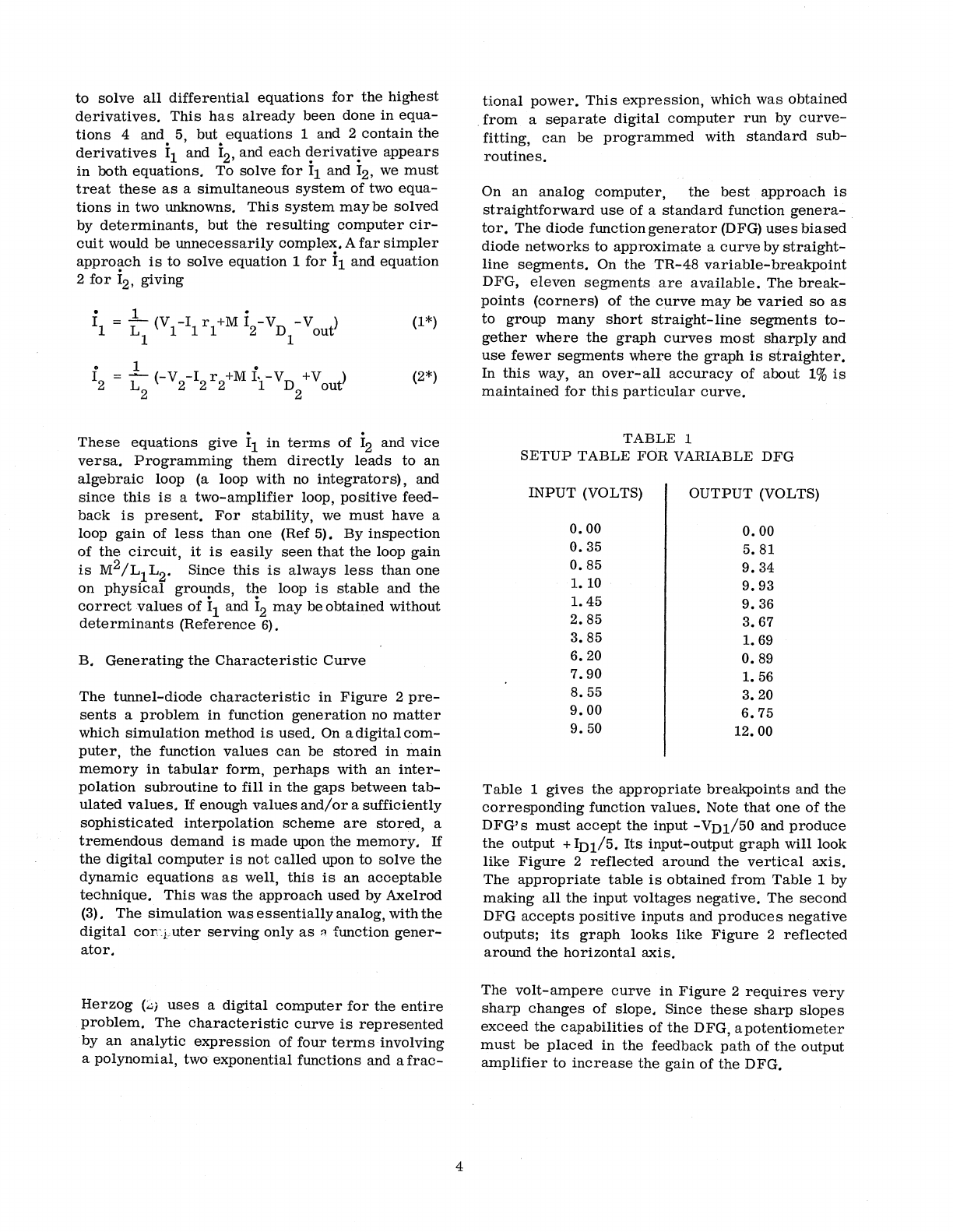
TABLE
1
SETUP
TABLE
FOR
VARIABLE
DFG
INPUT (VOLTS)
OUTPUT
(VOLTS)
0.00 0.00
0.35
5.81
0.85
9.34
1.
10
9.93
1. 45
9.36
2.85
3.67
3.85
1.
69
6.20
0.89
7.90
1.56
8.55
3.20
9.00
6.75
9.50
12.00
Table
1
gives
the
appropriate
breakpoints
and
the
corresponding
function
values.
Note
that
one
of
the
DFG's
must
accept
the
input
-VDl/50
and
produce
the
output
+
ID1/5.
Its
input-output
graph
will
look
like
Figure
2
reflected
around
the
vertical
axis.
The
appropriate
table
is
obtained
from
Table
1
by
making
all
the
input
voltages
negative.
The
second
DFG
accepts
positive
inputs
and
produces
negative
outputs;
its
graph
looks
like
Figure
2
reflected
around
the
horizontal
axis.
The
volt-ampere
curve
in
Figure
2
requires
very
sharp
changes
of
slope.
Since
these
sharp
slopes
exceed
the
capabilities
of
the
DFG,
apotentiometer
must
be
placed
in
the
feedback
path
of
the
output
amplifier
to
increase
the
gain
of
the
DFG.
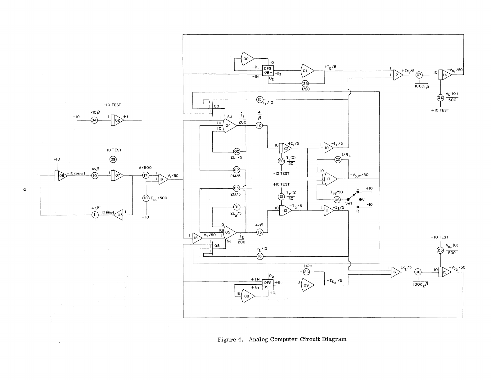
-10
TEST
~
/10/3
-10
I
+1
04
02
-10
TEST
")---.------110
;r----'----/
II
r2/10
L-~------------~16~------------------------~
Figure
4.
Analog Computer
Circuit
Diagram
L
+10
---
eC
~
R
I
100C I
/3
I
IOOC
2
/3
+10
TEST
-10
TEST
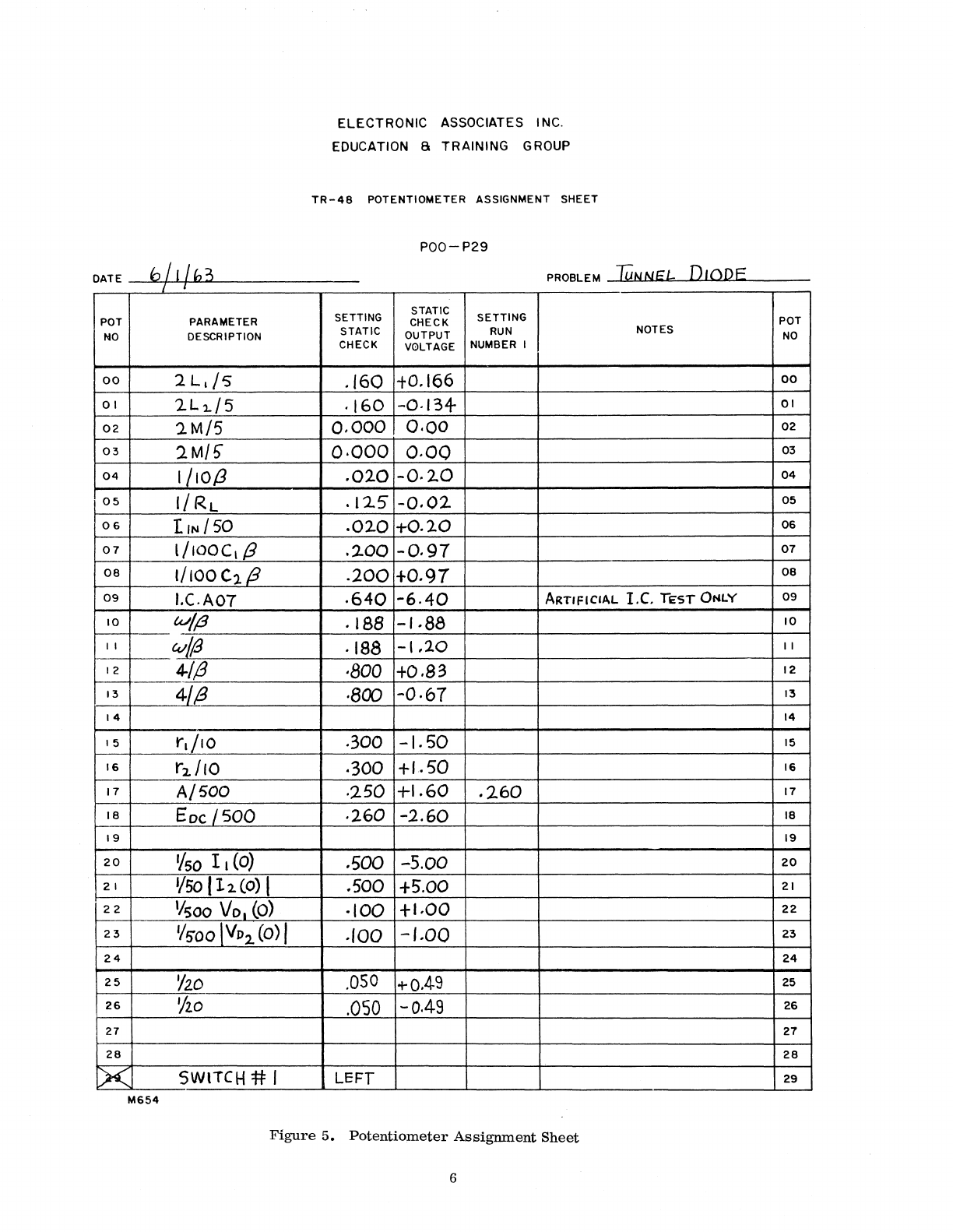
ELECTRONIC
ASSOCIATES INC.
EDUCATION a
TRAINING
GROUP
TR-48
POTENTIOMETER ASSIGNMENT SHEET
POO-
P29
DATE
b/llfn~
PROBLEM
Tu~N5:l=
DIQQE
SETTING
STATIC
SETTING
POT
PARAMETER
CHECK
POT
NO
DESCRIPTION STATIC OUTPUT
RUN
NOTES
NO
CHECK
V0LTAGE
NUMBER
I
00
2
L,
/5
.160
+0.166
00
01
2L·L/5
·160
-0.134-
01
02
'l
M/5
0.000
0·00
02
03
2M/5"
0·000
0.00
03
04
I/IO{J
.020
-0·
20
04
05
1/
RL
.125
-0.02
05
06
I
IN
/50
.020
+0.20
06
07
I/IOOC,
B
.200
-0.97
07
08
1/100
Cl
(3
.200
+0.97
08
09
I.('A07
.640
-6.40
ARTIFICIAL
I.e.
TEST
ONI.Y
09
10
W/f3
.188
-1·88
10
-
f-.-
-
I I
w/(3
·188
-1,20
II
12
___
4-1/3
·800
+0.83
12
--
13
~
·800
-0·67
13
14
14
15
rl/IO
.300
-1.50
15
16
rl.
/10
·300
+1.50
16
17
A/500
·250
+1.60
,260
17
18
Eoc
/500
·260
-2.60
18
19
19
20
1/50
I
1(0)
.500
-5.00
20
21
I/SO
Ill.
(0) I
.500
+5.00
21
22
Iisoo
VOl
(0)
·100
t1.00
22
r-
I/
SOO
IVp2.
(0) I
23
.100
-/.00
23
24
24
25
'Izo
.050 +0.49
25
26
'/lO
.050
-0.49
26
27
27
28 28
l><
SWITCH # I LEFT
29
M654
Figure
5.
Potentiometer
Assignment
Sheet
6
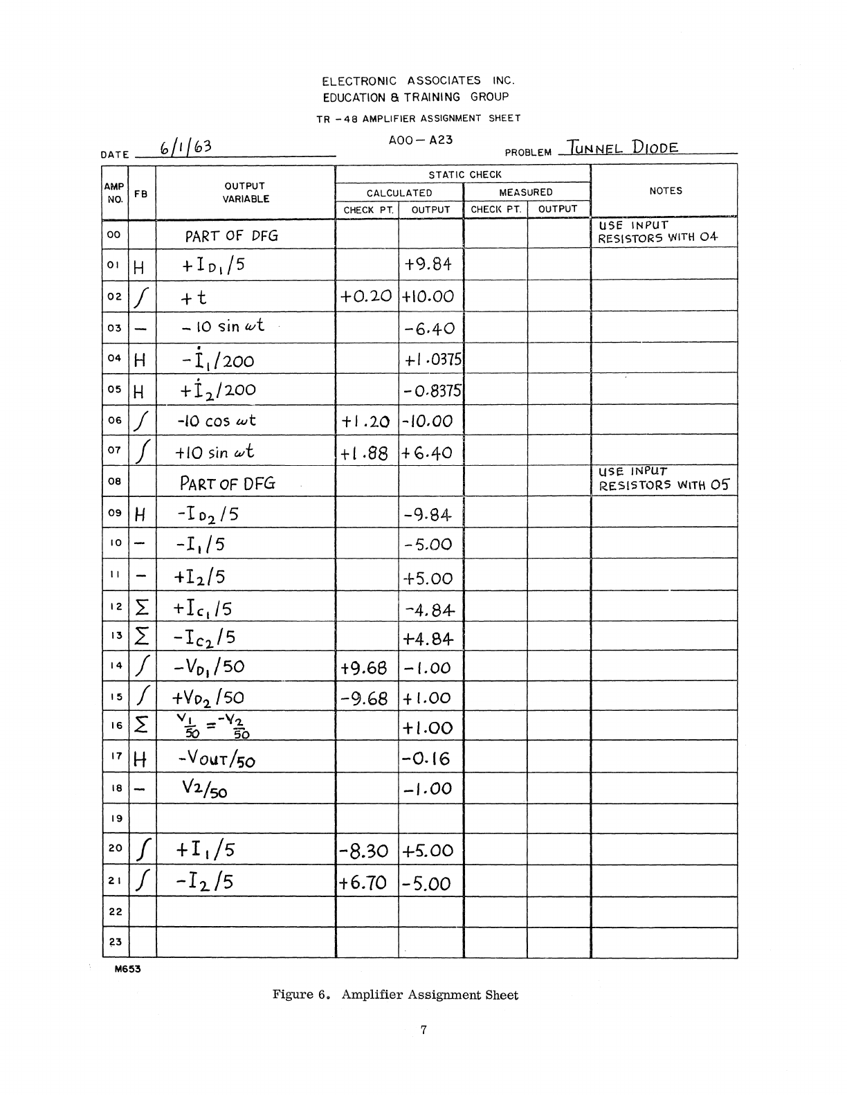
ELECTRONIC ASSOCIATES INC.
EDUCATION
a TRAINING
GROUP
TR
-48
AMPLIFIER ASSIGNMENT SHEET
DATE
_--=b...L..I---,'
IL-0_3
_____
_
AOO-
A23
PROBLEM
_TlJ..!Uo.!.!N~N!.:!..IE=...!-
L~D~I~Q~D..!:::E'__
__
STATIC
CHECK
AMP
OUTPUT CALCUl.ATED MEASURED NOTES
NO.
FB VARIABLE
CHECK
PT.
OUTPUT
CHECI(
PT. OUTPUT
00
PART
OF
DFG
USE
INPUT
REOSISTOR5
WITH
04-
01 H
+ID,/5
t9.84
02
I
+t
+0.20
+10.00
03
--
10
sin
wt
-6.40
.
04
H - 11
/200
+1
·0375
05
H +
12./
200
-0.8375
06
J -10 cos
wt
tl.20
-10.00
07
j
tlO
sin
wt
+1.88
+6·40
PART
OF
DFG
use
INPUT
08
RESISTORS
WITH
OJ
09
H -I
Dl
/5
-g.84-
10 -
-Ills
-5.00
II
-
+Il/S
+5.00
12
2:
+ Iel/S
-4.84-
13 I
-Ic2.
/5
+4.84-
14 /
-V
DI
/50
+9.68
-1.00
.
15 f
+V0
2 Iso
-9.68
+1.00
16 2
VJ..
_-'1'1
50-
50
+1.00
17
H -VOUT/SO
-0.16
18
-
V2/
SO
-1.00
19
20
f
+II/S
-8.30
+5.00
21
I
-I2/5
t6.10
-5.00
22
23
M653
Figure
6.
Amplifier
Assignment
Sheet
7
TABLE
2
SUMMARY
OF
VARIABLES
Original
Variable
Max
Value
500
mv
50
rna
50
rna
2000
mains
50
rna
Scale
factor
1
Volt/mv
50
1
Volt/rna
5
1
Volt/rna
5
1
Volt/mains
200
1
Volt/rna
5
:
Scaled
Variable
J~
V]
l50
Tl
I ]
l5
D
~~
I]
iJ
~Il
rJ
:l?
C
.
[1
;L200
{3
5
seconds
machine
time
1
nanosecond
problem
time
TABLE
3. SUMMARY
OF
UNITS
OF
MEASUREMENT USED
Voltage:
millivolts
Current:
milliamps
Resistance:
ohms
Inductance:
nanohenries
(10-
9
henry)
Capacitance:
nanofarads
(10-
9
farad)
Time:
nanoseconds
(10-9
sec)
Note:
The
use
of
the
somewhat
unusual
units
for
inductance
and
capf!-citance
gu~rantees
that
the
equations
I = CV and V =
LI
will
hold
in
this
system
of
units.
G.
Sun1mary
of
Static
Check
Conditions
For
static
check
calculations,
convenient
values
are
selected
for
all
integrator
output
signals
(in
this
case
II,
12,
VDl'
and VD2) and
for
the
driving
func-
tions,
VI,
V2, and
lin'
These
values
may
be
chosen
arbitrarily,
but
they
should
be
small
enough
to
avoid
amplifier
overloads
and
large
enough
to
pro-
vide
amplifier
output
signals
that
can
be
measured
with
reasonable
accuracy.
The
values
cho
sen
were:
II
=
+25
rna.
12
=
+25
rna.
VDl
=
+50
mv.
VD2 =
+50
mv.
M
I.
In
A
Edc
f
w
8
TABLE
4
SUMMARY
OF
PARAMETERS
r2 = 3
ohms
8
ohms
C2
10-
2
nanofarads
L2 =
0.4
nanohenry
~v'LT
1 2
1.
0 mao
Try
M = 0
for
first
run.
Prob-
able
maximum
value
around
O.
2
nanohenry.
130
millivolts
130
millivolts
150
megacycles/second
=
0.15
cycles/na-
nosecond
27rf =
0.9425
radians/no
S.
VI
= +50
mv.
lin
= + 1.0 mao
Parameter
values
are
the
same
as
those
for
the
first
run.
The
values
for
all
variables
may
be
cal-
culated
from
equations
1 - 10.
These
values
are
given
below.
ID1 =
+49.2
mao ID2 =
+49.2
mao
IC1 =
-24.2
mao
V
out
=
+8
mv.
IC2 =
-24.2
mao
The
derivatives
may
be
calculated
from
equations
1 *, 2*, 4, and 5.
These
are:
"D1
= V
D2
=
-2420
millivolts/nanosecond
.
II
=
-207.50
milliamps/nanosecond
.
12
=
-167.50
milliamps/nanosecond.
All
variables
that
have
been
calculated
can
now be
translated
into
amplifier
output
voltages.
These
voltages
appear
on
the
amplifier
assignment
sheet.
They
may
be
checked
against
values
calculated
on
the
circuit
diagram
(to
check
the
programming
and
scaling)
and
later
checked
against
actual
measured
voltages
on
the
computer
(to
check
the
patching
and
the
functioning
of
the
components).
The
check-
points
should
also
be
calculated
and
measured
for
integrators.
(The
checkpoint
of
an
integrator
is
minus
the
sum
of
its
input
voltages.
It
may
be
read
out
by
patching
the
summing
junction
of
the
inte-
grator
temporarily
to
the
summing
junction
of
a
summing
amplifier
that
is
not
being
used
in
the
problem).
These
calculated
values
are
also
tabu-
lated
in
the
amplifier
assignment
sheet.
The
initial
condition
voltages
marked
"Test"
are
for
static
test
purposes
only, and
not
forthe
actual
run.
They
should
be
removed
prior
to
the
first
run.
Note
that
the
static
test
value
of
the
mutual
ind1lct-
ance
M
is
zero.
This
value
was
chosen
to
break
the
algebraic
loop
in
the
static
test
mode,
since
otherwise
it
would
be
very
hard
to
troubleshoot.
However,
this
static
test
value
does
not
check
the
algebraic
loop
itself,
and a
supplementary
test
should
be
included
with
M
f.
O.
For
this
supple-
mentary
test,
we
may
as
well
assume
that
the
arti-
ficial
initial
conditions
on
voltages
and
currents
are
zero,
since
this
part
of
the
circuit
has
already
been
checked
by
the
main
static
check.
Eqaations
1
and
2
then
become:
9
VI
= L1 i1 -Mi2
-V2
= L2i2
-Mil
Solving
by
determinants:
• V1L2
-MV
2
-L
V
+MV
1 2 1
II
= 2
L1L2
-M
L L _M2
1 2
If
we
let
VI
= 50
mv,
V2 =
-50
mv,
Ll
= h
=.0.4
nanohenry
and M = 0.2
nanohenry,
then
II
=
12
+ 250.0
milliamps/nanosecond.
The
output
of
amplifier
04
should
be
-il
/200
=
-1.25
volts,
and
the
output
of
amplifier
05
should
be
+
1.25
volts.
IV. RESULTS
AND
CONCLUSIONS
The
switching
transients
and
output
wave
shape
s
for
constant
input
current
are
shown
ih
Figures
7
and
8. Note
in
particular
that
at
300
megacycles
the
output
voltage
goes
through
an
initial
oscillation
be-
fore
switching.
The
output
is
high
for
only
a
short
period
of
time
late
in
the
bias
cycle.
At
150
mega-
cycles,
the
output
rises
much
more
sharply
and
gives
a good
waveshape.
200
f:z
150mc
100
BIAS
VOLTAGE_
2 3 4 5 6 7
time
-
nanoseconds
Figure
7. Output Wave
shape
of
Switching
Circuit
at
150
Megacycle
Clock
Frequency
200
100
2 3 4 6 7
time
-
nanoseconds
Figure
8. Output Wave
shape
at
300
Megacycle
Clock
Frequency
B
B

Operation
at
300
megacycles
is
possible,
but
margi-
nal.
Further
experimentation
with
the
model
indi-
cates
that
for
reliable
operation
with
sufficiently
large
fan
in/fan
out
capability
the
circuit
should
not
be
operated
above
about
200
or
250
megacycles.
It
is
significant
that
a
preliminarypencil-and-paper
analysis
indicated
that
the
system
ought
to
operate
at
frequencies
up
to
1000
megacycles.
A
circuit
designed
to
operate
at
this
frequency
would
not
func-
tion
properly
and would
be
extremely
hard
to
troubleshoot,
due
to
the
circuit
loading
of
the
mea-
suring
devices.
The
computer
solution
facilitates
fundamental
understanding
of
the
nature
of
the
switching
process,
as
well
as
providing
actual
so-
lutions.
The
ease
of
parameter
changing
on
the
analog
computer
makes
it
especially
easy
to
in-
vestigate
the
trade-off
between
gain
(Le.
fan
in/fan
out
capability)
and
frequency.
The
results
agree
quite
well
with
Herzog's
digital
simulation,
using
the
Edsac
II
computer
at
Cam-
bridge
University,
and
for
further
analysis
of
the
results,
the
reader
is
referred
to
Herzog's
paper
(2).
It
is
instructive
to
compare
the
two
simula-
tions
from
the
point
of
view
of
flexibility
and
con-
venience.
a,
The
digital
program
requires
the
equations
to
be
written
as
a
set
of
first-order
equations,
solved
for
the
highest
derivatives,
and
t11en
converted
into
algebraic
equations
by
the
Runge-Kutta
or
a'simi-
lar
integration
scheme.
While
standard
software
is
available
in
many
installations
to
simplify
this
task,
it
is
completely
eliminated
in
an
analog
sim-
ilation,
since
the
analog
solves
differential
equa-
tions
~
differential
equations,
b.
The
running
time
for
the
Edsac
II
was,
accord-
ing
to
Herzog,
about
three
minutes
per
solution,
as
opposed
to
25
seconds
on
the
TR-48
computer
--
a
speed
advantage
of
seven
to
one.
Nothingprecludes
running
even
faster
than
this,
since
the
components
are
operating
well
within
their
frequency-response
limitations.
The
solution
also
can
be
run
in
repeti-
tive
operation,
in
which
case
the
solution
takes
only
50
milliseconds
--
effectively
zero
solution
time
as
far
as
the
operator
is
concerned.
c.
Even
more
important
than
running
time
per
se
is
the
time
required
to
obtain
meaningful
and
useful
results.
The
output
of
the
analog
unit
is
a
continuous
graph,
drawn
in
ink
on 11 x
17"
paper
...
a
form
of
output
which
an
engineer
can
readily
observe
and
interpret.
By
contrast,
the
digital
results
were
ob-
tained
from
an
on-line
printer,
and
considerable
manual
effort
was
required
to
translate
these
re-
sults
into
graphical
form.
Of
course,
on-line
devices
are
available
for
pro-
ducing
graphical
readout
from
a
digital
computer.
Some
of
Herzog's
graphical
results
were
obtained
by
oscilloscope
photography.
Although
this
method
eliminates
the
tedium
of
point-plotting,
it
ismessy
and
time-consuming,
and
offers
limited
resolution.
Perhaps
the
best
form
of
readout
(certainly
the
most
convenient)
involves
the
use
of
a
digital-to-
analog
converter
and
an
analog
X-
Y
plotter.
While
this
method
is
acceptable,
it
requires
expensive
conversion
eqUipment
to
translate
the
data
into
analog
voltages
for
plotting.
Such
conversion
equip-
ment
is
unnecessary
with
the
TR-48
computer
since
the
signal
is
an
analog
voltage
in
the
first
place.
d.
Since
only
about
half
of
the
computing
capacity
of
the
TR-48
computer
is
used,
the
simulation
can
easily
be
expanded
to
take
additional
effects
into
account.
Herzog's
equations
assumed
a
constant
current
input
and
ignored
the
fact
that
the
load
is
not
purely
resistive.
These
simplifications
could
easily
be
removed
on
an
analog
simulation
by
addition
of
a
few
more
amplifiers
and
potentio-
meters.
On a
digital
computer,
any
additional
complexity
in
the
equations
would
increase
the
running
time.
An
attractive
alternative,
for
example,
would
be
to
simulate
an
additional
tunnel-diode
circuit
on
the
analog
computer
and
feed
the
output
of
the
first
into
the
second.
This
would
enable
the
designer
to
determine
how
flat
the
output
wave
shape
of
the
first
cirCuit
would
have
to
be
in
order
to
trigger
the
second
successfully.
V.
REFERENCES
r
1.
Gibson,
J.J.
"An
Analysis
of
the
Effects
of
Reactances
on
the
Performance
of
the
Tunnel-Diode
Bal-
anced
Pair
Logic
Circuit"
RCA
Review,
December,
1962,
p.
457.
~'o.~~rzog,
G.B.
"Tunnel-Diode
Balanced
Pair
Switching
Analysis"
RCA
Review,
June,
1962,
Vol. XXIII,
3.
Axelrod,
Barber
and
Rosenheim
"&>me
New
High-Speed
Tunnel-diode
Logic
Circuits"
mM
Journal
April,
1962.
'
4.
Chow,
W.F.
"TWillel-Diode
Digital
Circuits"
IRE
Transactions
on
Electronic
Computers
Vol
EC
9
September,
1960,
page
295.
' • ,
5.
Rogers,
A.E.
and
T.W.
Connolly,
"Analog
Computation
in
Engineering
Design"
McGraw-Hill
1960
Chapter
6, ' ,
6.
Hannauer,
G.,
"Algebraic
Loops",
E&T
Memo
#22,
Electronic
ASSOCiates,
Inc.,
P.O.
Box
582,
Prince-
ton,
N.J,
10
ELECTRONIC
ASSOCIATES, INC. Long Branch,
New
Jersey
ADVANCED
SYSTEMS
ANALYSIS
AND COMPUTATION SERVICES/ANALOG
COMPUTERS/HYBRID
ANALOG-DIGITAL COMPUTATION EQUIPMENT/SIMULATION SYSTEMS/
SCIENTIFIC
AND
LABORATORY
INSTRUMENTS/INDUSTRIAL
PROCESS
CONTROl SYSTEMS/PHOTOGRAMMETRIC EQUIPMENT/RANGE INSTRUMENTATION
SYSTEMS/TEST
AND CHECK-OUT
SYSTEMS/MILITARY
AND
INDUSTRIAL
RESEARCH
AND DEVElOPMENT
SERVICES/FIELD
ENGINEERING AND
EQUIPMENT
MAINTENANCE
SERVICES.
