89758600A_AT310 A_TTL_A_Q DSA_Bus_Expander_CE_Jul76 89758600A AT310 A TTL Q DSA Bus Expander CE Jul76
89758600A_AT310-A_TTL_A_Q-DSA_Bus_Expander_CE_Jul76 89758600A_AT310-A_TTL_A_Q-DSA_Bus_Expander_CE_Jul76
User Manual: 89758600A_AT310-A_TTL_A_Q-DSA_Bus_Expander_CE_Jul76
Open the PDF directly: View PDF ![]() .
.
Page Count: 62
89758600
CONTR..OL
DATA
CORPORATION
CONTROL
DATA®
TTL
A/Q-DSA
BUS
EXPANDER
AT310-A
GENERAL
DESCRIPTION
OPERATION
AND
PROGRAMMING
INSTAllATION
AND
CHECKOUT
THEORY
OF
OPERATION
DIAGRAMS
MAINTENANCE
PARTS
DATA
WIRE
LISTS
MAINTENANCE
AIDS
HARDWARE
REFERENCE/
CUSTOMER
ENGINEERING
MANUAL
REVISION
RECORD
REVISION
DESCRIPTION
01
Released
to
Class
B,
15
November
1974
ECO
CKI026
A Released
to
Class A
bv
ECO
CK1535.
dated 1
July
1976
Publication
No,
89758600
©
1974.
1975.
1976
by
Control
Data
Corporation
Printed
in
the
United
States
of
America
ii
Address
comments
concerning
this
manual
to:
Control
Data
Corporation
Small
Computer
Development
Division
4455
Eastgate
Mall
La
Jolla,
California
92037
or
use
Comment
Sheet
in
the
back
of
this
manual.
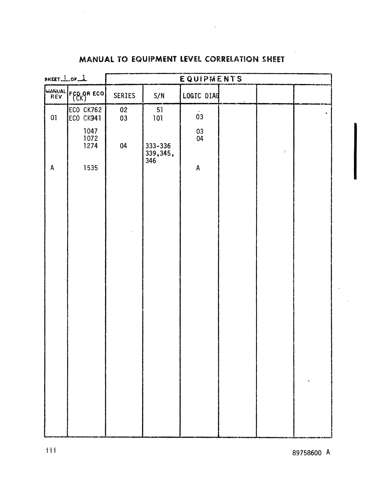
MANUAL
TO EQUIPMENT
LEVEL
CORREI.ATIOf"
SHEET
--
SNUT_
I
0'-1.
EQUiPMENTS
--~----
~At\IlIAl
FfeK~R
ECO
.
SERIES
SIN
LOGIC
DIA(
REV
ECO
CK762
02
51
01
ECO
CK941
03
101
03
1047
03
1072
04
1274
04
333-336
339,345, :
346
A
1535
A
.
--
iii
89758600
A

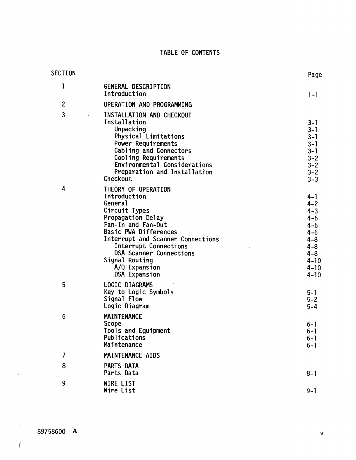
TABLE
OF
CONTENTS
SECTION
Page
1
GENERAL
DESCRIPTION
Introduction
1-1
2
OPERATION
AND
PROGRAMMING
3
INSTALLATION
AND
CHECKOUT
Installation
3-1
Unpacking
3-1
Physical Limitations
3-1
Power
Requirements
3-1
Cabling
and
Connectors
3-1
Cooling
Requirements
3-2
Environmental
Considerations 3-2
Preparation
and
Installation 3-2
Checkout
3-3
4
THEORY
OF
OPERATION
Introduction
4-1
General
4-2
Circuit
Types
4-3
Propagation
Delay
4-6
Fan-In
and
Fan-Out
4-6
Basic
PWA
Differences 4-6
Interrupt
and
Scanner
Connections
4-8
Interrupt
Connections
4-8
DSA
Scanner
Connections
4-8
Signal
Routing
4-10
A/Q
Expansion
4-10
DSA
Expansion
4-10
5
LOGIC
DIAGRAMS
Key
to
Logic
Symbols
5-1
Signal
Flow
5-2
Logic
Diagram
5-4
6
MAINTENANCE
Scope
6-1
Tools
and
Equipment
6-1
Publications
6-1
Maintenance
6-1
7
MAINTENANCE
AIDS
8
PARTS
DATA
Parts
Data
8-1
9
WIRE
LIST
Wire
Li
st
9-1
89758600
A v
(
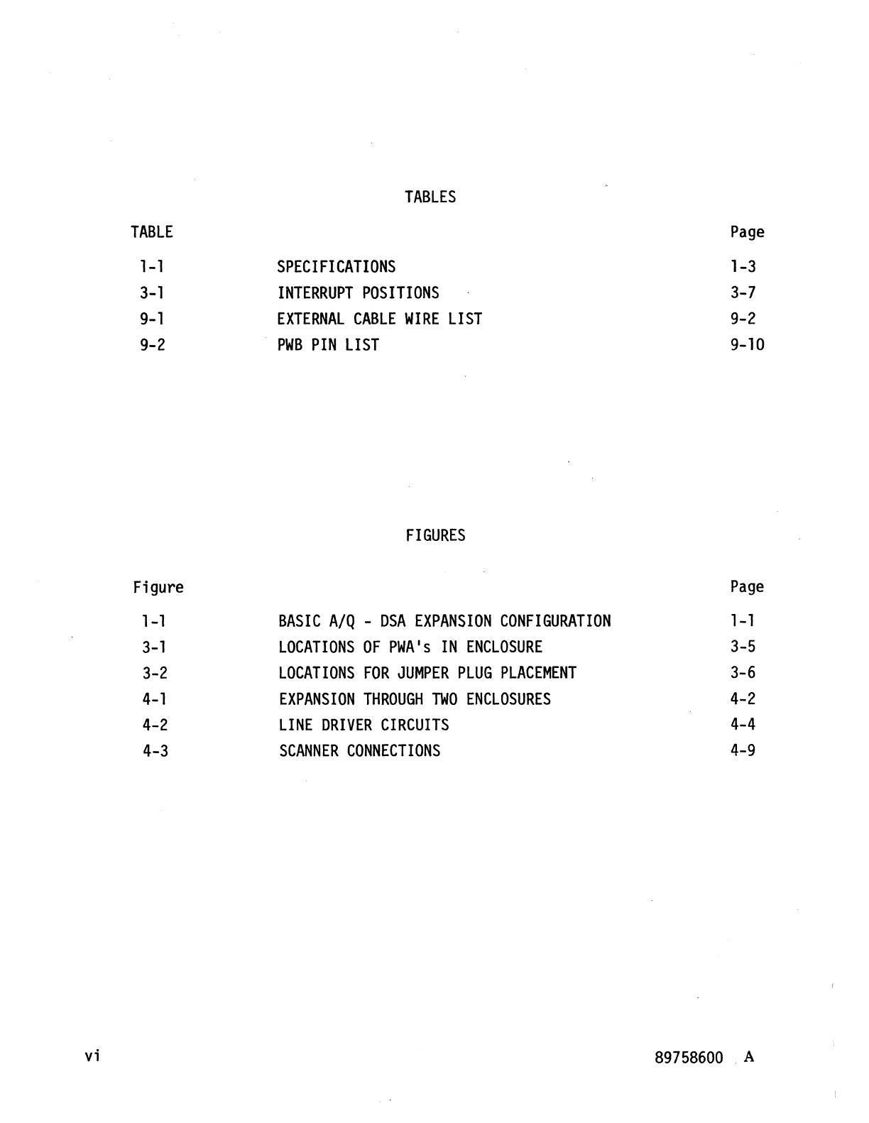
TABLES
TABLE
Page
1-1
SPECIFICATIONS
1-3
3-1
INTERRUPT
POSITIONS
3-7
9-1
EXTERNAL
CABLE
WIRE
LIST
9-2
9-2
PWB
PIN
LIST
9-10
FIGURES
Figure
Page
1-1
BASIC
A/Q
-
DSA
EXPANSION
CONFIGURATION
1-1
3-1
LOCATIONS
OF
PWA's
IN
ENCLOSURE
3-5
3-2
LOCATIONS
FOR
JUMPER
PLUG
PLACEMENT
3-6
4-1
EXPANSION
THROUGH
TWO
ENCLOSURES
4-2
4-2
LINE
DRIVER
CIRCUITS
4-4
4-3
SCANNER
CONNECTIONS
4-9
vi
89758600
. A
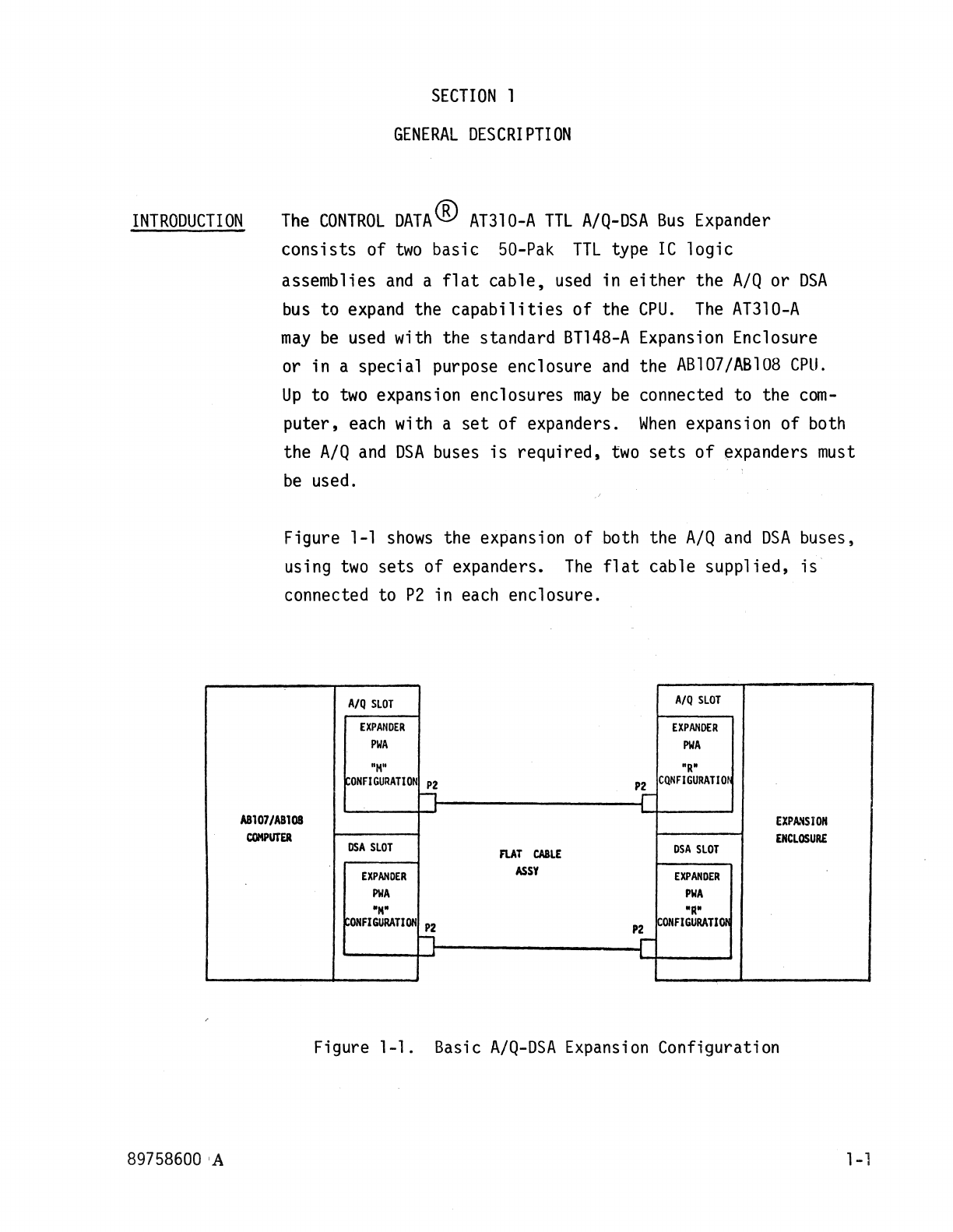
INTRODUCTION
SECTION
1
GENERAL
DESCRIPTION
The
CONTROL
DATA(8)
AT310-A
TTL
A/Q-DSA
Bus
Expander
consists of
two
basic
50-Pak
TTL
type
IC
logic
assemblies
and
a
flat
cable,
used
in
either
the
A/Q
or
DSA
bus
to
expand
the
capabilities
of
the
CPU.
The
AT310-A
may
be
used
with the standard
BT148-A
Expansion
Enclosure
or in a special purpose enclosure
and
the
AB107/AB108
cpu.
Up
to
two
expansion enclosures
may
be
connected to the
com-
puter,
each
with a
set
of expanders.
When
expansion of
both
the
A/Q
and
DSA
buses
is
required,
two
sets
of
~xpanders
must
be
used.
Figure
1-1
shows
the expansion of
both
the
A/Q
and
DSA
buses,
using
two
sets of expanders.
The
flat
cable supplied,
is
connected to
P2
in
each
enclosure.
A/Q
SLOT
A/Q
SLOT
EXPANOER
EXPANDER
PWA
PWA
"M"
"R"
tONFlGURATION
P2
P}-
CQN
FI
GURA
TI
0'
II
ABl07/ABl08
EXPA.
..
SION
COMPUTER
ENCLOSUR£
DSA
SLOT
FLAT
CABLE
DSA
SLOT
EXPANDER
ASSY
EXPANDER
PWA
PWA
"M"
"R"
ONFIGURATION
P2
P2
CONFIGURATI!»
1"1
r
Figure 1-1. Basic
A/Q-DSA
Expansion
Configuration
89758600
'A
1-1

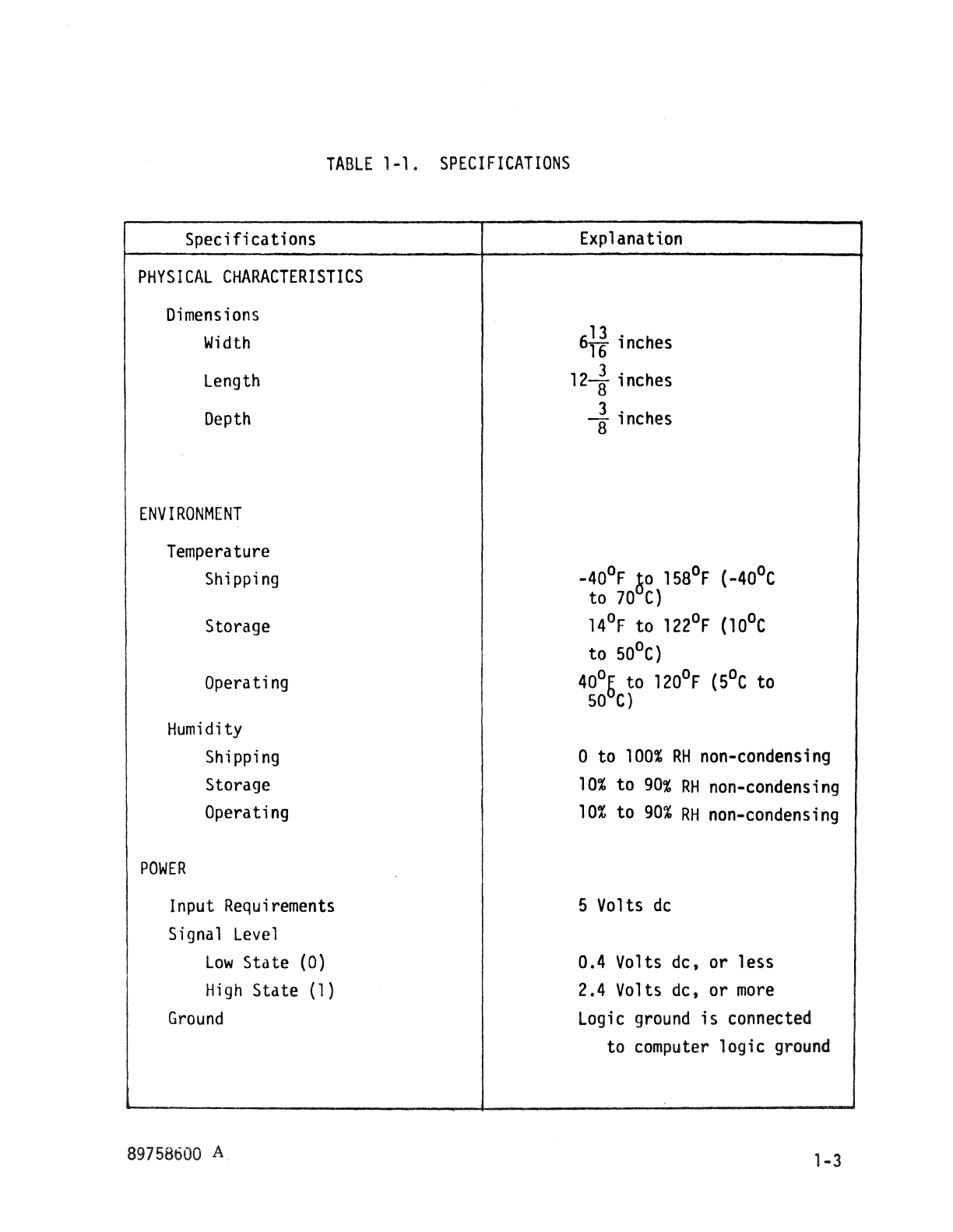
TABLE
1-1.
SPECIFICATIONS
Specifications Explanation
PHYSICAL
CHARACTERISTICS
Dimensions
Width
length
Depth
ENVIRONMENT
Temperature
Shipping
Storage
Operating
Humidity
Shipping
Storage
Operating
POWER
Input
Requirements
Signal level
Low
State (0)
High
State
(l)
Ground
89758600 A
6
13.
h
16 lnc es
12
~
inches
~
inches
-40°F
~o
158°F
(-400e
to
70
C)
14°F
to
122°F
(lOoe
to
50
0e)
40
0b to
120°F
(Soe
to
50
e)
o to
100%
RH
non-condensing
10%
to
90%
RH
non-condensing
10%
to
90%
RH
non-condensing
5 Volts
dc
0.4 Volts dc, or less
2.4 Volts dc, or
more
Logic
ground
is
connected
to
computer
logic
ground
1-3

OPERATION
AND
PROGRAMMING
89758600
IA,
SECTION
2
OPERATION
AND
PROGRAMMING
Programming
of the
AT310-A
TTL
A/Q-DSA
Bus
Expander
is
not
required. Refer to the
1784
Computer
Reference
Manual
or to
the
AB107/AB1OB
Computer
Customer
Engineering
Manual
and
the
reference or customer engineering
manuals
of
the controllers
to
be
used
with the system,for
programming.
Refer to Section 3 for
installation,
checkout
and
operation
of the
bus
expander.
2-1

,(
\
(
"
\
(
INSTALLATION
Unpacking
SECTION
3
INSTALLATION
AND
CHECKOUT
1. Carefully
remove
wrapping
from
the
AT310-A
TTL
A/Q-DSA
Bus
Expander
PWA's.
Check
for physical
damage
to
each
and
record
damage
on
the packing
list.
Cneck
that
part.
numbers
agree with
packing
list.
2.
Remove
wrapping
from
cable
and
check
for physical
damage.
Record
damage
on
packing
list.
Check
that
part
number
agrees with
packing
list.
Physical Limitations
Care
must
be
taken to prevent
damage
to the
bus
expander
PWA's.
They
must
not
be
f1exed
t bent or
dropped.
Power
Requirements
The
bus
expanders require
+5
vdc
derived
from
the
power
supply of the
AB107/AB108.
Cabling
and
Connectors
An
external interconnecting
flat-cable
is
available for
use
between
the
controller
and
the distribution unit.
The
cable part
number
is
89821800.
It
is
approximately four
feet
long.
89758600
A
3-1
Where
two
sets
of
expander
PWA's
are required,
two
sets of
flat
cables
must
be
installed.
Cooling
Requirements
The
expander
PWA's
are cooled
by
the forced
air
system
of the enclosure.
No
further cooling
is
required. Refer to the
computer
customer
engineering
manual
(89633300)
for further information concerning cooling
capabilities
of
the
computer
and
expansion enclosure.
Environmental
Considerations
The
environmental considerations necessary for operation (or storage) of the
controller cards are
listed
in Table 1-1.
Preparation
and
Installation
To
install
the
TTL
bus
expanders
perform
the following
with
the
computer
power
switched "off":
1.
Remove
the air-flow blocks
from
lower
slide
of card
slots
to
be
used
in
both
the
main
and
remote
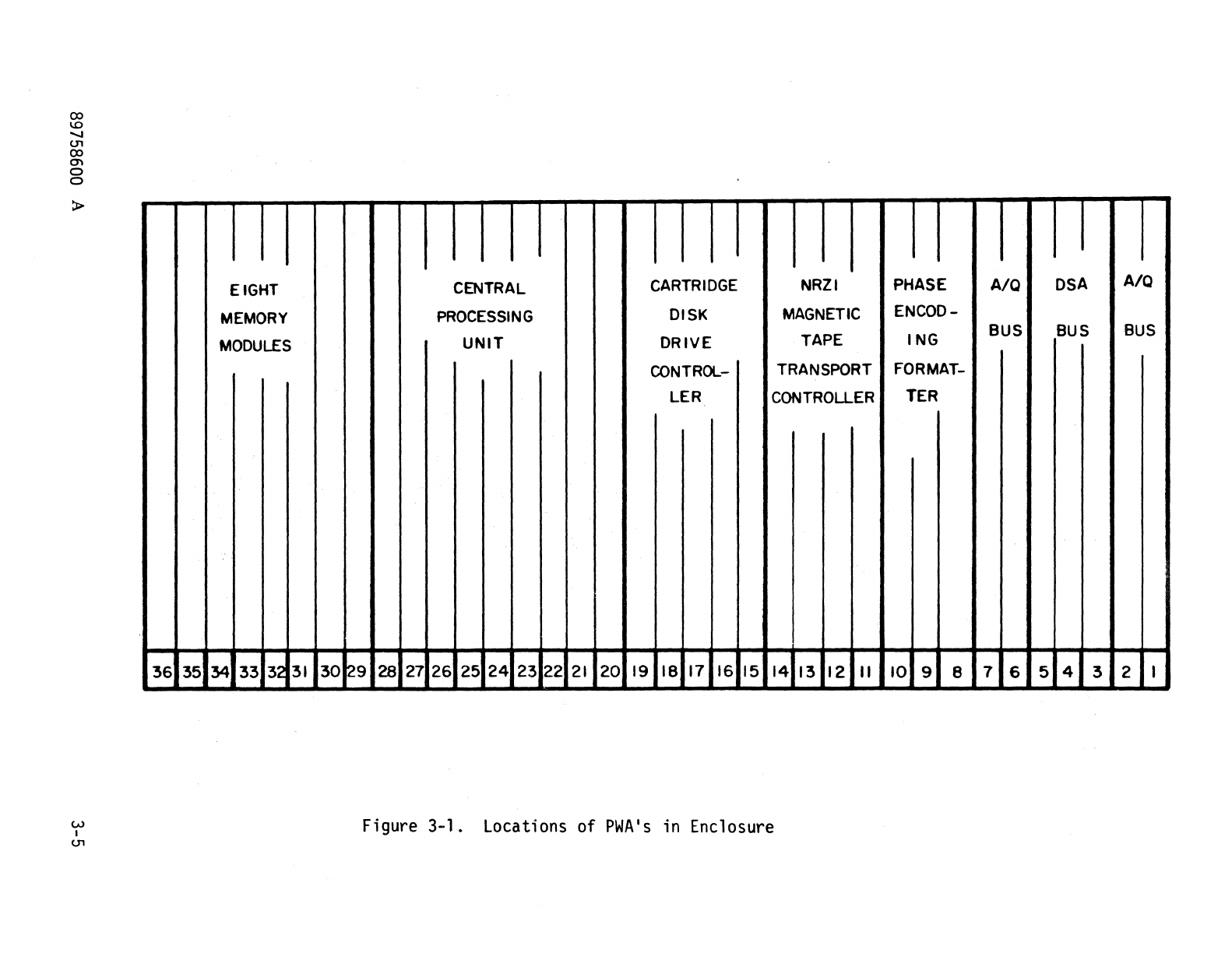
enclosures. Refer to Figure
3-1
for selection of
the location for
PW
board.
2.
Inspect both enclosures, card
slots,
PW
board
slides
and
connector pins,
for physical
damage.
3.
Place the internal
select
jumpers
in
the positions
on
each
PWA's
as
descrjbed
below
and
shown
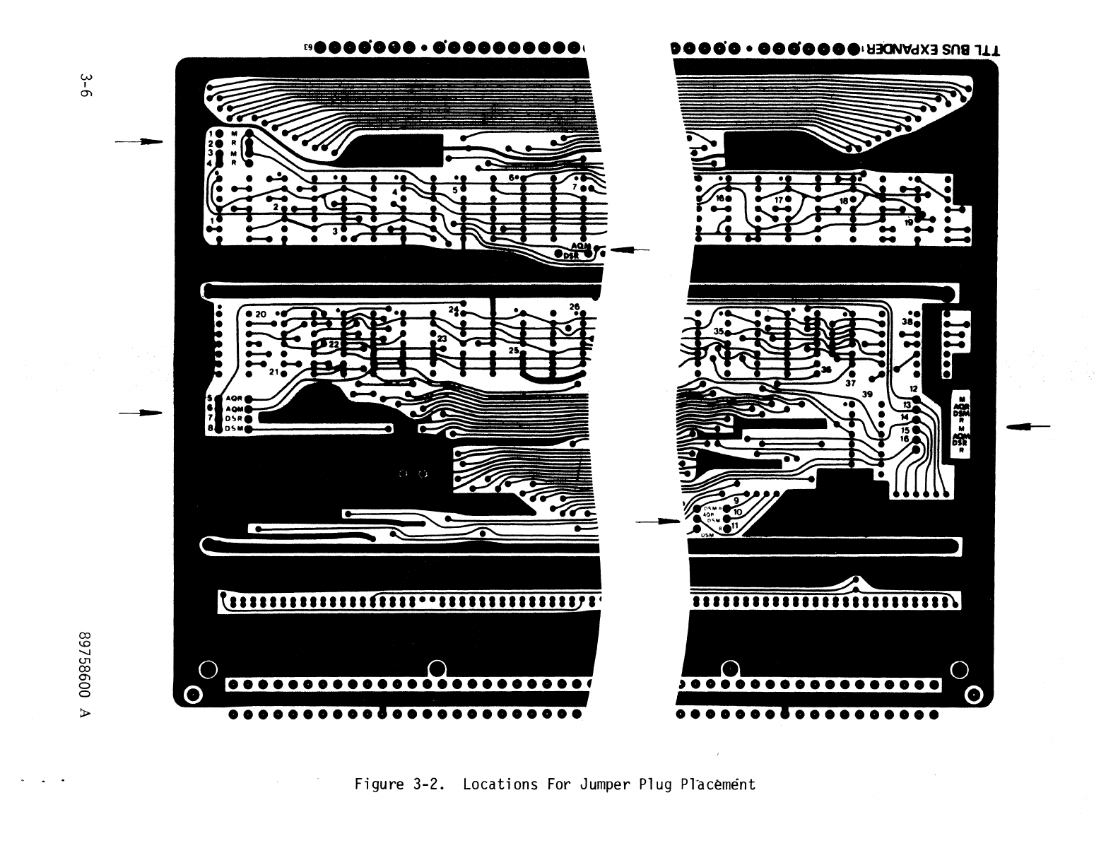
in Figure 3-2:
3-2
89758600
A
For
A/Q
expansion:
/,.-/
..
-
..
-.-::-:-::=::::.-".~
On
the
main
enclosure
PWA
(89821600
O(89876~.9J/
1)
At
Ul, place
jumper
plugs
at
1
and
at~both
marked
M)
2)
Below
U6-U7
(~rked
AQ~),
place
jumper
plug.
3)
Below
U20,
place
jumper
plug
at
6
(marked
AQM).
4)
At
U40,
place
jumper
plugs
at
12,
15
and
16
(marked
M,
M
and
AQM
res pecti
ve
ly) .
On
the
remote
enclosure
PWA
(89759200
or
~~.QJ
1)
At
Ul,place
jumper
plugs
at
2
and
at
4
(marked
R).
2)
Below
U6-U7
(marked
AQM-DSR)
place
jumper
plug.
3)
Below
U20,
place
jumper
plug
at
5
(marked
AQR).
4)
Below
U34-U35,
place
jumper
plug
at
9
(marked
R),
at
10
(marked
AQR)
and
at
11
(marked
R).
5)
At
U40,
place
jumper
plugs
at
13,
14
and
17
(marked
AQR,
Rand R respectively).
For
DSA
expansion:
On
the
remote
enclosure
PWA
(89759200
or
89880700)
1)
At
Ul,
place
jumper
plugs
at
2
and
at
4 (both
marked
R).
2)
Below
U6-U7
(marked
DSR-AQM),
place
jumper
plug.
3)
Below
U20,
place
jumper
plug
at
7
(marked
DSR).
4)
Below
U34-U35,
place
jumper
plug
at
9
(marked
R)
and
11
(marked
R).
5)
At
U40,
place
jumper
plugs
at
16,
14
and
17
(marked
R,
DSR
and
R respectively).
On
the
main
enclosure
PWA
(89821600
or
89876000)
1)
At
Ul, place
jumper
plugs
at
1
and
at
3 (both
marked
M).
2)
Below
U20.
place
jumper
plug
at
8
(marked
DSM).
3)
Below
U34-U35,
place
jumper
plug
at
9, 10
and
11
(marked
DSM).
4)
At
U40,
place
jumper
plugs
at
12,
13
and
15
(marked
M,
DSM
and
M,
respectively).
89758600
A
3-3
CAUTION
Do
not
install
cables or expanders
PWA's
in
computer
enclosure or
expansion enclosure with
power
on.
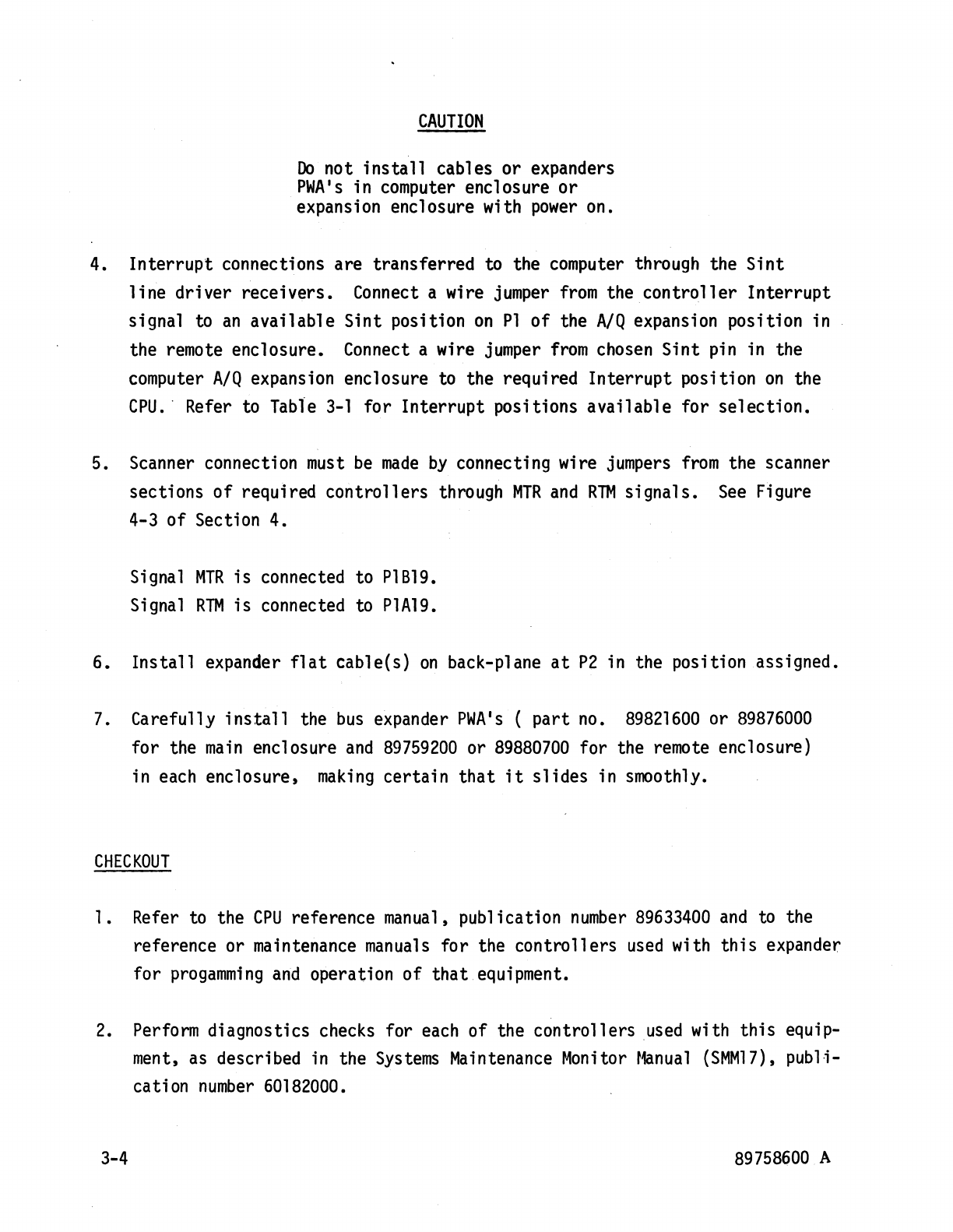
4. Interrupt connections are transferred to the
computer
through the Sint
line
driver receivers.
Connect
a wire
jumper
from
the
controller
Interrupt
signal
to
an
available Sint position
on
Pl
of the
A/Q
expansion position in
the
remote
enclosure.
Connect
a wire
jumper
from
chosen
Sint
pin
in
the
computer
A/Q
expansion enclosure to the required Interrupt position
on
the
CPU.·
Refer
to
Table
3-1
for Interrupt positions available for selection.
5. Scanner connection
must
be
made
by
connecting wire
jumpers
from
the scanner
sections
of
required controllers through
MTR
and
RTM
signals.
See
Figure
4-3 of Section 4.
Signal
MTR
is
connected to
P1B19.
Signal
RTM
is
connected to
P1A19.
6.
Install
expander
flat
cable(s)
on
back-plane
at
P2
in the position assigned.
7.
Carefully
install
the
bus
expander
PWA's
( part
no.
89821600
or
89876000
for the
main
enclosure
and
89759200
or
89880700
for the
remote
enclosure)
in
each
enclosure,
making
certain
that
it
slides in smoothly.
CHECKOUT
1. Refer
to
the
CPU
reference
manual,
publication
number
89633400
and
to
the
reference or maintenance
manuals
for the controllers
used
with
this
expander
for
progamming
and
operation of that equipment.
2.
Perform
diagnostics
checks
for
each
of the controllers used with this equip-
ment,
as
described
in
the
Systems
Maintenance
Moni
tor
r1anua1
(SMMl7),
publi-
cation
number
60182000.
3-4
89758600
A
ex>
1.0
......
U'l
ex>
0'1
o
o
>
W
I
U'l
36
35
EIGHT
MEMORY
MODULES
34
33
32
31
30
CENTRAL CARTRIDGE NRZI
PROCESSING
DISK
MAGNETIC
UNIT
DRIVE
TAPE
CONTROL- TRANSPORT
LER
CONTROLLER
29
28
27
26 25
24
23 22
21
20
19
18
17 16 15
14 13
12
"
Figure 3-1. Locations of
PWA's
in
Enclosure
PHASE
A/Q
DSA
A/Q
ENCOD-
ING
BUS
BUS
BUS
FOR MAT-
TER
10
9 8 7 6 5 4 3 2 I
W
I
O"l
co
~
'-I
Ul
co
O"l
o
o
>-
£s
••••••••••••••••••
'
•••••
•
•••••••
1
~3CJNvdX3
sna
1ll
........-
Figure 3-2. Locations
For
Jumper
Plug
Plac~ment
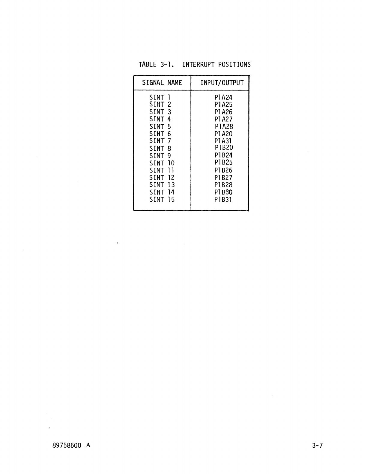
TABLE
3-1.
INTERRUPT
POSITIONS
SIGNAL
NAME
INPUT/OUTPUT
SINT
1
P1A24
snn 2
P1A25
SINT
3
P1A26
SINT
4
P1A27
SINT
5
P1A28
SINT
6
P1A20
SINT7
P1
A31
SINT
8
P1B20
SINT
9
P1B24
SINT
10
P1B25
SINT
11
P1B26
sun
12
P1B27
SINT
13
P1B28
SINT
14
P1830
SINT
15
P1831
89758600
A
3-7

SECTION
4
THEORY
OF
OPERATION
INTRODUCTION
This section presents general
and
detailed functional descriptions
of
the
equipment, using aids
such
as
overall
and
detailed block diagrams.
Descriptions are
keyed
to the detailed logic
diagrams
in the
diagram
section (Section
5)
and
afford"a basis in understanding the detailed
description
of
the specific
circuit
in
that
section.
89758600
A
NOTE
It
is
assumed
that
the reader
is
familiar with
Control
Data
equipment
and
with
the
programming
characteristics
of the
Computer
as described
in the
1784
Computer
System
Reference
Manual,
Publication
Number
89633400.
4-1
GENERAL
The
AT3l0-A
TTL
A/Q-DSA
Bus
Expander
i~
comprized of
two
standard
50-PAK
PWA'3
and
a single interconnecting
flat
cable.
Both
PWA's
use
the
sampe
type of
board, but
have
different
components.
The
main
PWA
is
installed
in the
AB107/AB108
enclosure with
its
jumper
plugs placed as described in Section 3, while the
remote
PWA
(with
jumper
plugs
set)
is
placed in
either
the
BT148-A
expansion
enclosure or another suitable enclosure.
The
function of
each
expander
is
set
by
placing
or
omitting
jumper
plugs
from
the positions
shown
in Figure 3-2.
Access
in
and
out
of
the enclosures
is
made
by
leading the
flat
cable
through the
slots
in the case
on
the backside of the enclosures.
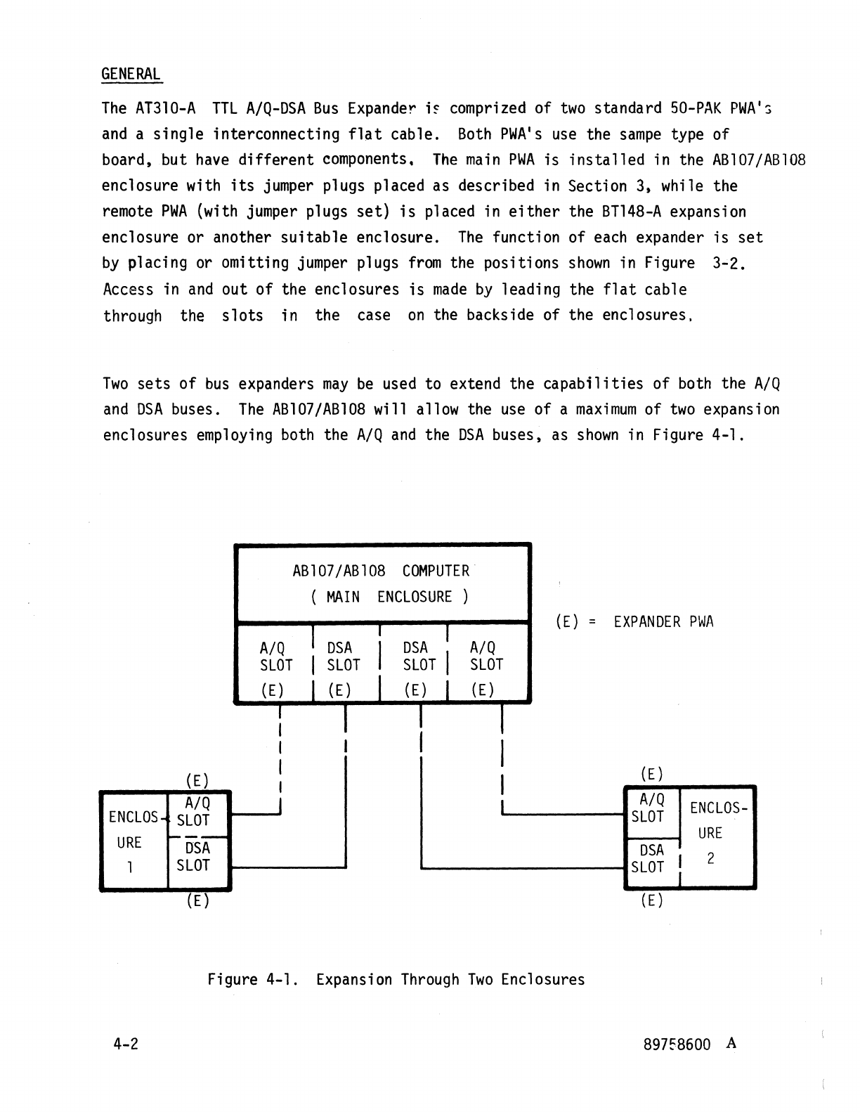
Two
sets
of
bus
expanders
may
be
used
to extend the
capabilities
of
both
the
A/Q
and
DSA
buses.
The
AB107/AB108
will allow the
use
of a
maximum
of
two
expansion
enclosures
employing
both
the
A/Q
and
the
DSA
buses,
as
shown
in Figure 4-1.
ENCLOS
URE
1
4-2
(E)
A/Q
SLOT
---
DSA
SLOT
(E)
A/Q
SLOT
(E)
I
I
J
AB107/AB108
COMPUTER
(MAIN
ENCLOSURE)
(E)
=
EXPANDER
PWA
I
(E)
I
A/Q
ENCLOS-
SLOT
URE
DSA
I 2
SLOT
J
(E)
Figure 4-1.
Expansion
Through
Two
Enclosures
897f8600
A
CIRCUIT
TYPES
The
circuits
used
in the
TTL
expanders are
bi-directional.
Signals
may
enter
from
PI
and
exit
at
P2
or enter
P2
and
leave
at
Pl.
Four
types of
line
driver
circuits
are used.
Type
1
utilizes
a
146S
inverter in series with a
204
inverting
AND
gate. This
circuit
is
symetrical.
Line
driver
Type
2 uses
an
inverter
(146S)
and
an
inverting
AND
gate
(204)
in the
circuit
from
PI
to
P2,
while the signal
flow
from
P2
to
PI
passes through
an
inverting Schmitt Trigger (167), shaping the
signal
first
and
then through
an
inverting
AND
gate.
Type
3
uses
only inverting
AND
gates
(204
1s) in
each
of the signal paths
and
both paths are symetrical.
Type
4
uses
a
NAND
Buffer with the inputs to
each
AND
gate section paralleled in
the
circuit
from
PI
to
P2,
and
an
inverting
AND
gate
(204)
in the
P2
to
PI
circuit.
These
circuits
are
shown
in Figure 4-2.
89758600
A 4-3
vee
270
Mounted
only
on
PWA
in
remote
enclosure
'vee
270
-
-
Mounted
only
on
PWA
in
remote
enclosure
4-4
Control Signal
Bus
to
Li
ne
__
---1
1465
~--I-----I
a
20~~
XXX
XXX
~--~
vee
330
.....
-_.----(
P2
a
----...&..11..204
I
~--~~146S~~
XXX
XXX
1--
__
Control Signal
Line
to
Bus
LINE
DRIVER
-
TYPE
1
Control Signal
Bus
to
Line
a
1
204~~-----
_-
.......
1465
I-l---
.....
--I
XXX
XXX
a
---~1-204
SCHMITT
1-------1
TRI
GGER
11----
1 7
xxx~--
Control Signal
Line
to
Bus
LINE
DRIVER
-
TYPE
2
Figure 4-2.
Line
Driver Circuit
Types
560
VCC
330
89758600
A.
Mounted
only in
PWA
in remote enclosure
vee
Mounted
only
on
PWA
in remote enclosure
Control
Si
gnal
Line to
Bus
LINE
DRIVER
-
TYPE
3
Control Signal
Bus
to
Line
8
204
XXX
8
XXX
JE
Control Signal
Line to
Bus
LINE
DRIVER
-
TYPE
4
vee
330
560
-
Figure 4-2. Line Driver Circuit
Types
(continued)
P2
89758600
A.
4-5
4-6
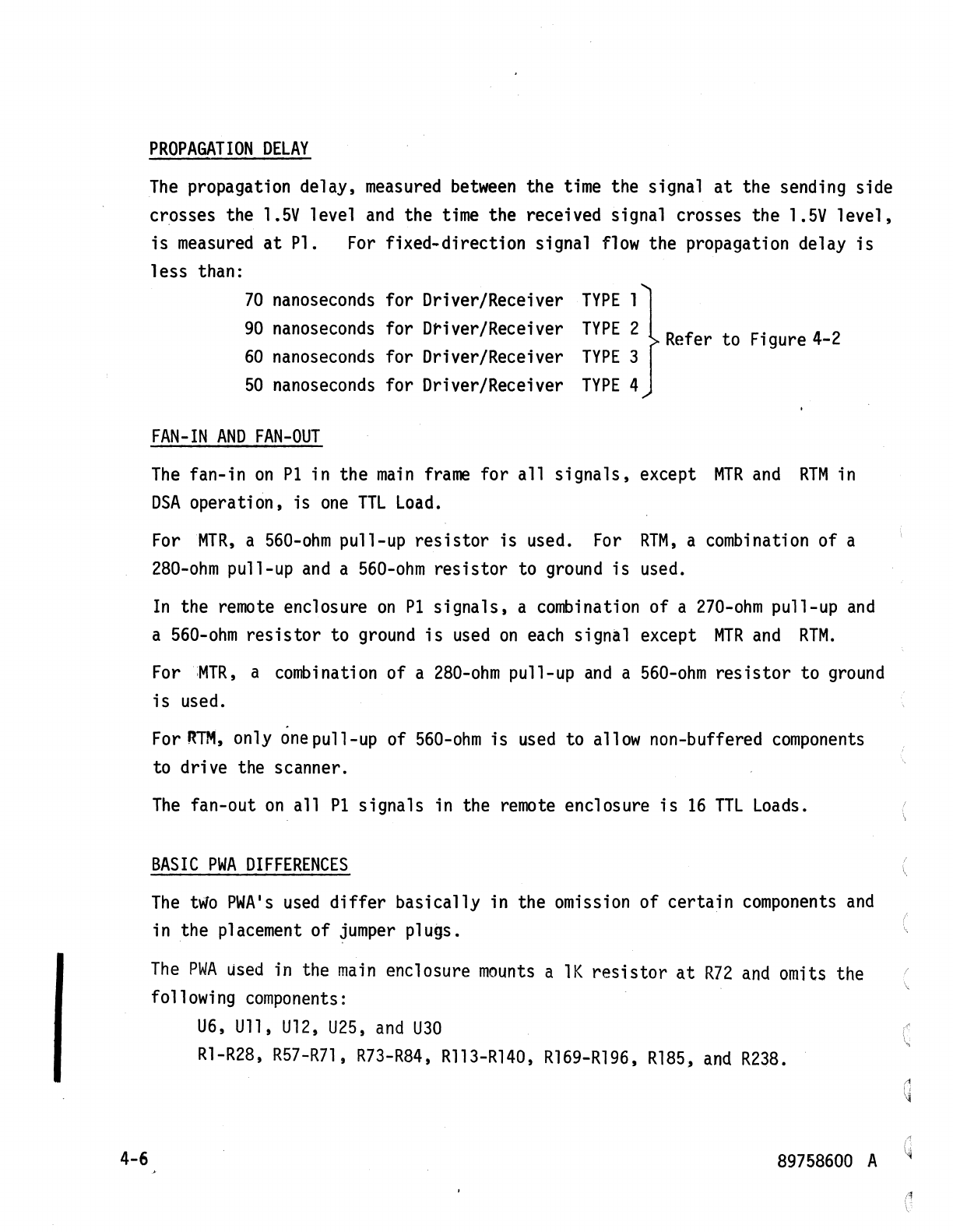
PROPAGATION
DELAY
The
propagation delay,
measured
between
the time the signal
at
the sending side
crosses the
1.5V
level
and
the time the received signal crosses the
1.5V
level,
is
measured
at
Pl.
For
fixed-direction signal flow the propagation delay
is
less
than:
70
nanoseconds
for
Driver/Receiver
TYPE
1
90
nanoseconds for Driver/Receiver
TYPE
2 Refer to
Fi
gure 4-2
60
nanoseconds
for
Driver/Receiver
TYPE
3
50
nanoseconds
for
Driver/Receiver
TYPE
4
FAN-IN
AND
FAN-OUT
The
fan-in
on
PI
in the
main
frame
for
all
signals,
except
MTR
and
RTM
in
DSA
operation,
is
one
TTL
Load.
ForMTR, a
560-ohm
pull-up
resistor
is
used.
For
RTM,
a combination of a
280-ohm
pull-up
and
a
560-ohm
resistor
to
ground
is
used.
In
the remote enclosure
on
PI
signals,
a combination
of
a
270-ohm
pull-up
and
a
560-ohm
resistor
to ground
is
used
on
each
signal except
MTR
and
RTM.
For
,MTR,
a combination of a
280-ohm
pull-up
and
a
560-ohm
resistor
to
ground
is
used.
For
RTM,
only
one
pull-up of
560-ohm
is
used
to allow non-buffered
components
to drive the scanner.
The
fan-out
on
all
PI
signals in the
remote
enclosure
is
16
TTL
Loads.
BASIC
PWA
DIFFERENCES
The
two
PWA's
used
differ
basically
in the omission of
certain
components
and
in the placement
of
jumper
plugs.
The
PWA
used
in the
main
enclosure
mounts
a
lK
resistor
at
R72
and
omits the
following
components:
U6,
Ull,
U12,
U25,
and
U30
Rl-R28,
R57-R7l,
R73-R84,
Rl13-R140,
R169-R196,
R185,
and
R238.
89758600
A
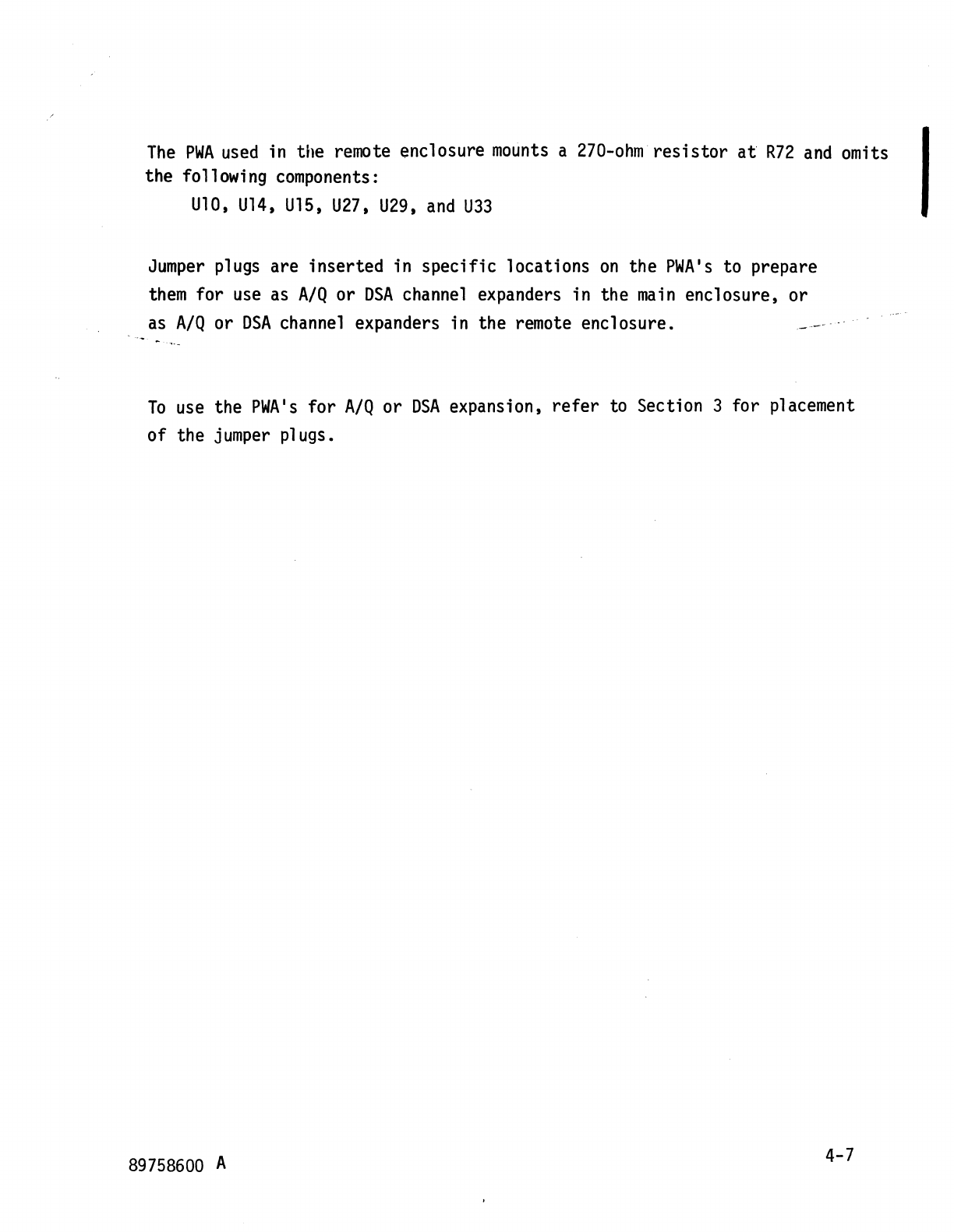
The
PWA
used
in the
remote
enclosure
mounts
a
270-ohm
resistor
at
R72
and
omits
the following
components:
U10, U14, U15, U27, U29,
and
U33
Jumper
plugs
are inserted in specific locations
on
the
PWA's
to prepare
them
for
use
as
A/Q
or
DSA
channel
expanders in the
main
enclosure, or
as
A/Q
or
DSA
channel
expanders in the
remote
enclosure.
To
use
the
PWA's
for
A/Q
or
DSA
expansion,
refer
to Section 3 for placement
of the
jumper
plugs.
89758600
A 4-7
I
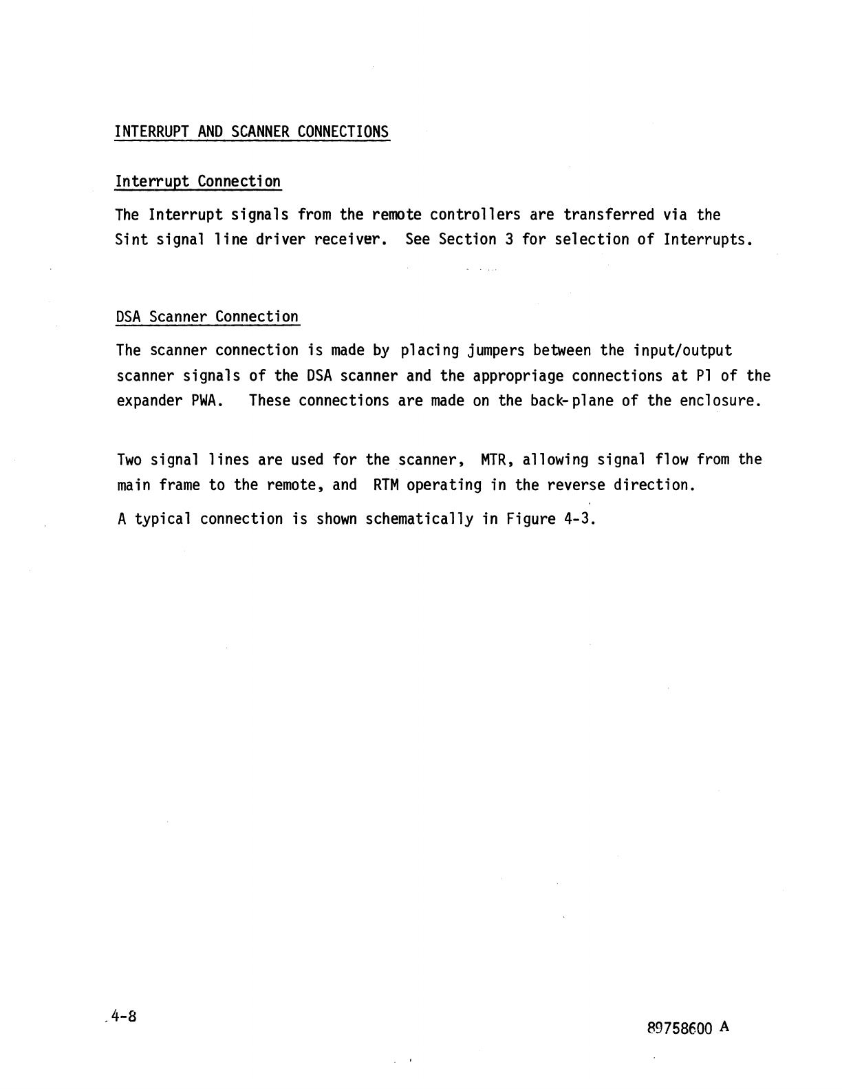
INTERRUPT
AND
SCANNER
CONNECTIONS
Interrupt Connection
The
Interrupt signals
from
the
remote
controllers are transferred via the
Sint signal
line
driver receiver.
See
Section 3 for selection of Interrupts.
DSA
Scanner Connection
The
scanner connection is
made
by
placing
jumpers
between
the input/output
scanner signals of the
DSA
scanner
and
the appropriage connections
at
Pl
of the
expander
PWA.
These
connections are
made
on
the back-plane of the enclosure.
Two
signal lines are
used
for the scanner,
MTR,
allowing signal
flow
from
the
main
frame
to the remote,
and
RTM
operating in the reverse direction.
A typical connection
is
shown
schematically in Figure 4-3.
89758600
A
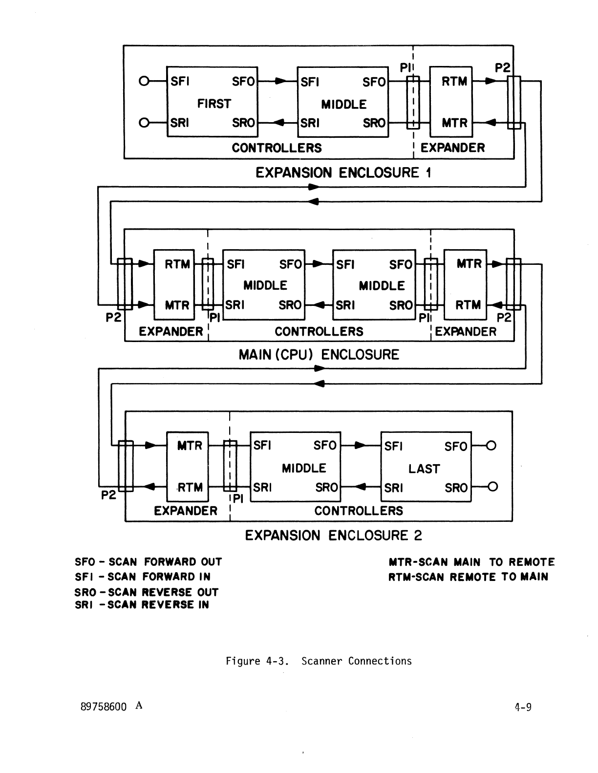
I
I
PII
P2
0-
SFI
SFO
..
SFI
SFO
r+
RTM
..
~
--
I
FIRST
MIDDLE I
I
0-
SRI
SRO
-
SRI
SRO
MTR
-
I"
--
CONTROLLERS :
EXPANDER
EXPANSION
ENCLOSURE
1
..
-
-
-
I :
I I
-
RTM
rL
SFI
SFO
-
SFI
SFO
r+
MTR
..
-I -I -
I I
I
MIDDLE
MIDDLE I
..
I
..
I
..
P2-
MTR
Tpi
SRI
SRO
SRI
SRO
":t-
RTM
-
~I-
PII
P2
EXPANDER:
CONTROLLERS
: EXA\NDER
MAIN
(CPU)
ENCLOSURE
..
-
-
I
I
1"'1-
..
MTR
r+
SFI
SFO
..
SFI
SFO
--{)
-I -
I
MIDDLE
LAST
I
-
,RTM
I
SRI
SRO
-
SRI
SRO
--0
P2
--
!PI
-
EXPANDER
:
CONTROLLERS
SFO
-
SCAN
FORWARD
OUT
SFI -
SCAN
FORWARD
IN
SRO
-SCAN
REVERSE
OUT
SRI
-SCAN
REVERSE
IN
89758600 A
EXPANSION
ENCLOSURE
2
MTR-SCAN MAIN
TO
REMOTE
RTM-SCAN REMOTE TO MAIN
Figure 4-3. Scanner Connections
4-9
SIGNAL
ROUTING
The
direction of signal
flow
of
all
signals except data lines
is
determined
by
jumper
plugs
set
on
the
expander
PWA's
according to
PWA
use
(A/Q
main,
A/Q
remote,
DSA
main,
DSA
remote).
The
data signal
flow
direction
is
determined
by
the combination of the
jumper
plug
settings
and
the
state
of
the
Read
signal for
A/Q
expansion, or the Write
Enable
for
DSA
expansion.
Refer to Section 3
and
Figure 3-1 for location of the positions for the
jumper
plugs.
The
following
lists
provide the signal data
flow
direction:
A/Q
expansion
Data
lines:
Normally
flowing
from
main
enclosure to
remote
enclosure.
When
the
Read
signal
is
present the direction
is
reversed.
Signals
from
main
enclosure to
remote
enclosure:
Address
lines,
Timing
Pulse,
Me,
W=O
Reaa,
Write,
Program
Protect
Signals
from
remote
enclosure to
main
enclosure:
Sint
lines,
Char
Input, Reject,
Reply
DSA
expansion
Data
lines:
Write
Enable
active
from
remote
enclosure to
main
enclosure
Write
Enable
not active
from
main
enclosure to
remote
enclosure
Signals
from
main
enclosure to
remote
enclosure:
Protect Fault, Autoload,
MC,
Resume,
Par
Error,
Par
Bit,
Protect Bit,
65K
Memory,
SMTR.
Signals
from
remote
enclosure to
main
enclosure:
4-10
MemorY.Address
lines,
Request,
~P-rl~·0-r-'i7ty-,
Protect,
Write
Enable,
SRTM.
89758600
A
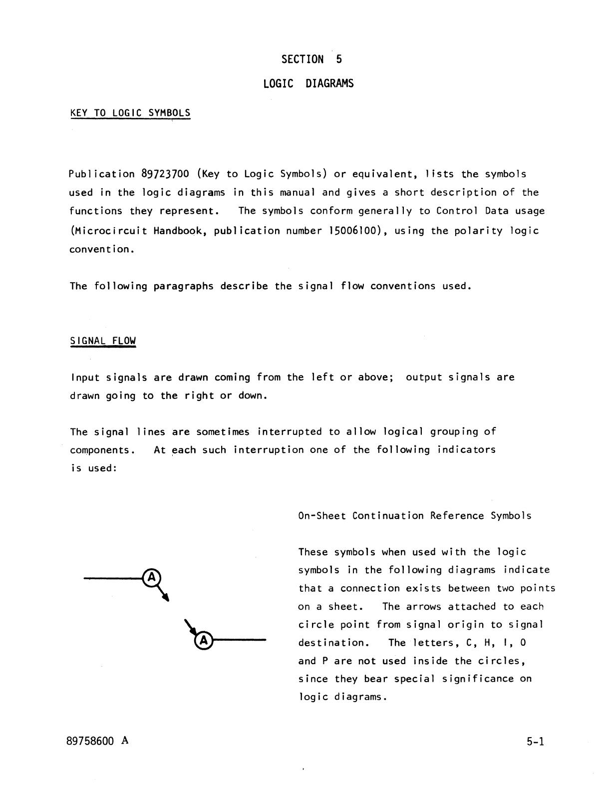
KEY
TO
LOGIC
SYMBOLS
(
SECTION
5
LOGIC
DIAGRAMS
Publication
89723700
(Key
to
Logic Symbols)
or
equivalent,
lists
the
symbols
used in
the
logic
diagrams in
this
manual and
gives
a
short
description
of
the
functions
they
represent.
The
symbols conform
generally
to
Control
Data usage
(Microcircuit
HandboQk,
publication
number 15006100),
using
the
polarity
logic
convention.
The
following
paragraphs
describe
the
signal
flow
conventions
used.
SIGNAL
FLOW
Input
signals
are
drawn coming from
the
left
or
above;
output
signals
are
drawn going
to
the
right
or
down.
The
signal
lines
are
sometimes
interrupted
to
allow
logical
grouping
of
components.
is
used:
89758600 A
At
~ach
such
interruption
one
of
the
following
indicators
On-Sheet
Continuation
Reference
Symbols
These symbols
when
used
with
the
logic
symbols in
the
following
diagrams
indicate
that
a
connection
exists
between
two
points
on a
sheet.
The
arrows
attached
to
each
circle
point
from
signal
origin
to
signal
des
tina
t
ion.
The
letters,
C,
H,
I,
0
and P
are
not
used
inside
the
circles,
since
they
bear
special
significance
on
logic
diagrams.
5-1
(ON
SHEET
2)
---@3.6
2.3
0--
(ON
SHEET
6)
OR
5-2
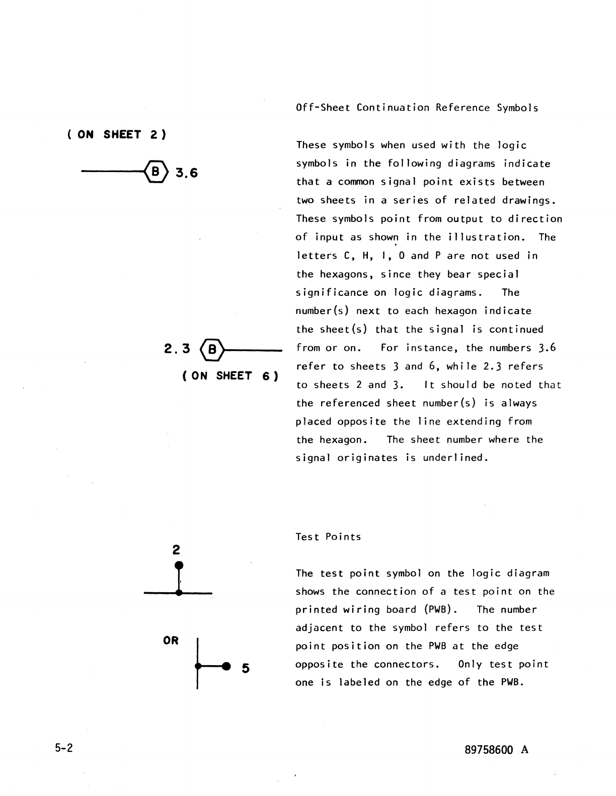
Off-Sheet
Continuation
Reference
Symbols
These symbols
when
used
with
the
logic
symbols in
the
following
diagrams
indicate
that
a
common
signal
point
exists
between
two
sheets
in
a
series
of
related
drawings.
These symbols
point
from
output
to
direction
of
input
as
show~
in
the
illustration.
The
letters
C,
H,
I,
0 and P
are
not
used in
the
hexagons,
since
they
bear
special
significance
on
logic
diagrams.
The
number(s)
next
to
each hexagon
indicate
the
sheet(s)
that
the
signal
is
continued
from
or
on.
For
instance,
the
numbers 3.6
refer
to
sheets
3 and
6,
while
2.3
refers
to
sheets
2 and 3.
It
should
be
noted
that
the
referenced
sheet
number(s)
is
always
placed
opposite
the
line
extending
from
the
hexagon.
The
sheet
number where
the
signal
originates
is
underlined.
Test
Points
The
test
point
symbol on
the
logic
diagram
shows
the
connection
of
a
test
point
on
the
printed
wiring
board
(PWB).
The
number
adjacent
to
the
symbol
refers
to
the
test
point
position
on
the
PWB
at
the
edge
opposite
the
connectors.
Only
test
point
one
is
labeled
on
the
edge
of
the
PWB.
89758600.A
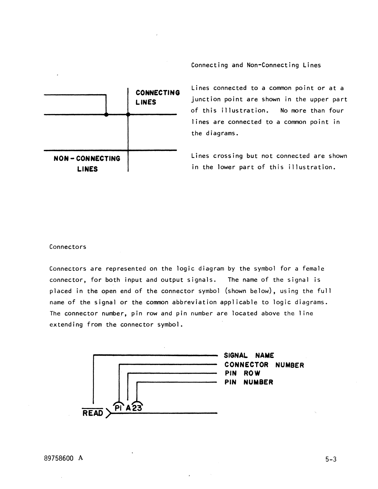
NON -CONNECTING
LINES
Connectors
CONNECTING
LINES
Connecting and Non-Connecting Lines
Lines
connected
to
a
common
point
or
at
a
junction
point
are
shown
in
the
upper
part
of
this
illustration.
No
more
than
four
lines
are
connected
to
a
common
point
in
the
diagrams.
Lines
crossing
but
not
connected
are
shown
in
the
lower
part
of
this
illustration.
Connectors
are
represented
on
the
logic
diagram
by
the
symbol
for
a female
connector,
for
both
input
and
output
signals.
The
name
of
the
signal
is
placed
in
the
open end
of
the
connector
symbol (shown
below),
using
the
full
name
of
the
signal
or
the
common
abbreviation
appl
icable
to
logic
diagrams.
The
connector
number,
pin
row
and
pin
number
are
located
above
the
1 ine
extending
from
the
connector
symbol.
READ
>>-P_I_!_~_:------
89758600 A
SIGNAL
NAME
CONNECTOR NUMBER
PIN ROW
PIN NUMBER
5-3
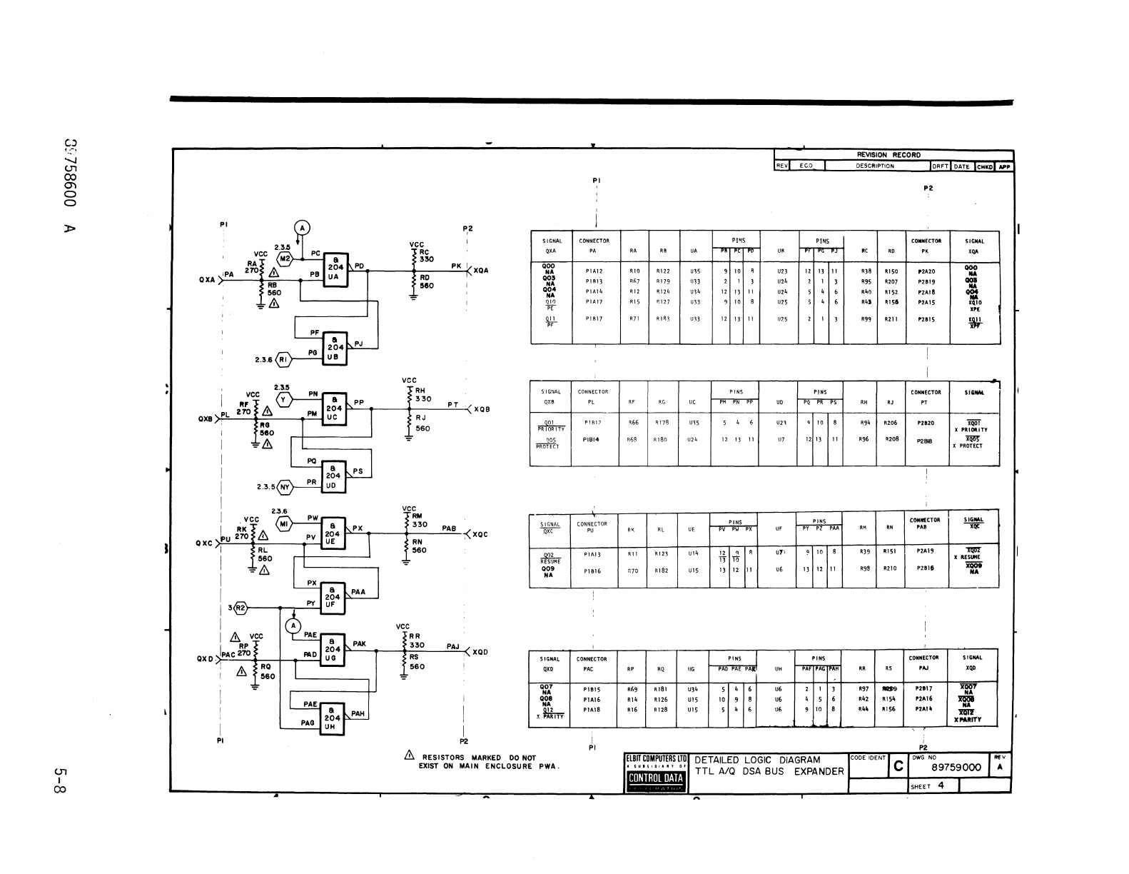
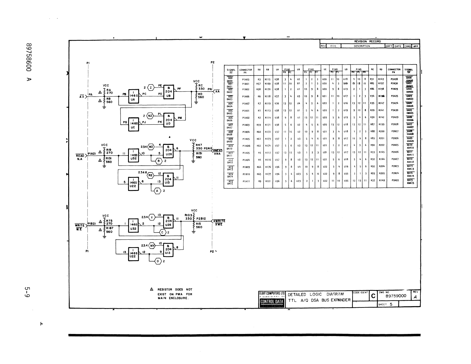
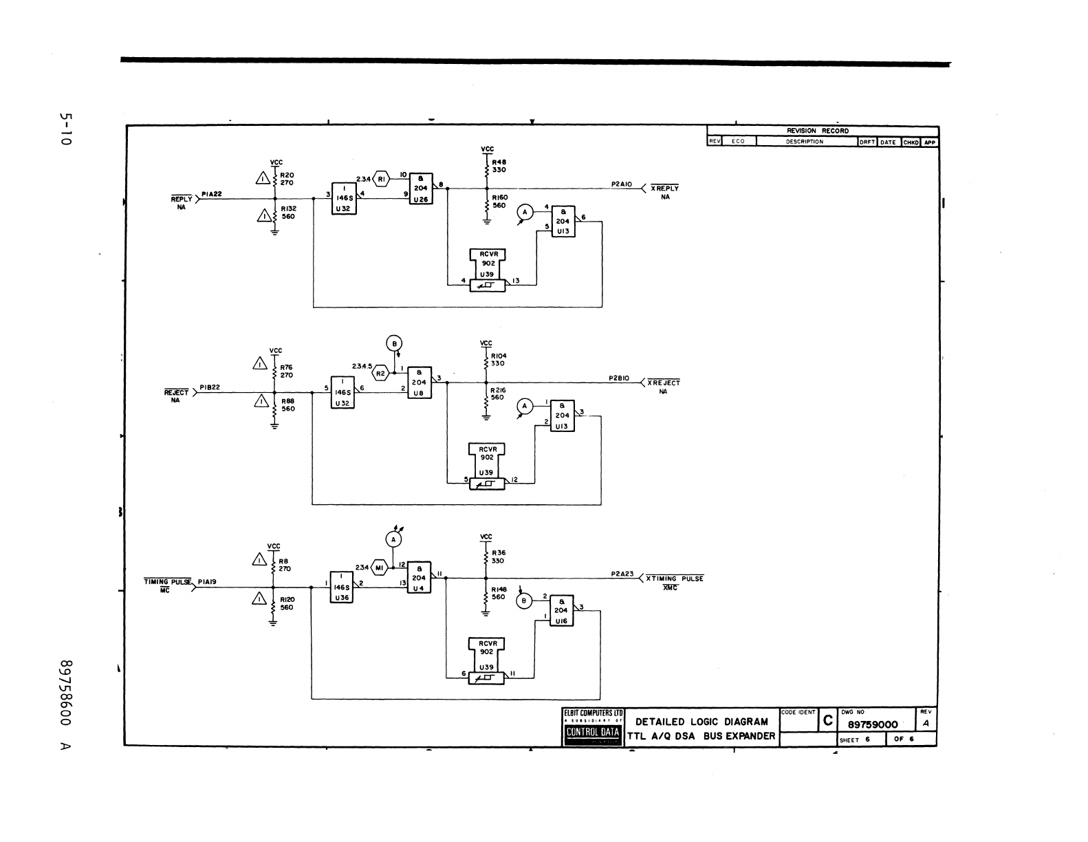
LOGIC
DIAGRAM
89759000
Each
circuit
of the
AT3l0-A
TTL
A/Q-DSA
Bus
Expander
is
bi-directional.
The
flat
cable
is
connected
from
P2
of
one
enclosure to
P2
of the other.
The
presence or lack
of
jumper
plugs determine the direction
and
conditions of
signal flow.
As
stated
in Sections 3
and
4, during
use
in the
main
enclosure
PWA
89821600
will
have
all
jumper
plugs
marked
M
installed.
PWA
89759200,
mounted
in
the
remote
expansion enclosure will
have
all
jumper
plugs
marked
R
set.
When
the
PWA
in the
main
enclosure
is
used
for
A/Q
expansion,
all
jumper
plugs
marked
AQM
will
be
set
and
the
PWA
in the
remote
enclosure will
have
all
AQR
jumper
plugs
set.
For
DSA
operation the
main
enclosure
PWA
will
have
the
DSM
jumper
plugs
set
and
that
installed
in the
remote
enclosure will
have
the
DSR
jumpers
set.
The
jumper
plugs are
used
to
either
enable or
inhibit
the inverting
AND
gates
in one-half of
circuitry
or the
other,
causing the signal flow to occur
from
Pl
to
P2,
or
from
P2
to Pl.
The
gate(s)
shown
in the logic diagrams, herein,
in the upper
part
of
each
circuit
allows the signals to flow
from
Pl
to
P2,
when
enabled.
At
this
time the
AND
gate(s)
shown
in the lower
part
of
each
circuit
will
be
inhibite~.
For
signal
flow
from
P2
to Pl, the
lower
half of
each
circuit
is
enabled
and
the upper
half
inhibited. Control of
all
but the
data
circuitry,
inhibiting or enabling
one
half
or the
other,
is
accomplished
through the
jumper
plugs
set
at
U40.
Flow
of data in
either
direction
is
controlled
by
the
READ/WRITE
circuitry
(sheet 5
and
sheet 2,
lower
half)
The
circuitry
used
herein
is
of the four types described previously in Section 4.
89758600
A 5-4
00
u:.
-....J
U1
00
0'\
0
0
» I jlFF-SHEE1'I
REFERENCE
LETTERS
-RI
R2
MI
M2
Y
NY
Z
NZ
A
8
C
0
I
.
I
,\
U1
I
U1
SHEET
L'CATIONS
2 " 4 5 6
0-1
...
C-4
C-4
0-3
0-1'"
8-4
8-4
8-4
c-;!
0-1.
0-4
8-4
8-3
C-19
8-4
0-4
C-4
C-I",
0-4
C-4
...!.:!.
C-I.
C-4
8-4
10-4
A-I.
0-4
A-I",
C-4
B-2
8-"'"
8-2
C
-3.
8-2
B-391
B-2
10-3
...
P2A"
I
+5V)
J I IVCC
..
C9
C2
..
C8
~
~;:F
'T'
68
NF
GND}
P2A_29___
.
aND)
PI8U
8HD)
P2A05
8HD)
P2821
i
i
~
10
0
0
..
..
CD
I:
NGITES'
1 SHEET REVISION STATUS
laoToJjj6111:1~;;41
.
REVISION
RECORD
DESCRIPTION
IDAFT
r"TE
IClOCDI
...
REDRAWN
TO
CDC
STD
I,,"
1"-""
1_1)1;
\rI~'
..
R
72
IN
MAIN
PWA
ADDED
1m
[rJ
I
ilCKI047
ftA~'
D TOTAILE ftl
SH>,
".~,1\I
..
,II.Iw..L
AAAAAA
IIIIIH5NY.HIDSHS"
1M
2 :
IN
'.ADDED
TO
Itl
AND
II
IN
I
ADDED
TO
NY
:~~'.
~i~~:,~
U:'~:;J:~'
1t10_.
R211,
PZI07
IMS
"-4
INPUT
NY
ADDEO
AT
UIS-IO
OUTPUT
0
ADDED
AT
U22-12
f04lCK
1072
:::~~:
:'E:::'~
'OR
RE'iO!
[<ToKIO.'
TO
FIT "SSY.
THREE
SEPARATE
CIRCUITS
ot4
NEW
SH6
REPLACE
I I
1A
I
GENERAL
CIRCUIT
AND
TABLE
ON
l.
J'.".
/J
~'rxEL~~~\RIGHT(CONYERSK'IN......
_ q
...
ISHEET
LOCATIONS
FOR
RI,R2.MI
~N.!._U~~.~TED
IN
SHI TABLE,
_
ERRORS
CORRECTED
NO
lOGIC
CHANGES.
[)£TAILS
IN
[CO
,,~I~\'iG1iA
I
I.
SIGNAL
REFERENCES
IN TABLES
AND
qlNNECTORS:
z'
0,
NA
INDICATES
NIl
SIGNAL TRANSMITTED,
UPPER
SIGNAL NAMES IN TA8LES
AND
liN
CIINNECTORS
REFER
TI!
A/Q
SIGNALS
WHEN
PWA
IS
USED
TG
EXPAND
A/Q
L'WER
SIGNAL
NAMES
IN.
TABLES AND
liN
CGNNECTGRS
REFER
U DSA SIGNALS WHEN
PWA
IS
USED
Til
EXPAND OSlo,
NGIT
MGUNTED
IN
REM!IlTE
PWA,
UIO, UI4,
U15,
U27,U29,U33
NIIT
MII)UNTED
IN
MAIN
PWA,
us,
un,
U12, U25,
U30
4,
...
DENOTES
SIGNAL
ORIGIN
5,
ALL
RESISTORS
ARE
Y4
WATT,
5%
------
i
r--
DETAILED
LOGIC
UNLESS
OTI£RWlSt
SPECIFEO
DIMENSION
ARE
IN
INCHES
..
~
TOLERANCES TTL
A/Q
DSA
UI
3 PLACE 2
PLACE
ANGLES
DIAGRAM
BUS
!I~I!
~~~~~R,S
I!i
I FIRST
USED
J TITLE
.111111;11111/;11
AT
310 - A
0
I-
EXPANDER
..
~
• ± ±
0
CD
Q 00
NOT
SCALE
DRAWING
DWN
CD
~
MATERIAL
CHKO
' , r
DDE
ID~T
I c I
DRAW~G
NO
..
u
CD
i5
NIA
~GR
' .
...
".'
89759000
Q MFG
FINISH
>-
NIA
APPR
1
lSH[[T
<t
SCALE
I'
co
1.0
"'-J
(,)'1
co
en
o
o
:t>
(,)'1
I
en
PI
I
006
) PIAIS
_.-
{
'I
REQUEST I '
---2!.L)
PIBIS
AUTOLn
A I
VCC
.&
R72
~
RTM
I
~
I
I
I
I
I
I
I
o~lR:37
VCC
r
-::I
[560-
~
RI7
l.o
7
r---l
560
LD~~
I~0t.~~
J
12
LOCATED
BfLOW
U34-
35 RI29
560
L-,
vce
&.
d¥i
)PIBI9
LOCATED
BELOW
U34-3S
I
I
PI
NOTES
&
R23B
560
r::-'
,----,
I
C..ESM,j
560
~~R73
_ RIBS
vec
-
560
&,
R72
ON
MAIN
PWA
IS IK
R72
ON
REMOTE
PWA
IS
270
&.
RESISTORS
ARE
NOT
MOUNTED.
a
r
R41
330
RI53
560
P2AI71
XQ06
XREQUEST
VCC
&.
XQI3
I"
XAUTOLAO
I
L-l
I
rr
-II
1"'&'''"
p.P~·--j-<11
°AQM I
RI57
I
,
D~
-.J
560
BELOW
1)6-
U7 I
r-J
I
XQI4
XRTM
£1
a
5
xxx
~
6 , - - - {
P2BII
UI4 <
RI3
560
XQI5
XMTR
I
P2
&~
JUMPER
PLUG
M~ST
NOT
BE
IN
DURING
AQR
-
DSM
OPERATION
IN
CIRCUIT
ON
PWA
FOR
MAIN
ENCLOSURE
5
vec
®
,-_
_
fR22S
RI
5.4.6
,---,
I
560
::::®
oM
0 I RI
12
VCC
I
R22'l
I ® 3.4.5.6
,---,
I
560
®
M a R2
15
I
/"
I
~~I
:dMI
(17)
I
R22/
CC
,---,
560
I ®
R
<>--
M
3.4.5
VCC
14
LOCATED
BELOW
U20
vec
DETAILED
LOGIC
DIAGRAM
TTL
A/Q
DSA BUS
EXPANDER
3.4.5
ex>
\D
-....J
(J'1
ex>
0'\
0
0
»
(J'1
I
-....J
?
PI
I
I
iiiffiii
PI824
AD1
XA
XC
I
I
I
~
I
vee
I
RN
I 2t1,!1,6lR2
XD
)PAB
270
~
W
,.
I
.&.
~
XF f'AY
.&.
PI
Re
33D
PH
I
XA
RD
560
RL
330
PAA ,
XC
RM
5&0
vec
RY
IY~~,
\
330
PAJ .
(iii
RZ
560
RU
330
PBF
RV
560
I
P2
XF
5IG~I,~,L
XA
pROt.
pRtJi£ti
AOOB
~
ADOO
SIGi!,l,L
xc
1::;0
PRnT!:CT
mmT
AD03
!mlTrr
ADO'
SI!IT1T
AOO6
mTOl
AD12
mmlb
ADI.
I
STN'rn8
NA
SIGr~L
'0
lIIO"1IIPUT"
NA
=
A005
=
A007
=
AD11
lmI11!7
AD15
=
ADl3
SIGNAL
XF
mmr
AD02
=
ADO'
mn'I!2"
~AD10
~
RESISTOR
DOES
NOT
EXIST
ON
PWA
FOR
MAIN
ENCLOSURE.
PI
I
CONtlECTOR
RA
RB
UA
PA
PIAl3
R21
RI33
U31
Plff.23
R77
R189
U31
C01i;:ECTOR
RJ
RK
UE
PT
P1A2Q
RIB
Rl30
U33
P1E26
RaD
R192
U31
P1B27
RBI
R193
U3D
P1B30
'83
R19S
ua
ftAll
R25
R137
U20
i'lA30
R27
R139
~30
P1B20
.7'
RIS6
UJ4
CONNECTOR
RN
RP
UG
PAB
PlaD7
'63
R175
U16
P1BZS
R82
R194
U11
PIB31
R84
R196
UI1
P1A26
R24
R136
U12
PlA31
R2B
R14D
UI1
PIAIB
R26
mB
U11
CONNECTOR
.w
RX
UN
PAY
P1B25
'7'
RI91
U12
P1A24
R22
RI34
U12
P1A25
R23
R135
U12
~2
PHI)
U,
pm
RC RD
COr!NECTOR
S
IG~!Al
I
PE
I'C
PO
PE
PF
PG
PH
XA
,
10
a
ua
4 5 6 R4'
R161
P2AO'
p~.:al
12
13
11
U2B
4 5 6
R10S
R277
P2B~6
I
PHIS
UF
PINS
RL
RM
cormECTOR
SI~.G,L
PU PV
PH
PX
py
PZ
PAA
5 4 6
U25
121311
R46
R158
PlA13
11M)
1PIIII'Im"
2 1 3
U27
,
10
a
Rloa
R220
P2BOS
~1
121311
U29
12
13
11
R109
RZ21
P2B04
XSIHT04
mIT
2 1 3 U2' 2 1 3
R111
R223
P2B02
,=6
,
10
a
U29
9
10
B .53 '165
P1905
XSINT12
ml!Il[
XSINT14
5 4 6 U2' 5 4 6 .55
R167
P1B02
DIm
IG
e
U:::6
2 1 3
RI02
R214
P2B13
'SIMTOB
NA
PINS
UH
'IN<
'Q
RR
CONNECTOR
SIGNAL
PAC
PAD
PAE
PAF
PAG
PA"
PAJ
iID
10
, a
U4
1 2 3
R91
R203
P2B2Z
XCHAR
INPUT
NA
12 13
11
Ul0
131211
Rno
R222
PlB03
XSINT13
xmJ5"
1 2 3
UID
2 1 3
R112 R223
P2BOI
XSINT15
DNl7
12 13
11
ua
131211
.52
R164
P2A06
XSINT03
DD1T
5 4 6 Ul0 5 4 6 .56
R168
P2AOl
XSINT07
DIlTS"
,
10
8
UlO
,
10
8
R;'
"166
P2A04
XSINT05
AD13
,
'TN<
UP
PI"
RY
.Z
CONNECTOR
SIGNAL
PAZ
PDA
PBB
PBe
PBD
PBE
PBF
lF
5 • 6
U27
2 1 3 RI07
R219
R2B08
XSINno
mr
,
10
a
U27
5 • 6
.50
R162
P2A08
XSINTOI
mIIJ
1 2 3
U27
121311
'51
R163
P2An7
XSINT02
= -

CJ
,:..-,
"-J
<.n
co
0)
o
o
»
<.n
I
CO
PI
,.
, P,2
SIGNAL
QXA
PK ! XQA
000
.A
RO
003
580
.A
00'
.,
QIO
K
QII
"
-
vee
2.3.5
RH
S I
GrlAL
~f
330
PL
270
PT
QXB
XQS
RJ
560
QXB
~
PR
IORITY
0.05
P'R'O'fITr
vee
RM
330
PAB
~
XQC
2.3.6
I
I .
VCC
I
RK
SIGNAL
---qxc-
p'
n , +
RN
'
560
oxc >PU 270 -
i
hio
I
r"
I!:..J
~
RESUME
00'
I
I
I
I
I &
vcc
I
RP
OXD.~C270
,
&lROII,n-1
I
PI
.A
L---
V!RR
~
::0
PAJ
.(
XQO
SIGNAL
560
QXO
007
.A
008
.A
9.!..1..-
x
PAR
tTY
P2
& RESISTORS
MARKED
00
NOT
EXIST
ON
MAIN ENCLOSURE
PWA.
I
I
PI
CONNECTOR
PA
RA
P1A12
RIO
P1RI3
,"
P1A14
'"
PIA
17
Rl5
PIB17
Pll
CONNECTOR
Pl
PF
P1Bl?
%6
PIBI4
R68
CONNECTOR
PU
"
PIAl3
Rli
P!
816
[;70
~--~
,
CONNECTOR
PAC
P1B15
PIA)6
PIAIB
I
PI
RP
'69
".
,,'
"
UA
RI22
u15
R179
UB
R124
u14
P,12l
u33
RIA3
U33
PO
UC
1<1713
U15
R 180 u14
-
RL
UE
R123
u"
RI82
UI5
RQ
'"
RIBI
UJ4
RI26
UI5
R12B
UI5
P2
Pt~IS
PINS
ClHtNECTOR
SiGNAL
"'
""
"
RD
PK
XI,,,
9
10
, " IJ
II
'"
R150
P2AZO
QQO
U2j IIA
2 I J u24 , I J
'95
R207
P2B19 -
IIA
12
13
II
u24 5
~
,
,"
R152
P2AI8
~
9
10
8
U25
5
~
, R4I
R156
P2AIS "QIO
...
i
12 13
II
U?5 , I J
'"
R211
P2BIS
Wr'-
PINS
PINS
CONNECTOR
SI;NM,
PM
PH
PP
UO
PQ
PR
PS
RH
RJ
PT
5
~
,
un
,
10
8
,,~
R206 P28Z0
XQot
K PRIOftITY
12
Il
II
"7
12 13
II
,,.
R208
P2B1B
~
x
PROTECT
--
-~------
-I
PIHS PINS
CONNECTOR
SIGML
PV
PW
PX
UF
py
PZ
PAA
RH
RN
PAS
XliC
"I
'
II'
u7
II
8
'39
Rl51 P2Al9
'!1IU2'
OTD
X
RESuttE
13 12
11
u6
13 12
11
R38 R210
P2Bl6
iQOi
N'
_
'--'-~L-
~-
-----
PINS PINS
CONNECTOR
SIGNAL
PAD
AE
PAl(
UH
PAF
PA
IPAH
RR
RS
PAJ
'QD
5
~
6
u6
2 I J '97
--
PUll
-
.,
10
9 8
u6
• 5 6
,"
R15~
P2,t,,16
lla
NO
5 4 ,
u,
9 10 8
."
RIS6 PZAlit 11M
XPAIUrr
~------.i.....-"""--_
-
Of v
A

00
\D
-...J
<..TI
00
0'1
o
o
»
<..TI
I
\D
..
PI
I
I
I
- I
PA
AXr
I
I
I
I
vee
I vee
READ>
PIA21
III.J
~!i'o
I
N.A '
>R131
III.
>580
vee
I
III.
R75
WRITE
PIB21
270
ii:T I
III.
:~~
PI
P2
I
I
vee I
Re
I
I)."
.
~
330
PN
(Xl:
,
RD
560
I
vee
R47
I
330
P2AI2
RI51
~XNA
5110
vee
RI03I
I
~..
330
P2B12 (liWIIITl
, RI5 I
ifWl
560
III.
RESISTOR
DOES
NOT
EXIST
ON
PWA
FOR
MAIN ENCLOSURE.
I
I
P2 '
SIGNAL
AX
Aoo
DADO
A1!r
DAD
I
AlIr
DAOl
;mr
DA03
ToO
DA04
A05
DAD5
"Ali6
DA06
-w
DAD7
"liD!"
DA08
....
DAD9
-;:ro
0.10
A1T"
DAII
Air
DAll
om
Ai1i
DA14
Al5
DAI5
CONNECTOR
PA
PIA03
PI801
P1802
P1A06
PlA07
PIAOI
PIA02
PIB03
P1804
P1805
P1806
PIAOS
PIA04
PIB09
PIB10
PIAII
RAIRBluA
R31
RII5I
U38
R57
R169
UlS
R58
RllO
U38
R6
I
Rile
I
U37
R7
I RII9 I
U36
RIIRI13IU]8
RZ
IR114
I Ule
R59
I
Rill
I
U38
R6D
I
Rl72
J U37
R61
I
RI73
I
U37
R62
I
R174
I
U37
R5
fRIl71
U37
R4
IR1I61
U37
...f.!.IlL
PBl'E
31
4
Il
10
13112
13112
,18
11110
516
13112
, I 8
U.
U2
UI
UI
U3
U4
UI
ul
U2
U2
U3
U3
U3
U,
PINS I
uc
PO
lPf""
U20
U2.
10
I 9 18 I
U20
10
I , I 8 I
U2I
61U22
" I 6 I
U20
13
112
III
I
U20
61u20
10
I 9 I 8 I
UZI
61u21
13112111
IU21
2 I 3 I
U4!1
13
112
111
I
U21
PINS I
ua
II
110
IUi8
4 3
UtI
9 8
UI,
11
110
IUl7
2 I
u16
UI9
5 1 6 1 ui9
131121uI8
4 I
U18
9 I B I
U17
UI7
13
112
I
u1]
5 I 6 1
U18
R64
I
RI76
1
U36
I , 1 8 1
U4
1
10
1
,I
8 1
U22
I 3 I 4 1
ul6
R65
1
RI77
1
U36
1 3 1 , 1
U23
1 5 1 4 1 6 I
U22
1
,I
8 I
U35
PINS
I
RC
I
RD
m:-
'liD
18
1'3
1 IR143
I~
12
II
11.85
11.197
11.86
Rlg8
'13
1'3'
I.",.
13112111
1'35
IRI'1
9 110 I 8 I
R29
111.1"'1
5 I
..
I 6
111.30
111.142
13112111
111.87
111.199
11.88
I
11.200
\0
I 9 I 8 I
R8g
I
11.201
5 I 6 I
R90
I
RZ02
13112111111.33
111.1115
..
I 6 I
11.32
I
11.\.4,.
51 6 I
11.92
I
11.20,,"
] I
R9}
I
11.205
Kg
I
11.121
I
U36
61
u23
U22
I
II
110
I
U35
I
12
J
13
J
11
I
11.37
J
Rllt'
DETAILED
LOGIC DIAt:;R,\M
CONNECTOIt
P.
P2A28
P2130
P1l29
PZAl5
P2A2"
P2A)O
P2A2,
P2828
P2827
P2I26
P2825
P2AZ6
P2Al7
PlBZ]
P2B2'"
PZAZZ
SIGNAL
lA
1Aiiii
..
.-L
....
.....
-mJ"
....
,
"1lIIIO
.-
xm-
....
5
---
xDA06
"iA07
x""'7
"Dlir
ic
....
"iA09
XDA.,
"iAlii"
loAlO
-mr
_II
-mr
....
"
mr
llOAI)
1m"""
XDA'"
mr
IMIS
TTL
A/Q
DSA
BUS
EXPANDER
I
I-I
--,
_n__
I'"
\n
I
a
00
\.D
-....J
\n
00
'"
a
a
»
R~LY.
> PIA2Z
Rf.jffi
NA
TIMING
PU
lie
PIB22
PIAI9
vee
~TR20
270
&~~:
vee
&
R76
270
& R88
560
vee
&TR8
270
& RI20
560
vee
.,-
vee
R48
330
RI60
~
RI04
330
R21S
'60
vee
R36
330
RI48
560
13
~
XiiEP'Lv
---------
NA
P2BI0
P2A23
XREJECT
NA
XTIMING
PULSE
~
DETAILED
LOGIC
DIAGRAM I I - I
""'v""""
,~
A/Q
DSA
BUS
EXPANDER
I
SCOPE
SECTION
6
MAINTENANCE
This section supplies references
and
procedures for the maintenance of the
equipnent
listed
in Section 1 of
this
manual.
TOOLS
AND
SPECIAL
EQUIPMENT
The
following
is
a
list
of maintenance tools required for
this
equipment:
Pllrt r Part Description Quantity
Number
8968B700
Board
Extender 1
U96J0300
UOllrd
Extractor 1
O~cilloscope
1
Digital
Voltn~ter
1
PUBLICATIONS
The
publications
listed
below
are applicable to maintenance of
this
equipment.
Publication
PUb.
No.
I
1784
Computer
Reference
Manual
89633400
AU107/AU10B
Computer
Custaner Engineering
Manual
89633400
liDO Callputer
System
Codes
Manual
60163S00
System
~1aintendnce
Monitor
(SMMl7)
601U2000
MAINTENANCE
Preventive maintenance of a
PW
assembly
is
not required. After
it
is
deter-
mined
that
a
PW
assembly has
failed,
the
PWA
should
be
replaced
by
an
ident-
ical.
trouble-free
PWA.
For
replacement
of
a
PW
assembly,
refer
to
Section 3
of
this
manual. After replacement, a diagnostic
check
should
be
performed as
des cri
bed
in
SMM17.
89758600
A
CAUTION
Do
not
remove
or replace
PWA's
or cables with system
power
ON.
6-1


SECTION
7
MAINTENANCE
AIDS
(Not
Required)

SECTION
8
PARTS
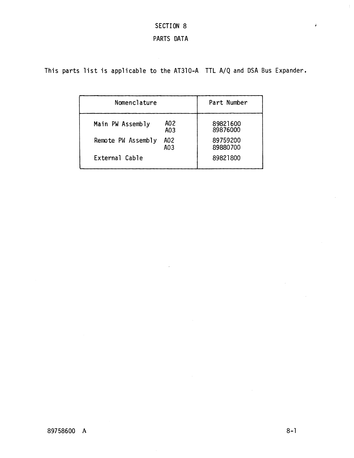
DATA
This parts
list
is
applicable to the
AT310-A
TTL
A/Q
and
DSA
Bus
Expander.
Nomenclature
Part
Number
Main
PW
Assembly
A02
89821600
A03
89876000
Remote
PW
Assembly
A02
89759200
A03
89880700
External
Cable
89821800
89758600
A
8-1


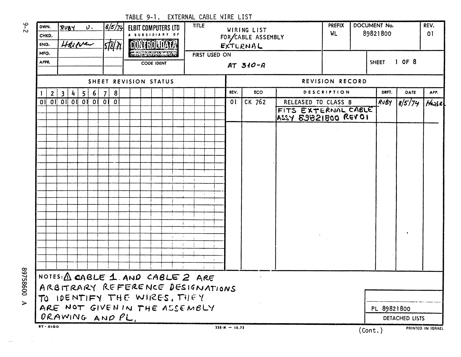
SECTION
9
WIRE
LIST
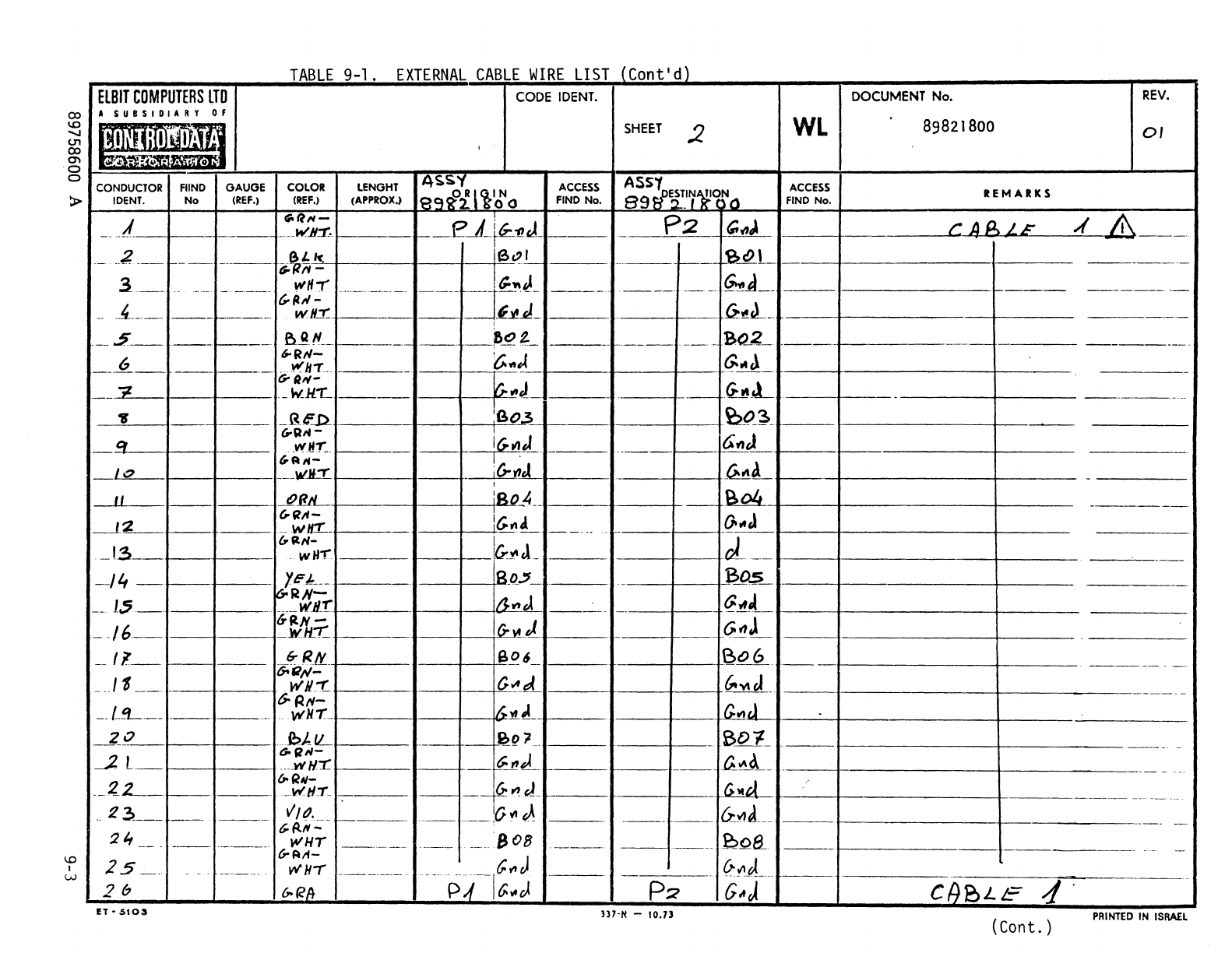
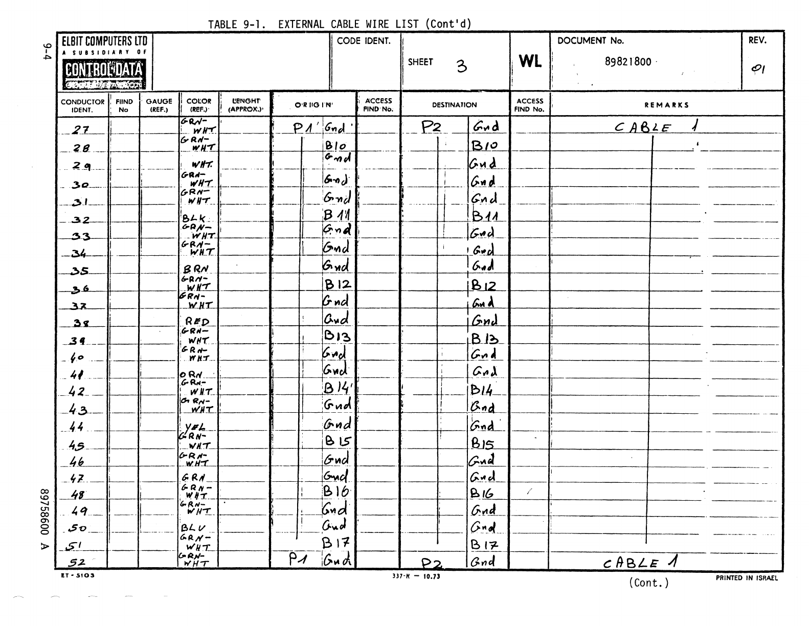
The
wire
list
included in this section
is
applicable to the
AT3l0-A
TTL
A/Q
and
DSA
Bus
Expander.
Wire
size, color, origin, destination
and
name
of signal
normally
found
on
that
wire
are included in the
table.
A
pin
list
for
each
of the
PWB's
is
also included
in
this section.
89758600
A 9-1
~
I
N
00
~
.......
c.n
00
0'1
o
o
>
I
TABLE
9-1.
EXTERNAL
CABLE
WIRE
LIST
OWN. 1?!l6j
U.
S/5"/l!!
HBIT
COMPUTERS
LTD
TITLE
PREFIX
DOCUMENT
No.
REV.
--
WI
RI
NG
LI
ST
CHKD. A
SUBSIDIARY
OF
FO~CABLE
ASSEMBLY
WL
89821800
01
ENG.
J..I.tA(~
f/ifJi
OOHIJ;
Ukl~f.6!
E)(Tt:~NA
L
MFG.
~~~~~~
FIRST
USED
ON
APPR.
CODE
IDENT
AT
3.fO-R
SHEET
t
OF
8
SHEET
REVISION
STATUS
REVISION
RECORD
1 2 3 4 5 6 7 8 I
REV.
ECO
DESCRIPTION
DRFT.
DATE
APP.
01 01 01
01
01
0 0 0
01
CK
762
RELEASED
TO
CLASS
B
f~1J8y
8/si7lf
fktU.·
FITS
E~"E:RN#\L
CASL!i;:
-
ASS.
'I
8..ge21
gao
REt
0 ,
I !
I
_.
-
1--
I
I
.-
I I
! I i i i
i I ! I
! -
,
! ,
i I ! :
i , !
'--J-
! : , ! . ,
. ,
: I i !
, .
, i
I i ! i
I
I I I I
I I I
I I I I I ! ! I I -
-.
NOTES:&,
(lAB.Lt:
~.
AND
CABLEi"' 2
ARI:
A
~
B
IT
r<.A
t<.
'(
rtr:·FE:~rE
Nc.t:"
DES.
J
GNAT"
ONS
To
'0
E
Nil
1='1
rEi
E W J
.~EAS
, 141 F
'{
----------
AR.E
NO,-
G,Vf;
tJ
,
"J
TH
€
A~.~E
MeL'!
PL
89821800
OR-AWING-
ANO
I'L,
DETACHED
LISTS
I!T'/SlOO
33S-N -
10.73
(Cant. ) PRINTED
IN
ISRAEL
00
1.0
......
U'I
00
Ol
a
a
>
1.0
I
W
InUI-a...
~-I.
LI\II-I"'"&...
"',"U",'-L..
n.a.n,,-
... .1....."
\,IVI.""
\001
HBIT
COMPUTERS
LTD
CODE
IDENT
•
•
SUBSIDf.Rl
Of
..
SHEET
2
WL
1
I
CONDUCTOR
FUND
GAUGE COLOR lENGHT
4SS_X
ACCESS
ASS't
ACCESS
IDENT.
No
(REF.)
(REF.)
(APPROX.)
leq~:l'
i't
0
FIND
No.
89
iff;l~17'fP9~
~
FIND
No.
_
...
tl
~fll'l
I--_e~_.~~~t..t
P.2
~~
..
.
_-
._.
__
WJJ~ .
._
...
2
__
f---
-----
--tL
k. ie", -
..
_--1-------
~c!)t_
fi.
IY-
----1~~
.3.
__
.
-------
III"'"
-.-
..
-~.-----.-.
----
...
----.-----
~.d
__
._--
_.
-~--.-
6-~"';'
~~rl_.
f----.
wH:r
I
.
__
.2._
f-----.
&JUL .
1--._--
60t
B<L2_
.--
f---,
-,-
...
--
------
-.---
..
-_
..
-
--~-
6-RN-
{;YI,.(
~
..
J_
--.-
....
~h7_.
-
-.
f.i-(M-
};"J
-;z
._k(}l"L
----
. -.
._--
.~~_CL
!BO~-
1r
_Re-...n.
~Q.~-
6-R"-
!
6~J
q
._W.!!T:..
_~IJ_.
6-A,,-
~L
Ul.
___
~ll'Ir,.
_ iv-l'IL
I
--'-l
__
ORN
:&Q_-'C
.-
~
G-RIf-
!
--1.~
--
\III
H::L_
iG"L
-----
----
O-
..
J
6r
Ril-
I
cL.
__
._I~
..
wilT
---
I~!'J_
--/4
-
yt=~
___
RI>-~_
.
--
Bas_
__
1.5_.
6-RH-
A",J
q:.!!~-
..
____
wll_T
-
--
--/6.-
6-~'k;:
().",J
c;~L
__
11_.
--
--
__
6:
Rtf..
B~6
Bc!)6
..
-
6trl/l-
___
.11
__
.
WII.-r.
c;.
...
,J.
6tVlJ
_.
6-
~ti-
--L~.--
---.
--_._-
...
wll"l
/..If ,I
----
r.""J
-
.
_.2..
0 . btl'---
._-
f--
12~
"1
..
_ 8D1_ .
GoRI'I-
-.2L_
.
___
wll."r.
~",J
..a.~<l
__
6oRtJ-
(>,,&.I
__
Z.L
--t~J-
"
._'It'ItlT_
1-
_ 2
~
___
--
----
Vlt). ---I;"',)
Q.~d
___
(i.
AIi::;-
----
--
21,
---
.
-_
. .
_-_.
wHT
--.--~
___
'808
_
~.oa
frAA-
.-
.
__
.
25_.
W'H'i
------
..
---
·--·pj--I~:j
~~~---
P:?
G
..
J
26
60
«It
337'/( -10.73
DOCUMENT
No.
REV.
89821800
01
REMARKS
CABLe-
~
&
-----_._-
.-
--------
---
-.-------
-
-
--
.-
-
-
.-------.
--
--
..
-
---
-_
..
--_._-----
----
--
. -
..
-.
--
.-
C{jBLE
1·
(Cont.)
PRINTED
IN
ISRAEL
~
I
~
00
~
........
U"I
00
C1\
o
o
>
TABLE
9-1.
EXTERNAL
CABLE
WIRE
LIST
(Cont'd)
HBIT
COMPUTERS
LTD
I
CODE
IDE
NT.
I
•
SUB
5 I 0 I
A'
R Y 0 f 1
I
SHEET
L~m";{II~11!lt!1
I 3
~~~f?~~~
~'7:
\':;r:
CONDUCTOR !
FUND
I:
OAUOE
!
COL:OR
l!!!f"IOHT'
0'11110
IN'
;
/(ccess
DESTINAlION
IDENT. ;
No
(REF.)
I
(REF.)'
(APPROX'.)' . PIND·No.
1
6-QA-
, • I I .
__
E?g
__
.~""d
.
__
.2.~
}
__
~
___
~__
wJr:t:.
i-----
,
__
eA
-f~~~L~
_
..
__
.
1
r,.
A
Ii-
;
i~lo
.
___
~
__
.6.L~
_.
Ztl
___
,-_
~
__
...
. _
...
tf!H..."'L
;
!~;.,,~r
r------
...
-_.
I . ,
___
.c
__
...
6-~_~
___
...
~~
..
_
..
!
_.
__
..
__
._
..
___
!.
-'Itt:
._.
___
._
....
_
,-"
---
-·t--·
_
..
-'----.'.
,
vRIt-
1 I
C>-t»J'
j · 1
~
3D~
r-I--~-
('5~
~----~
.--
J..-.-+--
....
-.------.---- .
____
.
_!-___
G't!J._
I
!().~J
l
:~
i
~-lh~-
__
.:!tJ____
;
..
N
,.
--.
, ____ ..
___
j----.
1"-'--:13-4
~
----
. I j
,.
-.32----
~
___
___
..
Bt..I<~
;---
..
--
-----
...A.
__
l
,(;.(:l/l-
i
---
-f-~-~
· I
J'
~.3--
.. .
-WHT-I---_
...
1
~.
·
...
G~~_
----_.-
I
(j,-p,/i-
;
~~J
I
I~
..
J
--34---/,
.
__
: '
WILT
--· I
().~).
--35-
1_
-----
B.
RrJ._.
'
...
J
r-----.--
,
6-RI'I-
~
..
..
-
-b
&
~w·Ji.:L_
IB-'L...
11~-
~~.fl
:~
..
A
~-
l----
--
._hUI."-
_.3.L-
L--
:
Re.o.
..
'
().~J
:~..,J
,6--fllt-
~'--~fl-t'~~
· 1
_..3
4_
~___
: w til'.
..
tBj~-
---
I
'6-
R.
fil-
I I
",J
: '
~...!".L
-
~o
.. _
r--"-i
----
D:H~-~
-.
--. ,
I!
-
i~-~-cl'
..
__
~~~~J
__
-
I,
,
__
-.
r----
_'
____
."
..
r(
~---
!
I ,6-R.!- i I
ie
J{I
,---'
_42_
-r t
~1Ir._I-;--
__
, I ;
-~--I~:~
6t
flr/-
II
:G-",g{
,
-4.3---
---
I
..J'LJIJ*
:
, I
'(j.",;i
, i
:'
, ' i '
_
A4
_ ~
~
__
~'t..
__
f-
'
U:~cL
_
.'
--
-:---J
-----
- .
------
R.N-
' :
'l?>1S
: !
BI5
.1,.5
__
__
.
~_WJl-r.
,
L-~._
..
--.
_~U
__
k~
:-~::~
f-
.
I&~d
G~IAL
_
"1
..
_
L--
._~
__
..
~P.ff_
,..-l~d-
----f---
G_~_J
_
I '
6-
(:l
Ii-
..:
if?>
lb'
----
_ :
_~'G
~'-_I!-_'
~1tT.._
--
'----+""'-
_.-
t,.p.I'I-
• ;
___
~_~~~d'
;
~",J
~:~
I:-=:
l~=::.:-r:
. I ' J
...
_--11----
..
--
u.~
_
..
___
:..-.
o.,,_~_.
6.~H-
~----~--<--,
.----
_$:!
__
~
__
..
__
_ WIl"T. B \1
BI~
v-RJ/-
-----r
'J,
--"---
s~
WH,
fA
i()'~
\
P2
(i.I'1J
317'/! -10.73
DOCUMENT
No.
REV.
I
WL
i
I 89821800 .
CPI
i ;
I
ACCESS
FIND
No. ,
REMARKS
-.-
CA,&l.E
./
,
-
-----
------_
...
_-
1------
11-'
.----
I
,--------_
...
_
...
-.
------.
I .
I
'j
.--------.--
I •
\
I
,
i -
' .
----
Ii--
.-~--
I
..
~--
I
__
...
__
,
,
1--'
.-
---
..
I
I
---------
----_._--
/
I
--~-
---
----_._"----
_."
---.
C
flBLE
4
._--
(Cont.)
PRINTED
IN
ISRAEL

0:>
I.C
--...J
(J1
0:>
O'l
o
o
>
\.0
I
(j1
TABLE
9-1.
EXTERNAL
CABLE
WIRE
LIST
(Cont'd)
ElBIT
COMPUTERS
LTD
CODE
IDENT.
A
SUBSID,ARY
OF
[~DT~rntfl!lti:.OO
SHEET
4
WL
t~r;.~in,·)o;;\~·ir~l~
CONDUCTOR FIIND
GAUGE
COLOR
LENGHT
ORIGIN
ACCESS DESTlNA1IO\ll ACCESS
IDENT.
No
(REF.)
(REF.)
(APPROX.) FIND
No.
FIND
No.
_.5~
___
_'1/.()-.
_~'l
C-VJ{
:P-z
_G:-rlJ~
-_.
,-----
-----
._-------
G-r:lrl-
;
f"g
,
BI8
.S
4
__
._
---_._.
wlrr_
-------
-----
_._-""-
---_.
&'RrI-
_______
~VI
J
6!tiJ'_.
_
. .55_.
___
v.lH-(
._
..
_--
-
.-~---.-
..
_--
-"----
..
_--
:5
~
__
.
-----
~((A
----.
__
.
__
tt;:H
J
.---
.
_-
----
C'!~
J
__
-
---_
..
~I#-
..
___
!~Jtt_
arcL
.
--.>-~-
wwr...
.
------
..
.
_------
..
-"-_ .
-_.
__
.
6-PA-
~!!..tI
__
.~~
--..5-8--
.
WH:'(
-
--
_.5-
a .
__
IV'
H",£
..
-----
a~_
. u..1IL
..
c;..f../l-
.-,-c:L-_
WH-r
lB20
.
.B_~e.
.
--
----
.---
t;. R
1'/-
~'CI~
~>!j-
._&~
'WHi
---
----
------
------
I----i····
.
---_
..
_,-_.-
-
.---
f.-
--.~~
f3,Lf.i
"-
:6.11d
G.~J_
~~,,~.
f-._--
..
- .
---
--
--.
~3--.
'B22
~.B22
---.
_._--
WI/I
...
--
..-
~-
-
....
-..
--
_G~_
@RrI-
~,,~
--
--
wf/-(
~Gt
..
Gs-
Q.~N
----_.
1-
__
$
..
(100
.-----
1-._.
c;._~
ci_
6oRIi"'; !B2!
.6G.-
--
---
wrIT
-
..
--~---
;
.....
3
--
----
I-----$...?:~
--
G-(?rI-
G.."J
,
tc~ct
.'~---
WilT
---
f----------
---,--
_
~6
__
R l£!>
_~.2~
_ ,
IB'2k
---
f------
------
(;.RH-
-:o.lIi
'-I_~I(J
~.
611_'-_
---
_",Hr
---
"10_.
("'Q,.I-
B .
B2..2
----
---
_wN"""
--
-:---gs- .
---
.1:_'
__
.
<2RtL_
:6",~
c;.
..
td
r;.p.I(-
1-
--
...
-
JZ
__
!£2~
i
,~i..6
1-
--_
..
.WHT
--
-ir··-
v-~-
~
G>4J
__
JJ!
__
__
IGYlc1
!
II-r:.
---'
----
,
74_
~eL.
__
-
....
-
-J3..2;Z
-
----
I
'~'
---
1--
..
..
---
..
__'1
27
is-
R/l-
-~I---!~~
I~~=
_7-5
___
----
ww(
~l=16.L
.
..
7.'---
c;.PN-
w'HT
-----
____
_
~L~_
!
_
?l_
~f2t1
__
G.,~
;z~
fl/f-
--P-1
!S2J~
.
P2
"132'1'
.1I~iI-r
331·t! -
10.73
DOCUMENT No.
REV.
89821800
01
REMARKS
C
AB.L
E )
.--
..
------.-
-----_.-
--
..
-
.-~.---
--
. -
-_.
_.
..
._-------
i _
..
-
---
CAP-.Li= )
PRINTED
IN
ISRAEL
(Cont. )
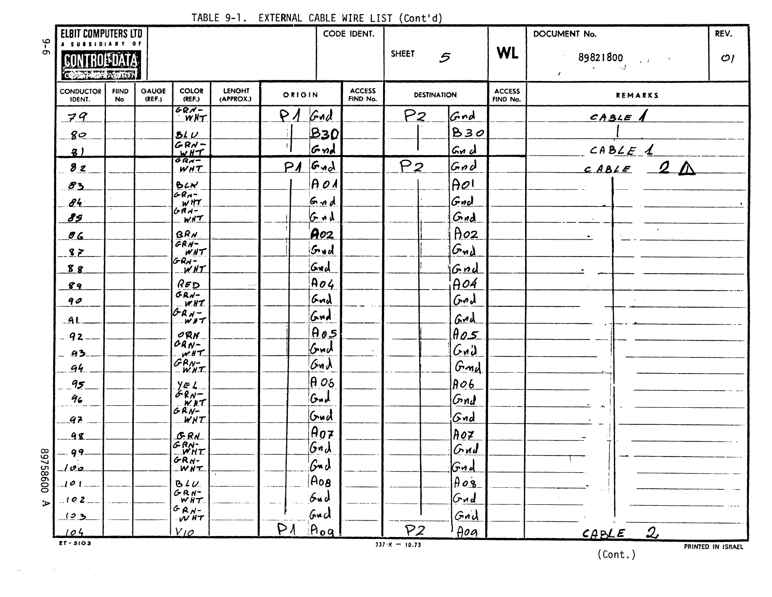
TABLE
9-1.
EXTERNAL
CABLE
WIRE
LIST
(Cont'd)
ELBll
COMPUTERS
LTD
'fl.
SUBSIDIARY
Of
0'\
CONDUCTOR I
FUND
GAUGE COLOR LENGHT
IDENT.
No
(REF.)
(REF.)
(APPROX.)
ORIGIN
CODE
IDENT.
ACCESS
FIND No.
SHEET
5
DESTINATION,
WL
ACCESS
FIND
No.
DOCUMENT No.
89821800
.!
REMARKS
REV.
01
_._"1_~
__
r-
__
.~_'UJ,i
____
__
~J_~~.J
__
_____
.
___
e.z
__
.c;..,.,J
_
______
eitaLE
,
.-.!~---------~:~-.---
~~fr--
--1-'
--~~1----
CA&~/LJ
______
..
__
~_~
__
._-t
___
16
;;;i_
.
~~
__
jt€-~e!.
____
__
2_::?
____
~"J
_____
. c
~_F
a.
&.
p~~~_~
_______
..
__
.
_.IA.t?A
___
.
___
. _
_____
.1}C21_+
____
..
___
_
~fl,.,-
!
--~"--.
--'
-----
.wlfT
__
---
--J:<;'~J
"-
~.--
G"'J_1 I «
1--
,
(?fff'l-.
'
_U__
_w/I-r
.-
----t--,-:"A-
-------·t--:-~~tl-
--_.
.---
-1---
__
~_'__
__
.
~~I'!-,-_
,AfL2_
Lil~_q~
______
,
____
_
(J.~tI-
I : I
~
__
~_L-_
---
(j-tt'
._--
___
Ir
__
;?-"tt
___
._
'--'-'H~-~Jl-I
I
t--
------
r.~
.
__
WK
ti--".J-
_____
I
}G~
----t------
y,
l]~D
11!!l_~
__
.---.
-I~-I
I
:t
__
't~_
_ _
~'::H-r
. .
l6-",~
____
. . .
~~Lt_--t___---
_i\L
__
--.
--
~1t:N-=r
--
~
._1G.14~_~
----
.
~-cl--t=r-----.
-
qz,--
-r---
~W--"
..
_--
. .
1:~J
.--.
I
:R0:a-
-~~---
__
.
___
.~H~
r-------
-.--
..
_-
..
--.--~
G.
__
.
__
.
__
_
-.,q~-
~~l~r
:~~j.-..
-----f----
~~-I----I--
__
--'-
_._q~
_____
...
___
.~EI.
..
_
IftPo
..
---Rc2L
1
--.l-
1
----
~,
tf.~N-
!&~J
(1...,J
. --
--
~
ft.*('
. -
-T6.--~f
.
Gd-
I
----.,
_._f'J-'"
.-
--
_____
J,r'JlT_
~
-
...
--.
..
__
"'=-+1--+1
____
_
CX>---~.i.-
~R,!-
!~~J
---. ,Ii{l!rl--l----"
~
-'
q,'1-
~~.r
--
-f-
J'
"
~---
..
--
------r-
~
_lffl...:L-
._WIIT.._
-:----
..
____
.
__
;r;...
--
..
---
...
--
'--;{r'~-IIt-----tI----
~
._l-D 1
..
_________
t;
L
£L
____
..
_____
._
lAos
_ _
__
.
__
.
~
o.~_
.
_____
1-
____
_
o
&RN-G
J
>
..
I()Z
__
_____
1----_
WHt'.
____
._.
.-. -
..
-
".
------
.....
___
--(r~-Lf
_.
___
_
-~~-~-
...
-
---
;:~~·~·_:::l'X;~·~
--
~2--
~;l--I
CI)Pi..E
~
I-
I
--I~-
-r
:
r~
--------
.-
---
..
-
----
----------_.
--
I!T-
.5103
337'H -10.73 (Cont.)
PRINTED
IN
ISRAEL
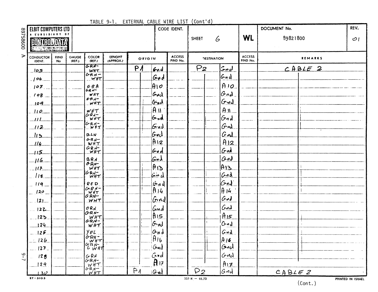
ex>
I.D
.......
(J1
ex>
0'1
a
a
:P-
\.0
I
o"J
InUl-L-
:.I-I.
L...I\II-I\llrlL_
VnUL-L...
UJ.I\L-
L..J..,JI
VVII""
_
HBIT
COMPUTERS
LTD
CODE
!'DENT.
A
S'
U 8
SID
I A R Y D f
~,.'UI[U~~J
SHEET
G
..,.
~>
..
--.
....
~ ""lr.
r~
...
·r;~·:-
,
•..
' .(.
··.'J'tjY~;.I:.(:jJ~
CONDUCTOR :
FUND
I,
GAUGE
.
eOtOR
' tl!NGI'iT
O'R'I'GI'N'
ACCeSS "lESTINATION
IDENT. ;
No
(REF.)
:
(REF.)'
(APPROX.)' FIND No.
.-'-()~
6-ll.tI-
PA
~d._
P2
G-",j _
---
.---.
..
WH~
----
-.--.-
Crttl'l-
(;~J
Go"e!
./Ok.
__
.
-------
--_.-.
_.lItJJ-r
.-----
--
-_._-
---._---.---
J
O'l.
__
I
t:-«A
c--.JA1O
A/G._
...
------ G-R,..J-
----
..
-
.----
---_._---
-_.-
--
------.
(
(j!8--
i WHT.
__
IG.)4J.
GflJ _
.----
-_._--_.
--.--
..
--
--
-----
-
, 60ft
tI-
I
I~
J
G-.X1.J._
_.LO~
,
_wHL
----~-
-'-
....L-....i
---..
..
_----
----
,
iAJL'
.AJ1_
.ILQ._.
--
1-.
__
..
.
wilL.
-------
.--
Cr~.l-
I-._Gt.'f\~
I
_Ll.L-
. w
tI-r,
1-----_
..
-'-"--
____
•...
_0-
----_
..
'--
1,-,-
:G.,J
..
._U2:_
CrR-tl-
I
I~
J
,G>1cL_
-----
.W
(1.1':
)1. ....
------
! J
_..11?l..-.
(:!,Lf,I
-------
t---.'G.~.
-------
G~L
.-1L't--
!
6-RrJ-
A\2
A.J2....
.wl'ii
.-~
...
-.
6-2,J-
~
IrrnA
-1-15--
._.~H1:
_116,._
,
_____
.S
Rl''-_f-
____
V;~!
---
.
t~:
6-RN-
e-~
~-
~\~
._
Ul--.-
I
...
•
'V'I
HI
'.
--
r;.
'A,J- ' i Q",a
....
II S.
_____
.
___
!
wH"r
____
---
r'-
.~.cl
----
---f.-----
.--
! ' , I
/('1.
_
'_'_
._
..
_r;~
D.
I 6-
J'
___
1._
'_y'l~
._-
'--.--
...
~-
(
2."
,{)1
f?
rI-
'
...
__
! _f\
14
R
/4
'
_..
_____
.
___
'to!
liT'
.
_____
uRN-
.
---
-.-
---
-_
....
. /21-_
__
.____.W
tlT.
____
.--
~--r&!\~
(J.t*J
.
__
.-
-
------
r
2l.--
.__
()
RtJ.
..
~~
CTRN-
.-
--1c.,.J
.
__
..
__
12~
..
_.
____
.
WH,
~
fit~
..
---
! tf!J5-
tTRri-
-.J.~L
__
WIf,",(
_____
...
_.
;--1
0
."J
I
o->1J
.
__
._-
-_
.
-.
...
/Z;._
f----
...
__
. Y
fit..
___
~_"Io.
~
J
--.
._
..
~_
C
...
.!l._
6-RtI-
'
__
._
_.~
~
1(' ..
__
~--.
(}J'._._
_.'../'],12
_
__
.
___
wH-r
_____
--------
(;r
n tJ- .
...
_.!
G.ItJ
---1-.
e."cA
._
..
/27-
_ .
___
..
G
WH1
.
__
..
_
----_.
I
'Z
~
&-
R,J
_
._
......
_.
611d
-------
____
.
&~A.
CrR-tV-
A
It
_.1
~!t
~v
H'T
..
____
_____
.fhL.
CrR,rl-
'-P'A-;G~J
--.
I
1,c)
WUT
\=>2
G.,,'"
ET-SIO;J
33H(
-
10.73
DOCUMENT
No.
REV.
WL
89821800
c9/
ACCESS
REMARKS
FIND No.
---
c.
aSL€'
2
-.
_.---_
..
.
_._-----_.------_.
..
----,--
I
I
------
-.
I
-------
..
---
i I
---
I
._1-,--.
I
---
..
I
..
_-
-_._-----_.
.
-----.
.---
..
1==-----
"-_.
--.-.--
---.
------
C.A-BL~
2
PRINTED
IN
ISRAEL
(Cont.
)
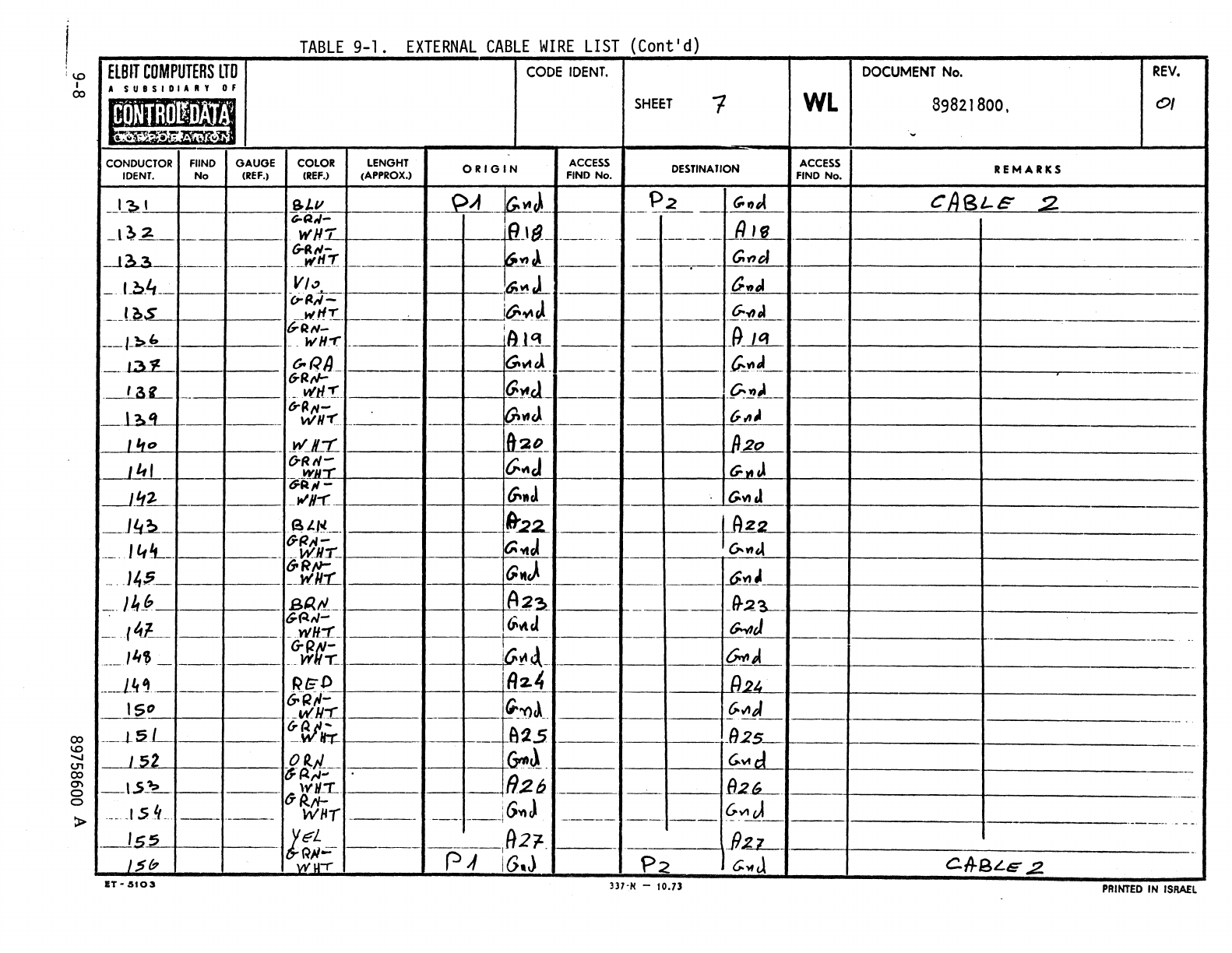
'\0
I
00
00
\0
.......
U'I
00
~
o
o
>
TABLE
9-1.
EXTERNAL
CABLE
WIRE
LIST
(Contld)
HBJT
COMPUTERS
LTD
CODE
IDENT.
A
SUBSIDIARY
Of
Jimn
HI
I
tlf1!'f!
SHEET
1
."':'~~M~v'J}
CONDUCTOR
FUND
GAUGE
COLOR LENGHT
ORIGIN
ACCESS DESTINATION
IDE
NT.
No
(REF.)
(REF.)
(APPROX.) FIND
No.
_-'-~
I
aI-v
___
QA
_~!!~
__
r-----
P2
~.,~
(;.QII-
_.
..--.-~.--
I .il.-lL
_l~~
__
---
--
.WWi"
I.
__
~IS-
--------.-
_.lA3_
G-R1i-'"
__
.
..!'tl._
~!'L
---_._-
..
_'ff
______
-------
-.
·-----r--
_Lb_Lt_
VI"
1~~rL
-~~
crP,;---
--
____
t~s
__
tiff!
__
r------.
iu-¥\J
._--
_~-,{}L
_
__
--.--..1
___
...
__
6-Rf'I-
_
ia_l~
__
_(tl!L
---l-~~-
___
WH
.
..,.
--
__
-,31
t;.RIJ
_
G~_~_
--.-
---
_
_~YI~_
{TRill-
__
'3L
---
__
Vid_!'
_
G~_cl_
---
--
_~:!J~
__
__
alL
6-~,,-
~~~--
6{1~
--
WHT'._
-----.
--
--
-----
1-
".,,,
_
.Yf..L-r...
r---
--
~~-
~.
---1~1
vRtI-
G
..
J
G-IIIJ
__
_
yyiJ.-r
--1_~"
6AII-
Gt.J
(;.Yld
t;'/L~
_.J~
_~l"L_
ft.22..
---_
..
~2-
___
I
L,~
__
vFlA-
(;;.,.J
.
V.
III,",
_
___
W.HJ'..
1------
----.14$-
6oRftI-
G
..
J.
y_Y!)_
.w'1tL
1--------
._--
__
Ikf,
BP.t!.._
A~~
_ -
.---
_9-.'2.'L
___
{4J
__
G(.tl'l-
6~J
tMlJ
__WH~
__
--
1----
_~~dT.._
----
-
fo---i--,-
____
lit,
_
-----
-$t1J.--
--
--
y."L
_____
1.11,
___
f---
ru;-D
fhz.4
--
.i2L-
-~!'
($,-Qfj;'"
~~cA
__
(;.",,J
__
vl.N~
-
~-{!I'~
...
_-
__
-1sL
--
A25
JJ2S_.
__
1.22
3M
..
&-t_!l
_
G.~d
__
826
_I.s-~
(J1l}"T.-
-
--
82-'-
___
-'
5.~_
---
------
WI4,
----
:G~J
._0
___
-
---
._-
~_V1d
---,
__
'ss
le-L
_____
,1)
2'1-_
-P2..L-
_
---
-.
. QII';::-
PA
16.J
1St?
WM""T"
P2
G:~J
IIT-aI03
337-11
-10.73
DOCUMENT
No.
REV.
WL
89821800.
c?/
~
ACCESS
REMARKS
FIND
No.
cABLE"
2-
-.
.--.
...
-
--
---
I
----.
1-----
--.
-_.
--
--
---
--
---
.
--
...
0_.
-
._-_.-.
-
--.
--
C/l-SLE
.2.
PRINTED
IN
ISRAEL
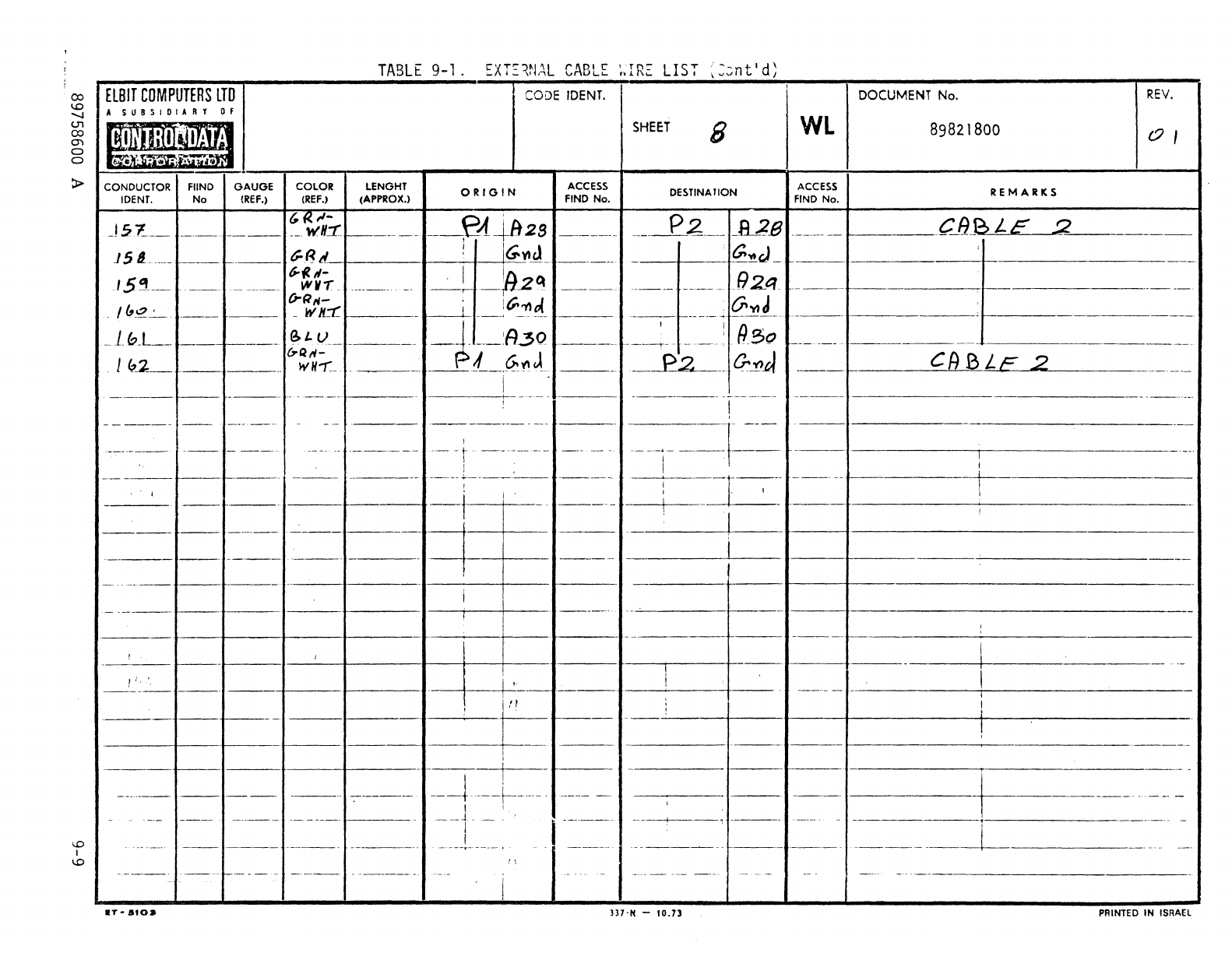
00
1.0
'-I
tTl
00
0'>
o
o
ElBIT
COMPUTERS
LTD
A
SU8SIDIARY
Of
TABLE
9-1.
EXE~N,4.L
CABLE
~,IR'::
LIST
;:~nt'd)
CODE
IDENT.
SHEET
B
DOCUMENT
No.
REV.
WL
89821800
01
~
I
CONDucrOR
I
FUND
GAUGE
COLOR LENGHT
IDE
NT.
No
(REF.)
(REF.)
(APPROX.)
ORIGIN
ACCESS
FIND No. DESTINAIION
ACCESS
FIND
No.
REMARKS
<.D
I
\.0
J57..
___________
:~;'f-'---------
--_eA-+A2B
______
.
___
--.2.2
___
-R2EI------L--
(28-'6
LE
~=----
151
_________
_
~_
~~d
!
ic;."J
_
~___
~~"LI_--I-~---I_-------
I 54i---
________
6-~,;.
_______
_
__-
~
__
~2q
____
_ _________
F12&r
_ I
(,_~.:.._
_
____
~~i-z:
____
i
___
:60_~~_
___
_
____
.
__
._
~_
0'1'11_
1
___
1
------'1_
_______
_
-
Lb.L___
_ - __
e.L
u_
-----
-t
-.-~f13Q
.
______
~---
i
R_80
_ ll?_Z______
__
I?!~;,
_
__
-
______
L_:{?",J
__
-.ez-
__
G-:!?4
I
____
~
CA
B
LE
2
--
I
--
1--
----1-----
---I----
---------
----
----
!
-----1
---.--------
----1----.------
---1----·-
---l-
i
----
'-----:....-1----
,
-=~=---=:=--=~~=----I
-~
-.-t--r-I-
--r--=-l--
-~t
---
1
T
I
--J---
-t-
+---1---+-
!
,.
------
......
--1
I, 1 t I
J----J-----I
I -
-----
-----'-----+---
-----~--+__-I
I
[:=1----
-------
.
---.--
---
--
-
----1-------
-/-------
-.
------
I
I
I
I 1
---t---~----
-
, '
I
-T-
I
T
------1---1----1
-------
--~-,1:=1-=-~1-----
t------
1---1-----1
-------=L -
_T-
al03
);]-1(
-
10.73
PRINTED
IN
ISRAEL
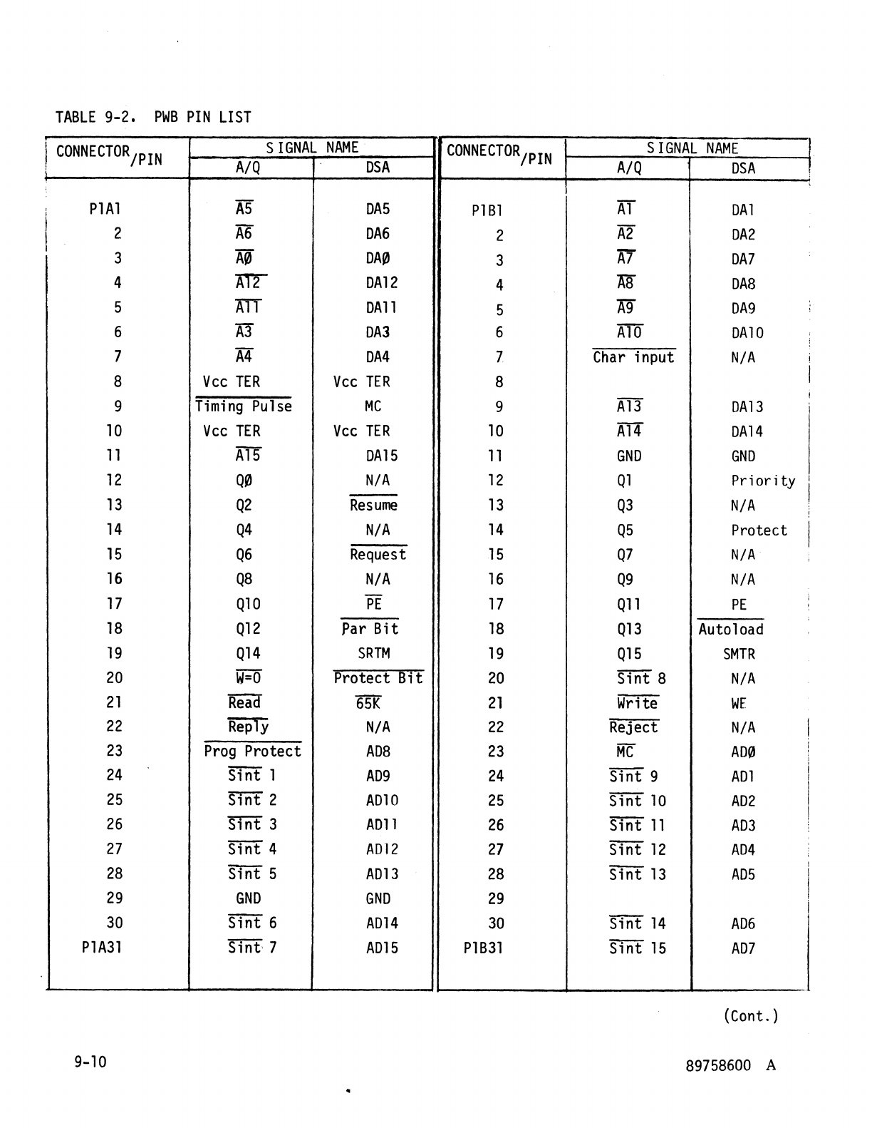
TABLE
9-2.
PWB
PIN
LIST
I
CONNECTOR/PIN
SIGNAL
NAME
CONNECTOR/PIN
SIGNAL
NAME
I
A/Q
DSA
A/Q
DSA
,
\
I
P1Al
AS
DA5
Pl
Bl
AT
DAl
2
A6
DA6
2
A2
DA2
3
A0
DA0
3
Ar
DA7
4
AT2
DA12
4
AS
DA8
5
All
DAll
5
A9
DA9
1
6
A3
DA3
6
A10
DA10
7
A4
DA4
7
Char
input
N/A
i
8
Vee
TER
Vee
TER
8 I
I
9
Timing
Pulse
MC
9
Al3
DAl3
10
Vee
TER
Vee
TER
10
A14
DA14
11
A15
DA15
11
GND
GND
12
Q0
N/A
12
Ql
Priority
13
Q2
Resume
13
Q3
N/A
14
Q4
N/A
14
Q5
Protect I
15
Q6
Request
15
Q7
N/A
16
Q8
N/A
16
Q9
N/A
-,
17
Q10
PE
17
Q11
PE
,
18
Q12
par
Bi
t
18
Q13
Autoload
19
Q14
SRTM
19
Q15
SMTR
20
w=O
Protect Bit
20
Sint 8
N/A
21
Read
65K
21
Write
WE
22
Rep1y
N/A
22
Reject
N/A
23
Prog
Protect
AD8
23
MC
AD0
24
Sint 1
AD9
24
Sint 9
ADl
25
Sint 2
AD10
25
Sint
10
AD2
26
Sint 3
ADll
26
Sint
11
AD3
27
Sint 4
ADI2
27
Sint
12
AD4
:
Sint 5 S i
nt
13
I
28
ADl3
28
AD5
I
29
GND
GND
29
I
i
30
Sint 6
AD14
30
Sint
14
AD6
P1A31
Sint 7
AD15
P1B31
Sint
15
AD7
(Cont.)
9-10
89758600
A
•
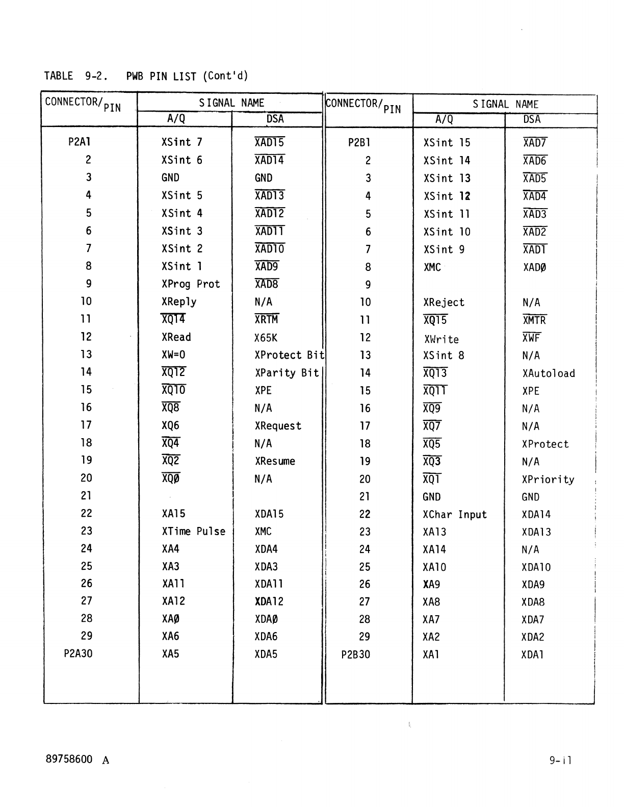
TABLE
9-2.
PWB
PIN
LIST
(Cont'd)
CONNECTOR/PIN
SIGNAL
NAME
CONNECTOR/PIN
SIGNAL
NAME
I
A/Q
DSA
A/Q
DSA
P2A1
XSint
7
XAD15
P2B1
XSint
15
XAD7
2
XSint
6
XAD14
2
XSint
14
XAD6
i
!
3
GND
GND
3
XSint
13
XAD5
4
XSint
5
XAD13
4
XSint
12
XAD4
I
5
XSint
4
XAD12
5
XSint
11
XAD3
I
I
6
XSint
3
XAD11
6
XSint
10
XAD2
7
XSint
2
XAD10
7
XSint
9
XAD1
I
I
8
XSint
1
XAD9
8
XMC
XADflJ
9
XProg
Prot
XAD8
9 i
I
10
XRep1y
N/A
10
XReject
N/A
I
11
XQT4
XRTM
11
XQ15
XMTR
I
I
12
XRead
X65K
12
XI,Jri
te
XWF
I
i
13
XW=O
XProtect Bit
13
XSint
8
N/A
I
I
14
XQ12
XParity Bit
14
XQ13
XAutoload
!
I
XQ10
WiT
t
15
XPE
15
XPE
I
i
16
XQ8
N/A
16
XQ9
N/A
I
I
I
17
XQ6
I
XRequest
17
XQ7
N/A
I
18
XQ4
I
N/A
18
XQ5
XProtect I
I I
19
XQ2
i
XResume
19
XQ3
N/A
I
20
XQflJ
I
N/A
20
XQ1
XPriori ty I
21
I
21
GND GND
I
22
XA15
XDA15
22
XChar
Input
XDA14
I
I
23
XTime
Pu1
se
XMC
23
XA13
XDA13
I
,
24
XM
XDM
24
XA14
N/A
25
XA3
XDA3
25
XA10
XDA10
!
!
26
XA11
XDA11
26
XA9
XDA9
i
I
27
XA12
XDA12
27
XA8
XDA8
I
28
XAflJ
XDA0
28
XA7
XDA7
29
XA6
XDA6
29
XA2
XDA2
I
I
I
P2A30
XA5
XDA5
P2B30
XA1
XDA1
I
I
I
89758600
A
9-il

r.:ll
~I
c.!)'
S:
<I
~I
01
,
I
I
I
1
I
I
I
I
I
I
I
I
I
I
I
1
I
I
I
I
I
1
I
I
COMMENT SHEET
MANUAL
TrrLE
TTL
A/Q-DSA Bus
Expander
Hardware
Reference/Customer
Engineering
Manual
PUBLICATION
NO.
___
8_9_75_8_6_0_0
_______
REVISION
__
A
___________
_
FROM NAME:
____________________________________________________
~
________
__
BUSINE~S
ADDRESS:
_____________________________________________________________
__
COMMENTS:
This
form
is
not intended to
be
used
as
an
order
blank. Your evaluation of
this
manual will be welcomed
by
Control
Data
Corporation. Any
errors,
suggested
additions
or
deletions,
or
general
comments
may
be
made below.
Please
include page
number.
STAPLE
STAPLE
FOLD
-----------------------------------~
BUSINESS
REPLY
MAIL
NO
POSTAGE
STAMP
NECESSARY
IF
MAiLED
!N
U.S.A.
POSTAGE
WILL..
BE
PAID
BY
CONTROL
DATA
CORPORATION
PUBLICATIONS
AND
GRAPHICS
DIVISION
4455
EASTGATE
MALL
LA
JOLLA,
CALIFORNIA 92037
FiRST
CLASS
PERf~IT
NO.
3,3
LA
JOLLA.
CA.
I
I
I
I
I
::..l
Iz
.....
l...."l
I~
IS
I~
I~
1°
I
I
I
I
I
---------------------
---------------~
FOLD
STAPLE
STAPLE
I
I
I
I
I
I
I
I
I
I
I
I
I
I
I
,1
