A 5958 4362 9_Series_300_Display_Color_Card_Theory_of_Operation_Oct85 9 Series 300 Display Color Card Theory Of Operation Oct85
User Manual: A-5958-4362-9_Series_300_Display_Color_Card_Theory_of_Operation_Oct85
Open the PDF directly: View PDF  .
.
Page Count: 12
II!
*
IHHbd
'#b&bbtHMW**Jd
"!
I "
HEWLETT-PACKARD
co.
NOTE:
!'his
page
provides
a
running
histery
ef
changes
fer
a
mUlti-page
drawing
which
cannot
conveniently
be
re-issued
cempletely
after
each
change.
When
making a
change,
list
fer
each
page
all
before-
and-after
numbers
(within
reasen;
use
judgement,and
use
"extensive"
revisien
nete
if
less
ef
past
histery
is
tolerable,
or
retype
cemplete
page)
and
asseciate
with
each
a symbel
made
up
ef
the
change
letter
and a
serial
subscript
to
appear
here
and on
the
page
involved
(there
enclesed
in
a
circle,
triangle,
er
other
attentien-getting
outline).
Ltr
REVISIONS
DATE INITIALS
A
As
Issued
(0
-,
'1
1
.-,
\
Title
Theory
of
Oper
a
tio
n
Description
Oete
By
Brad
Reak
Sheet
No.
1
of
1'-
Or~wing
~,o.
A-5958-43f)?-9
9320-3246
(6/15)
4EELQLa:a:&a'dl&!&lJOJKWJiS
t.._d. Lo]\"!f'Tit'!ff
,.f
..
"F4f'
4#AFl
z;;;
i~M,.Il+tH!'
t
r.
HEWLETT
~
PA.CKARD
CO.
I
SERIES
300
DISPLAY
COLOR
CARD
(
The6ry
of
operation
FINAL
B.t:'ad
Reak
Hewlett
Packard
Company
Fort
Collins
Systems
Division
See
Pg.
1
for
Rev~.
lDWgN~A-5958-4362.9
IPAGE
:2
of
l?,
DESCRIPTION
Theory
of
OP
9320-5037
EZL&l1Il1&it&&a;
...
=m:g;Q!J1\JGJf~LiJifu&iifuff,f.4;)
,lfwFff¥;,
,!fQl¥h.,
4H?U#,
i.lMM
, # ;
44_P4&
._
I
I
I
I.
, htH
"ItH'#:WL
bllrirl+"
4Thy
±tHe
'/0"' , H
HEWLETT
-
PACKARD
CO.
I
Scope
I
C;!ap
t'er
~.
-t-------------------.----.--
I
____
---'
______ _
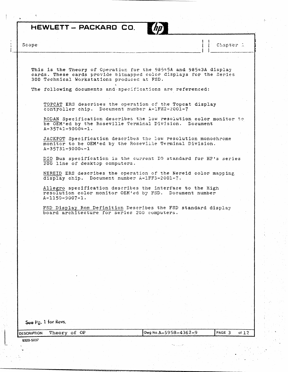
This
is
the
Theory
of
Cperatior:
for
the
98545A
and
98543A
displaJ'
cards.
These
cards
provide
bitmapped
color
displays
for
the
Series
300
Technical
Workstations
produced
at
FSD.
The
following
documents
and·
specifications
are
ref~renced:
TopcAT
ERS
descriDes
the
operation
of
the
Topcat
display
controller
chip.
Document
nu~ber
A-lFH2-2001-7
RODAN
Specification
describe~
the
low
resolution
color
monitor
to
be
OEM'ed
by
the
Roseville
Terminal
Divjsion.
D~cument
A-35741-90004-l.
JACKPOT
Specirication
describes
the
low
resolution
mohochrome
monitor
to
be
OEM'ed
by
the
Roseville
Terminal
Division.
A-35731-90004-1
DIO
Bus
specification
is
the
cu~rent
10
standard
for
HP's
series
200
line
of
deskt0p
computers.
NEREID ERS
desc~ibes
the
operation
of
the
Nereid
color
mapping
display
chip.
Document
number
h-1FF3-2001-7.
Allegro
specification
describes
the
interface
to
the
High
resolution
color
monitor
OEM'ed
by
FSD.
Document
number
A-1150-9007-1.
FSP
Display
Rom
Definition
Describes
the
FSD
standard
display
board
architectur€
for
series
200
computers.
See Pg. 1
for
Revs,
DESCRIPTION
Theory
of
OP
Dwg
No.A-5958-4362-:-,9
PAGE 3
of
I?
9320·5037
WIIdlWiiiiZCUlk!t!iJlXlii;;
..
m:aUi{I;;;Jt4iffiiAiim2MGiiiJ·"".4,
I %
¥E¥,
.;;;;;'4
"m
¥q
74
A."".
_
4PW¢.444t4t
,'.'.
au;
;'&'
•.
Rh',4
;#i..n4i"';;;._';WJf.$4'I~t»f;;
..
~"~"
I
HEWLETT
--
PACKARD
CO.
--------_._-------------------_._-------
GENERAL
DESCRIPTION
ChaptEl'
2
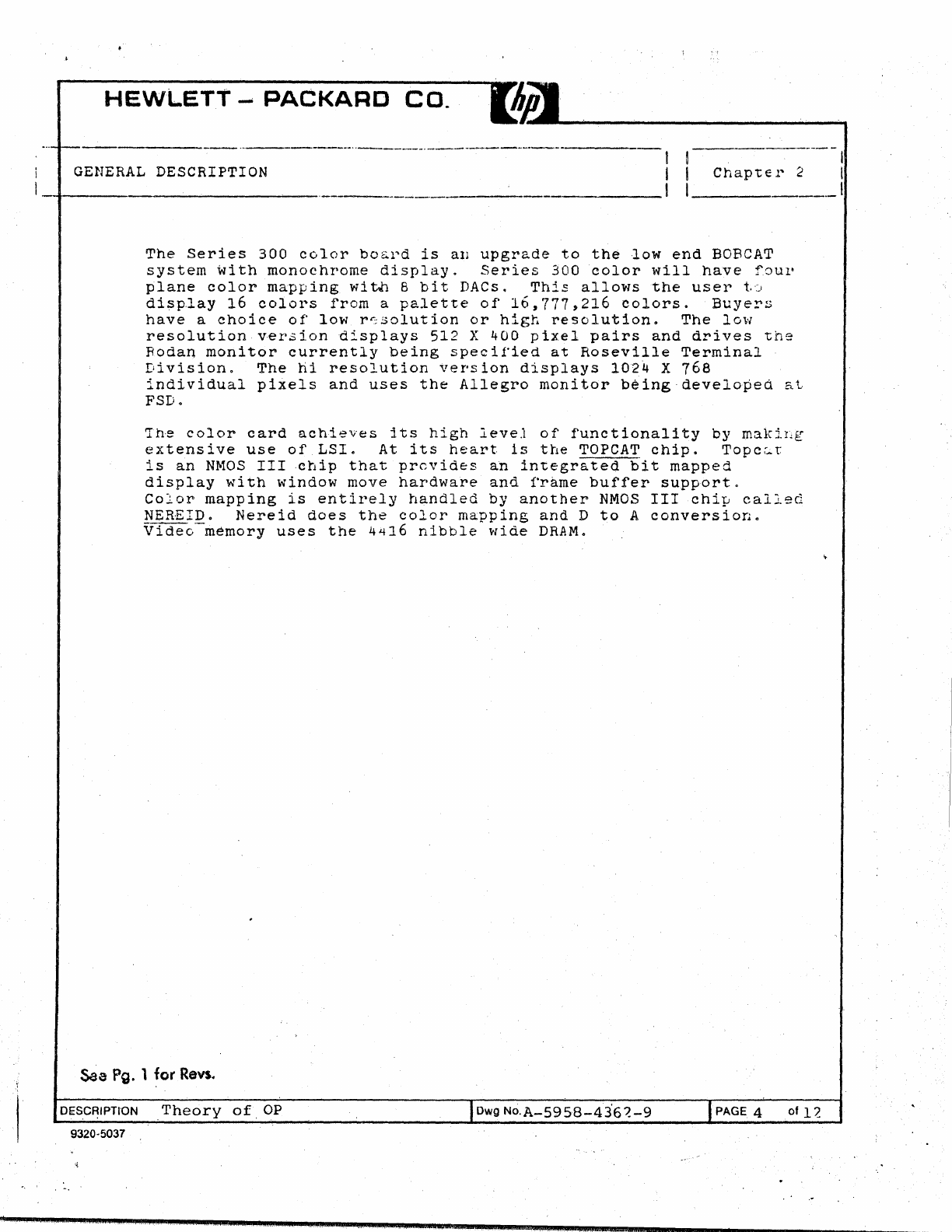
The
Series
300
color
bo&r-d
is
all
upgrade
to
the
low
end
BOBCAT
system
~ith
monochrome
display.
Series
300
color
will
have
four
plane
color
mapping
wi
t.h
8
bit
DACs.
This
allows
the
user
t..::.,
display
16
colors
from
a
palette
of
16,777,216
colors.
Buyers
have
a
choice
of
low
r~301ution
or
high
resolution.
The
low
resolution
version
displays
512
X
400
pixel
pairs
and
drives
the
Rodan
monitor
currently
being
specified
at
Roseville
Terminal
Division.
The
hi
resolution
version
displays
l02~
X 768
individual
pixels
and
uses
the
Allegro
monitor
b$ingdevelo~ed
at
FSD.
Th~
color
card
achieves
its
high
level
of
functionality
by
makil~g
extensive
use
of
LSI.
At
its
heart
is
the
TOPCAT
chip.
Topc~t
is
an
N:t-10S
III
.ctdp
that
provides
an
integra.
ted
bi
t
mapped
display
with
window
move
hardware
and
frkme
buffer
support.
Color
mapping
is
entirely
handled
by
another
NMOS
III
chip
called
NEREID.
Nereid
does
the
color
mapping
and
D
to
A
conversion.
V-ideo-memory
uses
the
4'-i16
nibble
wide
DRAM.
Sea
Pg.
1
~or
Revs.
DESCRIPTION .
Theory
of
OP
PAGE 4
of
l~
9320-5037
¥4
A 4144; A
i$U4L
#2AW#4
4.
.. 24
44
g
44
4.$
4
44
.4;)MA.
iabL.rI
+ L*#t:!lt!.W
hrlttwirwlL
8"blet!*W·"·rII'·"tk
.
.,....,
~
...
HEWLETT
-
PACKARD
CO.
-------_._------
-_._-_.
__
._---------------------------------
FUNCTIONAL
DESCRIPTION
I
Cl1~ptel'
3
1
____
.-
3.1
Topcats
and
Video
R~rn
The
Topcat
is
the
h~art
of
the
display
board.
Topcat
can
best
be
descri~ed
as
a
Frame
Buffer
memory
manager
and
window
ttover.
It
takes
memor.y
date:.
in
the
on
board
frame
buffer
and
Cl-'ea"Ces
pixel
data.
This
0peration
is
essentially
invisible
to
the
rest
0f
th0
~ysteffi.
To
the
system)
the
i'r·ame
buffer
memory
appe-~rs
a
nc,r'r:lal
system
ram
but
organized
in
a
format
that
makes
graprlics
manipulation
easier.
The
c~lor boa~d
uses
the
TMS
4416
nibb:e
wide
DRAM
as
described
in
tile
TOPCAT
ERS.
Both
high
and
low
resolution
boards
have
1',}-JI
planes
of
memory.
The
low
res
board
uses
eight
memo~y
chips
~~~
plane
(U
01
to
U
08).
Hi
resolution
uses
16
m~mory
chips
~~r
plane
(U-01
to
U-16).
Series
damping
resistors
R
01
to
R d4
and
RP
01,
damp
the
RAM
address,
RAS
and
CAS
lines.
R-05
TO
F.-Q7
i:ee~.
th;
Topcat
DIP
port
inactive
during
normal
board
~peratio~
bUT
'
allow
a
3065
board
tester
to
use
the
DIP
port·
for
trouble!hoOTin.
TOPCATS.
Topcat
organizes
the
l'ramebuffer
into
an
array
fixed
to
1024
pixels
across
and
either
512,1024
or
2048
lines.
It
is
possible
to
select
the
number
01'
displayed
lines
via
programm.able
Topca
t
registers.
The
98543A
card
displays
1024
individual
pixels
across
and
40D
lines
down.
This
leaves
112
lines
of
undisp:ay~d
frame
buffer
available
for'
temporary'
storage
of
graphics
information.
Since
single
horizontal
pixels
would
far
exceed
th
bandwidth
0 f
mos
t
low
cos
t
r.1.Oni
tors,
it
is
so
ftwares
'
responsibility
to
always
use
double
pixels.
The
effect
is
to
give
horizontal
resolution
better
than
512
pixels
without
exceeding
monitor
bandwidth
specs.
Single
pixel
snifting
is
allowed
but
there
must
always
be
at
least
2
pixels
between
adjacent
horizontal
dots.
The
98545A
uses
a
much
higher
performance
mon'itor
and
therefcre
does
not
require
software
to
use
double
pixel
algorithms.
3.2
Nereia
Color
Map
The
color
board
has
four
plane
colormapping.
Mapping
is
entirel
under
control
of
the
NEREID
chip.
See
the
Nereid
ERS
for
particulars
on
its
operation.
Since
only
four
pl,anes
are
used
and
Nereid
supports
eight,
the
top
four
planes
remain
unused
and
Sea
Pg.
1 for
Rell&.
DESCRIPTION
Theory
of
OP
Dwg
No,A-5958-4362-9
PAGE 5
of
1
~
9320·5037
---
:zza:uaUiiianwa:::n;t;tt::ma.ltlWMtti;d&O.iJ..ii.,i
..
r I ;
,\.,
I¢.
.44#@i!E§4ij
MW
•.
4U/i$&2i4&t&U&W.a
mLM41K4F
,'4"q
..
Hi$-
Q *$ii1I1,-"'''-
1,£11;
. q
HEWLETT
~
'PACKA~O
COe
Due
to
peculiarities
in
the
N0reid
colormap,
it
is
pos~~~:e
~o
d
a
write
read
cycle
to
Ner'eid
to
fast.
This
is
esps-I-:~l.)
..
.i
..
:':'::t!'t'''t
with
a
combinaticn
or
fast
processor
and
low
resol~~l~n
(j5~12Y
card~
The
pi."'irr
..
c.Y'y
l"eason
for
this
is
that
the
c:l-:.:(.'l'.
J.S
not
f::ls"t
enough
to
clec.i.I' l';e:::'t;ids
bl~SY
bit
i:::efoI'e
another
:0:L"'J
cycle
(;;:":1
start.
The
error
1s
seen
as
a
bus
error
t~m~out
at
the
CPU.
Th~
fix
is
to
use
a
NOP
or
ot~.er
delay
technique
to
prevent
cC·!l==~~'..~tive
Nereid
access
cycl~s.
Nereid
needs
at
least
16
dot
clock
cycles
~etween
accesses.
In
the
case
of
the
low
~esolution
displ~y
~35.904MHz
clock)
this
is
445ns
before
starting
another
Nereid.
access.
In
the
future,
raster
p:::'c1ccssors may
make
tr.is
shew
':lp
on
even
the
Hi
resolution
card.
It
is
advisable
to
always
che~k
the
16
cycle
rule
as
stated
3.be;vE'
\·:heu
'\'lriting
code
1'02"'
Ne-reia..
Nereid
uses
older
NMOS
techliOlogy
so
therefore
re;L~i!"'f.!s
r.,:):-,".;
-
...
l"~a
.SV
and
-2V.
U4
is
a
voltage
regulator
that
suppl~e~
Nerei~
wit
6.5V
at
Vclk
and
Aclk.
Aclk
js
isolated
from
Vclk
t·y
trte
lOKpas
:filter
1.1
and
C28.
This
keeps
noise
generated
by
·\"~.il':
fl'C'Ii:
coupling
directly
to
~he
ou~puts
via
an
internal
Nereid
~a~h.
1/4
of
U2,
QIC
and
Q8
compose
2
3.75V
regulato~
tc
su,ply
Nereid
VI
supply.
1/4
of
U2
with
Ol~
and
reference
voltag~
so~r~e
~1
suppiy
the
-2V
needs
of'
N~r'eid
::.nd
the
res
to
tbe
t;02.l'·j,
Nereid
requires
a
con.s-:ant
~·:i.:"'I'.=:nt
.source
to
establist
a
reference
f'or
the
DAC'
s.
'l'Lts"2.,:,
2.~,:,:omplished
using
or
a!1:p
V')
and
the
resistor
netw·ork
co;..p:-;~:.~.j~).~'
.~·-{I~,
R6,
Rl1,
R12,
Hl.:~
,:'\.l
~~
R14.
The
nominal
value
is
·~~t;
mi(':.I·':I.::4A:~p;;)
into Irei'
v;j
1;:n
::L\'
~,_
'.f!
node
or
R4
and
R6.
3.3
Logic
Interface
to
CPU
The
internal
section
of
the
~isplay
card
is
isolated
a~d
b~ffere
from
the
CPU
bus
via
Ul0,
U15,
U21,
u26
and'U32.
The
Data
buffers
UI0
and
U15
always
point
from
the
CPU
to
the
displ~y
cal"
\
unless
there
is
a
read
request
to
the
board
from
the
processor.
Decoding
is
accomplished
by
the
6ustom
PAL
U19
and
decoder
u36.
u36
with
U31
and
U38
create
a
progranunable
register
3
in
the
middle
of
the
display
ROM
address
space.
A
write
of
any
value
t
register,l
forces
the
card
to
reset
its
interrupts
by
clearing
U38.
V37
Returns
0
for
unused
planes
during
a
read
from
the
frame
buffer.
Supposedly,
this
makes
software
easier
to
implement.
Topcats
used
together
are
very
sensitive
to
anythi,ng
that
may
cau~e
the~
to
become
urisynchronized.
This
could
happen
by
doing
See Pg. 1
for
ReV$.
DESCRIPTION
Theory
0 f
OP
DwgN~A-5958-4l62-9
PAGE
6
of
1
~
9320·5037
M ..
4th
Mil;
$1M_Mi.
d."
rrn
qki4QN"94A~·1
_cw
4
LA$
# •
$==&
Ra;:w.X;XMw.r,ea &J¥"W!t\."',.AZWCQ!!Riijidm
..
@,,:.
~"l.!If.iIlMfiffi
m
_iil,.,WMLi!M&1iJ"UQl,JJOOUUM£,OO
£
.•
U$
..
0.44.'44
Q
HEWLETT-
PACKAR'O
,COo
a
chi
p S
f'
lee
t
at
a
t.i
m €'
\-\T
hen
:i
n d i v i d l,.Ut 1
~
r..r:::-
pc
at
s
mayo
r
!iI
:i
Y
!;
C t
see
the
select
:::ignal.
Ie's
being'rhat
they
are"
soine
m:!;';fli;
:::t:':e
the
select
and
some
might
not.
'.:-;:;15
\'lo'u,ld
cause
considerc:~b.l€;
video
diztortion.
US
cor!'ects
tr::i~
problem
by
synchronizing
NCS,
NSUDS
and
NSLDS
to
Topcats
clock.
Topcats
and
Nereids
generate
their
own
DTACK
and
this
is
f~d
to
the
CPU
bus
thr~
U14
and
U9.
Requ~sts
to
read
ROM
U20
or
wri~~
to
register
1
01"
registe'r
3
are
DTACKed
by
walking
a 1
tbru
sl"~ift
register
U1S.
~he
9S5~5A
and
9854JA
boards
will
generally
confo~m
~o
DIO
specifications~
with
the
following
exceptions.
(
1.
Shape
factor
will
be
Series
300.
2.
Interrupts
allo~
all
7
levels
to
be
programmed
V"
':l
r'egis
ter
3.
3.
Edge
connector
is
Series
300
CPU
pinout
not
standard
DIO.
4.
IMA
is
generated
but
not
brought
to
the
connectdr
(See
U9
pin
S)
•
• 4
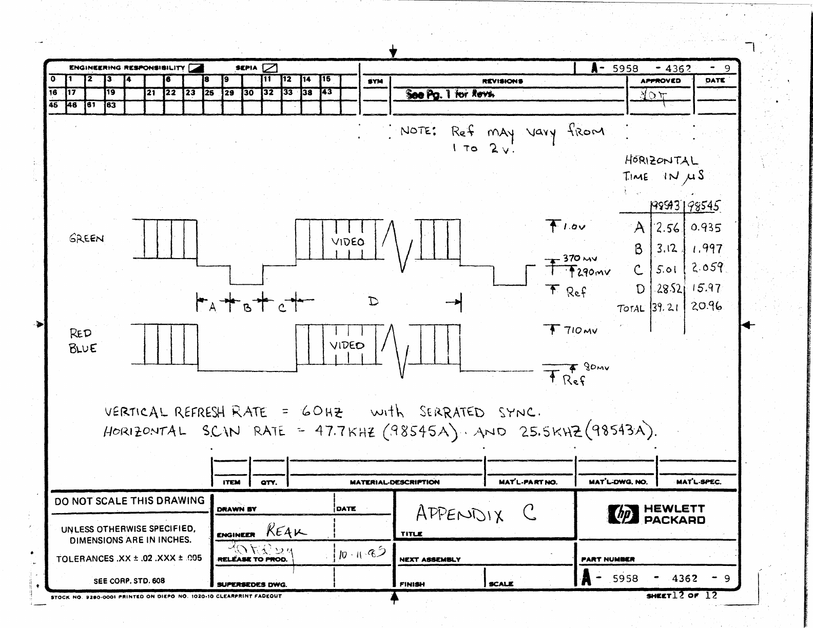
Video
Amplifies
and
Output
Typical
video
levels
seen
at
the
BNe
connectors
are
shown
in
appendix
C.
It
is
important
to
reme~ber
that
the
video
sig~al
rides
on
a
1.5
volt
DC
level.
The
video
level
is
adjusted
by
pot
R6
which
c~ntrols
the
current
source
~ha~
supplies
Nereids
Iref
pin.
For
the
purposes
of
this
explanation,
the
green
amplifier
will
be
explained
because
the
red
and
blue
are
similar
but
withQut
the
sync.
The
transistor
Q6
with
resistor
Rsb
and
R24
form
a
current
to
voltage'
converter
that
converts
the
current
sink
of
Nereids
output
to
a
voltage
that
varies
fr6~
9.7
volts
to
9.0
volts
nominal
at
the
base
of
Q3.
The
video
drive
stage
is
a
simple
emi
tter
follol'ler
that
drives
the
moni
tor
through
zener
CR3
'and
the
common
mode
chock
T2.
T2
serves
to
prevent
a conunon
mode
signal
from
escaping
to
the
outside
world
and
causitig
RFI
problems.
Zener
CR3
drops
a
constant
6.8
volts
to
bring
the
nominal
level
no
signal
level
to
about
1
volt~
Since
most
monito~s
use
composite
sync
on
green,
it
is
necessary
to
mix
the
0.3
volt
sync
signal
with
the
video.
This
is
accomplished
with
the
resistor
R38
acting
to
suck
out
enough
current
to
lower
the
voltage
a
the
base
of
Q3
by
0.3
volts
during
,horizontal
or
vertical
sync
as
controlled
by
the
XOR
gate
corinect~d
to
Ul1.
Zener
CR9
biases
the
t~ansistors
Q5, Q6, Q7,
and~9
into
~iJ'~
P
w
. 1 for
ReV).
DESCRIPTION
Theory
of
OP
Owg
No.A-5958-:-4362-9
PAGE 7
of
12
9320·5037
WQ2
4&
q'MifJttiJlhS.tkC
,DMMit
AUA
....
i¥
..
AitWt$
4
ad.
MJL
";,
(
44
q.M .. @
##4=
...
'
"41
.ta,
&t.Jd,.,AMM4i4=.JMMJM
QUMM#iiHMfWI9I1Il¥HM/iiiWi"M@
i!HI.p&\'blHth1ti
! h
HEWLETT
--
PACKAR'O
CO.
condue
tion
and
c:.ll~)\";::
th.::'
,::Xl""".'~'nt
to
V
('I
1
tage
actj.cn
of
the
circuit.
Zener
CR2
bia.;;;es
(:2,
Q3
c:..r:<l
Q4
and
preV~n·ts
p,~'weI'
supply
noise
from
getting
jnt~
the
video.
Any
moriitor
used
with
the
color
cards
sho~ld
be
AC
coupled
due
to
the
1.5
volt
bias
imposed
on
the
video
sjgnai.
See
appendix
C
for
exact
details
of
~he
video
level
abd
timitig.
3.5
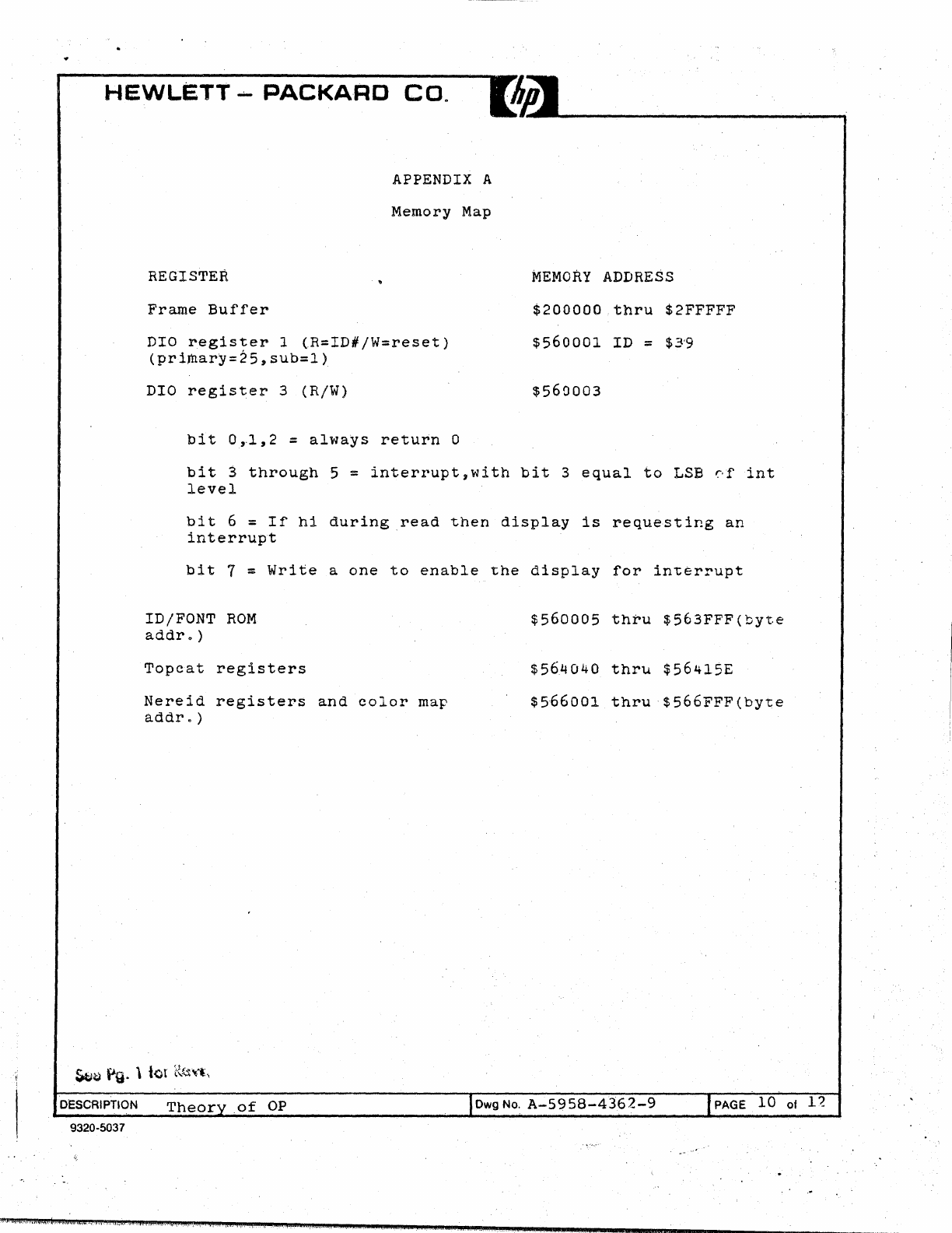
Memory, Map
M~mory
configuration
conforIns
to
the
FSD
Display
ID
!,-OM
Definition.
The
color
boards
implementation
is
sho~n
i~
appendix
A.
Tl'le
Frame
buffer
and
the
Topcat
register
set
are
fix(f(:.
in
internal
address
space.
The
98545A
Topcat
registers
ove~iay
the
Topc~ton
the
68010
processor
board.
De$election
of
the
Topcat
cn
trie
processor
board
is
ac~omplished
by
a
.switch
located
on
"Cf!!::
processor
board.
,
3.6
Interrupt
Structure
The
interrupt
structure
is
similar
to
DIO
with
the
except.ion
of
being
software
progranunable
to
all
7
levels.
Sof'tiHl.re
must
set
the
ihterrupt
level
and
turn
on
interrupts
by
writing
to_IE
~s
per
DTO.
Interrupts
s.re
extended
DIG
by
using
D3
tr~!'o;J.~n
D5
~t
register
$560003.
Some
consistency
is
obtained
witI'.
D:-O'oy
continuing
to
use
posit!ve
logic
and
by
making
D3
as
the
LSB.
a
receiving
an
inte~ru~t
and
ve~~fying
the
interrupt
is
co~~~g
fro
the
color
card,
the
processor
must
then
poll
the
Topca~
chips
to
determine
the
interrup~ing
device.
3.7
Clocks
and
Timing
The
system
clock
controls
the
entire
timing
of
the
display
card.
It
is
based
on
EeL
technology
to
allow
the
system
to
run
at
a
high
enough
clock
rate
to
a~ive
a
Hi
resolution
monitor.
The
main
o$cillator
is
bas~d
on
TTL
levels
and
is
converted
tc
a
EeL
level
by
U35.
The
actual
description
of
the
circuit
would
be
long
winded
and
probably
useless
to
the
reader.
Instead,
you
ar,
encouraged
to
study
the
timing
diagrams
with
the
clock
schem&~ic
close
by.
The
only
peculiar
part
of
the
c1rcui~
would
be
the
adjustable
duty
cycle
of
Dclk2.
This
is
accomplished
by
using
adjust,able
RC
networlc
composed
of
R85,
R79
and
c16.
The
capacitor
is
allowed
to
charge
to
a
level
high
enough
to
trigge
U27
and
is
then
forced
to
discharge
when'Qll
is
turning
on
the
the
state
change
uf
U27.
Qll
is
made
stable
by
the
temperature
compensation
circuit
labeled
cbias.
Cbias
room
temperature
voltage
level
should
be
about
-2VDC.
U27
is
forced
to
oscillat
f'"
.
:-.;.
l.'
;,"
, I
'/'
J
joc
"Vv~"
'OESC'RIPTION
Theory
of
OP
9320-5037 PAGE 8
of
12
OOl£J4itiamimaiJi&!lilllYiGGi;;;;lilAars;1dB,iGh;&JiimriSkl"J3JQt"i!l!ill11IDM;L..,,"\
R
kiii"AfS,i
,
.1#
,C\fI1-,
¥,
p
..
=
k.
.44$
4i
*"
.'it
UA
',$'$Ii.'
...
HEWLETT
--
PACKARD
CO.
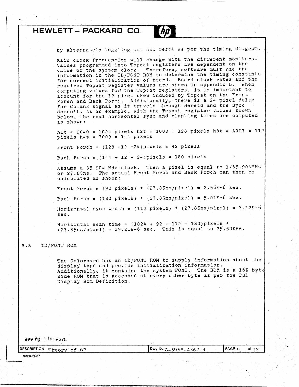
by
alterna~ely
toggling
set
end
resu~
~~
per
the
timing
di&gr~m.
Main
clock
frequencies
will
change
with
the
different
monit0rs.
Values
programmed
into
Topcat
l'egisters
are
dependent
on
the
value
of
the
system
clock.
Therefore,
software
must
use
the
information
in
the
ID/FONT
ROM
to
determine
the
timing
cons~ants
for
correct
initialization
of
board.
Bo~rd
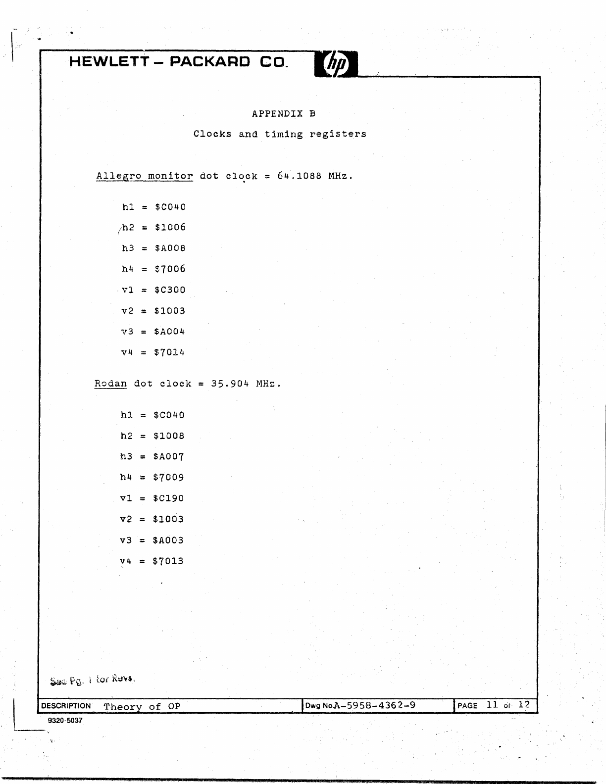
clock
rates
and
the
required
Topcat
register
values
are
shown
in
appendix
B.
When
computing
values
fo~
The
Topcat
registers)
it
is
important
to
account
ror
the
12
pixel
skew
induced
by
Topcat
on
the
Front
Porch
and
Back
Porc~..
Addi
'tional.iy,·
thel'e
is
a
24
pixel
delay
for
Cblank
signal
as
it
travels
through
Nereid
and
the
Sync
doesn't.
As
an
example,
with
the
Topcat
register
~al~es
shown
~elow,
the
real
horizontal
sync
and
blanking
times
are
computed
as
shown:
hIt
=
C040
=
1024
pixels
h2t
=
1008
;
128
pixels
h3t
=
A007
=
112
pixels
h4t
=
7009
=
144
pixels
Front
Porch
=
(128
-12
-24)pixels
=
92
pixels
Back
Porch
=.(144
+
12
+ 24
)pixels
=
180
pixels
Assume
a
35.904
MHz
~10ck.
Then
a
pixel
is
equal
to
1/35.904MH~
or
27.85ns~
Th~
actual
Front
Porch
and
Back
Porch
can
then
be
calculated
as
shown:
Front
Porch
=
(92
pixels)
*
(27.85ns/pixel)
=
2.56E-6
sec.
Back
Porch
=
(180
pixel~)
*
(27.85ns/pixel)
=
5.0lE-6
s~c.
Horizontal
sync
width
=
(112
pixels)
*
(27.85ns/pixel)
=
3.12E-6
sec.
Horizontal
scan
time
=
(1024
+
92
+
112
+
180)pixels
*
(27.85ns/pixel)
=
39.21E-6
sec.
This
is
equal
to
25.50KHz.
3.8
ID/FONT
ROM
The
Colorcard
has
an
ID/FONT
ROM
to
supply
infor-mation
about
the
dis~lay
typ~
and
provide
initia1ization
information.
Additionally~
it
contains
the
system
FONT.
The
ROM
is
a
16K
byte
wide
ROM
that
is
accessed
at
every
other
byte
as
per
the
FSD
Display
Rom
Definition.
DESCRIPTION
rrheor
of
OP
DwgN~A-59~8-4362-9
9320·5037
of,, R.
,HF,T
...
,
£'4,;
#H4.1{ -. .
&44
4.A#
44
$.
OUi·
HEWLETT
--
PACKARO
COm
APPENDIX A
Memory
Map
REGISTER
Frame
Buffer
DIC
register
1
(R=IDNjW=reset)
(primary=25,sub=1)
D10
register
3 (R/W)
bit
Or1,2
=
always
return
0
MEMORY
ADDRESS
$200000
thru
$2FFFFF
$560001
ID
= $3'9
$560003
bit
3
through
5 =
interrupt,with
bit
3
equal
to
LSB
0f
int
level
bit
6 =
If
hi
during
read
then
display
is
requesting
an
interrupt
bit
7 =
Write
a
one
to
enable
~he
display
for
in~errupt
ID/FONT
ROM
$560005
thru
$
563FFF
(byt.e
addr
0 )
Topcat
registers
$564040
thru
$564l5E
Nereid
registers
and
color
map
$566001
thru
$566FFF(byte
addr.
)
O'ESCRIPTION
Theor
.of
OP
Dwg No.
A-5958-4362-9
PAGE
10
of
l~
9320-5037
iii]\,Jii,
t
;,
",
",W%(.
L;;'n
kit(
r
i,i¥ff4ifIifiRA
r ,
..
ilFfHM4¥M.f;
If#R
,4
4,,4
f{44Y4
.
"g
-
4.
#W
L¢
........
,
,e;
#.xuae.¥ $
.(44
•.
4,.;U%rn.AA#4
,.-
H'E'WLETT
-
PACK,ARC
co.
APPENDIX
B
Clocks
and
timing
registers
Allegro
monitor
dot
clock
:;
64.1088
MHz.
~
h1
:;
$C040
(h2
:;
$1006
h3
=
$A008
h4
=
$7006
vI
:;
$C300
v2
=
$1003
v3
=
$A004
v4
:;
$7014
RQdan
dot
clock
:;
35.904
riJHz.
hl
=
$C040
h2
:;
$1008
h3
=
$A007
h4
:;
$7009
vI
=
$C190
v2
=
$1003
v3
=
$A003
v4
=
$7013
DESCRIPTION
Theory
'of
oP
DwgNoA-5958-4362-9
PAGE
11
Of
12
9320-5037
A¥#
424A4
#44:;:>
44
4.
Z$@44
$44
42
$.
42MEE..
4#_44
44.
$
4=_
$
ilMM5
.AQt7iilAiDianu
4#_
¥i4i
4_.;
$$\$44$#214 . #
Uk
...
;;r
+
-1
ENGIN.EERtNG
·RESPONSI.IL.I~
~
.SEPIAIZl
A-
5958
-
436~
- 9
0 1 2 3 4 8 8 9
11
12 14 . 15 .
."IM
fItrIlSfONS
I
Aa.IIIOVEO
PATE
16
. 11
19
21
22
23
32
33
43
-
..
e;
..
1 lor
Itm.
'~()1
25
29
30
38
45
~6
81
63
-
-
NaTf.:
RQ.·~
MA~
\Ja;'f~
~ROM
\
10
'2.
V .
!-toR,
~ON
TAL
tIME
IN.?S
;
~~S43-
195'4£:
·1
I I
~
T/.ov
A
'2.5"'
,
O.Q35
bKtEN
VIDEO
I t I B
3.t2
; I,QQ7
n~~
l I ' "
Z-~OMV
c:
S.ot
'2..051
!
~A+~+C.+
~
T
Re.t
D
2.'6.52'
15/17
D TOTAL
3~.
2..1
~o·9"
.
.,
III
I
[II±+~
If\;
.~
REP
I
T710,.""
B\.Ut
'"
<tDMV
T\Z~~
VERi\c.A L
R.Ef"RfSt-\
R/~TE
::
c,OH~
w\i"- StRRA1El)
s'YNc..
·
l-IoRt
rONI
A L
~.('\N
RAlt.
--
47.7KHl
CQ8S45A)"
/'\NO
t.s. 5
K\\~
(9~
S4?'·~\).
1 .
.-
1-:-1
M"TERIAL-IXSCRtP'TION
I
MAT'L.PARTNO.
I
MAT·'-'DWQ.
NO.
I MATOL·SP£C.
DO
NOT
SCALE
THIS
DRAWING
I
DRAwNlIY
I
DATE
AVPE~l:J
\ '"
c:
(h~
HEWLETT
I
~'
,'lPACKARD
UNLESS
OTHERWISE SPECIFIED,
f<E4.~
I
,
ENGINEER
•
TITLE
DIMENSIONS ARE
IN
INCHES. . I
j,!~)
r\'
i
~
~)
1.\
' r I
In.;;
TOLERANCES
.XX
± .02
.XXX
± ,005 .R£L.tAR
TO
PROD.
) ',/0'
II'
6
,NEXT_V
Ir~N_
I
SCALE
·A
-
5958
see
CORP. STD.
608
-
4362
- 9
SU
.....
D£SDWG.
I
FINISH
•
~
-..
~
-
